WO2013172018A1 - Dispositif électronique - Google Patents
Dispositif électronique Download PDFInfo
- Publication number
- WO2013172018A1 WO2013172018A1 PCT/JP2013/003070 JP2013003070W WO2013172018A1 WO 2013172018 A1 WO2013172018 A1 WO 2013172018A1 JP 2013003070 W JP2013003070 W JP 2013003070W WO 2013172018 A1 WO2013172018 A1 WO 2013172018A1
- Authority
- WO
- WIPO (PCT)
- Prior art keywords
- panel
- piezoelectric element
- electronic device
- display unit
- housing
- Prior art date
Links
- 239000000463 material Substances 0.000 claims abstract description 71
- 239000002184 metal Substances 0.000 claims description 39
- 239000000853 adhesive Substances 0.000 claims description 10
- 230000001070 adhesive effect Effects 0.000 claims description 9
- 238000010438 heat treatment Methods 0.000 claims description 5
- 241000746998 Tragus Species 0.000 claims description 4
- 230000007423 decrease Effects 0.000 abstract description 3
- 230000003014 reinforcing effect Effects 0.000 description 12
- 238000005452 bending Methods 0.000 description 7
- 238000010586 diagram Methods 0.000 description 7
- 238000000034 method Methods 0.000 description 6
- 125000002066 L-histidyl group Chemical group [H]N1C([H])=NC(C([H])([H])[C@](C(=O)[*])([H])N([H])[H])=C1[H] 0.000 description 5
- 210000000988 bone and bone Anatomy 0.000 description 5
- 210000005069 ears Anatomy 0.000 description 5
- NIXOWILDQLNWCW-UHFFFAOYSA-N acrylic acid group Chemical group C(C=C)(=O)O NIXOWILDQLNWCW-UHFFFAOYSA-N 0.000 description 4
- 210000000845 cartilage Anatomy 0.000 description 4
- 238000004891 communication Methods 0.000 description 4
- 210000000883 ear external Anatomy 0.000 description 4
- 229920005989 resin Polymers 0.000 description 4
- 239000011347 resin Substances 0.000 description 4
- 230000002238 attenuated effect Effects 0.000 description 3
- 230000008602 contraction Effects 0.000 description 3
- 230000006870 function Effects 0.000 description 3
- 239000011521 glass Substances 0.000 description 3
- 210000000860 cochlear nerve Anatomy 0.000 description 2
- 238000001514 detection method Methods 0.000 description 2
- 210000000613 ear canal Anatomy 0.000 description 2
- 230000005764 inhibitory process Effects 0.000 description 2
- HFGPZNIAWCZYJU-UHFFFAOYSA-N lead zirconate titanate Chemical compound [O-2].[O-2].[O-2].[O-2].[O-2].[Ti+4].[Zr+4].[Pb+2] HFGPZNIAWCZYJU-UHFFFAOYSA-N 0.000 description 2
- 229910052451 lead zirconate titanate Inorganic materials 0.000 description 2
- 239000007788 liquid Substances 0.000 description 2
- 238000012986 modification Methods 0.000 description 2
- 230000004048 modification Effects 0.000 description 2
- 230000005236 sound signal Effects 0.000 description 2
- 229920000544 Gore-Tex Polymers 0.000 description 1
- 210000003423 ankle Anatomy 0.000 description 1
- 230000005540 biological transmission Effects 0.000 description 1
- 239000000919 ceramic Substances 0.000 description 1
- 239000000470 constituent Substances 0.000 description 1
- 230000008878 coupling Effects 0.000 description 1
- 238000010168 coupling process Methods 0.000 description 1
- 238000005859 coupling reaction Methods 0.000 description 1
- 210000000624 ear auricle Anatomy 0.000 description 1
- 230000000694 effects Effects 0.000 description 1
- 230000005674 electromagnetic induction Effects 0.000 description 1
- 239000012530 fluid Substances 0.000 description 1
- 239000006261 foam material Substances 0.000 description 1
- 239000003365 glass fiber Substances 0.000 description 1
- 239000004973 liquid crystal related substance Substances 0.000 description 1
- 230000003287 optical effect Effects 0.000 description 1
- 230000002093 peripheral effect Effects 0.000 description 1
- 229920006327 polystyrene foam Polymers 0.000 description 1
- 239000010453 quartz Substances 0.000 description 1
- VYPSYNLAJGMNEJ-UHFFFAOYSA-N silicon dioxide Inorganic materials O=[Si]=O VYPSYNLAJGMNEJ-UHFFFAOYSA-N 0.000 description 1
- 230000035882 stress Effects 0.000 description 1
- 238000010897 surface acoustic wave method Methods 0.000 description 1
- 229920003002 synthetic resin Polymers 0.000 description 1
- 239000000057 synthetic resin Substances 0.000 description 1
- 230000008646 thermal stress Effects 0.000 description 1
- 229920001187 thermosetting polymer Polymers 0.000 description 1
- 210000003454 tympanic membrane Anatomy 0.000 description 1
Images


Classifications
-
- H—ELECTRICITY
- H04—ELECTRIC COMMUNICATION TECHNIQUE
- H04R—LOUDSPEAKERS, MICROPHONES, GRAMOPHONE PICK-UPS OR LIKE ACOUSTIC ELECTROMECHANICAL TRANSDUCERS; DEAF-AID SETS; PUBLIC ADDRESS SYSTEMS
- H04R17/00—Piezoelectric transducers; Electrostrictive transducers
-
- H—ELECTRICITY
- H04—ELECTRIC COMMUNICATION TECHNIQUE
- H04M—TELEPHONIC COMMUNICATION
- H04M1/00—Substation equipment, e.g. for use by subscribers
- H04M1/02—Constructional features of telephone sets
- H04M1/03—Constructional features of telephone transmitters or receivers, e.g. telephone hand-sets
- H04M1/035—Improving the acoustic characteristics by means of constructional features of the housing, e.g. ribs, walls, resonating chambers or cavities
-
- H—ELECTRICITY
- H04—ELECTRIC COMMUNICATION TECHNIQUE
- H04R—LOUDSPEAKERS, MICROPHONES, GRAMOPHONE PICK-UPS OR LIKE ACOUSTIC ELECTROMECHANICAL TRANSDUCERS; DEAF-AID SETS; PUBLIC ADDRESS SYSTEMS
- H04R2460/00—Details of hearing devices, i.e. of ear- or headphones covered by H04R1/10 or H04R5/033 but not provided for in any of their subgroups, or of hearing aids covered by H04R25/00 but not provided for in any of its subgroups
- H04R2460/13—Hearing devices using bone conduction transducers
-
- H—ELECTRICITY
- H04—ELECTRIC COMMUNICATION TECHNIQUE
- H04R—LOUDSPEAKERS, MICROPHONES, GRAMOPHONE PICK-UPS OR LIKE ACOUSTIC ELECTROMECHANICAL TRANSDUCERS; DEAF-AID SETS; PUBLIC ADDRESS SYSTEMS
- H04R2499/00—Aspects covered by H04R or H04S not otherwise provided for in their subgroups
- H04R2499/10—General applications
- H04R2499/11—Transducers incorporated or for use in hand-held devices, e.g. mobile phones, PDA's, camera's
-
- H—ELECTRICITY
- H04—ELECTRIC COMMUNICATION TECHNIQUE
- H04R—LOUDSPEAKERS, MICROPHONES, GRAMOPHONE PICK-UPS OR LIKE ACOUSTIC ELECTROMECHANICAL TRANSDUCERS; DEAF-AID SETS; PUBLIC ADDRESS SYSTEMS
- H04R2499/00—Aspects covered by H04R or H04S not otherwise provided for in their subgroups
- H04R2499/10—General applications
- H04R2499/15—Transducers incorporated in visual displaying devices, e.g. televisions, computer displays, laptops
-
- H—ELECTRICITY
- H04—ELECTRIC COMMUNICATION TECHNIQUE
- H04R—LOUDSPEAKERS, MICROPHONES, GRAMOPHONE PICK-UPS OR LIKE ACOUSTIC ELECTROMECHANICAL TRANSDUCERS; DEAF-AID SETS; PUBLIC ADDRESS SYSTEMS
- H04R7/00—Diaphragms for electromechanical transducers; Cones
- H04R7/02—Diaphragms for electromechanical transducers; Cones characterised by the construction
- H04R7/04—Plane diaphragms
- H04R7/045—Plane diaphragms using the distributed mode principle, i.e. whereby the acoustic radiation is emanated from uniformly distributed free bending wave vibration induced in a stiff panel and not from pistonic motion
Definitions
- the present invention relates to an electronic device that vibrates a panel by applying a predetermined electrical signal (audio signal) to a piezoelectric element, and transmits the vibration of the panel to a human body to transmit air conduction sound and bone conduction sound to a user.
- a predetermined electrical signal audio signal
- Patent Document 1 describes an electronic device such as a mobile phone terminal that transmits air conduction sound and bone conduction sound to a user.
- air conduction sound is sound transmitted to the auditory nerve of a user by vibration of air that is caused by vibration of an object being transmitted to the eardrum through the external auditory canal.
- Patent Document 1 describes that bone conduction sound is sound transmitted to the user's auditory nerve through a part of the user's body (for example, cartilage of the outer ear) that contacts the vibrating object. ing.
- Patent Document 1 In the telephone set described in Patent Document 1, it is described that a short plate-like vibrating body made of a piezoelectric bimorph and a flexible material is attached to the outer surface of a housing via an elastic member. Further, in Patent Document 1, when a voltage is applied to the piezoelectric bimorph of the vibrating body, the piezoelectric material expands and contracts in the longitudinal direction, causing the vibrating body to bend and vibrate, and the user contacts the vibrating body with the auricle. It is described that air conduction sound and bone conduction sound are transmitted to the user.
- a vibrating body is attached to the outer surface of a housing such as a mobile phone terminal. For this reason, it is necessary to touch a small vibrating body protruding from the outer surface of the housing to the ear, and there are cases where the usability is poor. Therefore, by placing the vibrating body on the back surface (inner surface) of a panel such as a mobile phone terminal and deforming the panel due to deformation of the vibrating body, air conduction sound is generated with respect to the object (ear) that contacts the panel. It is assumed that the bone conduction sound is transmitted.
- An object of the present invention is to solve a problem in an electronic device that vibrates a panel and to provide a good electronic device.
- An electronic device includes a piezoelectric element, a panel that supports the piezoelectric element, and a casing that holds the panel, and the panel transmits vibrations by vibrating air conduction sound and a part of the human body.
- a cushioning material is disposed between the panel and the housing.
- Both the piezoelectric element and the buffer material may be arranged on one end side in one direction in a plan view of the panel.
- the buffer material may be thinned away from the piezoelectric element in the direction of the other end.
- the buffer material may be bonded to only one of the panel and the housing.
- the housing may include a sheet metal as an insert member.
- the piezoelectric element may have a rectangular shape in a plan view, and the buffer material may be disposed outside the end in the longitudinal direction of the piezoelectric element.
- the housing may be composed of a first housing portion and a second housing portion that is located inside the first housing portion and includes the sheet metal.
- the buffer material may be arranged in the other end direction in the one direction of the panel rather than the piezoelectric element.
- the display unit may be held on the panel, and the cushioning material may contact the display unit.
- the buffer material may be in a pressed state before the vibration of the piezoelectric element.
- the casing may have a rectangular shape in plan view, and the length of one of the two opposing sides may be equal to or longer than the length from the antitragus to the lower leg of the antiaural ring.
- the length of the opposite two sides of the casing may be equal to or greater than the length from the tragus to the anti-ankle.
- the piezoelectric element may be bonded and fixed to the casing by a bonding member.
- the joining member may be a non-heating type curable adhesive.
- the bonding member may be a double-sided tape.
- the panel may be joined to the casing by a joining member.
- the joining member for joining the panel to the housing may be a non-heating type curable adhesive.
- the bonding member for bonding the panel to the housing may be a double-sided tape.
- the panel may constitute a part or all of the display unit, the input unit, and the cover of the display unit.
- the fixed portion of the piezoelectric element in the panel may be located outside the overlapping area with the display unit in plan view of the panel.
- the display unit may be fixed to the panel from the inside of the housing.
- FIG. 1 is a diagram showing functional blocks of a main part of an electronic device 1 according to an embodiment of the present invention.
- the electronic device 1 is, for example, a mobile phone terminal, and includes a wireless communication unit 5, a panel 10, a display unit 20, a piezoelectric element 30, an input unit 40, and a control unit 50.
- the wireless communication unit 5 has a known configuration and is wirelessly connected to a communication network via a base station or the like.
- the panel 10 is a touch panel that detects contact, a cover panel that protects the display unit 20, or the like.
- the panel 10 is made of, for example, glass or a synthetic resin such as acrylic.
- the shape of the panel 10 may be a plate shape.
- the panel 10 may be a flat plate or a curved panel whose surface is smoothly inclined.
- a detection method of the touch panel any method such as a capacitance method, a resistance film method, a surface acoustic wave method (or an ultrasonic method), an infrared method, an electromagnetic induction method, and a load detection method can be used.
- the display unit 20 is a display device such as a liquid crystal display, an organic EL display, or an inorganic EL display.
- the display unit 20 is provided on the back side of the panel 10.
- the display unit 20 is disposed on the back surface of the panel 10 by a joining member (for example, an adhesive).
- the display unit 20 may be bonded to the panel 10 with a bonding member (for example, an adhesive), or is separated from the panel 10 and supported by the casing of the electronic device 1.
- the piezoelectric element 30 is an element that expands and contracts or bends (bends) according to the electromechanical coupling coefficient of the constituent material by applying an electric signal (voltage).
- the piezoelectric element 30 may be a unimorph, bimorph, or multilayer piezoelectric element.
- the stacked piezoelectric element includes a stacked unimorph element in which unimorphs are stacked (for example, 16 layers or 24 layers), or a stacked bimorph element in which bimorphs are stacked (for example, 16 layers or 24 layers are stacked).
- the laminated piezoelectric element is composed of a laminated structure of a plurality of dielectric layers made of, for example, PZT (lead zirconate titanate) and electrode layers arranged between the plurality of dielectric layers. Unimorphs expand and contract when an electrical signal (voltage) is applied, and bimorphs bend when an electrical signal (voltage) is applied.
- PZT lead zirconate titanate
- the piezoelectric element 30 is disposed on the back surface of the panel 10 (the surface on the inner side of the electronic device 1).
- the piezoelectric element 30 is attached to the panel 10 by a joining member (for example, double-sided tape).
- the piezoelectric element 30 may be attached to the panel 10 via an intermediate member (for example, a sheet metal).
- the piezoelectric element 30 is disposed on the back surface of the panel 10 and is separated from the surface on the inner side of the housing by a predetermined distance.
- the piezoelectric element 30 may be separated from the surface on the inner side of the housing by a predetermined distance even in a stretched or curved state. That is, the distance between the piezoelectric element 30 and the inner surface of the housing is preferably larger than the maximum deformation amount of the piezoelectric element 30.
- the input unit 40 receives an operation input from the user, and includes, for example, an operation button (operation key).
- an operation button operation key
- the panel 10 can also accept the operation input from a user by detecting the contact from a user.
- the control unit 50 is a processor that controls the electronic device 1.
- the control unit 50 applies a predetermined electrical signal (a voltage corresponding to an audio signal of a call partner's voice or a ringing melody or music including music, etc.) to the piezoelectric element 30.
- a predetermined electrical signal a voltage corresponding to an audio signal of a call partner's voice or a ringing melody or music including music, etc.
- the acoustic signal may be based on music data stored in an internal memory, or music data stored in an external server or the like may be reproduced via a network.
- the piezoelectric element 30 When an electrical signal is applied to the piezoelectric element 30, the piezoelectric element 30 expands or contracts in the longitudinal direction. At this time, the panel 10 to which the piezoelectric element 30 is attached is deformed in accordance with the expansion or contraction or bending of the piezoelectric element 30, and the panel 10 vibrates.
- the maximum voltage of the electric signal applied to the piezoelectric element 30 by the control unit 50 is higher than ⁇ 5 V, which is an applied voltage of a so-called panel speaker for the purpose of conducting sound by air conduction sound instead of vibration sound, for example. , ⁇ 15V.
- the panel 10 even when the user presses the panel 10 against his / her body with a force of 3N or more (5N to 10N force), for example, the panel 10 generates sufficient bending vibration, and the user's body Vibration sound can be generated through a part (eg, cartilage of the outer ear).
- a part eg, cartilage of the outer ear.
- how much applied voltage is used can be appropriately adjusted according to the fixing strength of the panel 10 to the casing or the support member or the performance of the piezoelectric element 30.
- the panel 10 is bent by expansion / contraction or bending of the piezoelectric element 30.
- the panel 10 is bent directly by the piezoelectric element 30.
- the panel 10 is directly bent by the piezoelectric element means that the panel is specified by the inertial force of the piezoelectric actuator configured by arranging the piezoelectric element in the casing as used in a conventional panel speaker. This is different from the phenomenon in which the panel is deformed by exciting the region.
- the panel 10 is directly bent by the piezoelectric element means that the expansion or contraction or bending (bending) of the piezoelectric element bends the panel directly via the bonding member or via the bonding member and the reinforcing member 100 described later. Means that.
- the panel 10 bends and vibrates not only in the attachment region where the piezoelectric element 30 is attached, but also in the region away from the attachment region.
- the panel 10 has a plurality of locations that vibrate in a direction intersecting the main surface of the panel 10 in the vibrating region, and the amplitude value of the vibration is increased from positive to negative with time in each of the plurality of locations. Or vice versa.
- the panel 10 vibrates in such a manner that a portion having a relatively large vibration amplitude and a portion having a relatively small vibration amplitude are distributed randomly or periodically throughout the panel 10 at first glance. That is, vibrations of a plurality of waves are detected over the entire panel 10.
- the control unit 50 does not attenuate the piezoelectric element 30 in order to prevent the above-described vibration of the panel 10 from being attenuated.
- the maximum voltage to be applied may be ⁇ 15V. Therefore, the user can hear the sound by bringing his / her ear into contact with a region away from the above-described region where the piezoelectric element 30 is attached, for example, the center of the panel 10.
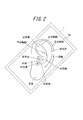
- the panel 10 may be approximately the same size as the user's ear.
- the panel 10 may be larger than the user's ear, as shown in FIG.
- the panel 10 corresponds to a length corresponding to the distance from the lower leg of the anti-annulus (lower anti-limb) and the distance from the tragus to the anti-annulus. A region wider than the region having a width to be oscillated may be vibrated.
- the panel 10 preferably has a length corresponding to the distance between a portion near the upper leg of the ankle ring (upper pair leg) in the ear ring and the earlobe, and a distance between the tragus and a portion near the ear ring in the ear ring. It suffices that a region having a width corresponding to is vibrated.
- the region having the above length and width may be a rectangular region, or may be an elliptical shape having the above length as the major axis and the above width as the minor axis.
- the average size of Japanese ears can be found by referring to the Japanese human body size database (1992-1994) created by the Human Life Engineering Research Center (HQL).
- the panel 10 is larger than the average size of Japanese ears, the panel 10 is considered to be large enough to cover the entire foreign ear.
- the panel 10 can cover the user's ears, and is tolerant of misalignment when applied to the ears.
- the electronic device 1 can transmit the air conduction sound and the vibration sound through a part of the user's body (for example, cartilage of the outer ear) to the user by the vibration of the panel 10. Therefore, when outputting a sound having a volume equivalent to that of a conventional dynamic receiver, the sound transmitted to the periphery of the electronic device 1 due to the vibration of the air due to the vibration of the panel 10 is less than that of the dynamic receiver. Therefore, it is suitable, for example, when listening to a recorded message on a train or the like.
- the electronic device 1 transmits vibration sound due to the vibration of the panel 10, even if the user wears an earphone or a headphone, for example, the user can touch the electronic device 1 to contact the earphone or the headphone. Sounds can be heard through headphones and body parts.
- the electronic device 1 transmits sound to the user by the vibration of the panel 10. Therefore, when the electronic device 1 does not include a separate dynamic receiver, it is not necessary to form an opening (sound outlet) for sound transmission in the housing, and the waterproof structure of the electronic device 1 can be simplified.
- the sound emission port is preferably closed by a member that allows gas to pass but not liquid.
- a member that allows gas to pass but not liquid is Gore-Tex (registered trademark).
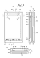
- FIG. 3 is a diagram schematically illustrating a main part of the mounting structure of the electronic device 1 according to the first embodiment.
- 3A is a front view
- FIG. 3B is a cross-sectional view taken along line bb in FIG. 3A
- FIG. 3C is a cross-sectional view taken along the line cc in FIG.
- the electronic device 1 shown in FIG. 3 is a smartphone in which a substantially rectangular (substantially rectangular) glass plate is arranged on the front surface of a housing 60 (for example, a metal or resin case) as the panel 10 in a plan view.
- a housing 60 for example, a metal or resin case
- the panel 10 constitutes, for example, a capacitive touch panel, and is supported (held) on the housing 60 via a joining member 70.
- the display unit 20 is bonded to the panel 10 via a bonding member 70 on the back surface excluding the upper portion on one end side in the longitudinal direction, which is one direction in plan view. That is, the display unit 20 is fixed to the panel 10 by the bonding member 70.
- the piezoelectric element 30 is bonded to the upper back surface on one end side in the longitudinal direction of the panel 10 via a bonding member 70 and supported by the panel 10. That is, as illustrated in FIG. 3A, the fixed portion of the piezoelectric element 30 is located outside the overlapping region between the panel 10 and the display unit 20 in plan view.
- the piezoelectric element 30 is fixed to the housing 60 via the panel 10 by the joining member 70.
- the piezoelectric element 30 has a substantially rectangular shape in plan view, and is bonded so that its long side is along the short side of the panel 10.
- the bonding member 70 is an adhesive having a thermosetting property or an ultraviolet curable property, a double-sided tape, or the like, and may be, for example, an optical elastic resin that is a colorless and transparent acrylic ultraviolet curable adhesive.
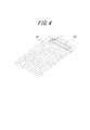
- FIG. 4 is a diagram illustrating an example of vibration of the panel 10 of the electronic device 1 according to the first embodiment.
- the display unit 20 is attached to the panel 10.
- the other end side of the panel 10 is less likely to vibrate compared to one end side of the panel 10 to which the piezoelectric element 30 is attached (hereinafter also referred to as a main vibration unit). Therefore, sound leakage due to vibration of the other end side of the panel 10 on the other end side of the panel 10 can be reduced.
- One end side of the panel 10 is directly bent by the piezoelectric element 30, and vibration is attenuated on the other end side as compared with the one end side.
- the panel 10 is bent by the piezoelectric element 30 so that the portion directly above the piezoelectric element 30 protrudes higher than the surrounding area in the long side direction of the piezoelectric element 30.
- the input unit 40 is supported by the housing 60 on the other end side in the longitudinal direction of the panel 10.
- a microphone mouthpiece 41 is formed in the input unit 40 as indicated by a broken line. That is, the piezoelectric element 30 is disposed at the upper part on one end side of the substantially rectangular casing 60, and the mouthpiece 41 is formed at the lower part on the other end side.
- the housing 60 includes a rear case (first housing portion) 62 and a front case (second housing portion) 61 located inside thereof.
- the rear case 62 is detachable from the front case 61.
- the front case 61 is configured to have a recess 63.
- the rear case 62 is configured to have a recess 64.
- the front case 61 and the rear case 62 are not limited to a concave shape, and can be configured in an appropriate shape.
- the front case 61 is configured to include a sheet metal 80 that is an insert member.
- the panel 10, the display unit 20, the piezoelectric element 30, and the input unit 40 are disposed in the recess 63 of the front case 61.
- a cushioning material 90 is disposed between the display unit 20 and the sheet metal 80.
- the buffer material 90 reduces the interference of the display unit 20 that bends and vibrates with the vibration of the piezoelectric element 30 with (contacts with) the sheet metal 80. That is, the cushioning material 90 is disposed between the panel 10 and the front case 61 which is a part of the housing, and interference between the panel 10 and the front case 61 is reduced.
- the buffer material is an SCF (Super Critical Fluid) material, foam material, or the like, for example, sponge or polystyrene foam.
- the buffer material 90 is joined to the display unit 20 via the joining member 70. Further, the cushioning material 90 is in contact with the sheet metal 80 without using a joining member. Note that the cushioning material 90 and the sheet metal 80 may not be in contact with each other, and there may be a gap between the cushioning material 90 and the sheet metal 80.
- the buffer material 90 is not limited to being bonded to the display unit 20 instead of the sheet metal 80, and the buffer material 90 may be bonded to only one of the display unit 20 and the sheet metal 80.
- the thickness of the buffer material 90 can be set so as to decrease as it moves away from the piezoelectric element 30 toward the other end, that is, away from the main vibration part. As the region is further away from the main vibration part, the vibration is reduced, and the display unit 20 is less likely to come into contact with the sheet metal 80. Therefore, the buffer material 90 can be made thinner. Note that the display unit 20 and the sheet metal 80 are not arranged in parallel as shown in FIG. 3B in accordance with the shape of the cushioning material 90, and the display unit is moved away from the piezoelectric element 30 in the other end direction.
- the electronic device 1 can also be configured so that the gap between the metal plate 20 and the sheet metal 80 is small.
- the buffer material 90 When the thickness of the buffer material 90 is larger than the gap between the display unit 20 and the sheet metal 80, the buffer material 90 is disposed between the display unit 20 and the sheet metal 80 in a pressed state before the vibration of the piezoelectric element 30.
- the pressed state means a state where the cushioning material 90 is compressed and deformed.
- the buffer material 90 may be disposed between the display unit 20 and the sheet metal 80 without being compressed. it can.
- the buffer material 90 is arranged on one end side in the same manner as the piezoelectric element 30 arranged on one end side in the longitudinal direction of the panel 10. That is, as shown in FIG. 3A, the buffer material 90 is disposed around the piezoelectric element 30.
- the buffer material 90 is disposed outside the end in the longitudinal direction of the piezoelectric element 30. That is, as shown in FIG. 3A, the buffer material 90 is arranged on the outer peripheral side of the panel 10 with respect to the piezoelectric element 30 in the longitudinal direction of the piezoelectric element 30.
- the buffer material 90 is disposed in the other end direction in one direction (longitudinal direction) of the panel 10 rather than the piezoelectric element 30. That is, as shown in FIG. 3A, the buffer material 90 is disposed on the input unit 40 side that is disposed on the other end side with respect to the piezoelectric element 30.
- FIG. 3B Various electronic components are arranged between the bottom of the recess 63 of the front case 61 and the bottom of the recess 64 of the rear case 62.
- a battery 150 for driving the electronic device 1 Disposed in the recess 64.
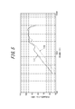
- FIG. 5 is a diagram illustrating frequency characteristics related to the sound pressure of the electronic apparatus 1 according to the first embodiment.
- the frequency characteristic 170 when the buffer material 90 is not disposed between the display unit 20 and the sheet metal 80 and the frequency when the buffer material 90 is disposed between the display unit 20 and the sheet metal 80.
- Each characteristic 171 is shown.
- the horizontal axis represents frequency [Hz]
- the vertical axis represents A characteristic sound pressure level [dBA].
- the sound pressure level is increased by about 5 to 10 [dBA] due to the arrangement of the buffer material 90.
- FIG. 6 is a diagram illustrating a frequency characteristic related to a distortion factor of the electronic device 1 according to the first embodiment.
- the distortion rate represents the degree of distortion of the vibration waveform and is defined as the ratio of harmonics to the fundamental wave. The smaller the distortion rate, the smaller the ratio of harmonics to the fundamental wave and the better the sound quality.
- the frequency characteristic 180 when the buffer material 90 is not disposed between the display unit 20 and the sheet metal 80 and the frequency when the buffer material 90 is disposed between the display unit 20 and the sheet metal 80.
- Each characteristic 181 is shown.
- the horizontal axis represents frequency [Hz]
- the vertical axis represents distortion rate [%]. As shown in FIG. 6, for example, in the frequency band of 300 to 1000 [Hz], the distortion rate is reduced by about 4 to 24 [%] due to the arrangement of the buffer material 90.
- the panel 10 is deformed due to the deformation of the piezoelectric element 30 attached to the back surface of the panel 10, and the longitudinal direction in which the piezoelectric element 30 is bonded. Sufficiently vibrates from one end side to the vicinity of the center. Therefore, the user brings a part of the user's body (for example, cartilage of the outer ear) into contact with at least a part of the upper region from the center of the panel 10, thereby causing air conduction sound and vibration due to vibration of the panel 10. I can hear the sound.
- a part of the user's body for example, cartilage of the outer ear
- the display unit 20 and the piezoelectric element 30 are joined to the panel 10 by the joining member 70.
- the piezoelectric element 30 can be attached to the panel 10 in a state in which the degree of freedom of deformation of the piezoelectric element 30 is hardly hindered.
- the joining member 70 can be a non-heating type curable adhesive. Accordingly, there is an advantage that thermal stress shrinkage hardly occurs between the display unit 20 and the piezoelectric element 30 and the panel 10 at the time of curing.
- the joining member 70 can be a double-sided tape. Thereby, there exists an advantage that the shrinkage stress like the time of use of an adhesive agent is hard to apply between the display part 20 and the piezoelectric element 30, and the panel 10. FIG. Further, since the panel 10 is also joined to the housing 60 by the joining member 70, the same effect can be obtained.
- a buffer material 90 is disposed between the display unit 20 and the sheet metal 80.
- the display part 20 which carries out a curved vibration with the vibration of the piezoelectric element 30 interferes with the sheet metal 80. Therefore, it is possible to reduce a decrease in sound pressure and an increase in distortion caused by the vibration of the panel 10. Since the interference between the display unit 20 and the sheet metal 80 can be suppressed or reduced, the gap between the display unit 20 and the sheet metal 80 can be reduced, and the electronic device 1 can be thinned.
- both the piezoelectric element 30 and the buffer material 90 are disposed on one end side in one direction in a plan view of the panel 10. Since the region (main vibration part) of the panel 10 to which the piezoelectric element 30 is attached vibrates most greatly, the display unit 20, the sheet metal 80, and the plate member 80 are efficiently arranged by arranging the cushioning material 90 on the same side as the piezoelectric element 30. Interference can be suppressed or reduced.
- the cushioning material 90 is bonded only to the display unit 20 and is only in contact with the sheet metal 80.
- the cushioning material 90 is bonded only to the display unit 20 and is only in contact with the sheet metal 80.
- the front case 61 includes a sheet metal 80 as an insert member.
- the sheet metal 80 can reduce the thickness while maintaining the strength of the electronic device 1.
- the buffer material 90 is disposed outside the end portion in the longitudinal direction of the piezoelectric element 30. Since main vibration, which is large vibration, is generated on the inner side of the end portion of the piezoelectric element 30, the buffer material 90 is disposed on the outer side, so that it is possible to reduce the obstruction of desired vibration more than necessary.
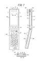
- FIG. 7 is a diagram illustrating a mounting structure of the electronic device 1 according to the second embodiment.
- 7 (a) is a front view
- FIG. 7 (b) is a cross-sectional view taken along line bb in FIG. 7 (a)
- FIG. 7 (c) is taken along line cc in FIG. 7 (a). It is sectional drawing.
- the electronic device 1 shown in FIG. 7 includes a folding panel in which a cover panel (acrylic plate) that protects the display unit 20 is disposed as a panel 10 on the front surface of the upper housing 60a, and the input unit 40 is disposed on the lower housing 60b.
- Mobile phone terminal is a folding panel in which a cover panel (acrylic plate) that protects the display unit 20 is disposed as a panel 10 on the front surface of the upper housing 60a, and the input unit 40 is disposed on the lower housing 60b.
- the display unit 20, the piezoelectric element 30, and the circuit board 130 are disposed in the recess 65 of the housing 60a.
- the piezoelectric element 30 and the reinforcing member 100 that are visible between the two cushioning materials 90 are omitted for clarity of the drawing.
- the reinforcing member 100 is disposed between the panel 10 and the piezoelectric element 30.
- the reinforcing member 100 is a resin plate including, for example, a resin plate, sheet metal, or glass fiber. That is, the electronic device 1 according to the second embodiment has a structure in which the piezoelectric element 30 and the reinforcing member 100 are bonded by the bonding member 70, and the reinforcing member 100 and the panel 10 are bonded by the bonding member 70.
- the display unit 20 is not bonded to the panel 10 but is supported by the housing 60a. That is, the electronic device 1 according to the second embodiment has a structure in which the display unit 20 is separated from the panel 10 and the display unit 20 and the housing 60a are coupled via the circuit board 130.
- the housing 60a can be configured to include a sheet metal, similarly to the front case 61 of the first embodiment.
- a cushioning material 90 similar to that of the first embodiment is disposed between the panel 10 and the display unit 20 (housing 60a).
- the panel 10 and the cushioning material 90 are joined via the joining member 70, and the display unit 20 and the cushioning material 90 are in contact without going through the joining member.
- the panel 10 and the cushioning material 90 may contact each other without a joining member, and the display unit 20 and the cushioning material 90 may be joined via the joining member.
- FIG. 8 is a diagram illustrating an example of vibration of the panel 10 of the electronic device 1 according to the second embodiment.
- the panel 10 is an acrylic plate having a lower rigidity than the glass plate, and the display unit 20 is not bonded to the back surface of the panel 10.
- the amplitude generated by the piezoelectric element 30 is increased.
- the panel 10 vibrates not only in the attachment region to which the piezoelectric element 30 is attached, but also in a region away from the attachment region. For this reason, the user can hear the vibration sound by bringing his / her ear into contact with an arbitrary position of the panel 10 in addition to the air conduction sound through the air.
- the reinforcing member 100 and the panel 10 are deformed due to the deformation of the piezoelectric element 30 attached to the panel 10 via the reinforcing member 100, and the deformation is performed.
- the air conduction sound and the vibration sound are transmitted to the object in contact with the panel 10.
- the piezoelectric element 30 is attached to the surface of the panel 10 on the inner side of the housing 60a. For this reason, air conduction sound and vibration sound can be transmitted to the user without causing the vibrating body to protrude from the outer surface of the housing 60a.
- the panel 10 is deformed to transmit air conduction sound and vibration sound not only in the attachment region to which the piezoelectric element 30 is attached, but also in any part of the panel 10. For this reason, the user can hear the vibration sound by bringing his / her ear into contact with an arbitrary position of the panel 10 in addition to the air conduction sound through the air.
- the reinforcing member 100 by arranging the reinforcing member 100 between the piezoelectric element 30 and the panel 10, for example, when an external force is applied to the panel 10, the external force is transmitted to the piezoelectric element 30 and the piezoelectric element 30 is The possibility of breakage can be reduced. Moreover, even if the panel 10 is brought into strong contact with the human body, the vibration of the panel 10 can be hardly attenuated. In addition, by disposing the reinforcing member 100 between the piezoelectric element 30 and the panel 10, the resonance frequency of the panel 10 is lowered, and the acoustic characteristics in the low frequency band are improved. Instead of the reinforcing member 100, a plate-like weight may be attached to the piezoelectric element 30 by the joining member 70.
- a cushioning material 90 is disposed between the panel 10 and the display unit 20. Thereby, it can reduce that the panel 10 which carries out a curved vibration with the vibration of the piezoelectric element 30 interferes with the display part 20.
- the cushioning material 90 is adhered only to the panel 10 and is only in contact with the display unit 20.
- the cushioning material 90 is adhered only to both the panel 10 and the display unit 20, it is possible to prevent generation of tension via the cushioning material 90 between the panel 10 and the display unit 20, and the bending vibration of the panel 10 is more than necessary. Inhibition can be reduced.
- the piezoelectric element 30 may be disposed at the center of the panel 10.
- the vibration of the piezoelectric element 30 is evenly transmitted to the entire panel 10 to improve the quality of the air conduction sound, and the user can listen to various positions of the panel 10. The vibration sound can be recognized even if it is touched.
- a plurality of piezoelectric elements 30 may be mounted.
- the piezoelectric element 30 is attached to the panel 10, but may be attached to a location different from the panel 10.
- the piezoelectric element 30 may be attached to a rear case 62 that is attached to the housing 60 and covers the battery 150. Since the rear case 62 is often attached to a surface different from the panel 10 in the electronic device 1 such as a mobile phone terminal, according to such a configuration, the user can place a part of the body (for example, an ear on the surface different from the panel 10). ) To hear the sound.
- the cushioning material 90 is disposed between the rear case 62 that bends and vibrates by the piezoelectric element 30 and a portion that can contact the rear case 62 (for example, the battery 150).
- the panel 10 can constitute a part or all of any of a display panel, an operation panel, a cover panel, and a lid panel for making the rechargeable battery removable.
- the piezoelectric element 30 is disposed outside the display area for the display function.
- the operation panel includes the touch panel of the first embodiment.
- the operation panel includes a sheet key that is a member that constitutes one surface of the operation unit side body, in which, for example, a key top of an operation key is integrally formed in a foldable mobile phone terminal.
- the bonding member for bonding the panel 10 and the piezoelectric element 30 and the bonding member for bonding the panel 10 and the housing 60 (60a) have the same reference numerals.
- the bonding member 70 has been described.
- the joining member used in the first embodiment and the second embodiment may be appropriately different depending on the member to be joined.
Landscapes
- Physics & Mathematics (AREA)
- Acoustics & Sound (AREA)
- Engineering & Computer Science (AREA)
- Signal Processing (AREA)
- Piezo-Electric Transducers For Audible Bands (AREA)
- Telephone Set Structure (AREA)
- Diaphragms For Electromechanical Transducers (AREA)
- Details Of Audible-Bandwidth Transducers (AREA)
Abstract
La présente invention concerne un dispositif électronique qui permet de minimiser efficacement une diminution de la pression acoustique et une augmentation de la distorsion. Le dispositif est équipé d'un élément piézoélectrique (30), d'un panneau (10) supportant l'élément piézoélectrique (30), et d'un châssis (60) servant à maintenir le panneau (10). Dans ce dispositif électronique (1) dans lequel le son conduit par l'air et le son de vibrations transmis par des vibrations d'une partie du corps sont générés par le panneau (10), des matériaux d'amortissement (90) sont disposés entre le panneau (10) et le châssis (60).
Priority Applications (2)
| Application Number | Priority Date | Filing Date | Title |
|---|---|---|---|
| US14/361,823 US9197966B2 (en) | 2012-05-14 | 2013-05-14 | Electronic device |
| EP13791560.9A EP2811721B1 (fr) | 2012-05-14 | 2013-05-14 | Dispositif électronique |
Applications Claiming Priority (2)
| Application Number | Priority Date | Filing Date | Title |
|---|---|---|---|
| JP2012-110951 | 2012-05-14 | ||
| JP2012110951A JP6092526B2 (ja) | 2012-05-14 | 2012-05-14 | 電子機器 |
Publications (1)
| Publication Number | Publication Date |
|---|---|
| WO2013172018A1 true WO2013172018A1 (fr) | 2013-11-21 |
Family
ID=49583446
Family Applications (1)
| Application Number | Title | Priority Date | Filing Date |
|---|---|---|---|
| PCT/JP2013/003070 WO2013172018A1 (fr) | 2012-05-14 | 2013-05-14 | Dispositif électronique |
Country Status (4)
| Country | Link |
|---|---|
| US (1) | US9197966B2 (fr) |
| EP (1) | EP2811721B1 (fr) |
| JP (1) | JP6092526B2 (fr) |
| WO (1) | WO2013172018A1 (fr) |
Cited By (3)
| Publication number | Priority date | Publication date | Assignee | Title |
|---|---|---|---|---|
| WO2015136399A1 (fr) * | 2014-03-13 | 2015-09-17 | Semiconductor Energy Laboratory Co., Ltd. | Dispositif électronique |
| US9197966B2 (en) | 2012-05-14 | 2015-11-24 | Kyocera Corporation | Electronic device |
| CN106210376A (zh) * | 2016-07-29 | 2016-12-07 | 努比亚技术有限公司 | 移动终端、振动提示控制装置及方法 |
Families Citing this family (12)
| Publication number | Priority date | Publication date | Assignee | Title |
|---|---|---|---|---|
| JP6075592B2 (ja) * | 2012-05-22 | 2017-02-08 | 京セラ株式会社 | 電子機器 |
| JP5852635B2 (ja) * | 2013-12-24 | 2016-02-03 | 京セラ株式会社 | 電子機器 |
| JP2015126283A (ja) * | 2013-12-25 | 2015-07-06 | 京セラ株式会社 | サファイアパネルおよびそれを用いた携帯端末 |
| JP5856199B2 (ja) * | 2014-02-07 | 2016-02-09 | 京セラ株式会社 | 電子機器 |
| WO2015173686A1 (fr) | 2014-05-16 | 2015-11-19 | Semiconductor Energy Laboratory Co., Ltd. | Dispositif électronique avec batterie secondaire |
| CN110233210B (zh) | 2014-05-16 | 2022-04-26 | 株式会社半导体能源研究所 | 具有二次电池的电子设备 |
| US11108105B2 (en) | 2015-01-22 | 2021-08-31 | Semiconductor Energy Laboratory Co., Ltd. | Secondary battery and electronic device |
| KR102663406B1 (ko) | 2016-04-04 | 2024-05-14 | 엘지디스플레이 주식회사 | 패널 진동형 음향 발생 액츄에이터 및 그를 포함하는 양면 표시 장치 |
| KR20170114471A (ko) | 2016-04-05 | 2017-10-16 | 엘지디스플레이 주식회사 | 유기발광 표시 장치 |
| US10237656B2 (en) | 2016-03-28 | 2019-03-19 | Lg Display Co., Ltd. | Panel vibration type sound generating display device |
| KR101704517B1 (ko) | 2016-03-28 | 2017-02-09 | 엘지디스플레이 주식회사 | 패널 진동형 음향 발생 표시 장치 |
| US11249716B2 (en) * | 2018-12-11 | 2022-02-15 | Samsung Display Co., Ltd. | Display device and method for driving the same |
Citations (5)
| Publication number | Priority date | Publication date | Assignee | Title |
|---|---|---|---|---|
| JP2004336403A (ja) * | 2003-05-08 | 2004-11-25 | Citizen Electronics Co Ltd | パネル型スピーカ付き表示端末装置 |
| JP2005209868A (ja) * | 2004-01-22 | 2005-08-04 | Casio Comput Co Ltd | 電子機器 |
| JP2005348193A (ja) | 2004-06-04 | 2005-12-15 | Nec Tokin Corp | 受話器 |
| JP2009246819A (ja) * | 2008-03-31 | 2009-10-22 | Fujitsu Ltd | 携帯端末装置 |
| JP2010211185A (ja) * | 2009-02-10 | 2010-09-24 | Nec Lcd Technologies Ltd | 液晶表示装置 |
Family Cites Families (16)
| Publication number | Priority date | Publication date | Assignee | Title |
|---|---|---|---|---|
| US7214424B2 (en) * | 1999-03-01 | 2007-05-08 | Nitto Denko Corporation | Heat-peelable pressure-sensitive adhesive sheet |
| US7616771B2 (en) * | 2001-04-27 | 2009-11-10 | Virginia Commonwealth University | Acoustic coupler for skin contact hearing enhancement devices |
| JP3994086B2 (ja) | 2001-06-21 | 2007-10-17 | 1...リミテッド | スピーカ |
| EP2204688B1 (fr) * | 2002-09-03 | 2011-10-26 | Sharp Kabushiki Kaisha | Dispositif d'affichage à cristaux liquides comportant une fonction de sortie sonore et analogue et dispositif éléctronique l'utilisant |
| JP2006333021A (ja) * | 2005-05-25 | 2006-12-07 | Citizen Electronics Co Ltd | パネル型スピーカ付き表示装置 |
| US7565949B2 (en) * | 2005-09-27 | 2009-07-28 | Casio Computer Co., Ltd. | Flat panel display module having speaker function |
| JP2007300426A (ja) | 2006-04-28 | 2007-11-15 | Sony Corp | 圧電振動子およびこれを備えた圧電振動発生装置 |
| JP4882113B2 (ja) * | 2007-11-02 | 2012-02-22 | Necカシオモバイルコミュニケーションズ株式会社 | 筐体のバイブレータ構造、及び携帯電子機器 |
| US20100278362A1 (en) * | 2007-12-20 | 2010-11-04 | Kim David K J | Method and apparatus to interchange between bone conductive and normal mode in receiver |
| US20100225600A1 (en) * | 2009-03-09 | 2010-09-09 | Motorola Inc. | Display Structure with Direct Piezoelectric Actuation |
| JP5214801B2 (ja) * | 2009-04-06 | 2013-06-19 | シャープ株式会社 | 導電性緩衝材および表示装置 |
| TWI409732B (zh) * | 2010-02-23 | 2013-09-21 | Anica Corp | 可撓式顯示器 |
| US9007320B2 (en) | 2010-10-27 | 2015-04-14 | Kyocera Corporation | Electronic equipment and mobile terminal provided with same |
| US20130328820A1 (en) * | 2011-02-23 | 2013-12-12 | Kyocera Corporation | Electronic device |
| JP6092526B2 (ja) | 2012-05-14 | 2017-03-08 | 京セラ株式会社 | 電子機器 |
| WO2014003148A1 (fr) | 2012-06-27 | 2014-01-03 | 京セラ株式会社 | Dispositif électronique, procédé de commande et programme de commande |
-
2012
- 2012-05-14 JP JP2012110951A patent/JP6092526B2/ja not_active Expired - Fee Related
-
2013
- 2013-05-14 WO PCT/JP2013/003070 patent/WO2013172018A1/fr active Application Filing
- 2013-05-14 EP EP13791560.9A patent/EP2811721B1/fr active Active
- 2013-05-14 US US14/361,823 patent/US9197966B2/en active Active
Patent Citations (5)
| Publication number | Priority date | Publication date | Assignee | Title |
|---|---|---|---|---|
| JP2004336403A (ja) * | 2003-05-08 | 2004-11-25 | Citizen Electronics Co Ltd | パネル型スピーカ付き表示端末装置 |
| JP2005209868A (ja) * | 2004-01-22 | 2005-08-04 | Casio Comput Co Ltd | 電子機器 |
| JP2005348193A (ja) | 2004-06-04 | 2005-12-15 | Nec Tokin Corp | 受話器 |
| JP2009246819A (ja) * | 2008-03-31 | 2009-10-22 | Fujitsu Ltd | 携帯端末装置 |
| JP2010211185A (ja) * | 2009-02-10 | 2010-09-24 | Nec Lcd Technologies Ltd | 液晶表示装置 |
Non-Patent Citations (1)
| Title |
|---|
| See also references of EP2811721A4 * |
Cited By (9)
| Publication number | Priority date | Publication date | Assignee | Title |
|---|---|---|---|---|
| US9197966B2 (en) | 2012-05-14 | 2015-11-24 | Kyocera Corporation | Electronic device |
| WO2015136399A1 (fr) * | 2014-03-13 | 2015-09-17 | Semiconductor Energy Laboratory Co., Ltd. | Dispositif électronique |
| US9594402B2 (en) | 2014-03-13 | 2017-03-14 | Semiconductor Energy Laboratory Co., Ltd. | Electronic device |
| US10289158B2 (en) | 2014-03-13 | 2019-05-14 | Semiconductor Energy Laboratory Co., Ltd. | Electronic device |
| US11054858B2 (en) | 2014-03-13 | 2021-07-06 | Semiconductor Energy Laboratory Co., Ltd. | Electronic device |
| US11531372B2 (en) | 2014-03-13 | 2022-12-20 | Semiconductor Energy Laboratory Co., Ltd. | Electronic device |
| US11762423B2 (en) | 2014-03-13 | 2023-09-19 | Semiconductor Energy Laboratory Co., Ltd. | Electronic device |
| CN106210376A (zh) * | 2016-07-29 | 2016-12-07 | 努比亚技术有限公司 | 移动终端、振动提示控制装置及方法 |
| CN106210376B (zh) * | 2016-07-29 | 2020-05-19 | 瑞安市辉煌网络科技有限公司 | 移动终端、振动提示控制装置及方法 |
Also Published As
| Publication number | Publication date |
|---|---|
| EP2811721B1 (fr) | 2020-07-01 |
| JP6092526B2 (ja) | 2017-03-08 |
| EP2811721A1 (fr) | 2014-12-10 |
| US20150078588A1 (en) | 2015-03-19 |
| EP2811721A4 (fr) | 2015-09-30 |
| JP2013239857A (ja) | 2013-11-28 |
| US9197966B2 (en) | 2015-11-24 |
Similar Documents
| Publication | Publication Date | Title |
|---|---|---|
| JP5856196B2 (ja) | 電子機器 | |
| JP5818923B2 (ja) | 電子機器 | |
| JP5812925B2 (ja) | 電子機器 | |
| JP6092526B2 (ja) | 電子機器 | |
| JP5734473B2 (ja) | 電子機器 | |
| JP5818922B2 (ja) | 電子機器 | |
| JP5969817B2 (ja) | 電子機器 | |
| JP5972042B2 (ja) | 電子機器 | |
| JP5968018B2 (ja) | 電子機器 | |
| JP5968050B2 (ja) | 電子機器 | |
| JP6022211B2 (ja) | 電子機器 | |
| WO2013175780A1 (fr) | Équipement électronique et procédé de commande d'équipement électronique | |
| JP5856199B2 (ja) | 電子機器 | |
| JP2015050703A (ja) | 電子機器 | |
| JP6073074B2 (ja) | 電子機器 | |
| JP5900986B2 (ja) | 電子機器 | |
| JP5957279B2 (ja) | 電子機器 | |
| JP2013243505A (ja) | 電子機器 |
Legal Events
| Date | Code | Title | Description |
|---|---|---|---|
| 121 | Ep: the epo has been informed by wipo that ep was designated in this application |
Ref document number: 13791560 Country of ref document: EP Kind code of ref document: A1 |
|
| WWE | Wipo information: entry into national phase |
Ref document number: 14361823 Country of ref document: US |
|
| WWE | Wipo information: entry into national phase |
Ref document number: 2013791560 Country of ref document: EP |
|
| NENP | Non-entry into the national phase |
Ref country code: DE |