WO2013141231A1 - タンタルスパッタリングターゲット及びその製造方法並びに同ターゲットを用いて形成した半導体配線用バリア膜 - Google Patents
タンタルスパッタリングターゲット及びその製造方法並びに同ターゲットを用いて形成した半導体配線用バリア膜 Download PDFInfo
- Publication number
- WO2013141231A1 WO2013141231A1 PCT/JP2013/057790 JP2013057790W WO2013141231A1 WO 2013141231 A1 WO2013141231 A1 WO 2013141231A1 JP 2013057790 W JP2013057790 W JP 2013057790W WO 2013141231 A1 WO2013141231 A1 WO 2013141231A1
- Authority
- WO
- WIPO (PCT)
- Prior art keywords
- target
- variation
- heat
- tantalum
- treated
- Prior art date
Links
- 229910052715 tantalum Inorganic materials 0.000 title claims abstract description 62
- GUVRBAGPIYLISA-UHFFFAOYSA-N tantalum atom Chemical compound [Ta] GUVRBAGPIYLISA-UHFFFAOYSA-N 0.000 title claims abstract description 62
- 238000005477 sputtering target Methods 0.000 title claims abstract description 19
- 238000000034 method Methods 0.000 title claims description 23
- 230000004888 barrier function Effects 0.000 title claims description 12
- 239000004065 semiconductor Substances 0.000 title claims description 11
- 238000004519 manufacturing process Methods 0.000 title description 6
- 239000013078 crystal Substances 0.000 claims abstract description 49
- 238000010438 heat treatment Methods 0.000 claims description 36
- 238000010894 electron beam technology Methods 0.000 claims description 19
- 239000002994 raw material Substances 0.000 claims description 19
- 238000005096 rolling process Methods 0.000 claims description 10
- 238000005266 casting Methods 0.000 claims description 6
- 238000002844 melting Methods 0.000 claims description 3
- 230000008018 melting Effects 0.000 claims description 3
- 239000012528 membrane Substances 0.000 abstract 2
- 239000010408 film Substances 0.000 description 51
- 238000005242 forging Methods 0.000 description 45
- 239000010409 thin film Substances 0.000 description 40
- 235000012431 wafers Nutrition 0.000 description 24
- XUIMIQQOPSSXEZ-UHFFFAOYSA-N Silicon Chemical compound [Si] XUIMIQQOPSSXEZ-UHFFFAOYSA-N 0.000 description 16
- 229910052710 silicon Inorganic materials 0.000 description 16
- 239000010703 silicon Substances 0.000 description 16
- 238000004544 sputter deposition Methods 0.000 description 16
- 238000012545 processing Methods 0.000 description 12
- 230000000052 comparative effect Effects 0.000 description 11
- 238000005097 cold rolling Methods 0.000 description 5
- RYGMFSIKBFXOCR-UHFFFAOYSA-N Copper Chemical compound [Cu] RYGMFSIKBFXOCR-UHFFFAOYSA-N 0.000 description 3
- 230000015572 biosynthetic process Effects 0.000 description 3
- 238000010273 cold forging Methods 0.000 description 3
- 229910052802 copper Inorganic materials 0.000 description 3
- 239000010949 copper Substances 0.000 description 3
- 230000010354 integration Effects 0.000 description 3
- 238000005070 sampling Methods 0.000 description 3
- 238000010586 diagram Methods 0.000 description 2
- 239000007769 metal material Substances 0.000 description 2
- 238000000137 annealing Methods 0.000 description 1
- 230000007423 decrease Effects 0.000 description 1
- 230000007547 defect Effects 0.000 description 1
- 230000000593 degrading effect Effects 0.000 description 1
- 238000009792 diffusion process Methods 0.000 description 1
- 238000004090 dissolution Methods 0.000 description 1
- 230000000694 effects Effects 0.000 description 1
- 230000003628 erosive effect Effects 0.000 description 1
- 238000011156 evaluation Methods 0.000 description 1
- 230000002349 favourable effect Effects 0.000 description 1
- 238000003384 imaging method Methods 0.000 description 1
- 239000011229 interlayer Substances 0.000 description 1
- 239000010410 layer Substances 0.000 description 1
- 238000003754 machining Methods 0.000 description 1
- 239000000463 material Substances 0.000 description 1
- 238000012986 modification Methods 0.000 description 1
- 230000004048 modification Effects 0.000 description 1
- 230000003287 optical effect Effects 0.000 description 1
- 239000002245 particle Substances 0.000 description 1
- 238000005498 polishing Methods 0.000 description 1
- 239000011148 porous material Substances 0.000 description 1
- 238000001953 recrystallisation Methods 0.000 description 1
- 238000011160 research Methods 0.000 description 1
- 238000005204 segregation Methods 0.000 description 1
- 238000009721 upset forging Methods 0.000 description 1
Images

Classifications
-
- C—CHEMISTRY; METALLURGY
- C23—COATING METALLIC MATERIAL; COATING MATERIAL WITH METALLIC MATERIAL; CHEMICAL SURFACE TREATMENT; DIFFUSION TREATMENT OF METALLIC MATERIAL; COATING BY VACUUM EVAPORATION, BY SPUTTERING, BY ION IMPLANTATION OR BY CHEMICAL VAPOUR DEPOSITION, IN GENERAL; INHIBITING CORROSION OF METALLIC MATERIAL OR INCRUSTATION IN GENERAL
- C23C—COATING METALLIC MATERIAL; COATING MATERIAL WITH METALLIC MATERIAL; SURFACE TREATMENT OF METALLIC MATERIAL BY DIFFUSION INTO THE SURFACE, BY CHEMICAL CONVERSION OR SUBSTITUTION; COATING BY VACUUM EVAPORATION, BY SPUTTERING, BY ION IMPLANTATION OR BY CHEMICAL VAPOUR DEPOSITION, IN GENERAL
- C23C14/00—Coating by vacuum evaporation, by sputtering or by ion implantation of the coating forming material
- C23C14/22—Coating by vacuum evaporation, by sputtering or by ion implantation of the coating forming material characterised by the process of coating
- C23C14/34—Sputtering
- C23C14/3407—Cathode assembly for sputtering apparatus, e.g. Target
- C23C14/3414—Metallurgical or chemical aspects of target preparation, e.g. casting, powder metallurgy
-
- B—PERFORMING OPERATIONS; TRANSPORTING
- B22—CASTING; POWDER METALLURGY
- B22D—CASTING OF METALS; CASTING OF OTHER SUBSTANCES BY THE SAME PROCESSES OR DEVICES
- B22D21/00—Casting non-ferrous metals or metallic compounds so far as their metallurgical properties are of importance for the casting procedure; Selection of compositions therefor
- B22D21/06—Casting non-ferrous metals with a high melting point, e.g. metallic carbides
-
- C—CHEMISTRY; METALLURGY
- C22—METALLURGY; FERROUS OR NON-FERROUS ALLOYS; TREATMENT OF ALLOYS OR NON-FERROUS METALS
- C22C—ALLOYS
- C22C27/00—Alloys based on rhenium or a refractory metal not mentioned in groups C22C14/00 or C22C16/00
- C22C27/02—Alloys based on vanadium, niobium, or tantalum
-
- C—CHEMISTRY; METALLURGY
- C22—METALLURGY; FERROUS OR NON-FERROUS ALLOYS; TREATMENT OF ALLOYS OR NON-FERROUS METALS
- C22F—CHANGING THE PHYSICAL STRUCTURE OF NON-FERROUS METALS AND NON-FERROUS ALLOYS
- C22F1/00—Changing the physical structure of non-ferrous metals or alloys by heat treatment or by hot or cold working
- C22F1/16—Changing the physical structure of non-ferrous metals or alloys by heat treatment or by hot or cold working of other metals or alloys based thereon
- C22F1/18—High-melting or refractory metals or alloys based thereon
-
- C—CHEMISTRY; METALLURGY
- C23—COATING METALLIC MATERIAL; COATING MATERIAL WITH METALLIC MATERIAL; CHEMICAL SURFACE TREATMENT; DIFFUSION TREATMENT OF METALLIC MATERIAL; COATING BY VACUUM EVAPORATION, BY SPUTTERING, BY ION IMPLANTATION OR BY CHEMICAL VAPOUR DEPOSITION, IN GENERAL; INHIBITING CORROSION OF METALLIC MATERIAL OR INCRUSTATION IN GENERAL
- C23C—COATING METALLIC MATERIAL; COATING MATERIAL WITH METALLIC MATERIAL; SURFACE TREATMENT OF METALLIC MATERIAL BY DIFFUSION INTO THE SURFACE, BY CHEMICAL CONVERSION OR SUBSTITUTION; COATING BY VACUUM EVAPORATION, BY SPUTTERING, BY ION IMPLANTATION OR BY CHEMICAL VAPOUR DEPOSITION, IN GENERAL
- C23C14/00—Coating by vacuum evaporation, by sputtering or by ion implantation of the coating forming material
- C23C14/06—Coating by vacuum evaporation, by sputtering or by ion implantation of the coating forming material characterised by the coating material
- C23C14/14—Metallic material, boron or silicon
-
- H—ELECTRICITY
- H01—ELECTRIC ELEMENTS
- H01J—ELECTRIC DISCHARGE TUBES OR DISCHARGE LAMPS
- H01J37/00—Discharge tubes with provision for introducing objects or material to be exposed to the discharge, e.g. for the purpose of examination or processing thereof
- H01J37/32—Gas-filled discharge tubes
- H01J37/34—Gas-filled discharge tubes operating with cathodic sputtering
- H01J37/3411—Constructional aspects of the reactor
- H01J37/3414—Targets
- H01J37/3426—Material
-
- H—ELECTRICITY
- H01—ELECTRIC ELEMENTS
- H01L—SEMICONDUCTOR DEVICES NOT COVERED BY CLASS H10
- H01L21/00—Processes or apparatus adapted for the manufacture or treatment of semiconductor or solid state devices or of parts thereof
- H01L21/02—Manufacture or treatment of semiconductor devices or of parts thereof
- H01L21/02104—Forming layers
- H01L21/02365—Forming inorganic semiconducting materials on a substrate
- H01L21/02612—Formation types
- H01L21/02617—Deposition types
- H01L21/02631—Physical deposition at reduced pressure, e.g. MBE, sputtering, evaporation
-
- H—ELECTRICITY
- H01—ELECTRIC ELEMENTS
- H01J—ELECTRIC DISCHARGE TUBES OR DISCHARGE LAMPS
- H01J2237/00—Discharge tubes exposing object to beam, e.g. for analysis treatment, etching, imaging
- H01J2237/32—Processing objects by plasma generation
- H01J2237/33—Processing objects by plasma generation characterised by the type of processing
- H01J2237/332—Coating
-
- H—ELECTRICITY
- H01—ELECTRIC ELEMENTS
- H01L—SEMICONDUCTOR DEVICES NOT COVERED BY CLASS H10
- H01L21/00—Processes or apparatus adapted for the manufacture or treatment of semiconductor or solid state devices or of parts thereof
- H01L21/02—Manufacture or treatment of semiconductor devices or of parts thereof
- H01L21/04—Manufacture or treatment of semiconductor devices or of parts thereof the devices having potential barriers, e.g. a PN junction, depletion layer or carrier concentration layer
- H01L21/18—Manufacture or treatment of semiconductor devices or of parts thereof the devices having potential barriers, e.g. a PN junction, depletion layer or carrier concentration layer the devices having semiconductor bodies comprising elements of Group IV of the Periodic Table or AIIIBV compounds with or without impurities, e.g. doping materials
- H01L21/28—Manufacture of electrodes on semiconductor bodies using processes or apparatus not provided for in groups H01L21/20 - H01L21/268
- H01L21/283—Deposition of conductive or insulating materials for electrodes conducting electric current
- H01L21/285—Deposition of conductive or insulating materials for electrodes conducting electric current from a gas or vapour, e.g. condensation
- H01L21/28506—Deposition of conductive or insulating materials for electrodes conducting electric current from a gas or vapour, e.g. condensation of conductive layers
- H01L21/28512—Deposition of conductive or insulating materials for electrodes conducting electric current from a gas or vapour, e.g. condensation of conductive layers on semiconductor bodies comprising elements of Group IV of the Periodic Table
- H01L21/2855—Deposition of conductive or insulating materials for electrodes conducting electric current from a gas or vapour, e.g. condensation of conductive layers on semiconductor bodies comprising elements of Group IV of the Periodic Table by physical means, e.g. sputtering, evaporation
-
- H—ELECTRICITY
- H01—ELECTRIC ELEMENTS
- H01L—SEMICONDUCTOR DEVICES NOT COVERED BY CLASS H10
- H01L21/00—Processes or apparatus adapted for the manufacture or treatment of semiconductor or solid state devices or of parts thereof
- H01L21/70—Manufacture or treatment of devices consisting of a plurality of solid state components formed in or on a common substrate or of parts thereof; Manufacture of integrated circuit devices or of parts thereof
- H01L21/71—Manufacture of specific parts of devices defined in group H01L21/70
- H01L21/768—Applying interconnections to be used for carrying current between separate components within a device comprising conductors and dielectrics
- H01L21/76838—Applying interconnections to be used for carrying current between separate components within a device comprising conductors and dielectrics characterised by the formation and the after-treatment of the conductors
- H01L21/76841—Barrier, adhesion or liner layers
- H01L21/76843—Barrier, adhesion or liner layers formed in openings in a dielectric
Definitions
- the present invention relates to a tantalum sputtering target used for forming a barrier film of a copper wiring in a semiconductor device such as an LSI.
- a barrier film made of tantalum or the like under the copper wiring is generally formed by sputtering a tantalum target.
- a tantalum target is usually manufactured by forging, annealing, rolling, heat treatment, finishing, etc., an ingot or billet obtained by melting and casting a tantalum raw material.
- the tantalum target and its manufacturing method the following techniques are known.
- Patent Document 1 discloses that a tantalum target having a crystal structure in which the crystal orientation located at the center plane of the target is (222) preferential is manufactured, thereby improving the crystal orientation structure of the target and performing sputtering. It is described that the film uniformity (uniformity) can be improved, the quality of sputter film formation can be improved, and the production yield can be remarkably improved.
- Patent Document 2 manufactures a tantalum target in which the area ratio of a crystal having any orientation of (100), (111), and (110) does not exceed 0.5 when the total sum of crystal orientations is 1.
- the film formation rate is high, the film uniformity (uniformity) is excellent, the film formation characteristics with less arcing and particle generation are excellent, and the target utilization efficiency is also good.
- Patent Document 3 by using a manufacturing method including a step of clock rolling a metal material, the texture band can be reduced and a uniform fine grain structure can be obtained over the entire surface and thickness of the metal material.
- the true strain applied by forging is about 0.75 to about 2.0.
- the present invention provides a tantalum sputtering target that can further improve the film thickness uniformity of a thin film formed by sputtering and can reduce variations in the resistance value (sheet resistance) of the film.
- the task is to do.
- the present inventors have conducted intensive research, and as a result, by controlling the true strain amount during forging, it is possible to control the variation in the crystal grain size of the target, thereby, It has been found that the uniformity of the film thickness (uniformity) of the thin film formed by sputtering this target can be further improved and the variation in the resistance value (sheet resistance) of the film can be reduced.
- the present invention 1) A tantalum sputtering target, wherein the average crystal grain size of the target is 50 ⁇ m or more and 200 ⁇ m or less, and the variation of the crystal grain size in the target surface is 40% or more and 60% or less, 2) A barrier film for semiconductor wiring formed using the tantalum sputtering target described in 1) above, wherein the sheet resistance Rs variation with respect to the target life is 5.0% or less, and the film thickness uniformity with respect to the target life A barrier film for semiconductor wiring, wherein the variation of 3) An ingot or billet obtained by melting and casting a tantalum material with an electron beam is heat-treated at 900 ° C. to 1400 ° C., then forged, and then heat-treated at 850 ° C.
- a manufacturing method is provided.
- a sputtering target with an extremely uniform crystal grain size can be obtained by controlling the amount of true strain during forging.
- the sputtering target adjusted in this way can remarkably improve the film thickness uniformity with respect to the target life of the thin film formed by sputtering, and also reduces variations in resistance value (sheet resistance) with respect to the target life of the thin film. It has an excellent effect of being able to.
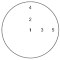
- Example of this invention is a schematic diagram which shows the location which measured the crystal grain diameter of the target.
- Example of this invention and a comparative example it is a schematic diagram which shows the location which measured the sheet resistance value and film thickness of the thin film.
- the tantalum sputtering target of the present invention can be manufactured by the following process. First, high purity tantalum having a purity of 99.99% or more is prepared as a tantalum raw material. Although there is no restriction
- the sputtering target of the present invention can be obtained by performing a heat treatment at a temperature of ° C.-finishing (machining, polishing, etc.).
- the cold forging and the subsequent heat treatment may be performed in one cycle, but may be repeated as necessary.
- cold (hot) rolling and subsequent heat treatment may be performed in one cycle, but may be repeated as necessary.
- Casting structure can be destroyed by forging or rolling, and pores and segregation can be diffused or disappeared. Furthermore, this can be recrystallized by heat treatment, and the target structure can be made dense by repeating this forging or rolling and heat treatment. And miniaturization and the strength of the target can be increased.
- forging is preferably performed so that the true strain is 3.0 or more and 5.0 or less in order to control variation in the average crystal grain size of the target.
- the true strain is calculated from the ratio of the height of the ingot or billet before and after forging. For example, when the thickness of the billet before forging is a and the thickness of the billet after forging is b, the true strain can be calculated by ln (a / b) (ln is a natural logarithm).
- the evaluation is performed by the integrated value ⁇ ln (a / b) of the entire forging process.
- the heat-treated forged product is cold-rolled (hot) at a reduction rate of 80% to 90%.
- the non-recrystallized structure can be eliminated, and the variation in crystal grain size can be adjusted to a desired range.
- the heat treatment after casting on the melt-cast tantalum ingot or billet is performed at a temperature of 900 ° C. to 1400 ° C.
- the heat treatment after rolling is performed at a temperature of 750 ° C. to 1000 ° C. to make the structure fine and uniform. Is desirable.
- the structure of the tantalum sputtering target thus obtained has an average crystal grain size of 50 ⁇ m or more and 200 ⁇ m or less, and the crystal grain size variation in the target plane is 40% or more and 60% or less.
- the present invention can provide a tantalum sputtering target in which the variation in the crystal grain size of the target is controlled.
- the variation in crystal grain size is 40% or more and 60% or less, more preferably 40% or more and 50% or less. If the variation in crystal grain size is too large, the film thickness uniformity and specific resistance variation of the sputtered thin film will deteriorate. Thus, stable sputtering characteristics can be obtained.
- the crystal grain size was measured with an optical microscope using an analytical SIS FIVE (Soft imaging System) on a crystal structure photograph taken with a field of view of 1500 ⁇ m ⁇ 1200 ⁇ m.
- the calculation of the crystal grain size was based on the average grain area method of ASTM, the crystal grain area was converted into a circle, and the diameter of the circle was defined as the crystal grain size.
- the crystal grain size is measured at a total of five locations by sampling one target center, two R (diameter) ⁇ 1/2 points, and two R points (outer periphery). Went.
- the thin film formed by sputtering the target of the present invention has a variation in sheet resistance Rs with respect to the target life of 5.0% or less, more preferably 4.0% or less, and even more preferably 3.0% or less. Further, the variation in sheet resistance Rs is preferably as small as possible, and can be achieved up to about 2.2% in the present invention.
- the target life means the life of the target from the start of use of the target until the thickness of the target decreases due to the progress of erosion due to the sputtering phenomenon and the target cannot be used. This can be expressed as an integration of the power during sputtering and the total sputtering time. For example, at a power of 15 kW, the target life of a target that can be used for 100 hours is 1500 kWh.
- the sheet resistance is 1 at the wafer center, 8 at R (diameter) ⁇ 1/3 point (45 ° interval), 16 at R (diameter) ⁇ 2/3 point (22.5 ° interval), A total of 49 points were measured by sampling 24 points (15 ° intervals) at the R point (outer periphery).
- the thin film formed by sputtering the target of the present invention has a variation in film thickness uniformity with respect to the target life of 5.0% or less, more preferably 4.0% or less, and even more preferably 3.0% or less. . Further, the smaller the variation in film thickness uniformity, the better. In the present invention, it can be achieved up to about 1.2%.
- the film thickness is 1 at the wafer center, 8 at R (diameter) ⁇ 1/3 point (45 ° interval), 16 at R (diameter) ⁇ 2/3 point (22.5 ° interval), A total of 49 points were measured by sampling 24 points (15 ° intervals) at the R point (outer periphery).
- Example 1 A tantalum raw material with a purity of 99.997% was melted with an electron beam and cast into a billet having a thickness of 54 mm and a diameter of 195 mm ⁇ . Then, it heat-processed at 1200 degreeC. Next, the billet was forged at room temperature and then heat-treated at a temperature of 900 ° C. Next, this was forged and upset at room temperature, and again heat treated at a temperature of 900 ° C. Next, this was again forged and upset at room temperature, and heat-treated at a temperature of 900 ° C. As a result of repeatedly performing forging and heat treatment in this way, the integrated value of true strain in the entire forging process was 4.1.
- Example 2 A tantalum raw material with a purity of 99.997% was melted with an electron beam and cast into a billet having a thickness of 54 mm and a diameter of 195 mm ⁇ . Then, it heat-processed at 1100 degreeC. Next, the billet was forged at room temperature and then heat-treated at a temperature of 900 ° C. Next, this was forged and upset at room temperature, and again heat treated at a temperature of 900 ° C. Next, this was again forged and upset at room temperature, and heat-treated at a temperature of 900 ° C. As a result of repeatedly performing forging and heat treatment in this way, the integrated value of true strain in the entire forging process was 4.1.
- Example 3 A tantalum raw material with a purity of 99.997% was melted with an electron beam and cast into a billet having a thickness of 54 mm and a diameter of 195 mm ⁇ . Then, it heat-processed at 1200 degreeC. Next, the billet was forged at room temperature and then heat-treated at a temperature of 900 ° C. Next, this was forged and upset at room temperature, and again heat treated at a temperature of 900 ° C. Next, this was again forged and upset at room temperature, and heat-treated at a temperature of 900 ° C. As a result of repeatedly performing forging and heat treatment in this way, the integrated value of true strain in the entire forging process was 4.0.
- Example 4 A tantalum raw material with a purity of 99.997% was melted with an electron beam and cast into a billet having a thickness of 54 mm and a diameter of 195 mm ⁇ . Then, it heat-processed at 1000 degreeC. Next, the billet was forged at room temperature and then heat-treated at a temperature of 900 ° C. Next, this was forged and upset at room temperature, and again heat treated at a temperature of 900 ° C. Next, this was again forged and upset at room temperature, and heat-treated at a temperature of 900 ° C. As a result of repeatedly performing forging and heat treatment in this manner, the integrated value of true strain in the entire forging process was 4.2.
- Example 5 A tantalum raw material with a purity of 99.997% was melted with an electron beam and cast into a billet having a thickness of 54 mm and a diameter of 195 mm ⁇ . Then, it heat-processed at 1300 degreeC. Next, the billet was forged at room temperature and then heat-treated at a temperature of 900 ° C. Next, this was forged and upset at room temperature, and again heat treated at a temperature of 900 ° C. Next, this was again forged and upset at room temperature, and heat-treated at a temperature of 900 ° C. As a result of repeatedly performing forging and heat treatment in this manner, the integrated value of true strain in the entire forging process was 4.2.
- Example 6 A tantalum raw material with a purity of 99.997% was melted with an electron beam and cast into a billet having a thickness of 54 mm and a diameter of 195 mm ⁇ . Then, it heat-processed at 1350 degreeC. Next, the billet was forged at room temperature and then heat-treated at a temperature of 850 ° C. Next, this was forged and upset at room temperature, and again heat treated at a temperature of 850 ° C. Next, this was again forged and upset at room temperature, and heat-treated at a temperature of 850 ° C. As a result of repeating forging and heat treatment in this way, the integrated value of true strain in the entire forging process was 4.4.
- Example 7 A tantalum raw material with a purity of 99.997% was melted with an electron beam and cast into a billet having a thickness of 54 mm and a diameter of 195 mm ⁇ . Then, it heat-processed at 1200 degreeC. Next, the billet was forged at room temperature and then heat-treated at a temperature of 1250 ° C. Next, this was forged and upset at room temperature, and again heat treated at a temperature of 1100 ° C. Next, this was again forged and upset at room temperature, and heat-treated at a temperature of 1100 ° C. As a result of repeating forging and heat treatment in this way, the integrated value of true strain in the entire forging process was 3.8.
- Example 8 A tantalum raw material with a purity of 99.997% was melted with an electron beam and cast into a billet having a thickness of 54 mm and a diameter of 195 mm ⁇ . Then, it heat-processed at 1200 degreeC. Next, the billet was forged at room temperature and then heat-treated at a temperature of 1000 ° C. Next, this was forged and upset at room temperature, and heat-treated again at a temperature of 1000 ° C. Next, this was again forged and upset at room temperature, and heat-treated at a temperature of 1000 ° C. Next, this was again forged and upset at room temperature, and heat-treated at a temperature of 1000 ° C. Next, this was again forged and upset at room temperature, and heat-treated at a temperature of 1000 ° C.
- the integrated value of true strain in the entire forging process was 3.6.
- it was cold-rolled at a reduction rate of 82%, then heat-treated at 900 ° C., and then subjected to finish processing to obtain a target having a thickness of 10 mm and a diameter of 450 mm ⁇ .
- the target obtained by the above steps was analyzed with an electron microscope, the average crystal grain size was 102.1 ⁇ m, and the variation was 46.3%.
- this target was sputtered to form a tantalum thin film on a silicon wafer (12 inches), and the sheet resistance was measured.
- the sheet resistance Rs variation was 3.1%
- the film thickness uniformity variation was 3.8%, both of which were very small and excellent in uniformity. It was.
- any of Examples 1 to 8 it was confirmed that the variation in the average crystal grain size of the tantalum target was 40% or more and 60% or less. It was found that such a structure has a very important role in making the film thickness and specific resistance uniform.
- the series of forging and heat treatment steps were repeated 3 to 4 times, but the true strain was 3.0 or more and 5.0 or less even once or other than the above. In some cases, good results have been obtained.
- the present invention by controlling the variation in the average crystal grain size of the tantalum sputtering target, it is possible to improve the uniformity of the film thickness and specific resistance of the thin film formed using the target. Therefore, if the target of the present invention is used, it is possible to stably produce fine wiring. It is useful as a tantalum sputtering target used for forming a barrier film for a wiring layer in a semiconductor device.
Landscapes
- Chemical & Material Sciences (AREA)
- Engineering & Computer Science (AREA)
- Mechanical Engineering (AREA)
- Materials Engineering (AREA)
- Metallurgy (AREA)
- Organic Chemistry (AREA)
- Physics & Mathematics (AREA)
- Chemical Kinetics & Catalysis (AREA)
- Computer Hardware Design (AREA)
- Condensed Matter Physics & Semiconductors (AREA)
- General Physics & Mathematics (AREA)
- Manufacturing & Machinery (AREA)
- Microelectronics & Electronic Packaging (AREA)
- Power Engineering (AREA)
- Crystallography & Structural Chemistry (AREA)
- Thermal Sciences (AREA)
- Plasma & Fusion (AREA)
- Analytical Chemistry (AREA)
- Physical Vapour Deposition (AREA)
- Electrodes Of Semiconductors (AREA)
- Optics & Photonics (AREA)
Priority Applications (8)
| Application Number | Priority Date | Filing Date | Title |
|---|---|---|---|
| KR1020147019014A KR101690394B1 (ko) | 2012-03-21 | 2013-03-19 | 탄탈 스퍼터링 타깃의 제조 방법 |
| JP2013521685A JP5324016B1 (ja) | 2012-03-21 | 2013-03-19 | タンタルスパッタリングターゲット及びその製造方法並びに同ターゲットを用いて形成した半導体配線用バリア膜 |
| CN201380015330.1A CN104204282B (zh) | 2012-03-21 | 2013-03-19 | 钽溅射靶及其制造方法以及使用该靶形成的半导体布线用阻挡膜 |
| EP13764344.1A EP2781619A4 (en) | 2012-03-21 | 2013-03-19 | TANTALE SPRAY TARGET, METHOD OF MANUFACTURING THE SAME, AND BARRIER FILM FOR SEMICONDUCTOR WIRING FORMED USING THE TARGET |
| KR1020167035316A KR101882606B1 (ko) | 2012-03-21 | 2013-03-19 | 탄탈 스퍼터링 타깃 및 그 제조 방법 그리고 동 타깃을 사용하여 형성한 반도체 배선용 배리어막 |
| US14/384,749 US9890452B2 (en) | 2012-03-21 | 2013-03-19 | Tantalum sputtering target, method for manufacturing same, and barrier film for semiconductor wiring formed by using target |
| SG11201403330TA SG11201403330TA (en) | 2012-03-21 | 2013-03-19 | Tantalum sputtering target, method for manufacturing same, and barrier film for semiconductor wiring formed by using target |
| IL233564A IL233564A (he) | 2012-03-21 | 2014-07-09 | מתז מטרה טנטאלום, שיטה לייצורו וסרט מחסום עבור חיווט מוליך למחצה המיוצר באמצעות שימוש במטרה |
Applications Claiming Priority (2)
| Application Number | Priority Date | Filing Date | Title |
|---|---|---|---|
| JP2012063157 | 2012-03-21 | ||
| JP2012-063157 | 2012-03-21 |
Publications (1)
| Publication Number | Publication Date |
|---|---|
| WO2013141231A1 true WO2013141231A1 (ja) | 2013-09-26 |
Family
ID=49222688
Family Applications (1)
| Application Number | Title | Priority Date | Filing Date |
|---|---|---|---|
| PCT/JP2013/057790 WO2013141231A1 (ja) | 2012-03-21 | 2013-03-19 | タンタルスパッタリングターゲット及びその製造方法並びに同ターゲットを用いて形成した半導体配線用バリア膜 |
Country Status (9)
| Country | Link |
|---|---|
| US (1) | US9890452B2 (he) |
| EP (1) | EP2781619A4 (he) |
| JP (1) | JP5324016B1 (he) |
| KR (2) | KR101882606B1 (he) |
| CN (1) | CN104204282B (he) |
| IL (1) | IL233564A (he) |
| SG (1) | SG11201403330TA (he) |
| TW (1) | TWI586821B (he) |
| WO (1) | WO2013141231A1 (he) |
Cited By (1)
| Publication number | Priority date | Publication date | Assignee | Title |
|---|---|---|---|---|
| CN106521434A (zh) * | 2016-11-07 | 2017-03-22 | 长沙南方钽铌有限责任公司 | 一种具有择优取向的高纯钽靶材的制备方法 |
Families Citing this family (9)
| Publication number | Priority date | Publication date | Assignee | Title |
|---|---|---|---|---|
| JP5144760B2 (ja) | 2009-05-22 | 2013-02-13 | Jx日鉱日石金属株式会社 | タンタルスパッタリングターゲット |
| SG11201501175TA (en) | 2012-12-19 | 2015-05-28 | Jx Nippon Mining & Metals Corp | Tantalum sputtering target and method for producing same |
| EP2878700B1 (en) | 2012-12-19 | 2021-01-20 | JX Nippon Mining & Metals Corporation | Method for producing tantalum sputtering target |
| US9859104B2 (en) | 2013-03-04 | 2018-01-02 | Jx Nippon Mining & Metals Corporation | Tantalum sputtering target and production method therefor |
| CN105593399B (zh) | 2013-10-01 | 2018-05-25 | 吉坤日矿日石金属株式会社 | 钽溅射靶 |
| US10354846B2 (en) | 2013-11-06 | 2019-07-16 | Jx Nippon Mining & Metals Corporation | Sputtering target-backing plate assembly |
| SG11201704463VA (en) | 2015-05-22 | 2017-07-28 | Jx Nippon Mining & Metals Corp | Tantalum sputtering target, and production method therefor |
| SG11201708112TA (en) | 2015-05-22 | 2017-11-29 | Jx Nippon Mining & Metals Corp | Tantalum sputtering target, and production method therefor |
| CN113909414B (zh) * | 2021-09-30 | 2023-12-29 | 宁波江丰电子材料股份有限公司 | 一种钽靶坯的制备方法 |
Citations (6)
| Publication number | Priority date | Publication date | Assignee | Title |
|---|---|---|---|---|
| JPH06264232A (ja) * | 1993-03-12 | 1994-09-20 | Nikko Kinzoku Kk | Ta製スパッタリングタ−ゲットとその製造方法 |
| JP2004027358A (ja) | 2003-01-10 | 2004-01-29 | Nikko Materials Co Ltd | ターゲットの製造方法及びターゲット |
| WO2005045090A1 (ja) | 2003-11-06 | 2005-05-19 | Nikko Materials Co., Ltd. | タンタルスパッタリングターゲット |
| JP2008532765A (ja) | 2005-02-10 | 2008-08-21 | キャボット コーポレイション | スパッタリングターゲットおよびその製造方法 |
| WO2011018971A1 (ja) * | 2009-08-11 | 2011-02-17 | Jx日鉱日石金属株式会社 | タンタルスパッタリングターゲット |
| WO2011018970A1 (ja) * | 2009-08-11 | 2011-02-17 | Jx日鉱日石金属株式会社 | タンタルスパッタリングターゲット |
Family Cites Families (18)
| Publication number | Priority date | Publication date | Assignee | Title |
|---|---|---|---|---|
| US6348139B1 (en) | 1998-06-17 | 2002-02-19 | Honeywell International Inc. | Tantalum-comprising articles |
| JP2001020065A (ja) | 1999-07-07 | 2001-01-23 | Hitachi Metals Ltd | スパッタリング用ターゲット及びその製造方法ならびに高融点金属粉末材料 |
| US6331233B1 (en) | 2000-02-02 | 2001-12-18 | Honeywell International Inc. | Tantalum sputtering target with fine grains and uniform texture and method of manufacture |
| JP3905301B2 (ja) | 2000-10-31 | 2007-04-18 | 日鉱金属株式会社 | タンタル又はタングステンターゲット−銅合金製バッキングプレート組立体及びその製造方法 |
| US7081148B2 (en) | 2001-09-18 | 2006-07-25 | Praxair S.T. Technology, Inc. | Textured-grain-powder metallurgy tantalum sputter target |
| JP4883546B2 (ja) | 2002-09-20 | 2012-02-22 | Jx日鉱日石金属株式会社 | タンタルスパッタリングターゲットの製造方法 |
| WO2004090193A1 (ja) | 2003-04-01 | 2004-10-21 | Nikko Materials Co., Ltd. | タンタルスパッタリングターゲット及びその製造方法 |
| JP4140553B2 (ja) | 2004-04-28 | 2008-08-27 | 株式会社デンソー | 空気流量測定装置 |
| US8252126B2 (en) * | 2004-05-06 | 2012-08-28 | Global Advanced Metals, Usa, Inc. | Sputter targets and methods of forming same by rotary axial forging |
| EP1942204B1 (en) | 2005-10-04 | 2012-04-25 | JX Nippon Mining & Metals Corporation | Sputtering target |
| WO2007103309A2 (en) * | 2006-03-07 | 2007-09-13 | Cabot Corporation | Methods of producing deformed metal articles |
| JP4974362B2 (ja) * | 2006-04-13 | 2012-07-11 | 株式会社アルバック | Taスパッタリングターゲットおよびその製造方法 |
| JP5144760B2 (ja) | 2009-05-22 | 2013-02-13 | Jx日鉱日石金属株式会社 | タンタルスパッタリングターゲット |
| JP5714506B2 (ja) | 2009-11-17 | 2015-05-07 | 株式会社東芝 | タンタルスパッタリングターゲットおよびタンタルスパッタリングターゲットの製造方法ならびに半導体素子の製造方法 |
| WO2011122317A1 (ja) | 2010-03-29 | 2011-10-06 | Jx日鉱日石金属株式会社 | スパッタリング用タンタル製コイル及び同コイルの加工方法 |
| KR20130037215A (ko) | 2010-08-09 | 2013-04-15 | 제이엑스 닛코 닛세키 킨조쿠 가부시키가이샤 | 탄탈 스퍼터링 타깃 |
| KR20130008089A (ko) | 2010-08-09 | 2013-01-21 | 제이엑스 닛코 닛세키 킨조쿠 가부시키가이샤 | 탄탈 스퍼터링 타깃 |
| EP2719793B1 (en) | 2011-09-30 | 2017-11-08 | JX Nippon Mining & Metals Corporation | Regeneration method for tantalum coil for sputtering |
-
2013
- 2013-03-19 KR KR1020167035316A patent/KR101882606B1/ko active IP Right Grant
- 2013-03-19 SG SG11201403330TA patent/SG11201403330TA/en unknown
- 2013-03-19 CN CN201380015330.1A patent/CN104204282B/zh active Active
- 2013-03-19 EP EP13764344.1A patent/EP2781619A4/en not_active Withdrawn
- 2013-03-19 WO PCT/JP2013/057790 patent/WO2013141231A1/ja active Application Filing
- 2013-03-19 KR KR1020147019014A patent/KR101690394B1/ko active IP Right Grant
- 2013-03-19 JP JP2013521685A patent/JP5324016B1/ja active Active
- 2013-03-19 US US14/384,749 patent/US9890452B2/en active Active
- 2013-03-21 TW TW102110010A patent/TWI586821B/zh active
-
2014
- 2014-07-09 IL IL233564A patent/IL233564A/he active IP Right Grant
Patent Citations (6)
| Publication number | Priority date | Publication date | Assignee | Title |
|---|---|---|---|---|
| JPH06264232A (ja) * | 1993-03-12 | 1994-09-20 | Nikko Kinzoku Kk | Ta製スパッタリングタ−ゲットとその製造方法 |
| JP2004027358A (ja) | 2003-01-10 | 2004-01-29 | Nikko Materials Co Ltd | ターゲットの製造方法及びターゲット |
| WO2005045090A1 (ja) | 2003-11-06 | 2005-05-19 | Nikko Materials Co., Ltd. | タンタルスパッタリングターゲット |
| JP2008532765A (ja) | 2005-02-10 | 2008-08-21 | キャボット コーポレイション | スパッタリングターゲットおよびその製造方法 |
| WO2011018971A1 (ja) * | 2009-08-11 | 2011-02-17 | Jx日鉱日石金属株式会社 | タンタルスパッタリングターゲット |
| WO2011018970A1 (ja) * | 2009-08-11 | 2011-02-17 | Jx日鉱日石金属株式会社 | タンタルスパッタリングターゲット |
Non-Patent Citations (1)
| Title |
|---|
| See also references of EP2781619A4 |
Cited By (1)
| Publication number | Priority date | Publication date | Assignee | Title |
|---|---|---|---|---|
| CN106521434A (zh) * | 2016-11-07 | 2017-03-22 | 长沙南方钽铌有限责任公司 | 一种具有择优取向的高纯钽靶材的制备方法 |
Also Published As
| Publication number | Publication date |
|---|---|
| US20150064056A1 (en) | 2015-03-05 |
| SG11201403330TA (en) | 2014-10-30 |
| TWI586821B (zh) | 2017-06-11 |
| TW201406977A (zh) | 2014-02-16 |
| JPWO2013141231A1 (ja) | 2015-08-03 |
| EP2781619A4 (en) | 2015-10-28 |
| KR20160148063A (ko) | 2016-12-23 |
| JP5324016B1 (ja) | 2013-10-23 |
| KR20140105004A (ko) | 2014-08-29 |
| KR101882606B1 (ko) | 2018-07-26 |
| CN104204282A (zh) | 2014-12-10 |
| EP2781619A1 (en) | 2014-09-24 |
| US9890452B2 (en) | 2018-02-13 |
| KR101690394B1 (ko) | 2016-12-27 |
| IL233564A0 (he) | 2014-08-31 |
| IL233564A (he) | 2017-09-28 |
| CN104204282B (zh) | 2017-05-24 |
Similar Documents
| Publication | Publication Date | Title |
|---|---|---|
| JP5324016B1 (ja) | タンタルスパッタリングターゲット及びその製造方法並びに同ターゲットを用いて形成した半導体配線用バリア膜 | |
| TWI553135B (zh) | Tantalum sputtering target and its manufacturing method | |
| TWI623638B (zh) | Sputtering target and manufacturing method thereof | |
| JP5847309B2 (ja) | タンタルスパッタリングターゲット及びその製造方法 | |
| JP5829757B2 (ja) | タンタルスパッタリングターゲット及びその製造方法 | |
| TWI707046B (zh) | 鉭濺鍍靶及其製造方法 | |
| KR20110139386A (ko) | 스퍼터링 타겟용 탄탈륨 판재 및 그 제조방법 | |
| KR20130030456A (ko) | 스퍼터링 타겟용 탄탈륨 판재 및 그 제조방법 |
Legal Events
| Date | Code | Title | Description |
|---|---|---|---|
| ENP | Entry into the national phase |
Ref document number: 2013521685 Country of ref document: JP Kind code of ref document: A |
|
| 121 | Ep: the epo has been informed by wipo that ep was designated in this application |
Ref document number: 13764344 Country of ref document: EP Kind code of ref document: A1 |
|
| WWE | Wipo information: entry into national phase |
Ref document number: 2013764344 Country of ref document: EP |
|
| ENP | Entry into the national phase |
Ref document number: 20147019014 Country of ref document: KR Kind code of ref document: A |
|
| WWE | Wipo information: entry into national phase |
Ref document number: 233564 Country of ref document: IL |
|
| WWE | Wipo information: entry into national phase |
Ref document number: 14384749 Country of ref document: US |
|
| NENP | Non-entry into the national phase |
Ref country code: DE |