WO2013118353A1 - 金属酸化膜の製造方法および金属酸化膜 - Google Patents
金属酸化膜の製造方法および金属酸化膜 Download PDFInfo
- Publication number
- WO2013118353A1 WO2013118353A1 PCT/JP2012/077416 JP2012077416W WO2013118353A1 WO 2013118353 A1 WO2013118353 A1 WO 2013118353A1 JP 2012077416 W JP2012077416 W JP 2012077416W WO 2013118353 A1 WO2013118353 A1 WO 2013118353A1
- Authority
- WO
- WIPO (PCT)
- Prior art keywords
- oxide film
- metal oxide
- wavelength
- thickness
- ultraviolet
- Prior art date
- Legal status (The legal status is an assumption and is not a legal conclusion. Google has not performed a legal analysis and makes no representation as to the accuracy of the status listed.)
- Ceased
Links
Images



Classifications
-
- C—CHEMISTRY; METALLURGY
- C23—COATING METALLIC MATERIAL; COATING MATERIAL WITH METALLIC MATERIAL; CHEMICAL SURFACE TREATMENT; DIFFUSION TREATMENT OF METALLIC MATERIAL; COATING BY VACUUM EVAPORATION, BY SPUTTERING, BY ION IMPLANTATION OR BY CHEMICAL VAPOUR DEPOSITION, IN GENERAL; INHIBITING CORROSION OF METALLIC MATERIAL OR INCRUSTATION IN GENERAL
- C23C—COATING METALLIC MATERIAL; COATING MATERIAL WITH METALLIC MATERIAL; SURFACE TREATMENT OF METALLIC MATERIAL BY DIFFUSION INTO THE SURFACE, BY CHEMICAL CONVERSION OR SUBSTITUTION; COATING BY VACUUM EVAPORATION, BY SPUTTERING, BY ION IMPLANTATION OR BY CHEMICAL VAPOUR DEPOSITION, IN GENERAL
- C23C18/00—Chemical coating by decomposition of either liquid compounds or solutions of the coating forming compounds, without leaving reaction products of surface material in the coating; Contact plating
- C23C18/02—Chemical coating by decomposition of either liquid compounds or solutions of the coating forming compounds, without leaving reaction products of surface material in the coating; Contact plating by thermal decomposition
- C23C18/12—Chemical coating by decomposition of either liquid compounds or solutions of the coating forming compounds, without leaving reaction products of surface material in the coating; Contact plating by thermal decomposition characterised by the deposition of inorganic material other than metallic material
-
- H—ELECTRICITY
- H01—ELECTRIC ELEMENTS
- H01B—CABLES; CONDUCTORS; INSULATORS; SELECTION OF MATERIALS FOR THEIR CONDUCTIVE, INSULATING OR DIELECTRIC PROPERTIES
- H01B13/00—Apparatus or processes specially adapted for manufacturing conductors or cables
- H01B13/003—Apparatus or processes specially adapted for manufacturing conductors or cables using irradiation
-
- C—CHEMISTRY; METALLURGY
- C01—INORGANIC CHEMISTRY
- C01G—COMPOUNDS CONTAINING METALS NOT COVERED BY SUBCLASSES C01D OR C01F
- C01G9/00—Compounds of zinc
- C01G9/02—Oxides; Hydroxides
-
- C—CHEMISTRY; METALLURGY
- C23—COATING METALLIC MATERIAL; COATING MATERIAL WITH METALLIC MATERIAL; CHEMICAL SURFACE TREATMENT; DIFFUSION TREATMENT OF METALLIC MATERIAL; COATING BY VACUUM EVAPORATION, BY SPUTTERING, BY ION IMPLANTATION OR BY CHEMICAL VAPOUR DEPOSITION, IN GENERAL; INHIBITING CORROSION OF METALLIC MATERIAL OR INCRUSTATION IN GENERAL
- C23C—COATING METALLIC MATERIAL; COATING MATERIAL WITH METALLIC MATERIAL; SURFACE TREATMENT OF METALLIC MATERIAL BY DIFFUSION INTO THE SURFACE, BY CHEMICAL CONVERSION OR SUBSTITUTION; COATING BY VACUUM EVAPORATION, BY SPUTTERING, BY ION IMPLANTATION OR BY CHEMICAL VAPOUR DEPOSITION, IN GENERAL
- C23C18/00—Chemical coating by decomposition of either liquid compounds or solutions of the coating forming compounds, without leaving reaction products of surface material in the coating; Contact plating
- C23C18/02—Chemical coating by decomposition of either liquid compounds or solutions of the coating forming compounds, without leaving reaction products of surface material in the coating; Contact plating by thermal decomposition
- C23C18/12—Chemical coating by decomposition of either liquid compounds or solutions of the coating forming compounds, without leaving reaction products of surface material in the coating; Contact plating by thermal decomposition characterised by the deposition of inorganic material other than metallic material
- C23C18/1204—Chemical coating by decomposition of either liquid compounds or solutions of the coating forming compounds, without leaving reaction products of surface material in the coating; Contact plating by thermal decomposition characterised by the deposition of inorganic material other than metallic material inorganic material, e.g. non-oxide and non-metallic such as sulfides, nitrides based compounds
- C23C18/1208—Oxides, e.g. ceramics
- C23C18/1216—Metal oxides
-
- C—CHEMISTRY; METALLURGY
- C23—COATING METALLIC MATERIAL; COATING MATERIAL WITH METALLIC MATERIAL; CHEMICAL SURFACE TREATMENT; DIFFUSION TREATMENT OF METALLIC MATERIAL; COATING BY VACUUM EVAPORATION, BY SPUTTERING, BY ION IMPLANTATION OR BY CHEMICAL VAPOUR DEPOSITION, IN GENERAL; INHIBITING CORROSION OF METALLIC MATERIAL OR INCRUSTATION IN GENERAL
- C23C—COATING METALLIC MATERIAL; COATING MATERIAL WITH METALLIC MATERIAL; SURFACE TREATMENT OF METALLIC MATERIAL BY DIFFUSION INTO THE SURFACE, BY CHEMICAL CONVERSION OR SUBSTITUTION; COATING BY VACUUM EVAPORATION, BY SPUTTERING, BY ION IMPLANTATION OR BY CHEMICAL VAPOUR DEPOSITION, IN GENERAL
- C23C18/00—Chemical coating by decomposition of either liquid compounds or solutions of the coating forming compounds, without leaving reaction products of surface material in the coating; Contact plating
- C23C18/14—Decomposition by irradiation, e.g. photolysis, particle radiation or by mixed irradiation sources
- C23C18/143—Radiation by light, e.g. photolysis or pyrolysis
-
- H—ELECTRICITY
- H01—ELECTRIC ELEMENTS
- H01B—CABLES; CONDUCTORS; INSULATORS; SELECTION OF MATERIALS FOR THEIR CONDUCTIVE, INSULATING OR DIELECTRIC PROPERTIES
- H01B1/00—Conductors or conductive bodies characterised by the conductive materials; Selection of materials as conductors
- H01B1/06—Conductors or conductive bodies characterised by the conductive materials; Selection of materials as conductors mainly consisting of other non-metallic substances
- H01B1/08—Conductors or conductive bodies characterised by the conductive materials; Selection of materials as conductors mainly consisting of other non-metallic substances oxides
-
- H—ELECTRICITY
- H01—ELECTRIC ELEMENTS
- H01B—CABLES; CONDUCTORS; INSULATORS; SELECTION OF MATERIALS FOR THEIR CONDUCTIVE, INSULATING OR DIELECTRIC PROPERTIES
- H01B13/00—Apparatus or processes specially adapted for manufacturing conductors or cables
- H01B13/0016—Apparatus or processes specially adapted for manufacturing conductors or cables for heat treatment
Definitions
- the present invention relates to a method for manufacturing a metal oxide film and a metal oxide film, and can be applied to a method for manufacturing a metal oxide film used in, for example, a solar cell or an electronic device.
- a method for forming a metal oxide film used in solar cells, electronic devices, etc. for example, a MOCVD (Metal Organic Chemical Deposition) method using a vacuum, a sputtering method, or the like is employed.
- MOCVD Metal Organic Chemical Deposition
- the metal oxide films produced by these metal oxide film manufacturing methods have excellent film characteristics.
- the resistance of the transparent conductive film is low, and the transparent conductive film after the production is subjected to heat treatment.
- the resistance of the transparent conductive film does not increase.
- Patent Document 1 exists as a prior document relating to the formation of a zinc oxide film by the MOCVD method.
- Patent Document 2 exists as a prior document relating to the formation of a zinc oxide film by sputtering.
- the MODVD method is inferior in terms of convenience because it requires high cost to realize the method and requires the use of an unstable material in the air.
- a target material usually containing a dopant material in a predetermined concentration is used. For this reason, the dopant concentration in the thin film obtained by film formation using the same target material is limited to the dopant concentration in the target material. Therefore, for example, when forming a thin film having different dopant concentrations, a target material corresponding to each concentration is required, and it is difficult to derive the deposition conditions.
- a laminated structure with a different doping concentration is produced by sputtering, a plurality of apparatuses are required, which increases the cost of the apparatus.
- an object of the present invention is to provide a method for producing a metal oxide film that can produce a metal oxide film having good film characteristics (low resistance) at low cost. Furthermore, an object of the present invention is to provide a method of manufacturing a metal oxide film that can realize the low resistance of the metal oxide film more efficiently. Another object of the present invention is to provide a metal oxide film formed by the metal oxide film manufacturing method.
- a method for producing a metal oxide film according to the present invention includes (A) misting a solution containing zinc and spraying the mist solution on a substrate in a non-vacuum state. Forming a metal oxide film on the substrate; and (B) reducing the resistance of the metal oxide film by irradiating the metal oxide film with ultraviolet rays.
- (B) includes (B-1) determining the wavelength of the ultraviolet ray to be irradiated according to the thickness of the metal oxide film, and (B-2) determining the wavelength determined in the step (B-1). Irradiating the metal oxide film with the ultraviolet light.
- the method for producing a metal oxide film according to the first aspect of the present invention includes (A) misting a solution containing zinc and spraying the mist solution on the substrate in a non-vacuum state. Forming a metal oxide film on the substrate; and (B) reducing the resistance of the metal oxide film by irradiating the metal oxide film with ultraviolet rays.
- (B) includes (B-1) determining the wavelength of the ultraviolet ray to be irradiated according to the thickness of the metal oxide film, and (B-2) determining the wavelength determined in the step (B-1). Irradiating the metal oxide film with the ultraviolet light.
- the resistance of the metal oxide film can be reduced by subsequent ultraviolet irradiation.
- the resistance of the metal oxide film formed under non-vacuum can be reduced to the same extent as the resistance of the metal oxide film formed under vacuum.
- the wavelength of the ultraviolet rays to be irradiated is determined according to the thickness of the metal oxide film. Therefore, the metal oxide film is irradiated with ultraviolet rays having a wavelength that can improve the efficiency of reducing resistance (reducing the resistivity more in a short time) according to the thickness of the metal oxide film. be able to.
- the film forming process is performed under non-vacuum (atmospheric pressure).
- non-vacuum atmospheric pressure
- a solution 5 containing at least zinc is prepared.
- an organic solvent such as ether or alcohol is employed as the solvent of the solution 5.
- the produced solution 5 is filled in the container 3A.
- the oxidation source 6 is adopted as the oxidation source 6 and the vessel 3B is filled with the oxidation source 6.
- oxygen, ozone, hydrogen peroxide, N 2 O, NO 2 and the like can be used as the oxidation source 6, but water is desirable from the viewpoint of low cost and easy handling (hereinafter, the oxidation source 6 is Suppose it is water).
- the dopant is added to water as the oxidation source 6 or the dopant is added to the solution 5 containing zinc. Or add. Further, another container (not shown in FIG. 1) may be provided, and the dopant may be supplied to the substrate 1 by another system.
- the solution 5 and the oxidation source 6 are respectively misted.
- An atomizer 4A is disposed at the bottom of the container 3A, and an atomizer 4B is disposed at the bottom of the container 3B.
- the atomizer 4A mists the solution 5 in the container 3A, and the atomizer 4B mists the oxidation source 6 in the container 3B.
- the misted solution 5 is supplied to the nozzle 8 through the path L1, and the misted oxidation source 6 is supplied to the nozzle 8 through the path L2.
- the route L1 and the route L2 are separate passages.
- the substrate 1 is placed on the heater 2.
- the substrate 1 is placed under non-vacuum (atmospheric pressure).
- the misted solution 5 and the misted oxidation source 6 are sprayed to the substrate 1 placed under the non-vacuum (atmospheric pressure) through the nozzle 8.
- the substrate 1 is heated to, for example, about 200 ° C. by the heater 2.
- a metal oxide film (zinc oxide film which is a transparent conductive film) having a predetermined thickness is formed on the substrate 1 placed under non-vacuum (atmospheric pressure).
- the film thickness of the metal oxide film can be adjusted to a desired thickness by adjusting the supply amount of the solution 5 or the like.
- the resistance of a metal oxide film formed under non-vacuum is higher than that of a metal oxide film formed under vacuum such as sputtering. Therefore, in the method for manufacturing a metal oxide film according to the present invention, the following processing is performed.
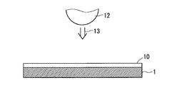
- ultraviolet rays 13 are used on the entire main surface of the metal oxide film 10 formed on the substrate 1 using an ultraviolet lamp 12 or the like. Irradiate. Irradiation with the ultraviolet rays 13 can reduce the resistance (resistivity) of the metal oxide film 10.
- the wavelength of the ultraviolet ray 13 to be irradiated is determined according to the film thickness of the metal oxide film 10 during the ultraviolet ray irradiation treatment. Then, the entire main surface of the metal oxide film 10 is irradiated with ultraviolet rays 13 having the determined wavelength.
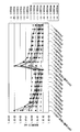
- FIG. 3 and 4 are experimental data showing the relationship between the resistivity of the metal oxide film and the ultraviolet irradiation for each of a plurality of film thicknesses of the metal oxide film (zinc oxide film).
- FIG. 4 is obtained by selecting data on the thickness of a metal oxide film having an arbitrary thickness from the experimental data shown in FIG.
- the first heat treatment is performed for 20 minutes on the metal oxide film formed under non-vacuum, and the metal oxide film after the first heat treatment is applied to the metal oxide film.
- an ultraviolet ray having a central wavelength of 254 nm is irradiated for 60 minutes, and thereafter, the metallic oxide film is irradiated with an ultraviolet ray having a central wavelength of 365 nm for 60 minutes, and then the metallic oxide film is irradiated with 2
- the second heat treatment is performed for 20 minutes, and the metal oxide film after the second heat treatment is irradiated with ultraviolet light having a center wavelength of 365 nm for 60 minutes, and then the center wavelength is applied to the metal oxide film.
- FIG. 3 relates to data on metal oxide films having film thicknesses (259 nm, 303 nm, 334 nm, 374 nm, 570 nm, 650 nm, 1344 nm, 1462 nm, 1863 nm, 2647 nm, 3033 nm, 3041 nm, 3805 nm, 3991 nm, 8109 nm).
- FIG. 4 relates to data on metal oxide films having film thicknesses (334 nm, 570 nm, 650 nm, 1344 nm, and 3033 nm).
- the first and second heat treatments are heating at a temperature (for example, 300 ° C. or less) that does not cause a change in crystallinity of the metal oxide film (such as filling of oxygen vacancies in ZnO).
- a temperature for example, 300 ° C. or less
- the metal oxide film was heated to 200 ° C.
- the metal oxide film (ZnO: zinc oxide film) formed in the experiment was produced (deposited) by the above process using the apparatus shown in FIG.
- the heating temperature of the substrate 1 during the film formation is 200 ° C.
- the supply amount of the solution 5 containing zinc (Zn) is 0.7 to 0.8 mmol / min
- the oxidation source 6 is water.
- the feed rate of is from 44 to 89 mmol / min.
- concentration of zinc in the solution 5 containing zinc is 0.35 mol / liter.
- the resistivity of the metal oxide film formed under non-vacuum is higher than that of the metal oxide film formed under vacuum. As shown in the experimental data shown in FIGS. 3 and 4, it is understood that the resistivity of the metal oxide film is reduced by irradiating the metal oxide film formed under non-vacuum with ultraviolet rays. It was.
- the metal oxide film formed under non-vacuum is irradiated with ultraviolet rays and subjected to a heating process
- the metal oxide film becomes high resistance. It is effective to irradiate the oxide film with ultraviolet rays from the viewpoint of reducing the resistance of the metal oxide film.
- the heating process (heating process) and the ultraviolet irradiation process are repeatedly performed on the metal oxide film, the resistance increased by the heating process can be reduced after the ultraviolet irradiation process.
- first ultraviolet light the slope indicating the decrease in resistivity of the metal oxide film when irradiated with ultraviolet light having a center wavelength of 254 nm (referred to as first ultraviolet light) after the first heat treatment, and the second heating. Attention is focused on the slope indicating the decrease in resistivity of the metal oxide film when irradiated with ultraviolet light having a center wavelength of 365 nm after processing (referred to as second ultraviolet light).
- the first ultraviolet irradiation can significantly reduce the resistivity of the metal oxide film in a shorter time than the second ultraviolet irradiation. it can.
- the second ultraviolet irradiation significantly reduces the resistivity of the metal oxide film in a shorter time than the first ultraviolet irradiation. be able to.
- ⁇ is an absorption coefficient
- ⁇ 4 ⁇ k / ⁇ (k: extinction coefficient, ⁇ : wavelength). That is, the penetration depth of ultraviolet rays into the metal oxide film is proportional to the wavelength of the ultraviolet rays (the larger the ultraviolet wavelength, the deeper the ultraviolet rays can penetrate into the metal oxide film).
- the entire thickness direction of the thick metal oxide film is not irradiated with ultraviolet light, resulting in a low resistance of the metal oxide film.
- the efficiency of conversion is reduced. Therefore, from the viewpoint of efficient resistance reduction, it is desirable to proportionally increase the wavelength of the determined ultraviolet light as the thickness of the metal oxide film increases.
- the metal oxide film (zinc oxide film) does not absorb the ultraviolet rays. Therefore, for the zinc oxide film, it is necessary that the wavelength of the irradiated ultraviolet light be 380 nm or less.
- a light source for irradiating ultraviolet light having a wavelength of 254 nm and a light source for irradiating ultraviolet light having a wavelength of 365 nm are available at a relatively low cost. Therefore, it is very useful to find out which wavelength of 254 nm and 365 nm is selected according to the thickness of the metal oxide film in order to reduce the resistance more efficiently.
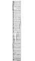
- FIG. 5 is a table showing which wavelength of 254 nm and 365 nm is useful for the ultraviolet rays irradiated in accordance with the thickness of the metal oxide film.
- FIG. 5 is created using the data shown in FIG.
- the uppermost column in FIG. 5 is the thickness of the metal oxide film (259 nm, 303 nm, 334 nm, 374 nm, 570 nm, 650 nm, 1344 nm, 1462 nm, 1863 nm, 2647 nm, 3033 nm, 3041 nm, 3805 nm, 3991 nm, 8109 nm). Further, the leftmost column in FIG. 5 shows the ultraviolet irradiation time (1 minute, 5 minutes, 10 minutes, 30 minutes, 60 minutes).
- each column of FIG. 5 the numerical values in each column of FIG. 5 are (the resistivity of the metal oxide film after the irradiation time has elapsed when irradiated with ultraviolet light having a central wavelength of 254 nm) / (when irradiated with ultraviolet light having a central wavelength of 365 nm).
- the value of the second row of the third column is “after the irradiation when the metal oxide film having a film thickness of 303 nm is irradiated with ultraviolet light having a central wavelength of 254 nm for 1 minute. Is divided by "the resistivity of the metal oxide film after irradiation when the metal oxide film having a film thickness of 303 nm is irradiated with ultraviolet light having a central wavelength of 365 nm for one minute”. The value is “0.8”.
- the value of the fifth row in the seventh column is “when a metal oxide film having a film thickness of 650 nm is irradiated with ultraviolet light having a central wavelength of 254 nm for 30 minutes, after the irradiation. Is divided by "the resistivity of the metal oxide film after irradiation when the metal oxide film having a thickness of 650 nm is irradiated with ultraviolet light having a central wavelength of 365 nm for 30 minutes”. The value is “2.6”.
- resistivity comparison ratio the resistivity of the metal oxide film after the irradiation time has elapsed when irradiated with ultraviolet light having a central wavelength of 254 nm
- the metal oxide film is more efficiently irradiated with ultraviolet rays having a central wavelength of 254 nm than when irradiated with ultraviolet rays having a central wavelength of 365 nm. This means that low resistance can be realized.
- the resistivity comparison ratio is greater than “1”
- the metal oxide is more efficiently irradiated with ultraviolet rays having a central wavelength of 365 nm than when irradiated with ultraviolet rays having a central wavelength of 254 nm. This means that the resistance of the film can be reduced.
- the irradiation with ultraviolet light having a central wavelength of 254 nm is more effective than the irradiation with ultraviolet light having a central wavelength of 365 nm. It can be seen that the resistance of the metal oxide film can be efficiently reduced.
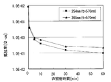
- FIG. 6 shows this more clearly.
- a metal oxide film having a film thickness of 570 nm is irradiated with ultraviolet light having a central wavelength of 254 nm and resistivity.
- the change in resistivity and the ultraviolet irradiation with a central wavelength of 365 nm is shown.
- the irradiation with ultraviolet light having a central wavelength of 254 nm is more efficient than the irradiation with ultraviolet light having a central wavelength of 365 nm.
- the resistance of the metal oxide film can be reduced.
- FIG. 7 shows this more clearly.
- a metal oxide film having a film thickness of 650 nm is irradiated with ultraviolet light having a central wavelength of 254 nm and resistivity.
- the change in resistivity and the ultraviolet irradiation with a central wavelength of 365 nm is shown.
- the irradiation with ultraviolet light having a central wavelength of 365 nm is more efficient than the irradiation with ultraviolet light having a central wavelength of 254 nm.
- the resistance of the metal oxide film can be reduced.
- the resistivity comparison ratio is linear between the film thicknesses 570 nm and 650 nm.
- the average value was calculated using the rise. As a result, it was found that the resistivity comparison ratio becomes “1” when the thickness of the metal oxide film is about 590 nm.
- the inventors found that the efficiency when irradiated with ultraviolet light having a central wavelength of 254 nm was higher than that when irradiated with ultraviolet light having a central wavelength of 365 nm. It has been found that low resistance of the metal oxide film can be realized well.
- the inventors have found that in the case of a metal oxide film having a film thickness greater than 590 nm, the efficiency when irradiated with ultraviolet light having a central wavelength of 365 nm is higher than that when irradiated with ultraviolet light having a central wavelength of 254 nm. It has been found that low resistance of the metal oxide film can be realized well.
- the metal oxide film has the same efficiency when irradiated with ultraviolet light having a central wavelength of 254 nm and when irradiated with ultraviolet light having a central wavelength of 365 nm. It is considered that the resistance can be lowered.
- the thickness of the metal oxide film is smaller than 590 nm, a wavelength including at least 254 nm is selected, and if the thickness of the metal oxide film is larger than 590 nm, It is desirable to select the wavelength including at least 365 nm from the viewpoint of reducing the cost of ultraviolet irradiation and improving the resistance reduction efficiency.
- the resistance of the metal oxide film can be lowered by irradiating the metal oxide film after film formation and the metal oxide film after heat treatment with ultraviolet light, and the resistance can be reduced efficiently
- select and determine the wavelength of the ultraviolet rays to be irradiated according to the thickness of the metal oxide film when the metal oxide film contains a dopant and when the metal oxide film contains no dopant. Both have been confirmed.
- the above explanations are applicable regardless of the type of dopant such as boron or indium even when the metal oxide film contains a dopant.
- the solution 5 containing zinc is misted, and the mist-formed solution 5 is sprayed on the substrate 1 in a non-vacuum state.
- 1 is formed with a metal oxide film 10 (FIG. 1).
- the metal oxide film 10 is irradiated with ultraviolet rays 13 (FIG. 2).
- the resistance of the metal oxide film is reduced by subsequent ultraviolet irradiation.
- the resistance of the metal oxide film formed under non-vacuum can be reduced to the same extent as the resistance of the metal oxide film formed under vacuum).
- the metal oxide film manufacturing method according to the present embodiment it is not necessary to employ a vacuum system or the like as a manufacturing (film forming) apparatus (that is, a film forming process under non-vacuum). Cost can be reduced and convenience is improved.
- the wavelength of ultraviolet rays to be irradiated is determined according to the thickness of the metal oxide film. For example, as the thickness of the metal oxide film increases, an ultraviolet wavelength having a larger value is selected.
- the metal oxide film can be irradiated with ultraviolet light having a wavelength that can reduce the resistance and increase the efficiency (reducing the resistivity in a short time).
- the thickness of the metal oxide film when the thickness of the metal oxide film is smaller than 590 nm, a wavelength including at least 254 nm is selected and determined, and the thickness of the metal oxide film is greater than 590 nm. If it is larger, a wavelength including at least 365 nm may be selected and determined.
- An ultraviolet light source having a wavelength of 254 nm and an ultraviolet light source having a wavelength of 365 nm are inexpensive. Then, ultraviolet rays capable of reducing resistance with high efficiency are selected according to the thickness of the metal oxide film. Therefore, in the method for manufacturing a metal oxide film according to the present invention in which the selection and determination of the wavelength is performed, it is possible to achieve low resistance and high efficiency of the metal oxide film and reduction in manufacturing cost.
- ultraviolet irradiation may be performed after the metal oxide film is formed to reduce the resistance of the metal oxide film.
- the metal oxide film having a high resistance may be irradiated with ultraviolet rays to reduce the resistance of the metal oxide film having a high resistance.
- the ultraviolet irradiation treatment may be performed every time after each heat treatment, and after the last heat treatment after performing the plurality of heat treatments.
- the ultraviolet treatment may be performed once. It should be noted that the selection and determination of the wavelength at the time of ultraviolet irradiation is preferably performed from the viewpoint of high efficiency and low resistance as described above.
- the metal oxide film After the metal oxide film is formed, it may be required in the manufacturing process that the metal oxide film is subjected to at least one heat treatment. Even in that case, the resistance of the metal oxide film having a high resistance can be reduced by performing the ultraviolet irradiation after the heat treatment. In addition, by selecting and determining the wavelength at the time of the ultraviolet irradiation to a predetermined value, and irradiating the metal oxide film having a high resistance with the ultraviolet light having the selected and determined wavelength, the metal oxide film is made high. Low resistance to efficiency.
Landscapes
- Chemical & Material Sciences (AREA)
- Engineering & Computer Science (AREA)
- Organic Chemistry (AREA)
- Materials Engineering (AREA)
- Metallurgy (AREA)
- Mechanical Engineering (AREA)
- General Chemical & Material Sciences (AREA)
- Chemical Kinetics & Catalysis (AREA)
- Physics & Mathematics (AREA)
- Thermal Sciences (AREA)
- Inorganic Chemistry (AREA)
- Health & Medical Sciences (AREA)
- Toxicology (AREA)
- Manufacturing & Machinery (AREA)
- Ceramic Engineering (AREA)
- General Health & Medical Sciences (AREA)
- Inorganic Compounds Of Heavy Metals (AREA)
- Manufacturing Of Electric Cables (AREA)
Description
本発明に係る金属酸化膜の製造方法では、非真空(大気圧)下での成膜処理を行う。具体的に、本発明に係る金属酸化膜の製造方法を、図1に示した製造装置(成膜装置)を用いて説明する。
2 加熱器
3A,3B 容器
4A,4B 霧化器
5 溶液
6 酸化源
8 ノズル
10 金属酸化膜(透明導電膜、亜鉛酸化膜)
12 紫外線ランプ
13 紫外線
L1,L2 経路
Claims (6)
- (A)亜鉛を含む溶液(5)をミスト化し、当該ミスト化した溶液を非真空下において基板(1)に対して噴霧することにより、前記基板に金属酸化膜(10)を成膜する工程と、
(B)前記金属酸化膜に対して、紫外線(13)を照射することにより、前記金属酸化膜の抵抗を下げる工程とを、備えており、
前記工程(B)は、
(B-1)前記金属酸化膜の膜厚に応じて、照射する前記紫外線の波長を決定する工程と、
(B-2)前記工程(B-1)で決定した波長を有する前記紫外線を、前記金属酸化膜に照射する工程とを、有する、
ことを特徴とする金属酸化膜の製造方法。 - 前記工程(B-1)は、
前記金属酸化膜の膜厚が厚くなるに従い、前記紫外線の前記波長として大きい値のものを選択する、
ことを特徴とする請求項1に記載の金属酸化膜の製造方法。 - 前記工程(B-1)は、
前記金属酸化膜の膜厚が590nmより小さい場合には、少なくとも254nmを含む前記波長を選択する、
ことを特徴とする請求項1に記載の金属酸化膜の製造方法。 - 前記工程(B-1)は、
前記金属酸化膜の膜厚が590nmより大きい場合には、少なくとも365nmを含む前記波長を選択する、
ことを特徴とする請求項1に記載の金属酸化膜の製造方法。 - (C)前記金属酸化膜に対して加熱を行う工程を、さらに備えており、
前記工程(B)は、
前記工程(C)の後に実施する、
ことを特徴とする請求項1に記載の金属酸化膜の製造方法。 - 請求項1乃至請求項5の何れかに記載の金属酸化膜の製造方法により作製された、ことを特徴とする金属酸化膜。
Priority Applications (10)
| Application Number | Priority Date | Filing Date | Title |
|---|---|---|---|
| KR1020147019128A KR20140101854A (ko) | 2012-02-08 | 2012-10-24 | 금속산화막의 제조 방법 및 금속산화막 |
| KR1020187014499A KR20180058856A (ko) | 2012-02-08 | 2012-10-24 | 금속산화막의 제조 방법 및 금속산화막 |
| KR1020167021468A KR20160098523A (ko) | 2012-02-08 | 2012-10-24 | 금속산화막의 제조 방법 및 금속산화막 |
| KR1020167014246A KR20160075761A (ko) | 2012-02-08 | 2012-10-24 | 금속산화막의 제조 방법 및 금속산화막 |
| HK14111745.9A HK1198183B (en) | 2012-02-08 | 2012-10-24 | Method for producing metal oxide film and metal oxide film |
| US14/368,954 US20150010464A1 (en) | 2012-02-08 | 2012-10-24 | Method for producing metal oxide film and metal oxide film |
| JP2013557364A JP5651790B2 (ja) | 2012-02-08 | 2012-10-24 | 金属酸化膜の製造方法 |
| DE112012005843.7T DE112012005843B4 (de) | 2012-02-08 | 2012-10-24 | Verfahren zur Herstellung einer Metalloxidschicht |
| CN201280069377.1A CN104105817B (zh) | 2012-02-08 | 2012-10-24 | 金属氧化膜的制造方法和金属氧化膜 |
| TW102103678A TWI552204B (zh) | 2012-02-08 | 2013-01-31 | 金屬氧化膜之製造方法及金屬氧化膜 |
Applications Claiming Priority (2)
| Application Number | Priority Date | Filing Date | Title |
|---|---|---|---|
| JPPCT/JP2012/052835 | 2012-02-08 | ||
| JP2012052835 | 2012-02-08 |
Publications (1)
| Publication Number | Publication Date |
|---|---|
| WO2013118353A1 true WO2013118353A1 (ja) | 2013-08-15 |
Family
ID=48947140
Family Applications (1)
| Application Number | Title | Priority Date | Filing Date |
|---|---|---|---|
| PCT/JP2012/077416 Ceased WO2013118353A1 (ja) | 2012-02-08 | 2012-10-24 | 金属酸化膜の製造方法および金属酸化膜 |
Country Status (6)
| Country | Link |
|---|---|
| US (1) | US20150010464A1 (ja) |
| KR (4) | KR20160098523A (ja) |
| CN (1) | CN104105817B (ja) |
| DE (1) | DE112012005843B4 (ja) |
| TW (1) | TWI552204B (ja) |
| WO (1) | WO2013118353A1 (ja) |
Cited By (1)
| Publication number | Priority date | Publication date | Assignee | Title |
|---|---|---|---|---|
| US11628468B2 (en) | 2018-08-01 | 2023-04-18 | Nikon Corporation | Mist generator, mist film formation method and mist film formation apparatus |
Families Citing this family (2)
| Publication number | Priority date | Publication date | Assignee | Title |
|---|---|---|---|---|
| DE112015006632B4 (de) | 2015-06-18 | 2023-09-21 | Kochi Prefectural Public University Corporation | Verfahren zur Bildung eines Metalloxidfilms |
| US10622775B2 (en) | 2016-07-04 | 2020-04-14 | Mando Corporation | Power supply apparatus for field winding motor and field winding motor including the same |
Citations (2)
| Publication number | Priority date | Publication date | Assignee | Title |
|---|---|---|---|---|
| JP2005029408A (ja) * | 2003-07-09 | 2005-02-03 | Nippon Shokubai Co Ltd | 金属酸化物膜の形成方法 |
| JP2011170979A (ja) * | 2010-02-16 | 2011-09-01 | Univ Of Miyazaki | 酸化亜鉛薄膜製造方法、およびこの方法で製造した帯電防止薄膜、紫外線カット薄膜、透明電極薄膜 |
Family Cites Families (7)
| Publication number | Priority date | Publication date | Assignee | Title |
|---|---|---|---|---|
| JPH0945140A (ja) | 1995-07-28 | 1997-02-14 | Sumitomo Metal Mining Co Ltd | 酸化亜鉛系透明導電性膜 |
| JP4110752B2 (ja) * | 2001-06-28 | 2008-07-02 | 富士ゼロックス株式会社 | 基材上に設けた透明導電膜を低抵抗化する方法。 |
| US7253125B1 (en) * | 2004-04-16 | 2007-08-07 | Novellus Systems, Inc. | Method to improve mechanical strength of low-k dielectric film using modulated UV exposure |
| JP4705340B2 (ja) * | 2004-06-14 | 2011-06-22 | 日本曹達株式会社 | 酸化インジウム膜の製造方法 |
| DE112008004011T5 (de) * | 2008-09-24 | 2011-07-14 | Toshiba Mitsubishi-Electric Industrial Systems Corporation | Verfahren zur Bildung von Zinkoxidfilm (ZnO) oder Magnesiumzinkoxidfilm (ZnMgO) und Anlage zur Bildung von Zinkoxidfilm oder Magnesiumzinkoxidfilm |
| JP5271355B2 (ja) * | 2008-09-24 | 2013-08-21 | 東芝三菱電機産業システム株式会社 | 金属酸化膜の成膜方法および金属酸化膜の成膜装置 |
| JP5411681B2 (ja) | 2009-12-09 | 2014-02-12 | スタンレー電気株式会社 | 酸化亜鉛系半導体の成長方法及び半導体発光素子の製造方法 |
-
2012
- 2012-10-24 KR KR1020167021468A patent/KR20160098523A/ko not_active Ceased
- 2012-10-24 DE DE112012005843.7T patent/DE112012005843B4/de active Active
- 2012-10-24 CN CN201280069377.1A patent/CN104105817B/zh active Active
- 2012-10-24 KR KR1020187014499A patent/KR20180058856A/ko not_active Ceased
- 2012-10-24 WO PCT/JP2012/077416 patent/WO2013118353A1/ja not_active Ceased
- 2012-10-24 US US14/368,954 patent/US20150010464A1/en not_active Abandoned
- 2012-10-24 KR KR1020147019128A patent/KR20140101854A/ko not_active Ceased
- 2012-10-24 KR KR1020167014246A patent/KR20160075761A/ko not_active Abandoned
-
2013
- 2013-01-31 TW TW102103678A patent/TWI552204B/zh active
Patent Citations (2)
| Publication number | Priority date | Publication date | Assignee | Title |
|---|---|---|---|---|
| JP2005029408A (ja) * | 2003-07-09 | 2005-02-03 | Nippon Shokubai Co Ltd | 金属酸化物膜の形成方法 |
| JP2011170979A (ja) * | 2010-02-16 | 2011-09-01 | Univ Of Miyazaki | 酸化亜鉛薄膜製造方法、およびこの方法で製造した帯電防止薄膜、紫外線カット薄膜、透明電極薄膜 |
Cited By (1)
| Publication number | Priority date | Publication date | Assignee | Title |
|---|---|---|---|---|
| US11628468B2 (en) | 2018-08-01 | 2023-04-18 | Nikon Corporation | Mist generator, mist film formation method and mist film formation apparatus |
Also Published As
| Publication number | Publication date |
|---|---|
| US20150010464A1 (en) | 2015-01-08 |
| KR20140101854A (ko) | 2014-08-20 |
| TW201340179A (zh) | 2013-10-01 |
| KR20160075761A (ko) | 2016-06-29 |
| HK1198183A1 (zh) | 2015-03-13 |
| DE112012005843B4 (de) | 2025-04-24 |
| CN104105817A (zh) | 2014-10-15 |
| TWI552204B (zh) | 2016-10-01 |
| DE112012005843T8 (de) | 2015-02-05 |
| KR20160098523A (ko) | 2016-08-18 |
| KR20180058856A (ko) | 2018-06-01 |
| CN104105817B (zh) | 2016-02-24 |
| DE112012005843T5 (de) | 2014-10-30 |
Similar Documents
| Publication | Publication Date | Title |
|---|---|---|
| JP2006165531A5 (ja) | ||
| JP5645191B2 (ja) | 金属酸化膜の成膜方法および金属酸化膜 | |
| JP5652768B2 (ja) | 金属酸化膜の成膜方法、金属酸化膜および金属酸化膜の成膜装置 | |
| WO2013118353A1 (ja) | 金属酸化膜の製造方法および金属酸化膜 | |
| JP5651790B2 (ja) | 金属酸化膜の製造方法 | |
| EP2662864A1 (en) | Method for enhancing conductivity of transparent metal oxide. | |
| TWI593130B (zh) | 太陽能電池的製造方法 | |
| JP5956559B2 (ja) | 金属酸化膜の製造方法 | |
| HK1198183B (en) | Method for producing metal oxide film and metal oxide film | |
| KR20180118964A (ko) | 개선된 저온 공정을 이용한 산화물 박막 제조 장치 및 방법 | |
| JP6329533B2 (ja) | 成膜方法 | |
| JP6174251B2 (ja) | バッファ層の成膜方法 | |
| JP6486696B2 (ja) | 薄膜堆積方法及び薄膜堆積装置 | |
| JP2018168005A (ja) | 酸化金の分解と保存の制御方法 | |
| JP2010192294A (ja) | 透明導電膜の製造方法、透明導電膜およびデバイス | |
| US20110259369A1 (en) | Method for cleaning deposition chamber | |
| JP2008282738A (ja) | 酸化亜鉛透明導電膜付き支持基板の製造方法。 |
Legal Events
| Date | Code | Title | Description |
|---|---|---|---|
| WWE | Wipo information: entry into national phase |
Ref document number: 201280069377.1 Country of ref document: CN |
|
| 121 | Ep: the epo has been informed by wipo that ep was designated in this application |
Ref document number: 12867990 Country of ref document: EP Kind code of ref document: A1 |
|
| ENP | Entry into the national phase |
Ref document number: 2013557364 Country of ref document: JP Kind code of ref document: A |
|
| ENP | Entry into the national phase |
Ref document number: 20147019128 Country of ref document: KR Kind code of ref document: A |
|
| WWE | Wipo information: entry into national phase |
Ref document number: 1120120058437 Country of ref document: DE Ref document number: 112012005843 Country of ref document: DE |
|
| 122 | Ep: pct application non-entry in european phase |
Ref document number: 12867990 Country of ref document: EP Kind code of ref document: A1 |
|
| WWG | Wipo information: grant in national office |
Ref document number: 112012005843 Country of ref document: DE |