WO2013111434A1 - 接合体および半導体モジュール - Google Patents
接合体および半導体モジュール Download PDFInfo
- Publication number
- WO2013111434A1 WO2013111434A1 PCT/JP2012/080121 JP2012080121W WO2013111434A1 WO 2013111434 A1 WO2013111434 A1 WO 2013111434A1 JP 2012080121 W JP2012080121 W JP 2012080121W WO 2013111434 A1 WO2013111434 A1 WO 2013111434A1
- Authority
- WO
- WIPO (PCT)
- Prior art keywords
- adhesive member
- glass
- mass
- metal
- adhesive
- Prior art date
- Legal status (The legal status is an assumption and is not a legal conclusion. Google has not performed a legal analysis and makes no representation as to the accuracy of the status listed.)
- Ceased
Links
Images

Classifications
-
- H—ELECTRICITY
- H10—SEMICONDUCTOR DEVICES; ELECTRIC SOLID-STATE DEVICES NOT OTHERWISE PROVIDED FOR
- H10W—GENERIC PACKAGES, INTERCONNECTIONS, CONNECTORS OR OTHER CONSTRUCTIONAL DETAILS OF DEVICES COVERED BY CLASS H10
- H10W40/00—Arrangements for thermal protection or thermal control
- H10W40/20—Arrangements for cooling
- H10W40/25—Arrangements for cooling characterised by their materials
- H10W40/258—Metallic materials
-
- B—PERFORMING OPERATIONS; TRANSPORTING
- B23—MACHINE TOOLS; METAL-WORKING NOT OTHERWISE PROVIDED FOR
- B23K—SOLDERING OR UNSOLDERING; WELDING; CLADDING OR PLATING BY SOLDERING OR WELDING; CUTTING BY APPLYING HEAT LOCALLY, e.g. FLAME CUTTING; WORKING BY LASER BEAM
- B23K35/00—Rods, electrodes, materials, or media, for use in soldering, welding, or cutting
- B23K35/22—Rods, electrodes, materials, or media, for use in soldering, welding, or cutting characterised by the composition or nature of the material
- B23K35/24—Selection of soldering or welding materials proper
- B23K35/26—Selection of soldering or welding materials proper with the principal constituent melting at less than 400°C
-
- C—CHEMISTRY; METALLURGY
- C04—CEMENTS; CONCRETE; ARTIFICIAL STONE; CERAMICS; REFRACTORIES
- C04B—LIME, MAGNESIA; SLAG; CEMENTS; COMPOSITIONS THEREOF, e.g. MORTARS, CONCRETE OR LIKE BUILDING MATERIALS; ARTIFICIAL STONE; CERAMICS; REFRACTORIES; TREATMENT OF NATURAL STONE
- C04B37/00—Joining burned ceramic articles with other burned ceramic articles or other articles by heating
- C04B37/02—Joining burned ceramic articles with other burned ceramic articles or other articles by heating with metallic articles
- C04B37/023—Joining burned ceramic articles with other burned ceramic articles or other articles by heating with metallic articles characterised by the interlayer used
- C04B37/025—Joining burned ceramic articles with other burned ceramic articles or other articles by heating with metallic articles characterised by the interlayer used consisting of glass or ceramic material
-
- C—CHEMISTRY; METALLURGY
- C04—CEMENTS; CONCRETE; ARTIFICIAL STONE; CERAMICS; REFRACTORIES
- C04B—LIME, MAGNESIA; SLAG; CEMENTS; COMPOSITIONS THEREOF, e.g. MORTARS, CONCRETE OR LIKE BUILDING MATERIALS; ARTIFICIAL STONE; CERAMICS; REFRACTORIES; TREATMENT OF NATURAL STONE
- C04B37/00—Joining burned ceramic articles with other burned ceramic articles or other articles by heating
- C04B37/02—Joining burned ceramic articles with other burned ceramic articles or other articles by heating with metallic articles
- C04B37/023—Joining burned ceramic articles with other burned ceramic articles or other articles by heating with metallic articles characterised by the interlayer used
- C04B37/026—Joining burned ceramic articles with other burned ceramic articles or other articles by heating with metallic articles characterised by the interlayer used consisting of metals or metal salts
-
- C—CHEMISTRY; METALLURGY
- C22—METALLURGY; FERROUS OR NON-FERROUS ALLOYS; TREATMENT OF ALLOYS OR NON-FERROUS METALS
- C22C—ALLOYS
- C22C13/00—Alloys based on tin
-
- C—CHEMISTRY; METALLURGY
- C22—METALLURGY; FERROUS OR NON-FERROUS ALLOYS; TREATMENT OF ALLOYS OR NON-FERROUS METALS
- C22C—ALLOYS
- C22C5/00—Alloys based on noble metals
- C22C5/06—Alloys based on silver
-
- H—ELECTRICITY
- H10—SEMICONDUCTOR DEVICES; ELECTRIC SOLID-STATE DEVICES NOT OTHERWISE PROVIDED FOR
- H10H—INORGANIC LIGHT-EMITTING SEMICONDUCTOR DEVICES HAVING POTENTIAL BARRIERS
- H10H20/00—Individual inorganic light-emitting semiconductor devices having potential barriers, e.g. light-emitting diodes [LED]
- H10H20/80—Constructional details
- H10H20/85—Packages
- H10H20/857—Interconnections, e.g. lead-frames, bond wires or solder balls
-
- H—ELECTRICITY
- H10—SEMICONDUCTOR DEVICES; ELECTRIC SOLID-STATE DEVICES NOT OTHERWISE PROVIDED FOR
- H10H—INORGANIC LIGHT-EMITTING SEMICONDUCTOR DEVICES HAVING POTENTIAL BARRIERS
- H10H20/00—Individual inorganic light-emitting semiconductor devices having potential barriers, e.g. light-emitting diodes [LED]
- H10H20/80—Constructional details
- H10H20/85—Packages
- H10H20/858—Means for heat extraction or cooling
- H10H20/8581—Means for heat extraction or cooling characterised by their material
-
- H—ELECTRICITY
- H10—SEMICONDUCTOR DEVICES; ELECTRIC SOLID-STATE DEVICES NOT OTHERWISE PROVIDED FOR
- H10W—GENERIC PACKAGES, INTERCONNECTIONS, CONNECTORS OR OTHER CONSTRUCTIONAL DETAILS OF DEVICES COVERED BY CLASS H10
- H10W40/00—Arrangements for thermal protection or thermal control
- H10W40/20—Arrangements for cooling
- H10W40/25—Arrangements for cooling characterised by their materials
- H10W40/255—Arrangements for cooling characterised by their materials having a laminate or multilayered structure, e.g. direct bond copper [DBC] ceramic substrates
-
- H—ELECTRICITY
- H10—SEMICONDUCTOR DEVICES; ELECTRIC SOLID-STATE DEVICES NOT OTHERWISE PROVIDED FOR
- H10W—GENERIC PACKAGES, INTERCONNECTIONS, CONNECTORS OR OTHER CONSTRUCTIONAL DETAILS OF DEVICES COVERED BY CLASS H10
- H10W72/00—Interconnections or connectors in packages
- H10W72/071—Connecting or disconnecting
-
- H—ELECTRICITY
- H10—SEMICONDUCTOR DEVICES; ELECTRIC SOLID-STATE DEVICES NOT OTHERWISE PROVIDED FOR
- H10W—GENERIC PACKAGES, INTERCONNECTIONS, CONNECTORS OR OTHER CONSTRUCTIONAL DETAILS OF DEVICES COVERED BY CLASS H10
- H10W72/00—Interconnections or connectors in packages
- H10W72/60—Strap connectors, e.g. thick copper clips for grounding of power devices
-
- C—CHEMISTRY; METALLURGY
- C04—CEMENTS; CONCRETE; ARTIFICIAL STONE; CERAMICS; REFRACTORIES
- C04B—LIME, MAGNESIA; SLAG; CEMENTS; COMPOSITIONS THEREOF, e.g. MORTARS, CONCRETE OR LIKE BUILDING MATERIALS; ARTIFICIAL STONE; CERAMICS; REFRACTORIES; TREATMENT OF NATURAL STONE
- C04B2235/00—Aspects relating to ceramic starting mixtures or sintered ceramic products
- C04B2235/70—Aspects relating to sintered or melt-casted ceramic products
- C04B2235/96—Properties of ceramic products, e.g. mechanical properties such as strength, toughness, wear resistance
- C04B2235/9607—Thermal properties, e.g. thermal expansion coefficient
-
- C—CHEMISTRY; METALLURGY
- C04—CEMENTS; CONCRETE; ARTIFICIAL STONE; CERAMICS; REFRACTORIES
- C04B—LIME, MAGNESIA; SLAG; CEMENTS; COMPOSITIONS THEREOF, e.g. MORTARS, CONCRETE OR LIKE BUILDING MATERIALS; ARTIFICIAL STONE; CERAMICS; REFRACTORIES; TREATMENT OF NATURAL STONE
- C04B2237/00—Aspects relating to ceramic laminates or to joining of ceramic articles with other articles by heating
- C04B2237/02—Aspects relating to interlayers, e.g. used to join ceramic articles with other articles by heating
- C04B2237/10—Glass interlayers, e.g. frit or flux
-
- C—CHEMISTRY; METALLURGY
- C04—CEMENTS; CONCRETE; ARTIFICIAL STONE; CERAMICS; REFRACTORIES
- C04B—LIME, MAGNESIA; SLAG; CEMENTS; COMPOSITIONS THEREOF, e.g. MORTARS, CONCRETE OR LIKE BUILDING MATERIALS; ARTIFICIAL STONE; CERAMICS; REFRACTORIES; TREATMENT OF NATURAL STONE
- C04B2237/00—Aspects relating to ceramic laminates or to joining of ceramic articles with other articles by heating
- C04B2237/02—Aspects relating to interlayers, e.g. used to join ceramic articles with other articles by heating
- C04B2237/12—Metallic interlayers
- C04B2237/125—Metallic interlayers based on noble metals, e.g. silver
-
- C—CHEMISTRY; METALLURGY
- C04—CEMENTS; CONCRETE; ARTIFICIAL STONE; CERAMICS; REFRACTORIES
- C04B—LIME, MAGNESIA; SLAG; CEMENTS; COMPOSITIONS THEREOF, e.g. MORTARS, CONCRETE OR LIKE BUILDING MATERIALS; ARTIFICIAL STONE; CERAMICS; REFRACTORIES; TREATMENT OF NATURAL STONE
- C04B2237/00—Aspects relating to ceramic laminates or to joining of ceramic articles with other articles by heating
- C04B2237/30—Composition of layers of ceramic laminates or of ceramic or metallic articles to be joined by heating, e.g. Si substrates
- C04B2237/32—Ceramic
- C04B2237/36—Non-oxidic
- C04B2237/366—Aluminium nitride
-
- C—CHEMISTRY; METALLURGY
- C04—CEMENTS; CONCRETE; ARTIFICIAL STONE; CERAMICS; REFRACTORIES
- C04B—LIME, MAGNESIA; SLAG; CEMENTS; COMPOSITIONS THEREOF, e.g. MORTARS, CONCRETE OR LIKE BUILDING MATERIALS; ARTIFICIAL STONE; CERAMICS; REFRACTORIES; TREATMENT OF NATURAL STONE
- C04B2237/00—Aspects relating to ceramic laminates or to joining of ceramic articles with other articles by heating
- C04B2237/30—Composition of layers of ceramic laminates or of ceramic or metallic articles to be joined by heating, e.g. Si substrates
- C04B2237/32—Ceramic
- C04B2237/36—Non-oxidic
- C04B2237/368—Silicon nitride
-
- C—CHEMISTRY; METALLURGY
- C04—CEMENTS; CONCRETE; ARTIFICIAL STONE; CERAMICS; REFRACTORIES
- C04B—LIME, MAGNESIA; SLAG; CEMENTS; COMPOSITIONS THEREOF, e.g. MORTARS, CONCRETE OR LIKE BUILDING MATERIALS; ARTIFICIAL STONE; CERAMICS; REFRACTORIES; TREATMENT OF NATURAL STONE
- C04B2237/00—Aspects relating to ceramic laminates or to joining of ceramic articles with other articles by heating
- C04B2237/30—Composition of layers of ceramic laminates or of ceramic or metallic articles to be joined by heating, e.g. Si substrates
- C04B2237/40—Metallic
- C04B2237/408—Noble metals, e.g. palladium, platina or silver
-
- H—ELECTRICITY
- H10—SEMICONDUCTOR DEVICES; ELECTRIC SOLID-STATE DEVICES NOT OTHERWISE PROVIDED FOR
- H10W—GENERIC PACKAGES, INTERCONNECTIONS, CONNECTORS OR OTHER CONSTRUCTIONAL DETAILS OF DEVICES COVERED BY CLASS H10
- H10W40/00—Arrangements for thermal protection or thermal control
- H10W40/20—Arrangements for cooling
- H10W40/25—Arrangements for cooling characterised by their materials
- H10W40/259—Ceramics or glasses
-
- H—ELECTRICITY
- H10—SEMICONDUCTOR DEVICES; ELECTRIC SOLID-STATE DEVICES NOT OTHERWISE PROVIDED FOR
- H10W—GENERIC PACKAGES, INTERCONNECTIONS, CONNECTORS OR OTHER CONSTRUCTIONAL DETAILS OF DEVICES COVERED BY CLASS H10
- H10W72/00—Interconnections or connectors in packages
- H10W72/071—Connecting or disconnecting
- H10W72/076—Connecting or disconnecting of strap connectors
- H10W72/07631—Techniques
- H10W72/07637—Techniques using a polymer adhesive, e.g. an adhesive based on silicone or epoxy
-
- H—ELECTRICITY
- H10—SEMICONDUCTOR DEVICES; ELECTRIC SOLID-STATE DEVICES NOT OTHERWISE PROVIDED FOR
- H10W—GENERIC PACKAGES, INTERCONNECTIONS, CONNECTORS OR OTHER CONSTRUCTIONAL DETAILS OF DEVICES COVERED BY CLASS H10
- H10W72/00—Interconnections or connectors in packages
- H10W72/071—Connecting or disconnecting
- H10W72/076—Connecting or disconnecting of strap connectors
- H10W72/07651—Connecting or disconnecting of strap connectors characterised by changes in properties of the strap connectors during connecting
- H10W72/07653—Connecting or disconnecting of strap connectors characterised by changes in properties of the strap connectors during connecting changes in shapes
-
- H—ELECTRICITY
- H10—SEMICONDUCTOR DEVICES; ELECTRIC SOLID-STATE DEVICES NOT OTHERWISE PROVIDED FOR
- H10W—GENERIC PACKAGES, INTERCONNECTIONS, CONNECTORS OR OTHER CONSTRUCTIONAL DETAILS OF DEVICES COVERED BY CLASS H10
- H10W72/00—Interconnections or connectors in packages
- H10W72/50—Bond wires
- H10W72/531—Shapes of wire connectors
- H10W72/536—Shapes of wire connectors the connected ends being ball-shaped
-
- H—ELECTRICITY
- H10—SEMICONDUCTOR DEVICES; ELECTRIC SOLID-STATE DEVICES NOT OTHERWISE PROVIDED FOR
- H10W—GENERIC PACKAGES, INTERCONNECTIONS, CONNECTORS OR OTHER CONSTRUCTIONAL DETAILS OF DEVICES COVERED BY CLASS H10
- H10W72/00—Interconnections or connectors in packages
- H10W72/851—Dispositions of multiple connectors or interconnections
- H10W72/853—On the same surface
- H10W72/871—Bond wires and strap connectors
-
- H—ELECTRICITY
- H10—SEMICONDUCTOR DEVICES; ELECTRIC SOLID-STATE DEVICES NOT OTHERWISE PROVIDED FOR
- H10W—GENERIC PACKAGES, INTERCONNECTIONS, CONNECTORS OR OTHER CONSTRUCTIONAL DETAILS OF DEVICES COVERED BY CLASS H10
- H10W72/00—Interconnections or connectors in packages
- H10W72/851—Dispositions of multiple connectors or interconnections
- H10W72/874—On different surfaces
- H10W72/884—Die-attach connectors and bond wires
-
- H—ELECTRICITY
- H10—SEMICONDUCTOR DEVICES; ELECTRIC SOLID-STATE DEVICES NOT OTHERWISE PROVIDED FOR
- H10W—GENERIC PACKAGES, INTERCONNECTIONS, CONNECTORS OR OTHER CONSTRUCTIONAL DETAILS OF DEVICES COVERED BY CLASS H10
- H10W72/00—Interconnections or connectors in packages
- H10W72/851—Dispositions of multiple connectors or interconnections
- H10W72/874—On different surfaces
- H10W72/886—Die-attach connectors and strap connectors
-
- H—ELECTRICITY
- H10—SEMICONDUCTOR DEVICES; ELECTRIC SOLID-STATE DEVICES NOT OTHERWISE PROVIDED FOR
- H10W—GENERIC PACKAGES, INTERCONNECTIONS, CONNECTORS OR OTHER CONSTRUCTIONAL DETAILS OF DEVICES COVERED BY CLASS H10
- H10W74/00—Encapsulations, e.g. protective coatings
-
- H—ELECTRICITY
- H10—SEMICONDUCTOR DEVICES; ELECTRIC SOLID-STATE DEVICES NOT OTHERWISE PROVIDED FOR
- H10W—GENERIC PACKAGES, INTERCONNECTIONS, CONNECTORS OR OTHER CONSTRUCTIONAL DETAILS OF DEVICES COVERED BY CLASS H10
- H10W90/00—Package configurations
- H10W90/701—Package configurations characterised by the relative positions of pads or connectors relative to package parts
- H10W90/731—Package configurations characterised by the relative positions of pads or connectors relative to package parts of die-attach connectors
- H10W90/736—Package configurations characterised by the relative positions of pads or connectors relative to package parts of die-attach connectors between a chip and a stacked lead frame, conducting package substrate or heat sink
-
- H—ELECTRICITY
- H10—SEMICONDUCTOR DEVICES; ELECTRIC SOLID-STATE DEVICES NOT OTHERWISE PROVIDED FOR
- H10W—GENERIC PACKAGES, INTERCONNECTIONS, CONNECTORS OR OTHER CONSTRUCTIONAL DETAILS OF DEVICES COVERED BY CLASS H10
- H10W90/00—Package configurations
- H10W90/701—Package configurations characterised by the relative positions of pads or connectors relative to package parts
- H10W90/751—Package configurations characterised by the relative positions of pads or connectors relative to package parts of bond wires
- H10W90/754—Package configurations characterised by the relative positions of pads or connectors relative to package parts of bond wires between a chip and a stacked insulating package substrate, interposer or RDL
-
- H—ELECTRICITY
- H10—SEMICONDUCTOR DEVICES; ELECTRIC SOLID-STATE DEVICES NOT OTHERWISE PROVIDED FOR
- H10W—GENERIC PACKAGES, INTERCONNECTIONS, CONNECTORS OR OTHER CONSTRUCTIONAL DETAILS OF DEVICES COVERED BY CLASS H10
- H10W90/00—Package configurations
- H10W90/701—Package configurations characterised by the relative positions of pads or connectors relative to package parts
- H10W90/761—Package configurations characterised by the relative positions of pads or connectors relative to package parts of strap connectors
- H10W90/764—Package configurations characterised by the relative positions of pads or connectors relative to package parts of strap connectors between a chip and a stacked insulating package substrate, interposer or RDL
-
- Y—GENERAL TAGGING OF NEW TECHNOLOGICAL DEVELOPMENTS; GENERAL TAGGING OF CROSS-SECTIONAL TECHNOLOGIES SPANNING OVER SEVERAL SECTIONS OF THE IPC; TECHNICAL SUBJECTS COVERED BY FORMER USPC CROSS-REFERENCE ART COLLECTIONS [XRACs] AND DIGESTS
- Y10—TECHNICAL SUBJECTS COVERED BY FORMER USPC
- Y10T—TECHNICAL SUBJECTS COVERED BY FORMER US CLASSIFICATION
- Y10T428/00—Stock material or miscellaneous articles
- Y10T428/12—All metal or with adjacent metals
- Y10T428/12014—All metal or with adjacent metals having metal particles
Definitions
- the present invention relates to a joining member for joining metal, ceramic, and semiconductor, and a semiconductor module using the joining member.
- a semiconductor module is manufactured by bonding a ceramic substrate to a base metal, bonding a metal wiring to the ceramic substrate, and bonding an element such as a semiconductor chip to the metal wiring.
- the adhesive used for bonding is called a die bonding material.
- Solder bonding is the mainstream for element bonding of conventional power device packages.
- conductive paste or lead-free solder mixed with Ag powder and resin is used as an alternative material because of the need for lead-free soldering.
- semiconductor elements such as semiconductor chips tend to be highly integrated and miniaturized, and accordingly, the amount of heat generated per unit area tends to increase. Therefore, in a semiconductor module on which a semiconductor element is mounted, it is necessary to efficiently release the heat generated from the semiconductor element to the outside, and improvement of the thermal conductivity of the die bonding material is an issue.
- the ceramic substrate bonding is mainly performed by metallizing a ceramic substrate such as AlN or Si 3 N 4 and bonding the metallized layer and the semiconductor chip or the metallized layer and the base metal by lead-free solder.
- a method for forming a strong metallization layer relaxation of the difference in thermal expansion coefficient between the substrate and the semiconductor chip, improvement in heat dissipation of the substrate, and improvement in long-term reliability such as heat cycleability.
- Patent Document 1 describes a lead-free solder paste, and provides a lead-free solder paste containing Bi solder powder and Cu metal powder and having a thermal conductivity of 52 W / mK.
- the adhesion between the ceramic substrate and the metal wiring is lowered unless the ceramic substrate is previously metallized. Further, when the lead-free solder is used for joining the metal wiring and the semiconductor chip, the thermal conductivity is lowered.
- An object of the present invention is to improve the adhesiveness and thermal conductivity of a bonded body in which any one of metal, ceramic, and semiconductor is bonded.
- the present invention provides a bonded body obtained by bonding a first member made of metal, ceramic, or semiconductor and a second member, and an adhesive member provided on the surface of the first member.
- the second member is bonded via the glass, and the bonding member contains glass containing V 2 O 5 and metal particles.
- the ceramic substrate is bonded via a first adhesive member provided on the surface of the base metal, and is attached to the surface of the ceramic substrate.
- the metal wiring is bonded via a second adhesive member provided
- the semiconductor chip is bonded via a third adhesive member provided on the surface of the metal wiring, and the first adhesive member and the second adhesive member
- the third adhesive member contains glass containing V 2 O 5 and metal particles.
- adhesion and thermal conductivity can be improved.
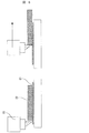
- FIG. 7 is a structural cross-sectional view of a semiconductor device. DTA curve of glass. Die shear strength test schematic diagram.
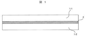
- the present invention relates to a joined body in which members (first member 1-1, second member 1-2) that are either metal, ceramic, or semiconductor are bonded.
- the joining member 2 to be joined contains glass and metal particles. It is assumed that vanadium oxide (V 2 O 5 ) is included as glass that can be bonded to any of metal, ceramic, and semiconductor. The thickness in the vertical direction of the figure may not be uniform at any position in the plane of the member. Further, the adhesive member 2 may not be bonded to the entire surface to which both members are bonded, and conversely may protrude from both members. In short, the adhesive member 2 may be formed in a layered manner between the first member 1-1 and the second member 1-2 and may be in close contact with each other.
- the joined body of the present invention when the joined body of the present invention is in an operating state in which a temperature difference is generated between the first member 1-1 and the second member 1-2 when energized, not only the two members are bonded together, Heat can move through the adhesive member 2 from the high temperature side member to the low temperature side member among the members. Therefore, for example, when the first member 1-1 is a heat generator and the second member 1-2 is a heat radiator, heat is released from the first member 1-1 to the second member 1-2 via the adhesive member 2. be able to.
- the joining member 2 is presupposed to be supplied and used as a paste. After the paste is applied and dried, calcination is performed to remove organic components, and then a joined body is obtained through a main firing step for joining the members. Therefore, it is desirable that the glass has less crystallinity than amorphous, and the degree of crystallinity is desirably 30% or less in order to reproduce good fluidity.
- the content of TeO 2 is set to at least 15% by mass.
- BaO or WO 3 is added to prevent crystallization of the glass.
- the glass is composed of 35 to 55% by mass of V 2 O 5 , 15 to 35% by mass of TeO 2 , 4 to 20% by mass of P 2 O 5 , and Fe 2 O 3 , WO 3 , MoO 3.
- MnO 2 , Sb 2 O 3 , Bi 2 O 3 , BaO, K 2 O, and ZnO is 5 to 30% by mass.
- the content of TeO 2 is set to at least 15% by mass and at the same time, Ag 2 O is used as another component.
- the glass contains 10 to 60% by mass of Ag 2 O, 5 to 65% by mass of V 2 O 5 , and 15 to 50% by mass of TeO 2 .
- the softening point can be lowered as the content of Ag 2 O is increased within the above composition range.
- metal particles that do not react with glass containing vanadium oxide are mixed.
- the metal particles constituting the joining member are at least one of Ag and Sn-containing solder, and occupy 30 to 95% by volume of the joining member.
- the metal particles constituting the joining member are Ag and occupy 60 to 95% by volume of the joining member.
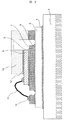
- an insulating layer 5 such as a ceramic substrate bonded to the upper surface of a base metal 3 via a first adhesive layer 4
- the insulating layer 5 is provided with a metal wiring 7 bonded to the upper surface of 5 via a second adhesive layer 6 and a semiconductor chip 9 bonded to the metal wiring 7 via a third adhesive layer 8.
- the first, second and third adhesive layers contain vanadium oxide glass and metal particles.
- the insulating layer 5 include a ceramic substrate having high thermal conductivity such as AlN and Si 3 N 4 .
- first, second and third adhesive layers are included in the semiconductor module of the present invention, but the present invention can naturally be applied to only one of the first, second or third adhesive layers. It is.
- the adhesive member may be provided between the members to be bonded.
- the area of the bonding member is smaller than the area of the smaller bonding surface (the metal wiring 7 in the insulating layer 5 and the metal wiring 7 and the semiconductor chip 9 in the metal wiring 7 and the semiconductor chip 9).
- the area of the adhesive member may be smaller than the area of the smaller adhesive surface.
- each member may be in contact with the adhesive member on at least one surface, but even if the adhesive layer extends to a plurality of surfaces such as side surfaces, the members can be bonded more firmly.
- a power device As a semiconductor module, for example, a power device can be cited, and it may be installed in a place where a large vibration or a long-term vibration is applied or a place exposed to a high temperature. Therefore, each part needs to be firmly bonded to each other.
- the softened vanadium oxide glass adheres to and solidifies with each component with high wettability, so that each of the base metal 3, the insulating layer 5, the metal wiring 7, and the semiconductor chip 9 can be firmly bonded. Therefore, even if ceramics are included in the parts, the adhesion between the parts can be improved without performing metallization.
- the adhesive member used in the semiconductor module needs to be able to dissipate heat through the adhesive part. Therefore, the adhesive member of the present invention contains metal particles to increase the thermal conductivity of the adhesive.
- the glass contained in the adhesive member contains V 2 O 5 .
- V 2 O 5 is 35 to 55% by mass
- TeO 2 is 15 to 35% by mass
- P 2 O 5 is 4 to 20% by mass
- At least one of Sb 2 O 3 , Bi 2 O 3 , BaO, K 2 O, and ZnO is 5 to 30% by mass. Since glass having such a composition range has a glass transition point of 330 ° C. or lower and sufficiently softens even at a temperature of 500 ° C. or lower, all of the base metal 3, the insulating layer 5, the metal wiring 7, and the semiconductor chip 9 are good. Can be adhered to.
- glass is an oxide, so when mixed and heated, the metal particles are oxidized in most cases.
- the vanadium oxide glass constituting the present invention is mixed with a metal powder such as Cu, Fe, or Al and heated, the metal powder is oxidized.
- Ag is known as a metal that is difficult to oxidize, and is not oxidized even when mixed with the vanadium oxide glass constituting the present invention and heated.
- Sn-based lead-free solder Sn—Ag—Cu-based solder or Sn—Cu—Ni-based solder
- the metal particles may contain at least one of Ag or Sn-containing solder (Sn—Ag—Cu solder). Since Ag or Sn-containing solder is not easily oxidized even when mixed with vanadium oxide glass, the thermal conductivity when the adhesive member is formed is unlikely to decrease.
- the second adhesive member 6 is not required to have conductivity, so that it may be Sn-containing solder powder or a mixture of both, in addition to Ag, which is a good electrical conductor.
- the metal particles may occupy 30 to 95% by volume of the second adhesive member 6. With such a configuration, the insulating layer 5 and the metal wiring 7 can be satisfactorily bonded and have an appropriate thermal conductivity. Further, when the metal particles occupy 60 to 95% by volume of the second adhesive member 6, the thermal conductivity is further improved, and the heat generation of the semiconductor chip 9 can be released more quickly.
- the glass may contain 10 to 60% by mass of Ag 2 O, 5 to 65% by mass of V 2 O 5 , and 15 to 50% by mass of TeO 2 . By making such a composition range, the glass transition point can be further lowered to 250 ° C. or lower, and sufficient thermal stability can be ensured. Any of the layer 5, the metal wiring 7, and the semiconductor chip 9 can be bonded well.
- the semiconductor module in which the present invention is applied only to the third adhesive layer 8 includes a semiconductor chip 9 bonded to the metal wiring 7 via the third adhesive layer 8.
- the third adhesive member 8 contains vanadium oxide glass and metal particles.
- the metal particles are Ag and occupy 60 to 95% by volume of the third adhesive member 8.
- the adhesive member of the present invention can be used. That is, in the semiconductor module having the above-described configuration, the semiconductor chip 9 and the metal wiring 7 are connected by the metal members 10 and 11 via the fourth adhesive member 12 and the fifth adhesive member 13.
- the metal particles are Ag, and occupy 60 to 95% by volume of the fourth adhesive member.
- composition of the vanadium oxide glass of the third adhesive member 8, the fourth adhesive member 12, and the fifth adhesive member 13 can be the same as that of the second adhesive member 6.
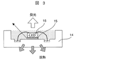
- FIG. 3 shows a sectional view of the structure of an LED lighting device.
- the LED lighting device includes a light emitting module in which an LED light emitting element 16 is bonded to a substrate 14 via an adhesive member 15, and a power supply circuit unit (not shown) that supplies power to the light emitting module.
- the adhesive member 15 is the same as that of the semiconductor module.
- ⁇ LED light emitting elements are easily deteriorated by heat, so heat generated by light emission must be quickly released to the outside. For this reason, when the metal particles are made of Ag and occupy 60 to 95% by volume of the adhesive member, the substrate and the LED light-emitting element can be favorably bonded and have high thermal conductivity.
- FIG. 4 shows a semiconductor device such as a personal computer motherboard.
- the semiconductor device includes a microcomputer IC in which a CPU 19 is connected to a heat sink 20 via an adhesive member 18 on a substrate 17.
- the adhesive member 18 is the same as that of the semiconductor module.
- the glass contained in the adhesive member 18 includes V 2 O 5 of 35 to 55% by mass, TeO 2 of 15 to 35% by mass, P 2 O 5 of 4 to 20% by mass, and Fe 2 O 3 ,
- One or more of WO 3 , MoO 3 , MnO 2 , Sb 2 O 3 , Bi 2 O 3 , BaO, K 2 O, and ZnO is 5 to 30% by mass. Since glass having such a composition range has a glass transition point of 330 ° C. or lower, it is sufficiently softened even at a temperature of 500 ° C. or lower, so that the substrate and the LED light emitting element or the CPU and the heat sink are good at a temperature of 500 ° C. or lower. Can be adhered to.
- the glass transition point can be lowered to 250 ° C. or lower, and sufficient thermal stability can be secured, and the substrate and the LED light emitting element at a temperature of 400 ° C. or lower, Alternatively, the CPU and the heat sink can be favorably bonded.
- vanadium oxide glasses having various compositions were prepared, and the softening point and moisture resistance of the glass were investigated.
- Each starting material powder was mixed at a mass ratio shown in Table 1, and a total of 200 g of the mixed powder was put in a crucible.
- a platinum crucible was used when the Ag 2 O ratio in the raw material was 40% by mass or less, and an alumina crucible was used when the proportion was 40% by mass or more.
- mixing in consideration of avoiding excessive moisture absorption to the raw material powder, mixing was performed in a crucible using a metal spoon.
- the crucible containing the raw material mixed powder was placed in a glass melting furnace and heated and melted. The temperature was raised at a rate of 10 ° C./min, and the molten glass was held for 1 hour with stirring at the set temperature (700 to 900 ° C.). Thereafter, the crucible was taken out from the glass melting furnace, and the glass was cast into a graphite mold heated to 150 ° C. in advance. Next, the cast glass was moved to a strain relief furnace that had been heated to a strain relief temperature in advance, strain was removed by holding for 1 hour, and then cooled to room temperature at a rate of 1 ° C./min. The glass cooled to room temperature was pulverized to produce glass powder having the composition shown in the table.
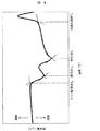
- the characteristic temperature was measured by differential thermal analysis (DTA) with respect to each glass powder obtained above.
- the DTA measurement was performed at a temperature increase rate of 5 ° C./min in the atmosphere with the reference sample ( ⁇ -alumina) and the measurement sample weighing 650 mg each.
- the second endothermic peak temperature of the DTA curve of the glass was defined as the softening point Ts (see FIG. 5). The results are also shown in Table 1.
- VTC2-01 was pulverized into a fine powder having an average particle size of 0.5 ⁇ m or less.
- the pulverized VTC2-01 and Ag powder or Sn—Ag—Cu solder powder were mixed at a predetermined ratio, and mixed for 15 minutes with a mortar to prepare a mixed powder.
- Thermal conductivity of Various mixed powders were formed into molded bodies having a diameter of 10 mm and a thickness of 2 mm using a mold. Using the electric muffle furnace, the produced molded body was fired at 450 ° C. for 30 minutes in the atmosphere, and used as a simulated sample for evaluating the thermal conductivity of the first adhesive layer. Using the sintered body sample thus produced, the thermal conductivity was measured by the xenon flash method.
- the xenon flash method is a method in which one side of a simulated sample is irradiated with pulsed light, and the thermal diffusivity is measured from the time change of the back surface temperature, and the thermal conductivity is calculated based on this.
- the thermal conductivity of each sample is summarized in Table 2.
- a die bonding material paste was printed on a ceramic substrate in a range of 5 ⁇ 5 mm 2 , dried at 150 ° C., and then pre-fired in air at 450 ° C. for 30 minutes. Thereafter, a Cu, Al, AlSiC plate cut out to 4 ⁇ 4 mm 2 was placed on the die bonding material, and 100 g of a weight was placed thereon, followed by firing at 450 ° C. for 30 minutes in the atmosphere.
- a die shear test sample in which a metal plate was bonded to a ceramic substrate was produced.
- the bond strength between the metal plate and the ceramic substrate was evaluated by a die shear strength test.
- the die shear strength test is performed by pressing a metal plate 18 joined on a substrate via an adhesive member 17 in a horizontal direction from the side by a dedicated jig 19, and the metal plate is peeled off from the substrate.
- This is a test method for measuring the load value, that is, the shear strength (die shear strength; N) of the metal plate.
- Table 2 summarizes the evaluation results when an AlN substrate is used as the ceramic substrate
- Table 3 summarizes the evaluation results when an Si 3 N 4 substrate is used.
- a sample having an adhesive strength> 20 Mpa and a thermal conductivity> 10 W / mK was accepted.
- the die bonding material of the example can bond a metal plate to a ceramic substrate without a metallized layer with high thermal conductivity and adhesive strength.
- VTC3-01 was pulverized into a fine powder having an average particle size of 0.5 ⁇ m or less.
- the ground VTC3-01 and Ag powder were blended at a predetermined ratio, and mixed for 15 minutes with a mortar to prepare a mixed powder.
- Thermal conductivity and electrical resistivity Various mixed powders were formed into molded bodies having a diameter of 10 mm and a thickness of 2 mm using a mold. Using the electric muffle furnace, the produced molded body was fired at 350 ° C. for 30 minutes in the atmosphere, and used as a simulation sample for evaluating the thermal conductivity and electrical resistivity of the third adhesive layer.
- the electrical resistivity of the sintered body sample was measured using a simple low resistivity meter (Loresta AX; MCP-T370 type) manufactured by Mitsubishi Chemical Corporation. Thereafter, the thermal conductivity was measured by the xenon flash method using the same sample.
- a die bonding material paste (Adhesive strength) Various mixed powders, a resin binder, and a solvent were mixed to prepare a die bonding material paste in the same manner as in Example 2.
- a die bonding material paste was printed on a ceramic substrate in a range of 5 ⁇ 5 mm 2 , dried at 150 ° C., and then pre-fired at 350 ° C. for 30 minutes in the air. Thereafter, a 4 ⁇ 4 mm 2 Si semiconductor chip is placed on the die bonding material, a 100 g weight is placed on the die bonding material, fired at 350 ° C. for 30 minutes in the air, and the Si semiconductor chip is bonded to the Cu substrate. It was.
- the bond strength between the Si semiconductor chip and the Cu substrate was evaluated by a die shear strength test. Table 4 summarizes the evaluation results.
- the die bonding material of the example can be bonded to a ceramic substrate having no metallized layer with high thermal conductivity and adhesive strength.
Landscapes
- Chemical & Material Sciences (AREA)
- Engineering & Computer Science (AREA)
- Materials Engineering (AREA)
- Ceramic Engineering (AREA)
- Organic Chemistry (AREA)
- Mechanical Engineering (AREA)
- Metallurgy (AREA)
- Structural Engineering (AREA)
- Die Bonding (AREA)
- Glass Compositions (AREA)
- Ceramic Products (AREA)
- Electric Connection Of Electric Components To Printed Circuits (AREA)
- Structure Of Printed Boards (AREA)
Priority Applications (4)
| Application Number | Priority Date | Filing Date | Title |
|---|---|---|---|
| KR1020147018264A KR101572774B1 (ko) | 2012-01-26 | 2012-11-21 | 접합체 및 반도체 모듈 |
| DE112012005758.9T DE112012005758B4 (de) | 2012-01-26 | 2012-11-21 | Gebondetes Bauelement und Halbleitermodul |
| US14/374,396 US9196563B2 (en) | 2012-01-26 | 2012-11-21 | Bonded body and semiconductor module |
| CN201280060767.2A CN104159872A (zh) | 2012-01-26 | 2012-11-21 | 接合体及半导体模块 |
Applications Claiming Priority (2)
| Application Number | Priority Date | Filing Date | Title |
|---|---|---|---|
| JP2012-013663 | 2012-01-26 | ||
| JP2012013663A JP5732414B2 (ja) | 2012-01-26 | 2012-01-26 | 接合体および半導体モジュール |
Publications (1)
| Publication Number | Publication Date |
|---|---|
| WO2013111434A1 true WO2013111434A1 (ja) | 2013-08-01 |
Family
ID=48873175
Family Applications (1)
| Application Number | Title | Priority Date | Filing Date |
|---|---|---|---|
| PCT/JP2012/080121 Ceased WO2013111434A1 (ja) | 2012-01-26 | 2012-11-21 | 接合体および半導体モジュール |
Country Status (7)
| Country | Link |
|---|---|
| US (1) | US9196563B2 (https=) |
| JP (1) | JP5732414B2 (https=) |
| KR (1) | KR101572774B1 (https=) |
| CN (1) | CN104159872A (https=) |
| DE (1) | DE112012005758B4 (https=) |
| TW (1) | TWI489594B (https=) |
| WO (1) | WO2013111434A1 (https=) |
Cited By (3)
| Publication number | Priority date | Publication date | Assignee | Title |
|---|---|---|---|---|
| WO2016043095A1 (ja) * | 2014-09-19 | 2016-03-24 | 株式会社日立製作所 | 放熱構造体及びそれを利用した半導体モジュール |
| CN105683111A (zh) * | 2013-12-04 | 2016-06-15 | 株式会社日立制作所 | 密封结构体、多层隔热玻璃、玻璃容器 |
| WO2018121219A1 (zh) * | 2016-12-29 | 2018-07-05 | 比亚迪股份有限公司 | 散热基板及其制备方法和应用以及电子元器件 |
Families Citing this family (11)
| Publication number | Priority date | Publication date | Assignee | Title |
|---|---|---|---|---|
| JP5726698B2 (ja) | 2011-07-04 | 2015-06-03 | 株式会社日立製作所 | ガラス組成物、それを含むガラスフリット、それを含むガラスペースト、およびそれを利用した電気電子部品 |
| JP5844299B2 (ja) | 2013-03-25 | 2016-01-13 | 株式会社日立製作所 | 接合材、接合構造体 |
| KR102225427B1 (ko) * | 2013-12-25 | 2021-03-08 | 미쓰비시 마테리알 가부시키가이샤 | 파워 모듈용 기판 및 그 제조 방법, 파워 모듈 |
| EP3236495B1 (en) * | 2014-12-16 | 2019-09-11 | Kyocera Corporation | Circuit substrate and electronic device |
| DE102015104518B3 (de) * | 2015-03-25 | 2016-03-10 | Infineon Technologies Ag | Verfahren zur Herstellung einer Schaltungsträgeranordnung mit einem Träger, der eine durch ein Aluminium-Siliziumkarbid-Metallmatrixkompositmaterial gebildete Oberfläche aufweist |
| CN107408514B (zh) * | 2015-04-09 | 2020-04-14 | 纳美仕有限公司 | 接合体的制造方法 |
| CN106025054A (zh) * | 2016-06-29 | 2016-10-12 | 海宁市智慧光电有限公司 | 一种高可靠性超亮片式led光源 |
| US20190074416A1 (en) * | 2017-09-06 | 2019-03-07 | Coorstek Kk | Silica glass member, process for producing the same, and process for bonding ceramic and silica glass |
| CN107683016A (zh) * | 2017-11-21 | 2018-02-09 | 生益电子股份有限公司 | 一种快速散热pcb |
| KR102217222B1 (ko) * | 2019-01-30 | 2021-02-19 | 엘지전자 주식회사 | 무연계 저온 소성 글라스 프릿, 페이스트 및 이를 이용한 진공 유리 조립체 |
| DE102023108698A1 (de) * | 2023-04-05 | 2024-10-10 | Danfoss Silicon Power Gmbh | Baugruppe zur Bereitstellung elektronischer Funktionalitäten und Mittel zur Qualitätssicherung einer Fixierschicht davon |
Citations (3)
| Publication number | Priority date | Publication date | Assignee | Title |
|---|---|---|---|---|
| JPH02293344A (ja) * | 1989-04-19 | 1990-12-04 | Natl Starch & Chem Corp | 電子的用途に使用するのに好適な低軟化点金属酸化物ガラス |
| JPH05175254A (ja) * | 1991-12-20 | 1993-07-13 | Nippon Electric Glass Co Ltd | 低融点接着組成物 |
| JP2010184852A (ja) * | 2009-01-16 | 2010-08-26 | Hitachi Powdered Metals Co Ltd | 低融点ガラス組成物、それを用いた低温封着材料及び電子部品 |
Family Cites Families (11)
| Publication number | Priority date | Publication date | Assignee | Title |
|---|---|---|---|---|
| US5188990A (en) * | 1991-11-21 | 1993-02-23 | Vlsi Packaging Materials | Low temperature sealing glass compositions |
| JPH08107166A (ja) * | 1994-10-06 | 1996-04-23 | Mitsubishi Materials Corp | 放熱用フィン |
| JPH08259262A (ja) | 1995-03-20 | 1996-10-08 | Nippon Electric Glass Co Ltd | 低融点封着用組成物 |
| TWI224382B (en) * | 2001-07-12 | 2004-11-21 | Hitachi Ltd | Wiring glass substrate and manufacturing method thereof, conductive paste and semiconductor module used for the same, and conductor forming method |
| US6717276B2 (en) * | 2002-09-10 | 2004-04-06 | Texas Instruments Incorporated | Two-metal layer ball grid array and chip scale package having local interconnects used in wire-bonded and flip-chip semiconductor assembly |
| CN101164942A (zh) * | 2006-10-19 | 2008-04-23 | 北京印刷学院 | 一种无铅碲酸盐低熔封接玻璃 |
| JP5609875B2 (ja) * | 2009-07-31 | 2014-10-22 | 旭硝子株式会社 | 半導体デバイス用封着ガラス、封着材料、封着材料ペースト、および半導体デバイスとその製造方法 |
| JP2011251329A (ja) | 2010-06-04 | 2011-12-15 | Sumitomo Metal Mining Co Ltd | 高温鉛フリーはんだペースト |
| TWI448444B (zh) | 2010-08-11 | 2014-08-11 | Hitachi Ltd | A glass composition for an electrode, a paste for an electrode for use, and an electronic component to which the electrode is used |
| JP5726698B2 (ja) | 2011-07-04 | 2015-06-03 | 株式会社日立製作所 | ガラス組成物、それを含むガラスフリット、それを含むガラスペースト、およびそれを利用した電気電子部品 |
| JP5519715B2 (ja) | 2012-02-07 | 2014-06-11 | 株式会社日立製作所 | 接合用無鉛ガラスおよびこの接合用無鉛ガラスを用いた平板型ディスプレイ装置 |
-
2012
- 2012-01-26 JP JP2012013663A patent/JP5732414B2/ja not_active Expired - Fee Related
- 2012-11-21 WO PCT/JP2012/080121 patent/WO2013111434A1/ja not_active Ceased
- 2012-11-21 DE DE112012005758.9T patent/DE112012005758B4/de not_active Expired - Fee Related
- 2012-11-21 KR KR1020147018264A patent/KR101572774B1/ko not_active Expired - Fee Related
- 2012-11-21 CN CN201280060767.2A patent/CN104159872A/zh active Pending
- 2012-11-21 US US14/374,396 patent/US9196563B2/en not_active Expired - Fee Related
- 2012-12-19 TW TW101148329A patent/TWI489594B/zh not_active IP Right Cessation
Patent Citations (3)
| Publication number | Priority date | Publication date | Assignee | Title |
|---|---|---|---|---|
| JPH02293344A (ja) * | 1989-04-19 | 1990-12-04 | Natl Starch & Chem Corp | 電子的用途に使用するのに好適な低軟化点金属酸化物ガラス |
| JPH05175254A (ja) * | 1991-12-20 | 1993-07-13 | Nippon Electric Glass Co Ltd | 低融点接着組成物 |
| JP2010184852A (ja) * | 2009-01-16 | 2010-08-26 | Hitachi Powdered Metals Co Ltd | 低融点ガラス組成物、それを用いた低温封着材料及び電子部品 |
Cited By (8)
| Publication number | Priority date | Publication date | Assignee | Title |
|---|---|---|---|---|
| CN105683111A (zh) * | 2013-12-04 | 2016-06-15 | 株式会社日立制作所 | 密封结构体、多层隔热玻璃、玻璃容器 |
| EP3078643A4 (en) * | 2013-12-04 | 2017-07-26 | Hitachi, Ltd. | Sealed structure, multi-layer heat-insulating glass and glass container |
| US10392296B2 (en) | 2013-12-04 | 2019-08-27 | Hitachi, Ltd. | Sealed structural body and method for manufacturing the same |
| WO2016043095A1 (ja) * | 2014-09-19 | 2016-03-24 | 株式会社日立製作所 | 放熱構造体及びそれを利用した半導体モジュール |
| JPWO2016043095A1 (ja) * | 2014-09-19 | 2017-05-25 | 株式会社日立製作所 | 放熱構造体及びそれを利用した半導体モジュール |
| US10177069B2 (en) | 2014-09-19 | 2019-01-08 | Hitachi Ltd. | Heat-dissipating structure and semiconductor module using same |
| WO2018121219A1 (zh) * | 2016-12-29 | 2018-07-05 | 比亚迪股份有限公司 | 散热基板及其制备方法和应用以及电子元器件 |
| CN108257929A (zh) * | 2016-12-29 | 2018-07-06 | 比亚迪股份有限公司 | 一种散热基板及其制备方法和应用以及电子元器件 |
Also Published As
| Publication number | Publication date |
|---|---|
| KR101572774B1 (ko) | 2015-11-27 |
| JP2013151396A (ja) | 2013-08-08 |
| DE112012005758T5 (de) | 2014-11-20 |
| TW201347102A (zh) | 2013-11-16 |
| KR20140104469A (ko) | 2014-08-28 |
| JP5732414B2 (ja) | 2015-06-10 |
| US9196563B2 (en) | 2015-11-24 |
| US20150008573A1 (en) | 2015-01-08 |
| TWI489594B (zh) | 2015-06-21 |
| DE112012005758B4 (de) | 2017-05-24 |
| CN104159872A (zh) | 2014-11-19 |
Similar Documents
| Publication | Publication Date | Title |
|---|---|---|
| JP5732414B2 (ja) | 接合体および半導体モジュール | |
| KR102066300B1 (ko) | 땜납 접합 구조, 파워 모듈, 히트 싱크가 형성된 파워 모듈용 기판 및 그것들의 제조 방법, 그리고 땜납 하지층 형성용 페이스트 | |
| JP5346272B2 (ja) | 素子搭載基板及び発光装置 | |
| JP6560684B2 (ja) | 導電性ペースト及びそれを用いた半導体装置の製造方法 | |
| JP2010287869A (ja) | パワーモジュール用基板、冷却器付パワーモジュール用基板、パワーモジュール及びパワーモジュール用基板の製造方法 | |
| JP5304508B2 (ja) | 導電性組成物 | |
| WO2014119579A1 (ja) | ガラスフリット | |
| JPWO2012036219A1 (ja) | 発光素子用基板および発光装置 | |
| CN104072187A (zh) | 接合材料和接合构造体 | |
| KR102225427B1 (ko) | 파워 모듈용 기판 및 그 제조 방법, 파워 모듈 | |
| CN103680677A (zh) | 低烧制温度的铜组合物 | |
| TW201428070A (zh) | 接合構造體及其製造方法 | |
| CN102640310A (zh) | 发光元件用基板及发光装置 | |
| JP2018109073A (ja) | 複合材組成物、及びそれを用いたペースト剤 | |
| TW201234540A (en) | Substrate for light-emitting element, and light-emitting device | |
| US20170294399A1 (en) | POWER MODULE SUBSTRATE WITH Ag UNDERLAYER AND POWER MODULE | |
| WO2018062373A1 (ja) | 抵抗体およびこれを備える回路基板ならびに電子装置 | |
| JP5356305B2 (ja) | 絶縁層を有する高熱伝導性基板ならびに該絶縁層形成用材料 | |
| JP5941006B2 (ja) | 接合材、接合構造体およびその製造方法、並びに半導体モジュール | |
| TWI691580B (zh) | 接合體之製造方法 | |
| JP3699571B2 (ja) | 配線基板およびその実装構造 | |
| JP3323074B2 (ja) | 配線基板、半導体素子収納用パッケージおよびその実装構造 | |
| JP6204212B2 (ja) | 熱伝導複合材料 | |
| JP2013157389A (ja) | 回路基板およびこれを備える電子装置 |
Legal Events
| Date | Code | Title | Description |
|---|---|---|---|
| 121 | Ep: the epo has been informed by wipo that ep was designated in this application |
Ref document number: 12866658 Country of ref document: EP Kind code of ref document: A1 |
|
| ENP | Entry into the national phase |
Ref document number: 20147018264 Country of ref document: KR Kind code of ref document: A |
|
| WWE | Wipo information: entry into national phase |
Ref document number: 14374396 Country of ref document: US |
|
| WWE | Wipo information: entry into national phase |
Ref document number: 112012005758 Country of ref document: DE Ref document number: 1120120057589 Country of ref document: DE |
|
| 122 | Ep: pct application non-entry in european phase |
Ref document number: 12866658 Country of ref document: EP Kind code of ref document: A1 |