WO2013099194A1 - 半導体装置およびその製造方法 - Google Patents
半導体装置およびその製造方法 Download PDFInfo
- Publication number
- WO2013099194A1 WO2013099194A1 PCT/JP2012/008217 JP2012008217W WO2013099194A1 WO 2013099194 A1 WO2013099194 A1 WO 2013099194A1 JP 2012008217 W JP2012008217 W JP 2012008217W WO 2013099194 A1 WO2013099194 A1 WO 2013099194A1
- Authority
- WO
- WIPO (PCT)
- Prior art keywords
- mother substrate
- semiconductor device
- components
- parts
- module
- Prior art date
- Legal status (The legal status is an assumption and is not a legal conclusion. Google has not performed a legal analysis and makes no representation as to the accuracy of the status listed.)
- Ceased
Links
Images


Classifications
-
- H—ELECTRICITY
- H10—SEMICONDUCTOR DEVICES; ELECTRIC SOLID-STATE DEVICES NOT OTHERWISE PROVIDED FOR
- H10W—GENERIC PACKAGES, INTERCONNECTIONS, CONNECTORS OR OTHER CONSTRUCTIONAL DETAILS OF DEVICES COVERED BY CLASS H10
- H10W74/00—Encapsulations, e.g. protective coatings
-
- H—ELECTRICITY
- H10—SEMICONDUCTOR DEVICES; ELECTRIC SOLID-STATE DEVICES NOT OTHERWISE PROVIDED FOR
- H10W—GENERIC PACKAGES, INTERCONNECTIONS, CONNECTORS OR OTHER CONSTRUCTIONAL DETAILS OF DEVICES COVERED BY CLASS H10
- H10W90/00—Package configurations
-
- H—ELECTRICITY
- H05—ELECTRIC TECHNIQUES NOT OTHERWISE PROVIDED FOR
- H05K—PRINTED CIRCUITS; CASINGS OR CONSTRUCTIONAL DETAILS OF ELECTRIC APPARATUS; MANUFACTURE OF ASSEMBLAGES OF ELECTRICAL COMPONENTS
- H05K1/00—Printed circuits
- H05K1/02—Details
- H05K1/14—Structural association of two or more printed circuits
- H05K1/141—One or more single auxiliary printed circuits mounted on a main printed circuit, e.g. modules, adapters
-
- H—ELECTRICITY
- H05—ELECTRIC TECHNIQUES NOT OTHERWISE PROVIDED FOR
- H05K—PRINTED CIRCUITS; CASINGS OR CONSTRUCTIONAL DETAILS OF ELECTRIC APPARATUS; MANUFACTURE OF ASSEMBLAGES OF ELECTRICAL COMPONENTS
- H05K1/00—Printed circuits
- H05K1/18—Printed circuits structurally associated with non-printed electric components
-
- H—ELECTRICITY
- H10—SEMICONDUCTOR DEVICES; ELECTRIC SOLID-STATE DEVICES NOT OTHERWISE PROVIDED FOR
- H10W—GENERIC PACKAGES, INTERCONNECTIONS, CONNECTORS OR OTHER CONSTRUCTIONAL DETAILS OF DEVICES COVERED BY CLASS H10
- H10W70/00—Package substrates; Interposers; Redistribution layers [RDL]
- H10W70/60—Insulating or insulated package substrates; Interposers; Redistribution layers
- H10W70/62—Insulating or insulated package substrates; Interposers; Redistribution layers characterised by their interconnections
- H10W70/65—Shapes or dispositions of interconnections
- H10W70/657—Shapes or dispositions of interconnections on sidewalls or bottom surfaces of the package substrates, interposers or redistribution layers
-
- H—ELECTRICITY
- H10—SEMICONDUCTOR DEVICES; ELECTRIC SOLID-STATE DEVICES NOT OTHERWISE PROVIDED FOR
- H10W—GENERIC PACKAGES, INTERCONNECTIONS, CONNECTORS OR OTHER CONSTRUCTIONAL DETAILS OF DEVICES COVERED BY CLASS H10
- H10W70/00—Package substrates; Interposers; Redistribution layers [RDL]
- H10W70/60—Insulating or insulated package substrates; Interposers; Redistribution layers
- H10W70/67—Insulating or insulated package substrates; Interposers; Redistribution layers characterised by their insulating layers or insulating parts
- H10W70/68—Shapes or dispositions thereof
-
- H—ELECTRICITY
- H10—SEMICONDUCTOR DEVICES; ELECTRIC SOLID-STATE DEVICES NOT OTHERWISE PROVIDED FOR
- H10W—GENERIC PACKAGES, INTERCONNECTIONS, CONNECTORS OR OTHER CONSTRUCTIONAL DETAILS OF DEVICES COVERED BY CLASS H10
- H10W74/00—Encapsulations, e.g. protective coatings
- H10W74/01—Manufacture or treatment
- H10W74/012—Manufacture or treatment of encapsulations on active surfaces of flip-chip devices, e.g. forming underfills
-
- H—ELECTRICITY
- H10—SEMICONDUCTOR DEVICES; ELECTRIC SOLID-STATE DEVICES NOT OTHERWISE PROVIDED FOR
- H10W—GENERIC PACKAGES, INTERCONNECTIONS, CONNECTORS OR OTHER CONSTRUCTIONAL DETAILS OF DEVICES COVERED BY CLASS H10
- H10W74/00—Encapsulations, e.g. protective coatings
- H10W74/10—Encapsulations, e.g. protective coatings characterised by their shape or disposition
- H10W74/15—Encapsulations, e.g. protective coatings characterised by their shape or disposition on active surfaces of flip-chip devices, e.g. underfills
-
- H—ELECTRICITY
- H10—SEMICONDUCTOR DEVICES; ELECTRIC SOLID-STATE DEVICES NOT OTHERWISE PROVIDED FOR
- H10W—GENERIC PACKAGES, INTERCONNECTIONS, CONNECTORS OR OTHER CONSTRUCTIONAL DETAILS OF DEVICES COVERED BY CLASS H10
- H10W76/00—Containers; Fillings or auxiliary members therefor; Seals
- H10W76/10—Containers or parts thereof
- H10W76/12—Containers or parts thereof characterised by their shape
- H10W76/15—Containers comprising an insulating or insulated base
-
- H—ELECTRICITY
- H05—ELECTRIC TECHNIQUES NOT OTHERWISE PROVIDED FOR
- H05K—PRINTED CIRCUITS; CASINGS OR CONSTRUCTIONAL DETAILS OF ELECTRIC APPARATUS; MANUFACTURE OF ASSEMBLAGES OF ELECTRICAL COMPONENTS
- H05K2201/00—Indexing scheme relating to printed circuits covered by H05K1/00
- H05K2201/04—Assemblies of printed circuits
- H05K2201/042—Stacked spaced PCBs; Planar parts of folded flexible circuits having mounted components in between or spaced from each other
-
- H—ELECTRICITY
- H05—ELECTRIC TECHNIQUES NOT OTHERWISE PROVIDED FOR
- H05K—PRINTED CIRCUITS; CASINGS OR CONSTRUCTIONAL DETAILS OF ELECTRIC APPARATUS; MANUFACTURE OF ASSEMBLAGES OF ELECTRICAL COMPONENTS
- H05K2201/00—Indexing scheme relating to printed circuits covered by H05K1/00
- H05K2201/10—Details of components or other objects attached to or integrated in a printed circuit board
- H05K2201/10613—Details of electrical connections of non-printed components, e.g. special leads
- H05K2201/10621—Components characterised by their electrical contacts
- H05K2201/10636—Leadless chip, e.g. chip capacitor or resistor
-
- H—ELECTRICITY
- H05—ELECTRIC TECHNIQUES NOT OTHERWISE PROVIDED FOR
- H05K—PRINTED CIRCUITS; CASINGS OR CONSTRUCTIONAL DETAILS OF ELECTRIC APPARATUS; MANUFACTURE OF ASSEMBLAGES OF ELECTRICAL COMPONENTS
- H05K2201/00—Indexing scheme relating to printed circuits covered by H05K1/00
- H05K2201/20—Details of printed circuits not provided for in H05K2201/01 - H05K2201/10
- H05K2201/2036—Permanent spacer or stand-off in a printed circuit or printed circuit assembly
-
- H—ELECTRICITY
- H10—SEMICONDUCTOR DEVICES; ELECTRIC SOLID-STATE DEVICES NOT OTHERWISE PROVIDED FOR
- H10W—GENERIC PACKAGES, INTERCONNECTIONS, CONNECTORS OR OTHER CONSTRUCTIONAL DETAILS OF DEVICES COVERED BY CLASS H10
- H10W40/00—Arrangements for thermal protection or thermal control
- H10W40/10—Arrangements for heating
-
- H—ELECTRICITY
- H10—SEMICONDUCTOR DEVICES; ELECTRIC SOLID-STATE DEVICES NOT OTHERWISE PROVIDED FOR
- H10W—GENERIC PACKAGES, INTERCONNECTIONS, CONNECTORS OR OTHER CONSTRUCTIONAL DETAILS OF DEVICES COVERED BY CLASS H10
- H10W40/00—Arrangements for thermal protection or thermal control
- H10W40/70—Fillings or auxiliary members in containers or in encapsulations for thermal protection or control
-
- H—ELECTRICITY
- H10—SEMICONDUCTOR DEVICES; ELECTRIC SOLID-STATE DEVICES NOT OTHERWISE PROVIDED FOR
- H10W—GENERIC PACKAGES, INTERCONNECTIONS, CONNECTORS OR OTHER CONSTRUCTIONAL DETAILS OF DEVICES COVERED BY CLASS H10
- H10W70/00—Package substrates; Interposers; Redistribution layers [RDL]
- H10W70/60—Insulating or insulated package substrates; Interposers; Redistribution layers
- H10W70/67—Insulating or insulated package substrates; Interposers; Redistribution layers characterised by their insulating layers or insulating parts
- H10W70/68—Shapes or dispositions thereof
- H10W70/681—Shapes or dispositions thereof comprising holes not having chips therein, e.g. for outgassing, underfilling or bond wire passage
-
- H—ELECTRICITY
- H10—SEMICONDUCTOR DEVICES; ELECTRIC SOLID-STATE DEVICES NOT OTHERWISE PROVIDED FOR
- H10W—GENERIC PACKAGES, INTERCONNECTIONS, CONNECTORS OR OTHER CONSTRUCTIONAL DETAILS OF DEVICES COVERED BY CLASS H10
- H10W70/00—Package substrates; Interposers; Redistribution layers [RDL]
- H10W70/60—Insulating or insulated package substrates; Interposers; Redistribution layers
- H10W70/67—Insulating or insulated package substrates; Interposers; Redistribution layers characterised by their insulating layers or insulating parts
- H10W70/68—Shapes or dispositions thereof
- H10W70/682—Shapes or dispositions thereof comprising holes having chips therein
-
- H—ELECTRICITY
- H10—SEMICONDUCTOR DEVICES; ELECTRIC SOLID-STATE DEVICES NOT OTHERWISE PROVIDED FOR
- H10W—GENERIC PACKAGES, INTERCONNECTIONS, CONNECTORS OR OTHER CONSTRUCTIONAL DETAILS OF DEVICES COVERED BY CLASS H10
- H10W90/00—Package configurations
- H10W90/701—Package configurations characterised by the relative positions of pads or connectors relative to package parts
- H10W90/721—Package configurations characterised by the relative positions of pads or connectors relative to package parts of bump connectors
- H10W90/724—Package configurations characterised by the relative positions of pads or connectors relative to package parts of bump connectors between a chip and a stacked insulating package substrate, interposer or RDL
-
- H—ELECTRICITY
- H10—SEMICONDUCTOR DEVICES; ELECTRIC SOLID-STATE DEVICES NOT OTHERWISE PROVIDED FOR
- H10W—GENERIC PACKAGES, INTERCONNECTIONS, CONNECTORS OR OTHER CONSTRUCTIONAL DETAILS OF DEVICES COVERED BY CLASS H10
- H10W90/00—Package configurations
- H10W90/701—Package configurations characterised by the relative positions of pads or connectors relative to package parts
- H10W90/731—Package configurations characterised by the relative positions of pads or connectors relative to package parts of die-attach connectors
- H10W90/734—Package configurations characterised by the relative positions of pads or connectors relative to package parts of die-attach connectors between a chip and a stacked insulating package substrate, interposer or RDL
-
- Y—GENERAL TAGGING OF NEW TECHNOLOGICAL DEVELOPMENTS; GENERAL TAGGING OF CROSS-SECTIONAL TECHNOLOGIES SPANNING OVER SEVERAL SECTIONS OF THE IPC; TECHNICAL SUBJECTS COVERED BY FORMER USPC CROSS-REFERENCE ART COLLECTIONS [XRACs] AND DIGESTS
- Y02—TECHNOLOGIES OR APPLICATIONS FOR MITIGATION OR ADAPTATION AGAINST CLIMATE CHANGE
- Y02P—CLIMATE CHANGE MITIGATION TECHNOLOGIES IN THE PRODUCTION OR PROCESSING OF GOODS
- Y02P70/00—Climate change mitigation technologies in the production process for final industrial or consumer products
- Y02P70/50—Manufacturing or production processes characterised by the final manufactured product
Definitions
- the present invention relates to a semiconductor device provided with an electronic component in a cavity of a cavity structure module and a method of manufacturing the same.
- Patent Document 1 discloses a configuration in which an electronic component is mounted on the cavity side of a base substrate in a cavity structure module in which a cavity is formed by a base substrate and a support substrate.
- the mother substrate is bonded to the cavity side to complete the semiconductor device.
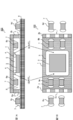
- FIG. 1 shows a configuration example of the above-described semiconductor device
- FIG. 1A is a cross-sectional view
- FIG. 1B is a view seen from a mother substrate side.
- the legs 2a and 2b in the vertical direction are illustrated, and the legs in the horizontal direction are omitted.
- the IC 3 and the chip parts 6a and 6b are mounted on the base substrate 1.
- the underfill 5 is filled between the IC 3 and the base substrate 1, but the underfill 5 protrudes around the IC 3.
- the underfill 5 protrudes around the IC 3, it is difficult to provide a chip component in the protruding portion, which is a wasteful space. As a result, the cavity structure module becomes large, and furthermore, in FIG. 1, it is necessary to arrange the chip parts 6c and 6d outside the cavity structure module. Therefore, the enlargement of the semiconductor device becomes a problem.
- An object of the present invention is to provide a semiconductor device in which an increase in size is suppressed and a method for manufacturing the same in a semiconductor device provided with an electronic component in a cavity of a cavity structure module.
- a semiconductor device is a semiconductor device including a structural module including a base substrate for arranging components and a leg portion, and a mother substrate joined to the leg portion, wherein the structural module is A plurality of components are provided on one surface facing the mother substrate, and the mother substrate is provided with the plurality of components on the surface provided with the plurality of components of the structural module among the surfaces facing the structural module Take a configuration in which parts are not provided.
- a method of manufacturing a semiconductor device is a method of manufacturing a semiconductor device including a structural module including a base substrate for arranging components and a leg portion, and a mother substrate joined to the leg portion, A plurality of components are mounted on one surface of the structural module facing the mother substrate, and one of the surfaces of the mother substrate facing the structural module on which the plurality of components of the structural module are provided A component is mounted on a portion where the plurality of components are not provided, and a surface of the structural module on which the components are mounted and a surface of the mother substrate on which the components are provided are bonded to face each other.
- an increase in size can be prevented in a semiconductor device including an electronic component in a cavity structure module.
- FIG. 5 illustrates an example of a process of a method of manufacturing a semiconductor device according to Embodiment 1 of the present invention.
- FIG. 2 is a side sectional view showing a configuration example of a semiconductor device according to Embodiment 1 of the present invention, and a view shown from below.
- FIG. 2 is a diagram showing an example of a process of the method of manufacturing a semiconductor device in the present embodiment.
- a “manufacturer” here may contain not only human but an apparatus, for example.
- FIG. 2F is a side view of the double-sided board.
- the base substrate 1 and the substrate 2 are bonded.
- FIG. 2A is a view showing the double-sided substrate from the substrate 2 side.
- the double-sided board is substantially square. Examples of the material of the base substrate 1 and the substrate 2 include glass epoxy.
- FIG. 2B shows the hollow portion indicated by the hatching in the substrate 2.
- FIG. 2C shows the formed legs 2a, 2b, 2c, 2d.
- a cavity structure module in which a space surrounded by the base substrate 1 and the legs 2a, 2b, 2c and 2d is a cavity is produced.
- FIG. 2G is a cross-sectional view taken along the line A-A 'shown in FIG. 2C (the same applies to FIGS. 2H and 2I described later).
- the legs 2c and 2d are not shown (the same applies to FIGS. 2H and 2I described later).
- the manufacturer forms a plurality of through holes connecting the outside and the inside of the cavity to the base substrate 1 of the created cavity structure module.
- through holes 10a, 10b, 10c and 10d are respectively formed at four corners of the base substrate 1 on the cavity side.
- the through holes 10a, 10b, 10c and 10d are used for evacuation or injection of a sealing resin. Therefore, in order to fill the cavity with the sealing resin without gaps, in FIG. 2D, it is preferable that one through hole be formed in each of the four corners, but the number or position of the through holes is not limited thereto. For example, in the case of forming two through holes, the four corners of the cavity side of the base substrate 1 may be formed diagonally. In FIG. 2D, it may be formed by a combination of the through hole 10a and the through hole 10d, or the combination of the through hole 10b and the through hole 10c.
- the manufacturer solders various electronic components on one surface (surface facing the mother substrate 9) of the cavity side of the base substrate 1 of the cavity structure module.
- the IC 3 and the chip parts 6a and 6b are mounted on the cavity side of the base substrate 1.
- the chip components 6 a and 6 b are mounted on the base substrate 1 by the solder 7.
- the IC 3 is mounted on the base substrate 1 through the solder balls 4, and the underfill 5 is filled between the IC 3 and the base substrate 1.
- the filled underfill 5 protrudes around the IC 3.
- the chip parts are not illustrated in FIG. 2E, but may be mounted other than 6a and 6b.
- the manufacturer solders the electronic component on the surface of the separately prepared mother substrate to be bonded to the cavity side of the cavity structure module.
- chip components 6 c and 6 d are mounted on the mother substrate 9 by the solder 7.
- the chip parts 6 c and 6 d are not mounted at arbitrary positions on the mother substrate 9. That is, when the mother substrate 9 and the cavity structure module are joined, the mounting positions of the chip components 6c and 6d correspond to (face) all or part of the portion where the underfill 5 protrudes on the base substrate 1 , The position on the mother substrate 9.
- the position on the mother board 9 corresponding to the space between the IC 3 and the chip part 6a is the mounting position of the chip part 6c, and the position on the mother board 9 corresponding to the space between the IC 3 and the chip part 6b. Is the mounting position of the chip part 6d.
- the manufacturer joins the cavity structure module on which the electronic component is mounted and the mother substrate 9 on which the electronic component is mounted. That is, the manufacturer causes the component mounting surface (surface on which the chip components 6c and 6d are mounted) of the mother substrate 9 to be opposed to and bonded to the cavity side of the cavity structure module. In bonding, the legs 2a, 2b, 2c, 2d and the mother substrate 9 are soldered (see FIG. 3A described later). Thereby, the cavity of the cavity structure module is sealed by the mother substrate 9.
- the manufacturer removes the air of the sealed cavity (for example, the space excluding the mounted electronic component) from, for example, the through holes 10a and 10c, and further injects the sealing resin from, for example, the through holes 10b and 10d. Do. Thereby, the cavity is filled with the sealing resin (see FIG. 3A described later).
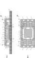
- FIG. 3A is a side sectional view taken along the line A-A 'in FIG. 2C
- FIG. 3B is a view showing the cavity structure module from the mother substrate 9 side.
- the leg 2c side and the leg 2d side are not shown.
- the cavity structure module is joined to the mother substrate 9 through the solder 7 attached to a part of the legs 2a, 2b, 2c, 2d. Further, a sealing resin 8 is filled in a cavity sealed by the mother substrate 9 (a space excluding the IC 3, the underfill 5, the chip components 6 a, 6 b, 6 c, 6 d and the solder 7). The sealing resin 8 is also filled in the through holes 10a, 10b, 10c, and 10d.
- the chip parts 6c and 6d which are conventionally mounted outside the cavity structure module (see FIG. 1) are mounted in the cavity structure module.
- the chip parts 6c and 6d are mounted in a space (a gap) which is a wasteful space due to the underfill 5 protruding.
- the mounting direction of the chip components 6c and 6d is vertical to the horizontal direction of the chip components 6a and 6b.
- FIG. 3 signal lines are built in the base substrate 1, the legs 2 a and 2 b, and the mother substrate 9. As a result, the IC 3 and the chip components 6 a, 6 b, 6 c, 6 d are electrically connected to the signal line via the solder ball 4 or the solder 7.
- the space in the cavity structure module is disposed by arranging the electronic component in the space of the portion where the underfill protrudes, which has not been used conventionally in the inside (cavity) of the cavity structure module. Is effectively used.
- the increase in size of the cavity structure module can be suppressed, and the number of electronic components disposed outside the cavity structure module can be reduced. Therefore, the enlargement of the semiconductor device can be suppressed.
- the cavity structure module mounting the electronic component without forming the through hole and the mother mounting the electronic component
- the substrate may be bonded.
- the cavity structure module it becomes difficult to inject the sealing resin inside the cavity structure module, but as described above, the electronic component is arranged in the space of the portion where the underfill which has not been used conventionally is protruded. The inner space can be used effectively.
- the electronic component mounted on the mother substrate has been described as the chip component (6c, 6d), but the present invention may mount the following components instead of the chip component.
- a metal component having excellent thermal conductivity may be mounted.
- the effect of radiating heat from the IC can be obtained.
- multi-pin components may be mounted. It is possible to reduce the area for mounting components.
- the mother substrate is more excellent in heat dissipation than the cavity structure module, a component that emits heat may be mounted on the mother substrate side.
- a bypass capacitor (a bypass capacitor connected to the power supply pin of the IC) may be mounted.
- the wiring from the bypass capacitor to the IC becomes long, but this can be coped with by increasing the wiring width.
- a plurality of parts of the cavity structure module and parts which are not directly energized may be mounted.
- the through holes are formed not in the base substrate but in the legs.
- the manufacturing method is the same as in FIGS. 2A to 2C described in the first embodiment.
- the manufacturer forms a plurality of through holes in any of the legs 2a, 2b, 2c, 2d of the cavity structure module.
- FIG. 4 is a view showing the cavity structure module from the cavity side.
- the through hole 10a is formed in the leg 2a
- the through hole 10b is formed in the leg 10b.
- the formation position of the through holes 10a and 10b may be either of FIG. 4A or FIG. 4B.
- the through hole 10a is used for vacuuming
- the through hole 10b is used for injection of the sealing resin.
- the manufacturer solders various electronic components on the cavity side of the base substrate 1 of the cavity structure module.
- the mounting of the electronic component is the same as in Embodiment 1 (see FIGS. 2E and 2I).
- the manufacturer injects the sealing resin 8 thinly, for example, in FIG. 5 on the mounting side of the electronic component of the cavity structure module.
- the surface of an electronic component for example, IC3, underfill 5, chip components 6a, 6b, solder 7
- the sealing resin 8 is thinly injected into the portion where the electronic component is not mounted.
- the manufacturer joins the cavity structure module shown in FIG. 5 and the mother substrate 9 on which the chip components 6c and 6d are mounted by soldering, as in the first embodiment. Thereby, the cavity of the cavity structure module is sealed by the mother substrate 9.
- the manufacturer applies a vacuum to the sealed cavity from the through hole 10a, and injects a material with good thermal conductivity from the through hole 10b.
- the inside of the cavity structure module is filled with a thermally conductive material.
- the through holes 10a and 10b are also filled with a material having good thermal conductivity.
- the semiconductor device of the present embodiment is completed by the above process. As a result, for example, the heat generated from the IC 3 is dissipated from the mother substrate 9 through the thinly injected sealing resin 8 and the heat conductive material.
- the chip components 6 may be arranged in a staggered manner. As a result, the land clearance for soldering can be secured, and the mounting density of the chip components 6 can be further improved.
- the electronic components mounted on the mother substrate are not limited to chip components, and may be replaced with various components described in the first embodiment.
- the cavity formed by the base substrate 1 and the leg portion 2 is described as a cavity, when the leg portion is expressed as a cavity, the cavity structure module includes the base substrate 1, The electronic component is mounted on at least one of the base substrate 1 and the mother substrate 9 by using a cavity.
- the semiconductor device of the present disclosure is a semiconductor device provided with a structural module including a base substrate for arranging components and a leg portion, and a mother substrate joined to the leg portion, and the structural module is A plurality of components are provided on one surface facing the mother substrate, and the plurality of components are provided on the surface on which the plurality of components of the structural module are provided among the surfaces facing the structural module. Parts were provided in the unprovided parts.
- the portion where the plurality of components are not provided includes a portion where the underfill protrudes from the predetermined component.
- the structural module is sealed by bonding the structural module and the mother substrate, and the parts excluding the parts provided on the structural module and the parts provided on the mother substrate are included. , And the first sealing resin is filled.
- the structural module is sealed by bonding the structural module and the mother substrate, and the plurality of components of the structural module is provided with the plurality of components.
- a second sealing resin is provided on the surface and the portion where the plurality of components are not provided, and the components provided on the structural module and the second sealing resin and the components provided on the mother substrate are excluded.
- the portion is filled with a thermally conductive material.
- the component provided on the mother substrate may be a chip component, a thermally conductive metal component, a component having multiple pins, a component that generates heat, a bypass capacitor, and a plurality of the structural modules. Parts and parts that are not directly energized.
- a method of manufacturing a semiconductor device is a method of manufacturing a semiconductor device including a structural module including a base substrate for arranging components and a leg portion, and a mother substrate joined to the leg portion.
- a plurality of components are mounted on one surface of the structural module facing the mother substrate, and the plurality of components of the structural module are provided on one surface of the mother substrate facing the structural module.
- the component is mounted on a portion where the plurality of components are not provided on the surface, and the surface of the structural module on which the components are mounted and the surface of the mother substrate on which the components are provided are joined to each other. .
- the semiconductor device and the method of manufacturing the same according to the present invention are suitable for all techniques having parts in the cavity.
Landscapes
- Engineering & Computer Science (AREA)
- Microelectronics & Electronic Packaging (AREA)
- Encapsulation Of And Coatings For Semiconductor Or Solid State Devices (AREA)
- Structures Or Materials For Encapsulating Or Coating Semiconductor Devices Or Solid State Devices (AREA)
Priority Applications (2)
| Application Number | Priority Date | Filing Date | Title |
|---|---|---|---|
| US14/122,452 US20140183722A1 (en) | 2011-12-28 | 2012-12-21 | Semiconductor device and method for manufacturing same |
| CN201280026734.6A CN103563077A (zh) | 2011-12-28 | 2012-12-21 | 半导体装置及其制造方法 |
Applications Claiming Priority (2)
| Application Number | Priority Date | Filing Date | Title |
|---|---|---|---|
| JP2011-288681 | 2011-12-28 | ||
| JP2011288681A JP2013138129A (ja) | 2011-12-28 | 2011-12-28 | 半導体装置およびその製造方法 |
Publications (1)
| Publication Number | Publication Date |
|---|---|
| WO2013099194A1 true WO2013099194A1 (ja) | 2013-07-04 |
Family
ID=48696736
Family Applications (1)
| Application Number | Title | Priority Date | Filing Date |
|---|---|---|---|
| PCT/JP2012/008217 Ceased WO2013099194A1 (ja) | 2011-12-28 | 2012-12-21 | 半導体装置およびその製造方法 |
Country Status (4)
| Country | Link |
|---|---|
| US (1) | US20140183722A1 (https=) |
| JP (1) | JP2013138129A (https=) |
| CN (1) | CN103563077A (https=) |
| WO (1) | WO2013099194A1 (https=) |
Families Citing this family (3)
| Publication number | Priority date | Publication date | Assignee | Title |
|---|---|---|---|---|
| JP6634316B2 (ja) * | 2016-03-04 | 2020-01-22 | 日立オートモティブシステムズ株式会社 | 樹脂封止型車載制御装置 |
| WO2020049989A1 (ja) * | 2018-09-07 | 2020-03-12 | 株式会社村田製作所 | モジュールおよびモジュールの製造方法 |
| CN113645759B (zh) * | 2021-08-09 | 2024-03-12 | 维沃移动通信有限公司 | 电路板组件、电子设备和电路板组件的加工方法 |
Citations (5)
| Publication number | Priority date | Publication date | Assignee | Title |
|---|---|---|---|---|
| JPH06260226A (ja) * | 1993-03-01 | 1994-09-16 | Hitachi Denshi Ltd | 基板接続方法及び基板接続端子 |
| JP2002043469A (ja) * | 2000-07-27 | 2002-02-08 | Kyocera Corp | 半導体装置 |
| JP2005251889A (ja) * | 2004-03-03 | 2005-09-15 | Matsushita Electric Ind Co Ltd | 立体的電子回路装置 |
| WO2006059556A1 (ja) * | 2004-12-02 | 2006-06-08 | Murata Manufacturing Co., Ltd. | 電子部品及びその製造方法 |
| JP2007073849A (ja) * | 2005-09-08 | 2007-03-22 | Sharp Corp | 電子回路モジュールとその製造方法 |
Family Cites Families (4)
| Publication number | Priority date | Publication date | Assignee | Title |
|---|---|---|---|---|
| JP3117377B2 (ja) * | 1994-11-29 | 2000-12-11 | 京セラ株式会社 | 半導体装置 |
| TW373308B (en) * | 1995-02-24 | 1999-11-01 | Agere Systems Inc | Thin packaging of multi-chip modules with enhanced thermal/power management |
| US7613010B2 (en) * | 2004-02-02 | 2009-11-03 | Panasonic Corporation | Stereoscopic electronic circuit device, and relay board and relay frame used therein |
| JP2011054806A (ja) * | 2009-09-02 | 2011-03-17 | Renesas Electronics Corp | 半導体装置およびその製造方法 |
-
2011
- 2011-12-28 JP JP2011288681A patent/JP2013138129A/ja not_active Ceased
-
2012
- 2012-12-21 WO PCT/JP2012/008217 patent/WO2013099194A1/ja not_active Ceased
- 2012-12-21 US US14/122,452 patent/US20140183722A1/en not_active Abandoned
- 2012-12-21 CN CN201280026734.6A patent/CN103563077A/zh active Pending
Patent Citations (5)
| Publication number | Priority date | Publication date | Assignee | Title |
|---|---|---|---|---|
| JPH06260226A (ja) * | 1993-03-01 | 1994-09-16 | Hitachi Denshi Ltd | 基板接続方法及び基板接続端子 |
| JP2002043469A (ja) * | 2000-07-27 | 2002-02-08 | Kyocera Corp | 半導体装置 |
| JP2005251889A (ja) * | 2004-03-03 | 2005-09-15 | Matsushita Electric Ind Co Ltd | 立体的電子回路装置 |
| WO2006059556A1 (ja) * | 2004-12-02 | 2006-06-08 | Murata Manufacturing Co., Ltd. | 電子部品及びその製造方法 |
| JP2007073849A (ja) * | 2005-09-08 | 2007-03-22 | Sharp Corp | 電子回路モジュールとその製造方法 |
Also Published As
| Publication number | Publication date |
|---|---|
| US20140183722A1 (en) | 2014-07-03 |
| JP2013138129A (ja) | 2013-07-11 |
| CN103563077A (zh) | 2014-02-05 |
Similar Documents
| Publication | Publication Date | Title |
|---|---|---|
| US11615967B2 (en) | Power module package and method of manufacturing the same | |
| TWI587759B (zh) | 三維空間封裝結構及其製造方法 | |
| US7473585B2 (en) | Technique for manufacturing an overmolded electronic assembly | |
| JP2009266979A (ja) | 半導体装置 | |
| JP2014036085A (ja) | プリント配線板、プリント回路板及びプリント回路板の製造方法 | |
| CN105590914B (zh) | 电子元件封装结构及制作方法 | |
| JPWO2011121779A1 (ja) | マルチチップモジュール、プリント配線基板ユニット、マルチチップモジュールの製造方法およびプリント配線基板ユニットの製造方法 | |
| US20180061725A1 (en) | Air-cavity package with enhanced package integration level and thermal performance | |
| KR101754031B1 (ko) | 양면 기판 노출형 반도체 패키지 | |
| KR20150125988A (ko) | 반도체 장치 | |
| CN104183554A (zh) | 电子器件模块及其制造方法 | |
| US10008474B2 (en) | Dense assembly of laterally soldered, overmolded chip packages | |
| US11096290B2 (en) | Printed circuit board with edge soldering for high-density packages and assemblies | |
| WO2013099194A1 (ja) | 半導体装置およびその製造方法 | |
| KR20120096754A (ko) | 인터포저를 이용한 웨이퍼 칩의 3차원 스택 구조 | |
| JP2006261255A (ja) | 半導体装置 | |
| KR20150076816A (ko) | 전자 부품 모듈 | |
| JP2014216326A (ja) | 電子装置およびその製造方法 | |
| JP4952365B2 (ja) | 両面実装回路基板に対する電子部品の実装構造、半導体装置、及び両面実装半導体装置の製造方法 | |
| JP5667023B2 (ja) | 集合配線基板および電子装置の実装方法 | |
| KR101279469B1 (ko) | 방열성을 향상시킨 칩 온 필름 패키지 | |
| CN115241138A (zh) | 芯片散热封装结构及其制作方法 | |
| CN103762203B (zh) | 基于刚柔结合印刷电路板三维封装的散热结构及制作方法 | |
| KR101176350B1 (ko) | 반도체 패키지 제조용 기판 및 이를 이용한 반도체 패키지 | |
| US20240347428A1 (en) | Semiconductor device package and heat-dissipating lead frame |
Legal Events
| Date | Code | Title | Description |
|---|---|---|---|
| 121 | Ep: the epo has been informed by wipo that ep was designated in this application |
Ref document number: 12863719 Country of ref document: EP Kind code of ref document: A1 |
|
| WWE | Wipo information: entry into national phase |
Ref document number: 14122452 Country of ref document: US |
|
| NENP | Non-entry into the national phase |
Ref country code: DE |
|
| 122 | Ep: pct application non-entry in european phase |
Ref document number: 12863719 Country of ref document: EP Kind code of ref document: A1 |