US7613010B2 - Stereoscopic electronic circuit device, and relay board and relay frame used therein - Google Patents

Stereoscopic electronic circuit device, and relay board and relay frame used therein Download PDF

Info

Publication number
US7613010B2
US7613010B2 US10/985,325 US98532504A US7613010B2 US 7613010 B2 US7613010 B2 US 7613010B2 US 98532504 A US98532504 A US 98532504A US 7613010 B2 US7613010 B2 US 7613010B2
Authority
US
United States
Prior art keywords
board
circuit board
relay
relay board
circuit device
Prior art date
Legal status (The legal status is an assumption and is not a legal conclusion. Google has not performed a legal analysis and makes no representation as to the accuracy of the status listed.)
Expired - Fee Related, expires
Application number
US10/985,325
Other versions
US20050168961A1 (en
Inventor
Masahiro Ono
Shigeru Kondo
Kazuhiro Nishikawa
Yoshihiko Yagi
Kazuto Nishida
Current Assignee (The listed assignees may be inaccurate. Google has not performed a legal analysis and makes no representation or warranty as to the accuracy of the list.)
Panasonic Corp
Original Assignee
Panasonic Corp
Priority date (The priority date is an assumption and is not a legal conclusion. Google has not performed a legal analysis and makes no representation as to the accuracy of the date listed.)
Filing date
Publication date
Priority claimed from JP2004025238A external-priority patent/JP4046088B2/en
Priority claimed from JP2004058436A external-priority patent/JP4186843B2/en
Application filed by Panasonic Corp filed Critical Panasonic Corp
Assigned to MATSUSHITA ELECTRIC INDUSTRIAL CO., LTD. reassignment MATSUSHITA ELECTRIC INDUSTRIAL CO., LTD. ASSIGNMENT OF ASSIGNORS INTEREST (SEE DOCUMENT FOR DETAILS). Assignors: KONDO, SHIGERU, NISHIDA, KAZUTO, NISHIKAWA, KAZUHIRO, ONO, MASAHIRO, YAGI, YOSHIHIKO
Publication of US20050168961A1 publication Critical patent/US20050168961A1/en
Assigned to PANASONIC CORPORATION reassignment PANASONIC CORPORATION CHANGE OF NAME (SEE DOCUMENT FOR DETAILS). Assignors: MATSUSHITA ELECTRIC INDUSTRIAL CO., LTD.
Priority to US12/562,444 priority Critical patent/US20100008056A1/en
Application granted granted Critical
Publication of US7613010B2 publication Critical patent/US7613010B2/en
Expired - Fee Related legal-status Critical Current
Adjusted expiration legal-status Critical

Links

Images

Classifications

    • HELECTRICITY
    • H05ELECTRIC TECHNIQUES NOT OTHERWISE PROVIDED FOR
    • H05KPRINTED CIRCUITS; CASINGS OR CONSTRUCTIONAL DETAILS OF ELECTRIC APPARATUS; MANUFACTURE OF ASSEMBLAGES OF ELECTRICAL COMPONENTS
    • H05K1/00Printed circuits
    • H05K1/18Printed circuits structurally associated with non-printed electric components
    • H05K1/182Printed circuits structurally associated with non-printed electric components associated with components mounted in the printed circuit board, e.g. insert mounted components [IMC]
    • H05K1/183Components mounted in and supported by recessed areas of the printed circuit board
    • HELECTRICITY
    • H01ELECTRIC ELEMENTS
    • H01LSEMICONDUCTOR DEVICES NOT COVERED BY CLASS H10
    • H01L23/00Details of semiconductor or other solid state devices
    • H01L23/52Arrangements for conducting electric current within the device in operation from one component to another, i.e. interconnections, e.g. wires, lead frames
    • H01L23/538Arrangements for conducting electric current within the device in operation from one component to another, i.e. interconnections, e.g. wires, lead frames the interconnection structure between a plurality of semiconductor chips being formed on, or in, insulating substrates
    • H01L23/5385Assembly of a plurality of insulating substrates
    • HELECTRICITY
    • H01ELECTRIC ELEMENTS
    • H01LSEMICONDUCTOR DEVICES NOT COVERED BY CLASS H10
    • H01L25/00Assemblies consisting of a plurality of individual semiconductor or other solid state devices ; Multistep manufacturing processes thereof
    • H01L25/03Assemblies consisting of a plurality of individual semiconductor or other solid state devices ; Multistep manufacturing processes thereof all the devices being of a type provided for in the same subgroup of groups H01L27/00 - H01L33/00, or in a single subclass of H10K, H10N, e.g. assemblies of rectifier diodes
    • H01L25/04Assemblies consisting of a plurality of individual semiconductor or other solid state devices ; Multistep manufacturing processes thereof all the devices being of a type provided for in the same subgroup of groups H01L27/00 - H01L33/00, or in a single subclass of H10K, H10N, e.g. assemblies of rectifier diodes the devices not having separate containers
    • H01L25/065Assemblies consisting of a plurality of individual semiconductor or other solid state devices ; Multistep manufacturing processes thereof all the devices being of a type provided for in the same subgroup of groups H01L27/00 - H01L33/00, or in a single subclass of H10K, H10N, e.g. assemblies of rectifier diodes the devices not having separate containers the devices being of a type provided for in group H01L27/00
    • H01L25/0652Assemblies consisting of a plurality of individual semiconductor or other solid state devices ; Multistep manufacturing processes thereof all the devices being of a type provided for in the same subgroup of groups H01L27/00 - H01L33/00, or in a single subclass of H10K, H10N, e.g. assemblies of rectifier diodes the devices not having separate containers the devices being of a type provided for in group H01L27/00 the devices being arranged next and on each other, i.e. mixed assemblies
    • HELECTRICITY
    • H05ELECTRIC TECHNIQUES NOT OTHERWISE PROVIDED FOR
    • H05KPRINTED CIRCUITS; CASINGS OR CONSTRUCTIONAL DETAILS OF ELECTRIC APPARATUS; MANUFACTURE OF ASSEMBLAGES OF ELECTRICAL COMPONENTS
    • H05K1/00Printed circuits
    • H05K1/02Details
    • H05K1/14Structural association of two or more printed circuits
    • H05K1/144Stacked arrangements of planar printed circuit boards
    • HELECTRICITY
    • H01ELECTRIC ELEMENTS
    • H01LSEMICONDUCTOR DEVICES NOT COVERED BY CLASS H10
    • H01L2223/00Details relating to semiconductor or other solid state devices covered by the group H01L23/00
    • H01L2223/58Structural electrical arrangements for semiconductor devices not otherwise provided for
    • H01L2223/64Impedance arrangements
    • H01L2223/66High-frequency adaptations
    • H01L2223/6661High-frequency adaptations for passive devices
    • H01L2223/6677High-frequency adaptations for passive devices for antenna, e.g. antenna included within housing of semiconductor device
    • HELECTRICITY
    • H01ELECTRIC ELEMENTS
    • H01LSEMICONDUCTOR DEVICES NOT COVERED BY CLASS H10
    • H01L2224/00Indexing scheme for arrangements for connecting or disconnecting semiconductor or solid-state bodies and methods related thereto as covered by H01L24/00
    • H01L2224/01Means for bonding being attached to, or being formed on, the surface to be connected, e.g. chip-to-package, die-attach, "first-level" interconnects; Manufacturing methods related thereto
    • H01L2224/10Bump connectors; Manufacturing methods related thereto
    • H01L2224/15Structure, shape, material or disposition of the bump connectors after the connecting process
    • H01L2224/16Structure, shape, material or disposition of the bump connectors after the connecting process of an individual bump connector
    • H01L2224/161Disposition
    • H01L2224/16151Disposition the bump connector connecting between a semiconductor or solid-state body and an item not being a semiconductor or solid-state body, e.g. chip-to-substrate, chip-to-passive
    • H01L2224/16221Disposition the bump connector connecting between a semiconductor or solid-state body and an item not being a semiconductor or solid-state body, e.g. chip-to-substrate, chip-to-passive the body and the item being stacked
    • H01L2224/16225Disposition the bump connector connecting between a semiconductor or solid-state body and an item not being a semiconductor or solid-state body, e.g. chip-to-substrate, chip-to-passive the body and the item being stacked the item being non-metallic, e.g. insulating substrate with or without metallisation
    • HELECTRICITY
    • H01ELECTRIC ELEMENTS
    • H01LSEMICONDUCTOR DEVICES NOT COVERED BY CLASS H10
    • H01L2224/00Indexing scheme for arrangements for connecting or disconnecting semiconductor or solid-state bodies and methods related thereto as covered by H01L24/00
    • H01L2224/01Means for bonding being attached to, or being formed on, the surface to be connected, e.g. chip-to-package, die-attach, "first-level" interconnects; Manufacturing methods related thereto
    • H01L2224/42Wire connectors; Manufacturing methods related thereto
    • H01L2224/47Structure, shape, material or disposition of the wire connectors after the connecting process
    • H01L2224/48Structure, shape, material or disposition of the wire connectors after the connecting process of an individual wire connector
    • H01L2224/4805Shape
    • H01L2224/4809Loop shape
    • H01L2224/48091Arched
    • HELECTRICITY
    • H01ELECTRIC ELEMENTS
    • H01LSEMICONDUCTOR DEVICES NOT COVERED BY CLASS H10
    • H01L2224/00Indexing scheme for arrangements for connecting or disconnecting semiconductor or solid-state bodies and methods related thereto as covered by H01L24/00
    • H01L2224/01Means for bonding being attached to, or being formed on, the surface to be connected, e.g. chip-to-package, die-attach, "first-level" interconnects; Manufacturing methods related thereto
    • H01L2224/42Wire connectors; Manufacturing methods related thereto
    • H01L2224/47Structure, shape, material or disposition of the wire connectors after the connecting process
    • H01L2224/48Structure, shape, material or disposition of the wire connectors after the connecting process of an individual wire connector
    • H01L2224/481Disposition
    • H01L2224/48151Connecting between a semiconductor or solid-state body and an item not being a semiconductor or solid-state body, e.g. chip-to-substrate, chip-to-passive
    • H01L2224/48221Connecting between a semiconductor or solid-state body and an item not being a semiconductor or solid-state body, e.g. chip-to-substrate, chip-to-passive the body and the item being stacked
    • H01L2224/48225Connecting between a semiconductor or solid-state body and an item not being a semiconductor or solid-state body, e.g. chip-to-substrate, chip-to-passive the body and the item being stacked the item being non-metallic, e.g. insulating substrate with or without metallisation
    • H01L2224/48227Connecting between a semiconductor or solid-state body and an item not being a semiconductor or solid-state body, e.g. chip-to-substrate, chip-to-passive the body and the item being stacked the item being non-metallic, e.g. insulating substrate with or without metallisation connecting the wire to a bond pad of the item
    • HELECTRICITY
    • H01ELECTRIC ELEMENTS
    • H01LSEMICONDUCTOR DEVICES NOT COVERED BY CLASS H10
    • H01L2224/00Indexing scheme for arrangements for connecting or disconnecting semiconductor or solid-state bodies and methods related thereto as covered by H01L24/00
    • H01L2224/73Means for bonding being of different types provided for in two or more of groups H01L2224/10, H01L2224/18, H01L2224/26, H01L2224/34, H01L2224/42, H01L2224/50, H01L2224/63, H01L2224/71
    • H01L2224/732Location after the connecting process
    • H01L2224/73251Location after the connecting process on different surfaces
    • H01L2224/73265Layer and wire connectors
    • HELECTRICITY
    • H01ELECTRIC ELEMENTS
    • H01LSEMICONDUCTOR DEVICES NOT COVERED BY CLASS H10
    • H01L2225/00Details relating to assemblies covered by the group H01L25/00 but not provided for in its subgroups
    • H01L2225/03All the devices being of a type provided for in the same subgroup of groups H01L27/00 - H01L33/648 and H10K99/00
    • H01L2225/04All the devices being of a type provided for in the same subgroup of groups H01L27/00 - H01L33/648 and H10K99/00 the devices not having separate containers
    • H01L2225/065All the devices being of a type provided for in the same subgroup of groups H01L27/00 - H01L33/648 and H10K99/00 the devices not having separate containers the devices being of a type provided for in group H01L27/00
    • H01L2225/06503Stacked arrangements of devices
    • H01L2225/06572Auxiliary carrier between devices, the carrier having an electrical connection structure
    • HELECTRICITY
    • H01ELECTRIC ELEMENTS
    • H01LSEMICONDUCTOR DEVICES NOT COVERED BY CLASS H10
    • H01L2924/00Indexing scheme for arrangements or methods for connecting or disconnecting semiconductor or solid-state bodies as covered by H01L24/00
    • H01L2924/095Indexing scheme for arrangements or methods for connecting or disconnecting semiconductor or solid-state bodies as covered by H01L24/00 with a principal constituent of the material being a combination of two or more materials provided in the groups H01L2924/013 - H01L2924/0715
    • H01L2924/097Glass-ceramics, e.g. devitrified glass
    • H01L2924/09701Low temperature co-fired ceramic [LTCC]
    • HELECTRICITY
    • H01ELECTRIC ELEMENTS
    • H01LSEMICONDUCTOR DEVICES NOT COVERED BY CLASS H10
    • H01L2924/00Indexing scheme for arrangements or methods for connecting or disconnecting semiconductor or solid-state bodies as covered by H01L24/00
    • H01L2924/15Details of package parts other than the semiconductor or other solid state devices to be connected
    • H01L2924/151Die mounting substrate
    • H01L2924/1515Shape
    • H01L2924/15153Shape the die mounting substrate comprising a recess for hosting the device
    • H01L2924/15155Shape the die mounting substrate comprising a recess for hosting the device the shape of the recess being other than a cuboid
    • H01L2924/15156Side view
    • HELECTRICITY
    • H01ELECTRIC ELEMENTS
    • H01LSEMICONDUCTOR DEVICES NOT COVERED BY CLASS H10
    • H01L2924/00Indexing scheme for arrangements or methods for connecting or disconnecting semiconductor or solid-state bodies as covered by H01L24/00
    • H01L2924/15Details of package parts other than the semiconductor or other solid state devices to be connected
    • H01L2924/151Die mounting substrate
    • H01L2924/1517Multilayer substrate
    • H01L2924/15192Resurf arrangement of the internal vias
    • HELECTRICITY
    • H01ELECTRIC ELEMENTS
    • H01LSEMICONDUCTOR DEVICES NOT COVERED BY CLASS H10
    • H01L2924/00Indexing scheme for arrangements or methods for connecting or disconnecting semiconductor or solid-state bodies as covered by H01L24/00
    • H01L2924/15Details of package parts other than the semiconductor or other solid state devices to be connected
    • H01L2924/161Cap
    • H01L2924/162Disposition
    • H01L2924/1627Disposition stacked type assemblies, e.g. stacked multi-cavities
    • HELECTRICITY
    • H01ELECTRIC ELEMENTS
    • H01LSEMICONDUCTOR DEVICES NOT COVERED BY CLASS H10
    • H01L2924/00Indexing scheme for arrangements or methods for connecting or disconnecting semiconductor or solid-state bodies as covered by H01L24/00
    • H01L2924/15Details of package parts other than the semiconductor or other solid state devices to be connected
    • H01L2924/181Encapsulation
    • HELECTRICITY
    • H01ELECTRIC ELEMENTS
    • H01LSEMICONDUCTOR DEVICES NOT COVERED BY CLASS H10
    • H01L2924/00Indexing scheme for arrangements or methods for connecting or disconnecting semiconductor or solid-state bodies as covered by H01L24/00
    • H01L2924/30Technical effects
    • H01L2924/301Electrical effects
    • H01L2924/3025Electromagnetic shielding
    • HELECTRICITY
    • H05ELECTRIC TECHNIQUES NOT OTHERWISE PROVIDED FOR
    • H05KPRINTED CIRCUITS; CASINGS OR CONSTRUCTIONAL DETAILS OF ELECTRIC APPARATUS; MANUFACTURE OF ASSEMBLAGES OF ELECTRICAL COMPONENTS
    • H05K1/00Printed circuits
    • H05K1/02Details
    • H05K1/0284Details of three-dimensional rigid printed circuit boards
    • HELECTRICITY
    • H05ELECTRIC TECHNIQUES NOT OTHERWISE PROVIDED FOR
    • H05KPRINTED CIRCUITS; CASINGS OR CONSTRUCTIONAL DETAILS OF ELECTRIC APPARATUS; MANUFACTURE OF ASSEMBLAGES OF ELECTRICAL COMPONENTS
    • H05K1/00Printed circuits
    • H05K1/02Details
    • H05K1/14Structural association of two or more printed circuits
    • H05K1/141One or more single auxiliary printed circuits mounted on a main printed circuit, e.g. modules, adapters
    • HELECTRICITY
    • H05ELECTRIC TECHNIQUES NOT OTHERWISE PROVIDED FOR
    • H05KPRINTED CIRCUITS; CASINGS OR CONSTRUCTIONAL DETAILS OF ELECTRIC APPARATUS; MANUFACTURE OF ASSEMBLAGES OF ELECTRICAL COMPONENTS
    • H05K1/00Printed circuits
    • H05K1/02Details
    • H05K1/14Structural association of two or more printed circuits
    • H05K1/145Arrangements wherein electric components are disposed between and simultaneously connected to two planar printed circuit boards, e.g. Cordwood modules
    • HELECTRICITY
    • H05ELECTRIC TECHNIQUES NOT OTHERWISE PROVIDED FOR
    • H05KPRINTED CIRCUITS; CASINGS OR CONSTRUCTIONAL DETAILS OF ELECTRIC APPARATUS; MANUFACTURE OF ASSEMBLAGES OF ELECTRICAL COMPONENTS
    • H05K2201/00Indexing scheme relating to printed circuits covered by H05K1/00
    • H05K2201/09Shape and layout
    • H05K2201/09009Substrate related
    • H05K2201/09036Recesses or grooves in insulating substrate
    • HELECTRICITY
    • H05ELECTRIC TECHNIQUES NOT OTHERWISE PROVIDED FOR
    • H05KPRINTED CIRCUITS; CASINGS OR CONSTRUCTIONAL DETAILS OF ELECTRIC APPARATUS; MANUFACTURE OF ASSEMBLAGES OF ELECTRICAL COMPONENTS
    • H05K2201/00Indexing scheme relating to printed circuits covered by H05K1/00
    • H05K2201/10Details of components or other objects attached to or integrated in a printed circuit board
    • H05K2201/10431Details of mounted components
    • H05K2201/10439Position of a single component
    • H05K2201/10446Mounted on an edge
    • HELECTRICITY
    • H05ELECTRIC TECHNIQUES NOT OTHERWISE PROVIDED FOR
    • H05KPRINTED CIRCUITS; CASINGS OR CONSTRUCTIONAL DETAILS OF ELECTRIC APPARATUS; MANUFACTURE OF ASSEMBLAGES OF ELECTRICAL COMPONENTS
    • H05K2201/00Indexing scheme relating to printed circuits covered by H05K1/00
    • H05K2201/10Details of components or other objects attached to or integrated in a printed circuit board
    • H05K2201/10613Details of electrical connections of non-printed components, e.g. special leads
    • H05K2201/10621Components characterised by their electrical contacts
    • H05K2201/10636Leadless chip, e.g. chip capacitor or resistor
    • HELECTRICITY
    • H05ELECTRIC TECHNIQUES NOT OTHERWISE PROVIDED FOR
    • H05KPRINTED CIRCUITS; CASINGS OR CONSTRUCTIONAL DETAILS OF ELECTRIC APPARATUS; MANUFACTURE OF ASSEMBLAGES OF ELECTRICAL COMPONENTS
    • H05K2201/00Indexing scheme relating to printed circuits covered by H05K1/00
    • H05K2201/10Details of components or other objects attached to or integrated in a printed circuit board
    • H05K2201/10613Details of electrical connections of non-printed components, e.g. special leads
    • H05K2201/10621Components characterised by their electrical contacts
    • H05K2201/10674Flip chip
    • HELECTRICITY
    • H05ELECTRIC TECHNIQUES NOT OTHERWISE PROVIDED FOR
    • H05KPRINTED CIRCUITS; CASINGS OR CONSTRUCTIONAL DETAILS OF ELECTRIC APPARATUS; MANUFACTURE OF ASSEMBLAGES OF ELECTRICAL COMPONENTS
    • H05K2203/00Indexing scheme relating to apparatus or processes for manufacturing printed circuits covered by H05K3/00
    • H05K2203/15Position of the PCB during processing
    • H05K2203/1572Processing both sides of a PCB by the same process; Providing a similar arrangement of components on both sides; Making interlayer connections from two sides
    • HELECTRICITY
    • H05ELECTRIC TECHNIQUES NOT OTHERWISE PROVIDED FOR
    • H05KPRINTED CIRCUITS; CASINGS OR CONSTRUCTIONAL DETAILS OF ELECTRIC APPARATUS; MANUFACTURE OF ASSEMBLAGES OF ELECTRICAL COMPONENTS
    • H05K3/00Apparatus or processes for manufacturing printed circuits
    • H05K3/30Assembling printed circuits with electric components, e.g. with resistor
    • H05K3/32Assembling printed circuits with electric components, e.g. with resistor electrically connecting electric components or wires to printed circuits
    • H05K3/34Assembling printed circuits with electric components, e.g. with resistor electrically connecting electric components or wires to printed circuits by soldering
    • H05K3/341Surface mounted components
    • H05K3/3431Leadless components
    • H05K3/3442Leadless components having edge contacts, e.g. leadless chip capacitors, chip carriers
    • HELECTRICITY
    • H05ELECTRIC TECHNIQUES NOT OTHERWISE PROVIDED FOR
    • H05KPRINTED CIRCUITS; CASINGS OR CONSTRUCTIONAL DETAILS OF ELECTRIC APPARATUS; MANUFACTURE OF ASSEMBLAGES OF ELECTRICAL COMPONENTS
    • H05K3/00Apparatus or processes for manufacturing printed circuits
    • H05K3/36Assembling printed circuits with other printed circuits
    • H05K3/368Assembling printed circuits with other printed circuits parallel to each other
    • HELECTRICITY
    • H05ELECTRIC TECHNIQUES NOT OTHERWISE PROVIDED FOR
    • H05KPRINTED CIRCUITS; CASINGS OR CONSTRUCTIONAL DETAILS OF ELECTRIC APPARATUS; MANUFACTURE OF ASSEMBLAGES OF ELECTRICAL COMPONENTS
    • H05K3/00Apparatus or processes for manufacturing printed circuits
    • H05K3/40Forming printed elements for providing electric connections to or between printed circuits
    • H05K3/403Edge contacts; Windows or holes in the substrate having plural connections on the walls thereof
    • YGENERAL TAGGING OF NEW TECHNOLOGICAL DEVELOPMENTS; GENERAL TAGGING OF CROSS-SECTIONAL TECHNOLOGIES SPANNING OVER SEVERAL SECTIONS OF THE IPC; TECHNICAL SUBJECTS COVERED BY FORMER USPC CROSS-REFERENCE ART COLLECTIONS [XRACs] AND DIGESTS
    • Y02TECHNOLOGIES OR APPLICATIONS FOR MITIGATION OR ADAPTATION AGAINST CLIMATE CHANGE
    • Y02PCLIMATE CHANGE MITIGATION TECHNOLOGIES IN THE PRODUCTION OR PROCESSING OF GOODS
    • Y02P70/00Climate change mitigation technologies in the production process for final industrial or consumer products
    • Y02P70/50Manufacturing or production processes characterised by the final manufactured product

Definitions

  • the present invention relates to a stereoscopic electronic circuit device in which circuit boards mounted with electronic components are connected stereoscopically with each other by using a relay board or the like, and also relates to a shield structure thereof.
  • FIG. 30 shows an electronic circuit device, which is disclosed in Japanese Patent Laid-Open Application No. 2001-177235 (hereinafter referred to as patent document 1).
  • spacer 1360 which is temporarily fixed with solder balls 1380 and 1390 conducting between the top and bottom surfaces of spacer 1360 through via holes 1320 , is temporarily fixed between base printed board 1310 and module circuit board 1350 . Then, batch reflow soldering is performed to stack module circuit board 1350 mounted with surface mounting component 1330 , semiconductor bare chip 1340 and other components onto base printed board 1310 with spacer 1360 disposed therebetween.
  • FIG. 31 shows another electronic circuit device, which is disclosed in Japanese Patent Laid-Open Application No. 2001-267715 (hereinafter referred to as patent document 2).
  • heat-resistant elastic member 1400 whose outer surface is coated with conductive material is soldered to connecting land 1420 of one electronic circuit board 1410 and is bonded with pressure to connecting land 1440 of the other electronic circuit board 1430 by clips, bolts or the like.
  • electronic circuit boards 1410 and 1430 each mounted with surface mounting component 1450 , semiconductor bare chip 1460 and the like are vertically stacked.
  • FIG. 32 shows further another electronic circuit device, which is disclosed in Japanese Patent Laid-Open Application No. H06-260736 (hereinafter referred to as patent document 3).
  • an IC module which is composed of module circuit board 1500 mounted with IC package 1510 and passive components 1520 and 1530 , is connected mechanically and electrically to mother board 1540 with connecting chip 1550 disposed therebetween.
  • board bonding can also be achieved by using connectors which are general connecting components.
  • spacer 1360 of patent document 1 and connecting chip 1550 of patent document 3 connect a land formed on the top surface of a glass epoxy circuit board with the corresponding land formed on the bottom surface of the other glass epoxy circuit board three-dimensionally through via holes 1320 .
  • spacer 1360 and connecting chip 1550 are used only to connect module circuit boards opposed to each other electrically and mechanically, and are not mounted with any electronic components such as semiconductor elements thereon.
  • Japanese Patent Laid-Open Application No. H05-29784 (hereinafter referred to as patent document 4) uses a metal case
  • Japanese Patent Laid-Open Application No. H07-30215 (hereinafter referred to as patent document 5) uses a metal board subjected to an insulating treatment, thereby shielding module circuit boards from electromagnetic waves or the like.
  • the metal case is an additional part for shielding electromagnetic waves and causes an increase in the weight and volume of electronic devices, going against the trend toward miniaturization.
  • high-density component mounting requires the metal case undergoing an insulating treatment, similar to the metal board.
  • the stereoscopic electronic circuit device of the present invention may be made up of a first circuit board, a second circuit board and a relay board having recesses which are each mounted with an electronic component and are each provided with a lead-out wiring extending from the electronic component, and also having land parts for connecting between the lead-out wirings and the first circuit board and the second circuit board on the surfaces of the relay board that face the first circuit board and second circuit board.
  • the first circuit board and the second circuit board are connected with each other three-dimensionally via land parts of the relay board.
  • the stereoscopic electronic circuit device of the present invention may also be made up of a first circuit board, a second circuit board and a relay frame having side surfaces which are each mounted with an electronic component and are each provided with a lead-out wiring extending from the electronic component, and also having land parts for connecting between the lead-out wirings and the first circuit board and the second circuit board on the surfaces of the relay board that face the first circuit board and second circuit board.
  • the first circuit board and the second circuit board are connected with each other three-dimensionally via land parts of the relay frame.
  • the relay board of the present invention has a recess which is mounted with an electronic component and is provided with a lead-out wiring extending from the electronic component, and also has a land part connected with a lead-out wiring to be connected with an other circuit board on the surface of the relay board that faces the other circuit board.
  • the relay frame of the present invention has at least one side surface that is mounted with an electronic component and is provided with a lead-out wiring extending from the electronic component, and also has a land part connected with a lead-out wiring to be connected with an other circuit board on the surface of the relay board that faces the other circuit board.
  • FIG. 1A is a cross sectional view of a stereoscopic electronic circuit device according to a first embodiment of the present invention.
  • FIG. 1B is a perspective view of a relay board of the stereoscopic electronic circuit device according to the first embodiment of the present invention.
  • FIG. 2A is a cross sectional view of a first modified example of the stereoscopic electronic circuit device according to the first embodiment of the present invention.
  • FIG. 2B is a perspective view of a relay board of the first modified example of the stereoscopic electronic circuit device according to the first embodiment of the present invention.
  • FIG. 3A is a cross sectional view of a second modified example of the stereoscopic electronic circuit device according to the first embodiment of the present invention.
  • FIG. 3B is a perspective view of a relay board of the second modified example of the stereoscopic electronic circuit device according to the first embodiment of the present invention.
  • FIG. 4A is a cross sectional view of a third modified example of the stereoscopic electronic circuit device according to the first embodiment of the present invention.
  • FIG. 4B is a perspective view of a relay board before molding of the third modified example of the stereoscopic electronic circuit device according to the first embodiment of the present invention.
  • FIG. 4C is a perspective view of the relay board after molding of the third modified example of the stereoscopic electronic circuit device according to the first embodiment of the present invention.
  • FIG. 5A is a cross sectional view of a stereoscopic electronic circuit device according to a second embodiment of the present invention.
  • FIG. 5B is a perspective view of a relay board of the stereoscopic electronic circuit device according to the second embodiment of the present invention.
  • FIG. 6A is a cross sectional view of a first modified example of the stereoscopic electronic circuit device according to the second embodiment of the present invention.
  • FIG. 6B is a perspective view of a relay board of the first modified example of the stereoscopic electronic circuit device according to the second embodiment of the present invention.
  • FIG. 7A is a cross sectional view of a second modified example of the stereoscopic electronic circuit device according to the second embodiment of the present invention.
  • FIG. 7B is a perspective view of a relay board before molding of the second modified example of the stereoscopic electronic circuit device according to the second embodiment of the present invention.
  • FIG. 7C is a perspective view of the relay board after molding of the second modified example of the stereoscopic electronic circuit device according to the second embodiment of the present invention.
  • FIGS. 8A , 8 B are perspective views of a relay board of a third modified example of the stereoscopic electronic circuit device according to the second embodiment of the present invention.
  • FIG. 9A is a cross sectional view of a fourth modified example of the stereoscopic electronic circuit device according to the second embodiment of the present invention.
  • FIG. 9B is a perspective view of a relay board of the fourth modified example of the stereoscopic electronic circuit device according to the second embodiment of the present invention.
  • FIGS. 10A , 10 B are perspective views of a relay board of a fifth modified example of the stereoscopic electronic circuit device according to the second embodiment of the present invention.
  • FIG. 11A is a cross sectional view of a stereoscopic electronic circuit device according to a third embodiment of the present invention.
  • FIG. 11B is a perspective view of a relay board of the stereoscopic electronic circuit device according to the third embodiment of the present invention.
  • FIGS. 12A and 12B are perspective views of a relay board of a first modified example of the stereoscopic electronic circuit device according to the third embodiment of the present invention.
  • FIG. 13A is a cross sectional view of a second modified example of the stereoscopic electronic circuit device according to the third embodiment of the present invention.
  • FIG. 13B is a perspective view of a relay board of the second modified example of the stereoscopic electronic circuit device according to the third embodiment of the present invention.
  • FIG. 14A is a cross sectional view of a stereoscopic electronic circuit device according to a fourth embodiment of the present invention.
  • FIG. 14B is a perspective view of a relay board of the stereoscopic electronic circuit device according to the fourth embodiment of the present invention.
  • FIG. 15A is a cross sectional view of a first modified example of the stereoscopic electronic circuit device according to the fourth embodiment of the present invention.
  • FIG. 15B is a perspective view of a relay board of the first modified example of the stereoscopic electronic circuit device according to the fourth embodiment of the present invention.
  • FIG. 16A is a cross sectional view of a second modified example of the stereoscopic electronic circuit device according to the fourth embodiment of the present invention.
  • FIG. 16B is a perspective view of a relay board of the second modified example of the stereoscopic electronic circuit device according to the fourth embodiment of the present invention.
  • FIG. 17A is a cross sectional view of a third modified example of the stereoscopic electronic circuit device according to the fourth embodiment of the present invention.
  • FIG. 17B is a perspective view of a relay board of the third modified example of the stereoscopic electronic circuit device according to the fourth embodiment of the present invention.
  • FIG. 18A is a cross sectional view of a stereoscopic electronic circuit device according to a fifth embodiment of the present invention.
  • FIG. 18B is a perspective view of a relay board of the stereoscopic electronic circuit device according to the fifth embodiment of the present invention.
  • FIG. 19A is a cross sectional view of a first modified example of the stereoscopic electronic circuit device according to the fifth embodiment of the present invention.
  • FIG. 19B is a perspective view of a relay board of the first modified example of the stereoscopic electronic circuit device according to the fifth embodiment of the present invention.
  • FIG. 20A is a cross sectional view of a second modified example of the stereoscopic electronic circuit device according to the fifth embodiment of the present invention.
  • FIG. 20B is a perspective view of a relay board of the second modified example of the stereoscopic electronic circuit device according to the fifth embodiment of the present invention.
  • FIG. 21 is a cross sectional view of a stereoscopic electronic circuit device according to a sixth embodiment of the present invention.
  • FIG. 22A is a cross sectional view of a modified example of the stereoscopic electronic circuit device according to the sixth embodiment of the present invention.
  • FIG. 22B is a perspective view of a relay board of the modified example of the stereoscopic electronic circuit device according to the sixth embodiment of the present invention.
  • FIG. 23 is a cross sectional view of a stereoscopic electronic circuit device according to a seventh embodiment of the present invention.
  • FIG. 24A is a cross sectional view of a first modified example of the stereoscopic electronic circuit device according to the seventh embodiment of the present invention.
  • FIG. 24B is a perspective view of a relay board of the first modified example of the stereoscopic electronic circuit device according to the seventh embodiment of the present invention.
  • FIG. 25A is a cross sectional view of a second modified example of the stereoscopic electronic circuit device according to the seventh embodiment of the present invention.
  • FIG. 25B is a perspective view of a relay board of the second modified example of the stereoscopic electronic circuit device according to the seventh embodiment of the present invention.
  • FIG. 26A is a cross sectional view of a third modified example of the stereoscopic electronic circuit device according to the seventh embodiment of the present invention.
  • FIG. 26B is a perspective view of a relay board of the third modified example of the stereoscopic electronic circuit device according to the seventh embodiment of the present invention.
  • FIG. 27 is a cross sectional view of a fourth modified example of the stereoscopic electronic circuit device according to the seventh embodiment of the present invention.
  • FIG. 28A is a cross sectional view of a stereoscopic electronic circuit device according to an eighth embodiment of the present invention.
  • FIG. 28B is a perspective view of a relay board of the stereoscopic electronic circuit device according to the eighth embodiment of the present invention.
  • FIG. 29A is a perspective view of a modified example of the stereoscopic electronic circuit device according to the eighth embodiment of the present invention.
  • FIG. 29B is a perspective view of a relay board of the modified example of the stereoscopic electronic circuit device according to the eighth embodiment of the present invention.
  • FIG. 30 is a cross sectional view of a conventional electronic circuit device.
  • FIG. 31 is a cross sectional view of another conventional electronic circuit device.
  • FIG. 32 is a cross sectional view of further another conventional electronic circuit device.
  • FIGS. 1A and 1B show the structure of a stereoscopic electronic circuit device according to a first embodiment of the present invention.
  • FIG. 1A is a cross sectional view taken along the line A-A′ of FIG. 1B
  • FIG. 1B is a perspective view of relay board 10 shown in FIG. 1A .
  • the stereoscopic electronic circuit device has a three-dimensional connection structure in which first circuit board 20 and second circuit board 30 are connected with each other electrically and mechanically via relay board 10 disposed therebetween by using connection members 40 .
  • First circuit board 20 may be a part of an interconnection board to be connected with another circuit board.
  • Second circuit board 30 may be a part of what is called a mother board.
  • relay board 10 has the function of connecting first circuit board 20 and second circuit board 30 .
  • Connection members 40 can be solder balls, micro connectors, heat seal connectors, anisotropic conductive films, soldering bumps or other kinds of bumps.
  • Relay board 10 is bonded with pressure to first circuit board 20 and second circuit board 30 via connection members 40 .
  • relay board 10 has recesses 50 .
  • Recesses 50 are mounted with electronic components 60 and are provided with lead-out wirings 70 extending from electronic components 60 .
  • the term “recesses” used here is not limited to the ones formed inside surfaces (recesses 50 in FIG. 1A ) but includes concaves extending outside the surfaces (recesses 460 in FIG. 16B ), which will be described later.
  • Relay board 10 also has land parts 90 for connecting between lead-out wirings 70 and first circuit board 20 or second circuit board 30 on its opposing surfaces that face first circuit board 20 or second circuit board 30 (hereinafter referred to as opposing surfaces 80 ).
  • opposing surfaces 80 do not include the recesses formed therein, unless otherwise noted.
  • Relay board 10 also has board interconnections 100 for connecting between first circuit board 20 and second circuit board 30 on its sides different from opposing surfaces 80 having land parts 90 thereon. Board interconnections 100 are connected with board connection lands 110 formed on opposing surfaces 80 .
  • First circuit board 20 and second circuit board 30 are each formed of electrodes 120 , conductive via holes (hereinafter referred to as via hole) 130 and insulating members 140 .
  • these boards can be a double side printed wiring board or a multilayer printed wiring board mounted with other electronic components 150 and 160 .
  • the electrodes of electronic components 60 and other electronic components 150 and 160 are electrically connected with the corresponding electrodes via connection members 170 such as solder or conductive adhesive.
  • Electronic components 60 , and other electric components 150 and 160 are general passive components such as semiconductor elements including ICs and LSIs, resistors, capacitors and inductors. Alternatively, it is possible to mount bare chip electronic components by flip chip mounting or wire bonding connection.
  • First circuit board 20 and second circuit board 30 can be made of general resin or inorganic boards. Particularly preferable are glass epoxy substrates, aramid substrates, build-up substrates, glass ceramic substrates, alumina substrates and the like.
  • Relay board 10 is made of general thermoplastic or thermosetting resin. Thermoplastic resin allows relay board 10 to be molded into a desired shape by injection molding or another process. Thermosetting resin enables relay board 10 to be formed into a desired shape by cutting work.
  • Preferable thermoplastic resins include: PPA (polyphthalamide), PPS (polyethylene sulfide), PBT (polybutylene terephthalate), ester-based resin and LCP (liquid crystal polymer).
  • Preferable thermosetting resins include normal epoxy resins. In a case where relay board 10 is made of resin with a small Young's modulus, relay board 10 can reduce the stress caused by the difference in thermal expansion coefficient between first circuit board 20 and second circuit board 30 .
  • the stereoscopic interconnections including lead-out wirings 70 of relay board 10 are formed either by a printing process with conductive paste, by applying metal foil or depositing a plated layer onto the board surface and then applying a laser process or by another method.
  • the stereoscopic interconnections can be made from Ag, Sn, Zn, Pd, Bi, Ni, Au, Cu, C, Pt, Fe, Ti or Pb and so on.
  • the aforementioned stereoscopic electronic circuit device with the three-dimensional connection structure allows relay board 10 to mount electronic components 60 thereon, thereby achieving high density mounting, while securing the area for connecting between the circuit boards. Furthermore, other electronic components 150 and 160 mounted on first circuit board 20 and second circuit board 30 can be connected with electronic components 60 mounted on relay board 10 in the shortest distance so as to improve the high-frequency properties of the stereoscopic electronic circuit device, thereby achieving high-speed operation of the electronic device using the electronic circuit.
  • first circuit board 20 and second circuit board 30 via board connection lands 110 by providing via holes (not illustrated) penetrating opposing surfaces 80 of relay board 10 . It is also possible to connect between electronic components 60 in recesses 50 of relay board 10 by providing via holes penetrating recesses 50 and then connecting the via holes with lead-out wirings 70 and the like. If it is unnecessary to connect first circuit board 20 and second circuit board 30 with each other, there is no need for providing board interconnections 100 , via holes or board connection lands 110 .
  • First circuit board 20 can be made up exclusively of an interconnection board, without mounting other electronic component 150 .
  • electronic components 60 may be molded out of molding resin.
  • FIGS. 2A and 2B show the structure of the stereoscopic electronic circuit device according to a first modified example of the first embodiment of the present invention.
  • FIG. 2A is a cross sectional view taken along the line A-A′ of FIG. 2B
  • FIG. 2B is a perspective view of relay board 10 shown in FIG. 2A .
  • a side surface of relay board 10 is mounted with electronic component 180 .
  • any electronic component smaller in size than the side surface can be mounted thereon.
  • Chip capacitors and chip resistors in particular can be suitably mounted.
  • FIGS. 3A and 3B show the structure of the stereoscopic electronic circuit device according to a second modified example of the first embodiment of the present invention.
  • FIG. 3A is a cross sectional view taken along the line A-A′ of FIG. 3B
  • FIG. 3B is a perspective view of relay board 10 shown in FIG. 3A .
  • electronic components 60 shaped like thin plates or chips are stacked in one of recesses 50 of relay board 10 .
  • FIGS. 4A-4C show the structure of the stereoscopic electronic circuit device according to a third modified example of the first embodiment of the present invention.
  • FIG. 4A is a cross sectional view taken along the line A-A′ of FIG. 4B
  • FIGS. 4B and 4C are perspective views of relay board 210 of FIG. 4A before and after being sealed using molding resin 190 .
  • through-hole 200 is formed between recesses 50 of relay board 210 and then electronic components 60 are resin-molded, recess 50 on the bottom side is nearly entirely filled with molding resin 190 .
  • This structure improves not only the bonding strength between relay board 210 and second circuit board 30 but also the reliability of electronic components 60 sealed using molding resin 190 .
  • FIGS. 5A and 5B show the structure of a stereoscopic electronic circuit device according to a second embodiment of the present invention.
  • FIG. 5A is a cross sectional view taken along the line A-A′ of FIG. 5B
  • FIG. 5B is a perspective view of relay board 10 shown in FIG. 5A .
  • this stereoscopic electronic circuit device has a three-dimensional connection structure in which first circuit board 20 and second circuit board 30 are connected with each other electrically and mechanically via relay board 10 disposed therebetween by using connection members 40 .
  • relay board 10 has recesses 50 . Recesses 50 are mounted with electronic components 60 and are provided with lead-out wirings 70 extending from electronic components 60 . Relay board 10 also has land parts 90 which are connected with lead-out wirings 70 , and which connect between lead-out wirings 70 and first circuit board 20 or second circuit board 30 on opposing surfaces 80 that face first circuit board 20 or second circuit board 30 .
  • First circuit board 20 is formed of electrodes 120 , via holes 130 , first shield conductor 230 and insulating members 140 .
  • first circuit board 20 may be mounted with other electronic component 150 so as to make a double side or multilayer printed wiring board.
  • second circuit board 30 is formed of electrodes 120 , via holes 130 , second shield conductor 240 and insulating members 140 .
  • second circuit board 30 may be mounted with other electronic component 160 so as to make a double sided or multilayer interconnection board.
  • First shield conductor 230 of first circuit board 20 and second shield conductor 240 of second circuit board 30 are provided throughout, except for the regions of via holes 130 .
  • Via holes 130 if they are ground electrodes, may be connected with first shield conductor 230 or second shield conductor 240 .
  • the electrodes of electronic components 60 and other electronic components 150 and 160 are electrically connected with the corresponding electrodes via connection members 170 such as solder or conductive adhesive.
  • first shield conductor 230 of first circuit board 20 can be connected with each other to shield radiation noise coming from an external electronic device or going out of the stereoscopic electronic circuit device.
  • first of all, electronic component 150 on first circuit board 20 and electronic component 160 on second circuit board 30 are connected with each other inside relay board 10 .
  • first shield conductor 230 of first circuit board 20 and second shield conductor 240 of second circuit board 30 are connected with each other via third shield conductor 250 provided on the outer surface of relay board 10 .
  • This structure can completely separate the electronic components mounted inside relay board 10 from outside, thereby obtaining a high shielding effect.
  • the gaps between via holes 130 and first shield conductor 230 or second shield conductor 240 are preferably not more than 1 ⁇ 2 of the frequency to be used. However, the gap size is not limited to this, and can be designed in accordance with radiation power or the anti-noise performance of the electronic components.
  • electronic components 60 and recesses 50 can be resin-shielded by using insulating molding resin 190 to stabilize connection strength and to improve reliability including moisture resistance.
  • FIGS. 7A-7C show the structure of a stereoscopic electronic circuit device according to a second modified example of the second embodiment of the present invention.
  • FIG. 7A is a cross sectional view of the stereoscopic electronic circuit device taken along the line A-A′ of FIG. 7C .
  • FIGS. 7B and 7C are perspective views of relay board 260 before and after being resin-shielded using molding resin 190 , respectively.
  • Recesses 50 of relay board 260 are provided with throughholes 200 , so that when electronic components 60 are resin-shielded using molding resin 190 , recesses 50 can be nearly fully filled with molding resin 190 .
  • This structure improves the bonding strength between relay board 260 and second circuit board 30 , thereby stabilizing the connection strength between the electrodes.
  • the resin-shielding of electronic components 60 using molding resin 190 also improves reliability including moisture resistance.
  • FIGS. 8A and 8B are perspective views of a relay board of a third modified example of the second embodiment of the present invention.
  • a plurality of electronic components 60 may be laid on one recess 50 as shown in FIG. 8A , or be stacked one on top of another as shown in FIG. 8B . Either can achieve much higher density mounting.
  • FIGS. 9A and 9B show the structure of a stereoscopic electronic circuit device according to a fourth modified example of the second embodiment of the present invention.
  • FIG. 9A is a cross sectional view taken along the line A-A′ of FIG. 9B
  • FIG. 9B is a perspective view of relay board 10 shown in FIG. 9A .
  • Relay board 10 is provided, on its side surface, with shield electrodes 270 having an electromagnetic shielding effect.
  • Shield electrodes 270 are formed by extending ground interconnections out of lead-out wirings 70 extending from electronic components 60 to the side surface.
  • shield electrodes 270 may be formed by bundling ground interconnections out of board interconnections 100 for connecting first circuit board 20 and second circuit board 30 .
  • a simple structure of providing shield electrodes 270 exclusively on specific region can reduce spurious radiation from electronic components 60 or prevent the occurrence of circuit malfunction due to external noise.
  • FIGS. 10A and 10B show a relay board according to a fifth modified example of the second embodiment of the present invention.
  • wirings leading to the ground are formed on a side surface as shield electrodes 280 having a flat shape. This structure can improve the effect of reducing the spurious radiation from electronic components 60 and the like.
  • FIGS. 11A and 11B show the structure of a stereoscopic electronic circuit device according to a third embodiment of the present invention.
  • FIG. 11A is a cross sectional view taken along the line A-A′ of FIG. 11B
  • FIG. 11B is a perspective view of relay board 260 shown in FIG. 11A .
  • relay board 260 has, on its side surface other than opposed surfaces 80 , recess 290 on which to mount electronic component 60 .
  • the side surface is provided with lead-out wirings 70 extending from electronic component 60 , and with board interconnections 100 for connecting first circuit board 20 and second circuit board 30 .
  • Opposing surfaces 80 of relay board 260 are provided with land parts 90 to be connected to lead-out wirings 70 , and also provided with board connection lands 110 to be connected to board interconnections 100 .
  • Relay board 26 has another side surface having another recess 300 formed thereon which is mounted with electronic component 310 and which is molded using molding resin 190 .
  • the surface of molding resin 190 is smoothed and is provided with shield electrodes 320 thereon to be connected with ground electrodes.
  • This structure can shield electronic component 310 and others which cause noise or are vulnerable to external noise by separating them from electronic component 60 and the like, thereby improving reliability.
  • the structure of relay board 260 can not only connect between first circuit board 20 and second circuit board 30 , but also mount electronic components 60 and 310 on side surfaces.
  • first circuit board 20 and second circuit board 30 are multilayer circuit boards provided with electrodes 120 , via holes 130 and insulating members 140 , they may be double sided circuit boards instead.
  • FIGS. 12A and 12B show a relay board of a first modified example of the third embodiment of the present invention.
  • side-surface interconnections 330 for connecting between the ground electrodes of board interconnections 100 on one side surface and the corresponding ground electrodes of board interconnections 100 on the opposite side surface of the relay board are formed on opposing surfaces 80 .
  • the interconnections connected with a plurality of ground electrodes are connected with each other to strengthen the ground, thereby shielding electric noise.
  • the ground electrodes can be strengthened by providing shield electrodes 340 having a flat shape on opposing surfaces 80 of the relay board.
  • FIGS. 13A and 13B show the structure of a stereoscopic electronic circuit device according to a second modified example of the third embodiment of the present invention.
  • recesses 350 on which to mount electronic components 360 are formed on side surfaces other than opposing surfaces 80 of relay board 370 , and third shield conductor 250 is provided on the entire surface, except for the region of land parts 380 formed on opposing surfaces 80 of relay board 370 .
  • This structure secures the protection of electronic component 360 vulnerable to noise and the like.
  • FIGS. 14A and 14B show the structure of a stereoscopic electronic circuit device according to a fourth embodiment of the present invention.
  • FIG. 14A is a cross sectional view taken along the line A-A′ of FIG. 14B
  • FIG. 14B is a perspective view of relay board 390 shown in FIG. 14A .
  • This stereoscopic electronic circuit device has a three-dimensional connection structure in which first circuit board 20 and second circuit board 30 are connected with each other electrically and mechanically via relay board 390 disposed therebetween by using connection members 40 .
  • Relay board 390 has recesses on opposing surfaces 80 and on side surfaces so as to mount electronic components 60 and 400 , respectively, thereon.
  • opposing surfaces 80 of relay board 390 are provided with land parts 90 A to be connected with lead-out wirings 70 extending from electronic components 60 ; land parts 90 B to be connected with lead-out wirings 410 extending from electronic components 400 mounted on the side surfaces; and board connection lands 110 for connecting between first circuit board 20 and second circuit board 30 .
  • the aforementioned stereoscopic electronic circuit device can mount other electronic component 150 and 160 on first circuit board 20 and second circuit board 30 , and at the same time, mount electronic components 60 and 400 on recesses 50 of relay board 390 , thereby achieving higher density mounting.
  • FIGS. 15A and 15B show the structure of a stereoscopic electronic circuit device according to a first modified example of the fourth embodiment of the present invention.
  • FIG. 15A is a cross sectional view of the stereoscopic electronic circuit device taken along the line A-A′ of FIG. 15B .
  • FIG. 15B is a perspective view of a relay board of FIG. 15A before a recess is resin-shielded using molding resin.
  • via holes 430 are formed so as to connect between lead-out wirings 420 extending from electronic component 360 and land parts 380 formed on opposing surfaces 80 of relay board 370 , and other via holes 430 are formed to connect between board connection lands 110 for connecting between first circuit board 20 and second circuit board 30 .
  • recess 350 of relay board 370 shown in FIG. 15B is filled with molding resin 190 . After the surface of molding resin 190 is smoothed, the outer surface of relay board 370 including the smoothed surface is covered with third shield conductor 250 .
  • first shield conductor 230 of first circuit board 20 can be connected with each other to shield radiation noise coming from an external electronic device or going out of the stereoscopic electronic circuit device.
  • FIGS. 16A and 16B show the structure of a stereoscopic electronic circuit device according to a second modified example of the fourth embodiment of the present invention.
  • FIG. 16A is a cross sectional view of the stereoscopic electronic circuit device taken along the line A-A′ of FIG. 16B .
  • FIG. 16B is a perspective view of a relay board of FIG. 16A before a recess is resin-shielded using molding resin.
  • lead-out wirings 450 extending from electronic components 440 , and board interconnections 470 for connecting between first circuit board 20 and second circuit board 30 are formed in recesses 460 , and are connected with land parts 90 or board connection lands 110 formed on opposing surfaces 80 .
  • recesses 460 of relay board 390 shown in FIG. 16B are filled with molding resin 190 .
  • the outer surface of relay board 390 is covered with third shield conductor 250 .
  • First circuit board 20 and second circuit board 30 may be connected with each other through via holes (not illustrated) of relay board 390 without using board interconnections 470 , or may be connected through both board interconnections 470 and the via holes.
  • This structure allows recesses 460 to be mounted with electronic components 440 whose length is nearly equal to the height of relay board 390 .
  • FIGS. 17A and 17B show the structure of a stereoscopic electronic circuit device according to a third modified example of the fourth embodiment of the present invention.
  • relay board 13 is provided, on all its outer side surfaces except for opposing surfaces 80 , with recesses 460 extending to opposing surfaces 80 so as to mount electronic components 440 thereon. This structure can further improve mounting density.
  • FIGS. 18A and 18B show the structure of a stereoscopic electronic circuit device according to a fifth embodiment of the present invention.
  • FIG. 18A is a cross sectional view taken along the line A-A′ of FIG. 18B .
  • relay board 10 used in the first embodiment is linked with another in such a manner as to be stacked one on top of the other.
  • Each recess 50 is mounted with electronic component 60 .
  • Opposing surfaces 80 of each relay board 10 are provided with land parts 90 for connecting between lead-out wirings 70 extending from electronic components 60 and first circuit board 20 or second circuit board 30 , and are also provided with connection terminals for connecting between relay boards 10 .
  • FIG. 18B is a perspective view of relay boards 10 linked with each other.
  • Each relay board 10 is provided, on opposing surfaces 80 , with land parts 90 for connecting between lead-out wirings 70 extending from electronic components 60 and first circuit board 20 or second circuit board 30 , and also provided with board connection lands 110 for connecting between first circuit board 20 and second circuit board 30 via board interconnections 100 .
  • connection terminals 480 are linked with each other by making one side of each of opposing surfaces 80 have unevenness and engaging the uneven sides with each other. Besides such engagement, relay boards 10 can also be solder-bonded. Alternatively, the electrodes can be bonded with pressure or with conductive resin.
  • relay boards 10 are stacked one on top of the other; however, a larger number of relay boards 10 can be stacked when necessary. It is also possible to link relay boards two dimensionally or to be distanced from each other. These structures achieve more stable connection between first circuit board 20 and second circuit board 30 .
  • first circuit board 20 and second circuit board 30 are connected with each other via a plurality of relay boards 10 .
  • the mounting of electronic components 60 onto recesses 50 in a multilayer can achieve higher density mounting.
  • FIGS. 19A and 19B show the structure of a stereoscopic electronic circuit device according to a first modified example of the fifth embodiment of the present invention.
  • FIG. 19A is a cross sectional view of the stereoscopic electronic circuit device taken along the line A-A′ of FIG. 19B .
  • FIG. 19B is a perspective view of relay board 10 shown in FIG. 19A .
  • This stereoscopic electronic circuit device is achieved by providing first circuit board 20 with first shield conductor 230 , second circuit board 30 with second shield conductor 240 , and relay board 10 with third shield conductor 250 in the stereoscopic electronic circuit device according to the fifth embodiment.
  • opposing surfaces 80 or recesses 50 of relay boards 10 are provided with board connection lands 110 for connecting between first circuit board 20 and second circuit board 30 through via holes 220 penetrating in the direction towards opposing surfaces 80 .
  • Via holes 220 thus formed in relay boards 10 may be omitted when unnecessary.
  • first shield conductor 230 of first circuit board 20 is connected with each other to shield radiation noise coming from an external electronic device or going out of the stereoscopic electronic circuit device.
  • FIGS. 20A and 20B show the structure of a stereoscopic electronic circuit device according to a second modified example of the fifth embodiment of the present invention.
  • the stereoscopic electronic circuit device is structured by linking a plurality of relay boards two dimensionally or distanced from each other. This structure expands the connection area (opposing surfaces 80 ), thereby further stabilizing the connection between first circuit board 20 and second circuit board 30 .
  • FIG. 21 is a cross sectional view of a stereoscopic electronic circuit device according to a sixth embodiment of the present invention.
  • First circuit board 20 and second circuit board 30 are connected with each other electrically and mechanically via relay board 10 disposed therebetween by using connection members 40 .
  • Recesses 50 formed on opposing surfaces 80 of relay board 10 are mounted with electronic components 60 using connection members 40 .
  • Opposing surfaces 80 are provided with land parts 90 to be connected with lead-out wirings 70 extending from electronic components 60 , and also provided with board interconnections lands (not illustrated) for connecting between first circuit board 20 and second circuit board 30 .
  • Electronic components 60 mounted on recesses 50 of relay board 10 , and other electronic components 150 and 160 which are mounted respectively on the surfaces of first circuit board 20 and second circuit board 30 that face opposing surfaces 80 of relay board 17 are placed so as not to be overlapped with each other when projected in the thickness or height direction.
  • This structure can reduce the height or thickness of the stereoscopic electronic circuit device.
  • connecting first circuit board 20 and second circuit board 30 , and mounting electronic components 60 on relay board 10 stereoscopically can achieve the low profile of the stereoscopic electronic circuit device and high density mounting at the same time.
  • FIGS. 22A and 22B show the structure of a stereoscopic electronic circuit device according to a modified example of the sixth embodiment of the present invention.
  • FIG. 22A is a cross sectional view of the stereoscopic electronic circuit device taken along the line A-A′ of FIG. 22B .
  • FIG. 22B is a perspective view of relay board 10 shown in FIG. 22A .
  • This stereoscopic electronic circuit device is achieved by providing first circuit board 20 with first shield conductor 230 , second circuit board 30 with second shield conductor 240 , and relay board 10 with third shield conductor 250 in the stereoscopic electronic circuit device according to the sixth embodiment.
  • opposing surfaces 80 of relay board 10 have electronic components 60 mounted onto recesses 50 via connection members 170 , and also have land parts 90 to be connected with lead-out wirings 70 extending from electronic components 60 in the vicinity of the end parts of opposing surfaces 80 .
  • relay board 10 can have board connection lands 110 for connecting first circuit board 20 and second circuit board 30 through via holes 220 penetrating opposing surfaces 80 or recesses 50 in the direction towards opposing surfaces 80 .
  • first shield conductor 230 of first circuit board 20 is connected with each other to shield radiation noise coming from an external electronic device or going out of the stereoscopic electronic circuit device.
  • FIG. 23 is a cross sectional view of a stereoscopic electronic circuit device according to a seventh embodiment of the present invention.
  • This stereoscopic electronic circuit device has a structure in which first circuit board 20 and second circuit board 30 are connected with each other electrically and mechanically via relay frame 490 disposed therebetween by using connection members 40 .
  • Relay frame 490 has via holes 500 for connecting between first circuit board 20 and second circuit board 30 .
  • the inner surface of relay frame 490 is mounted with chip electronic components 60 , and the outer surface is covered with conductive shield layer 510 for noise prevention.
  • the electrodes of first circuit board 20 and the electrodes of second circuit board 30 are connected with each other electrically and mechanically through connection members 40 , and via holes 500 .
  • the electrodes of electronic components 60 mounted on the inner surface of relay frame 490 are connected with the electrodes of first circuit board 20 or second circuit board 30 at the land parts (not illustrated) connected with lead-out wirings (not illustrated) via connection members 40 .
  • the height of relay frame 490 is designed to be larger than the sum of the height of other electronic components 150 and 160 mounted on the surfaces of first circuit board 20 and second circuit board 30 that face the opposing surfaces of relay frame 490 (hereinafter referred to as opposing surfaces 80 ) and the height of connection members 170 .
  • relay frame 490 not only functions as a spacer but also improves mounting density by mounting electronic components 60 on its inner surfaces. Furthermore, other electronic components 150 and 160 respectively mounted on first circuit board 20 and second circuit board 30 can be connected with electronic components 60 mounted on relay frame 490 in the shortest distance so as to improve the high-frequency properties of the stereoscopic electronic circuit device, thereby achieving high-speed operation of the electronic device.
  • FIGS. 24A and 24B show the structure of a stereoscopic electronic circuit device according to a first modified example of the seventh embodiment of the present invention.
  • FIG. 24A is a cross sectional view of the stereoscopic electronic circuit device taken along the line A-A′ of FIG. 24B .
  • FIG. 24B is a perspective view of relay frame 490 shown in FIG. 24A .
  • This stereoscopic electronic circuit device is achieved by connecting between first circuit board 20 provided with first shield conductor 230 and second circuit board 30 provided with second shield conductor 240 electrically and mechanically via relay frame 490 provided with third shield conductor 250 and disposed therebetween by using connection members 40 in the stereoscopic electronic circuit device according to the seventh embodiment.
  • relay frame 490 As shown in FIG. 24A , the inner surface of relay frame 490 is mounted with electronic components 520 , and is provided with lead-out wirings 530 extending from electronic components 520 , and board interconnections 540 for connecting between first circuit board 20 and second circuit boards 30 .
  • Opposing surfaces 80 of relay frame 490 that face first circuit board 20 or second circuit board 30 are provided with land parts 90 connected to lead-out wirings 530 , and board connection lands 110 connected to board interconnections 540 . Consequently, first circuit board 20 , second circuit board 30 and electronic components 520 are electrically connected with each other via connection members 40 .
  • connection members 40 When necessary, it is possible to connect board connection lands 110 with first circuit board 20 and second circuit board 30 through via holes (not illustrated) penetrating opposing surfaces 80 of relay frame 490 .
  • This structure can reduce the projected area of the stereoscopic electronic circuit device since electronic components 520 can be disposed vertically.
  • electronic components 520 can be disposed vertically.
  • FIGS. 25A and 25B show the structure of a stereoscopic electronic circuit device according to a second modified example of the seventh embodiment of the present invention.
  • FIG. 25B it is also possible to assemble the stereoscopic electronic circuit device shown in FIG. 25A by dividing relay frame 490 at least into two parts, and then mounting electronic components 520 .
  • This structure facilitates the mounting of electronic components 520 onto the inner surface of relay frame 490 , and the formation of lead-out wirings 530 .
  • FIGS. 26A and 26B show the structure of a stereoscopic electronic circuit device according to a third modified example of the seventh embodiment of the present invention.
  • recesses 560 are formed on the outer surfaces of relay frame 490 in such a manner as to extend to opposing surfaces 80 , and electronic components 520 are mounted on recesses 560 . Later, recesses 560 are molded using molding resin 190 , and then third shield conductor 250 is formed, thereby completing the stereoscopic electronic circuit device. This structure can achieve higher density mounting.
  • FIG. 27 shows the structure of a stereoscopic electronic circuit device according to a fourth modified example of the seventh embodiment of the present invention.
  • this stereoscopic electronic circuit device is achieved by providing the stereoscopic electronic circuit device according to the seventh embodiment with inductors or loop antennas made by helixes on the outer surface of relay frame 490 .
  • inductors or loop antennas made by helixes on the outer surface of relay frame 490 .
  • relay frame 490 is utilized as a bobbin for wound inductors or loop antennas so as to miniaturize the stereoscopic electronic circuit device.
  • the helixes can be replaced by inductors or loop antennas 570 made by forming a metal film on a side surface of relay frame 490 , and then patterning the film into a coil.
  • the aforementioned structure enables the stereoscopic electronic circuit device to be mounted with IC chips for transmitting and receiving information by radio, that is, IC tags.
  • relay frame 490 from resin capable of injection molding so as to facilitate the formation of bar-like trenches for helixes on the outer surface.
  • FIGS. 28A and 28B show the structure of a stereoscopic electronic circuit device according to an eighth embodiment of the present invention.
  • FIG. 28A is a cross sectional view of the stereoscopic electronic circuit device taken along the line A-A′ of FIG. 28B .
  • FIG. 28B is a perspective view of relay board 370 shown in FIG. 28A .
  • the stereoscopic electronic circuit device has a structure in which first circuit board 20 and second circuit board 30 are disposed, e.g. in the shape of a letter L, and relayed by relay board 370 .
  • This structure allows first circuit board 20 and second circuit board 30 to be connected with each other electrically and mechanically in an arbitrary direction.
  • FIGS. 29A and 29B show the structure of a stereoscopic electronic circuit device according to a modified example of the eighth embodiment of the present invention.
  • FIG. 29A is a cross sectional view of the stereoscopic electronic circuit device taken along the line A-A′ of FIG. 29B .
  • FIG. 29B is a perspective view of relay board 370 shown in FIG. 29A .
  • This stereoscopic electronic circuit device is achieved by providing first circuit board 20 with first shield conductor 230 , second circuit board 30 with second shield conductor 240 , and relay board 370 with third shield conductor 250 in the stereoscopic electronic circuit device according to the eighth embodiment.
  • Third shield conductor 250 of relay board 370 is formed after recess 50 , which is formed at least on a surface other than opposing surfaces 80 that face first circuit board 20 or second circuit board 30 , is molded by using molding resin 190 .
  • This structure allows first circuit board 20 and second circuit board 30 to be connected with each other in an arbitrary direction, and also provides a high shielding effect against electromagnetic waves.
  • third shield conductor 250 on the outer surface of the relay board or the relay frame is extended to part of opposing surfaces 80 that face first circuit board 20 or second circuit board 30 , thereby being connected with first circuit board 20 or second circuit board 30 there.
  • third shield conductor 250 can be formed exclusively on the outer surface of the relay board or the relay frame, without causing any problem.

Abstract

A stereoscopically connected structure is made up of a first circuit board and a second circuit board which are mounted with other electronic components, and a relay board having a recess which is mounted with an electronic component and is provided with a lead-out wiring extending from the electronic component, and also having a land part to be connected with the lead-out wiring on one of the surfaces of the relay board that face the first circuit board and second circuit board. Thus the relay board can mount the electronic component thereon as well as connect the first circuit board and the second circuit board, thereby achieving high density mounting.

Description

BACKGROUND OF THE INVENTION
1. Field of the Invention
The present invention relates to a stereoscopic electronic circuit device in which circuit boards mounted with electronic components are connected stereoscopically with each other by using a relay board or the like, and also relates to a shield structure thereof.
2. Background Art
In recent years, as electronic devices have been reduced in size and weight, there has been a strong demand for improving mounting density in electronic circuit devices having resistors, capacitors, semiconductor elements and the like mounted on an insulating circuit board. In addition, as electronic devices have been operated at higher speed and frequency, there have been rigorous demands for satisfying the criteria of EMC (Electromagnetic Compatibility) which indicates the ability to avoid malfunction due to external electromagnetic waves or not to interfere with the operation of other electronic devices.
Conventionally, in electronic circuit devices of this kind, high-density component mounting has been achieved by reducing the interconnection pitch to a micro level or stacking a plurality of electronic circuit boards.
FIG. 30 shows an electronic circuit device, which is disclosed in Japanese Patent Laid-Open Application No. 2001-177235 (hereinafter referred to as patent document 1).
In this device, spacer 1360, which is temporarily fixed with solder balls 1380 and 1390 conducting between the top and bottom surfaces of spacer 1360 through via holes 1320, is temporarily fixed between base printed board 1310 and module circuit board 1350. Then, batch reflow soldering is performed to stack module circuit board 1350 mounted with surface mounting component 1330, semiconductor bare chip 1340 and other components onto base printed board 1310 with spacer 1360 disposed therebetween.
FIG. 31 shows another electronic circuit device, which is disclosed in Japanese Patent Laid-Open Application No. 2001-267715 (hereinafter referred to as patent document 2). In this device, heat-resistant elastic member 1400 whose outer surface is coated with conductive material is soldered to connecting land 1420 of one electronic circuit board 1410 and is bonded with pressure to connecting land 1440 of the other electronic circuit board 1430 by clips, bolts or the like. Thus, electronic circuit boards 1410 and 1430 each mounted with surface mounting component 1450, semiconductor bare chip 1460 and the like are vertically stacked.
FIG. 32 shows further another electronic circuit device, which is disclosed in Japanese Patent Laid-Open Application No. H06-260736 (hereinafter referred to as patent document 3). In this device, an IC module, which is composed of module circuit board 1500 mounted with IC package 1510 and passive components 1520 and 1530, is connected mechanically and electrically to mother board 1540 with connecting chip 1550 disposed therebetween.
In addition to the aforementioned structures, board bonding can also be achieved by using connectors which are general connecting components.
However, while electronic devices are becoming higher performing and miniaturized, there is a limit to improving mounting density in two-dimensional electronic circuit devices only by reducing the interconnection pitch to a micro level or decreasing the spacing between adjacent components.
Therefore, high-density mounting is being achieved by stacking module circuit boards three dimensionally. For example, spacer 1360 of patent document 1 and connecting chip 1550 of patent document 3 connect a land formed on the top surface of a glass epoxy circuit board with the corresponding land formed on the bottom surface of the other glass epoxy circuit board three-dimensionally through via holes 1320. However, spacer 1360 and connecting chip 1550 are used only to connect module circuit boards opposed to each other electrically and mechanically, and are not mounted with any electronic components such as semiconductor elements thereon.
In a case where clips or bolts are used to fix the module circuit boards stacked as in patent document 2, the area allowed for the mounting decreases with increasing area occupied for the provision of the fixing and connecting members.
In addition, an increase in the number of connecting terminals between the module circuit boards increases the area taken up for the connecting connectors in the connection of the module circuit boards.
Thus the increase in the area for the connection between the module circuit boards prevents an improvement in mounting density.
Furthermore, in order to improve EMC properties, Japanese Patent Laid-Open Application No. H05-29784 (hereinafter referred to as patent document 4) uses a metal case, whereas Japanese Patent Laid-Open Application No. H07-30215 (hereinafter referred to as patent document 5) uses a metal board subjected to an insulating treatment, thereby shielding module circuit boards from electromagnetic waves or the like.
However, such shielding with a metal case or an insulating metal board for EMC measurements in line with high-speed and high-frequency electronic devices has the following problems.
In patent document 4, the metal case is an additional part for shielding electromagnetic waves and causes an increase in the weight and volume of electronic devices, going against the trend toward miniaturization. In addition, high-density component mounting requires the metal case undergoing an insulating treatment, similar to the metal board.
In patent document 5, the insulating metal board subjected to the insulating treatment leads to an increase in the weight and volume of electronic devices, similar to the metal case of patent document 4. In addition, it is impossible to completely shield the radiation of unnecessary electromagnetic waves or the intrusion of external noise through the gaps of the corner posts because these are where the top and bottom insulating metal boards are connected with each other.
SUMMARY OF THE INVENTION
The stereoscopic electronic circuit device of the present invention may be made up of a first circuit board, a second circuit board and a relay board having recesses which are each mounted with an electronic component and are each provided with a lead-out wiring extending from the electronic component, and also having land parts for connecting between the lead-out wirings and the first circuit board and the second circuit board on the surfaces of the relay board that face the first circuit board and second circuit board. The first circuit board and the second circuit board are connected with each other three-dimensionally via land parts of the relay board.
The stereoscopic electronic circuit device of the present invention may also be made up of a first circuit board, a second circuit board and a relay frame having side surfaces which are each mounted with an electronic component and are each provided with a lead-out wiring extending from the electronic component, and also having land parts for connecting between the lead-out wirings and the first circuit board and the second circuit board on the surfaces of the relay board that face the first circuit board and second circuit board. The first circuit board and the second circuit board are connected with each other three-dimensionally via land parts of the relay frame.
The relay board of the present invention has a recess which is mounted with an electronic component and is provided with a lead-out wiring extending from the electronic component, and also has a land part connected with a lead-out wiring to be connected with an other circuit board on the surface of the relay board that faces the other circuit board.
The relay frame of the present invention has at least one side surface that is mounted with an electronic component and is provided with a lead-out wiring extending from the electronic component, and also has a land part connected with a lead-out wiring to be connected with an other circuit board on the surface of the relay board that faces the other circuit board.
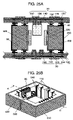
BRIEF DESCRIPTION OF THE DRAWINGS
FIG. 1A is a cross sectional view of a stereoscopic electronic circuit device according to a first embodiment of the present invention.
FIG. 1B is a perspective view of a relay board of the stereoscopic electronic circuit device according to the first embodiment of the present invention.
FIG. 2A is a cross sectional view of a first modified example of the stereoscopic electronic circuit device according to the first embodiment of the present invention.
FIG. 2B is a perspective view of a relay board of the first modified example of the stereoscopic electronic circuit device according to the first embodiment of the present invention.
FIG. 3A is a cross sectional view of a second modified example of the stereoscopic electronic circuit device according to the first embodiment of the present invention.
FIG. 3B is a perspective view of a relay board of the second modified example of the stereoscopic electronic circuit device according to the first embodiment of the present invention.
FIG. 4A is a cross sectional view of a third modified example of the stereoscopic electronic circuit device according to the first embodiment of the present invention.
FIG. 4B is a perspective view of a relay board before molding of the third modified example of the stereoscopic electronic circuit device according to the first embodiment of the present invention.
FIG. 4C is a perspective view of the relay board after molding of the third modified example of the stereoscopic electronic circuit device according to the first embodiment of the present invention.
FIG. 5A is a cross sectional view of a stereoscopic electronic circuit device according to a second embodiment of the present invention.
FIG. 5B is a perspective view of a relay board of the stereoscopic electronic circuit device according to the second embodiment of the present invention.
FIG. 6A is a cross sectional view of a first modified example of the stereoscopic electronic circuit device according to the second embodiment of the present invention.
FIG. 6B is a perspective view of a relay board of the first modified example of the stereoscopic electronic circuit device according to the second embodiment of the present invention.
FIG. 7A is a cross sectional view of a second modified example of the stereoscopic electronic circuit device according to the second embodiment of the present invention.
FIG. 7B is a perspective view of a relay board before molding of the second modified example of the stereoscopic electronic circuit device according to the second embodiment of the present invention.
FIG. 7C is a perspective view of the relay board after molding of the second modified example of the stereoscopic electronic circuit device according to the second embodiment of the present invention.
FIGS. 8A, 8B are perspective views of a relay board of a third modified example of the stereoscopic electronic circuit device according to the second embodiment of the present invention.
FIG. 9A is a cross sectional view of a fourth modified example of the stereoscopic electronic circuit device according to the second embodiment of the present invention.
FIG. 9B is a perspective view of a relay board of the fourth modified example of the stereoscopic electronic circuit device according to the second embodiment of the present invention.
FIGS. 10A, 10B are perspective views of a relay board of a fifth modified example of the stereoscopic electronic circuit device according to the second embodiment of the present invention.
FIG. 11A is a cross sectional view of a stereoscopic electronic circuit device according to a third embodiment of the present invention.
FIG. 11B is a perspective view of a relay board of the stereoscopic electronic circuit device according to the third embodiment of the present invention.
FIGS. 12A and 12B are perspective views of a relay board of a first modified example of the stereoscopic electronic circuit device according to the third embodiment of the present invention.
FIG. 13A is a cross sectional view of a second modified example of the stereoscopic electronic circuit device according to the third embodiment of the present invention.
FIG. 13B is a perspective view of a relay board of the second modified example of the stereoscopic electronic circuit device according to the third embodiment of the present invention.
FIG. 14A is a cross sectional view of a stereoscopic electronic circuit device according to a fourth embodiment of the present invention.
FIG. 14B is a perspective view of a relay board of the stereoscopic electronic circuit device according to the fourth embodiment of the present invention.
FIG. 15A is a cross sectional view of a first modified example of the stereoscopic electronic circuit device according to the fourth embodiment of the present invention.
FIG. 15B is a perspective view of a relay board of the first modified example of the stereoscopic electronic circuit device according to the fourth embodiment of the present invention.
FIG. 16A is a cross sectional view of a second modified example of the stereoscopic electronic circuit device according to the fourth embodiment of the present invention.
FIG. 16B is a perspective view of a relay board of the second modified example of the stereoscopic electronic circuit device according to the fourth embodiment of the present invention.
FIG. 17A is a cross sectional view of a third modified example of the stereoscopic electronic circuit device according to the fourth embodiment of the present invention.
FIG. 17B is a perspective view of a relay board of the third modified example of the stereoscopic electronic circuit device according to the fourth embodiment of the present invention.
FIG. 18A is a cross sectional view of a stereoscopic electronic circuit device according to a fifth embodiment of the present invention.
FIG. 18B is a perspective view of a relay board of the stereoscopic electronic circuit device according to the fifth embodiment of the present invention.
FIG. 19A is a cross sectional view of a first modified example of the stereoscopic electronic circuit device according to the fifth embodiment of the present invention.
FIG. 19B is a perspective view of a relay board of the first modified example of the stereoscopic electronic circuit device according to the fifth embodiment of the present invention.
FIG. 20A is a cross sectional view of a second modified example of the stereoscopic electronic circuit device according to the fifth embodiment of the present invention.
FIG. 20B is a perspective view of a relay board of the second modified example of the stereoscopic electronic circuit device according to the fifth embodiment of the present invention.
FIG. 21 is a cross sectional view of a stereoscopic electronic circuit device according to a sixth embodiment of the present invention.
FIG. 22A is a cross sectional view of a modified example of the stereoscopic electronic circuit device according to the sixth embodiment of the present invention.
FIG. 22B is a perspective view of a relay board of the modified example of the stereoscopic electronic circuit device according to the sixth embodiment of the present invention.
FIG. 23 is a cross sectional view of a stereoscopic electronic circuit device according to a seventh embodiment of the present invention.
FIG. 24A is a cross sectional view of a first modified example of the stereoscopic electronic circuit device according to the seventh embodiment of the present invention.
FIG. 24B is a perspective view of a relay board of the first modified example of the stereoscopic electronic circuit device according to the seventh embodiment of the present invention.
FIG. 25A is a cross sectional view of a second modified example of the stereoscopic electronic circuit device according to the seventh embodiment of the present invention.
FIG. 25B is a perspective view of a relay board of the second modified example of the stereoscopic electronic circuit device according to the seventh embodiment of the present invention.
FIG. 26A is a cross sectional view of a third modified example of the stereoscopic electronic circuit device according to the seventh embodiment of the present invention.
FIG. 26B is a perspective view of a relay board of the third modified example of the stereoscopic electronic circuit device according to the seventh embodiment of the present invention.
FIG. 27 is a cross sectional view of a fourth modified example of the stereoscopic electronic circuit device according to the seventh embodiment of the present invention.
FIG. 28A is a cross sectional view of a stereoscopic electronic circuit device according to an eighth embodiment of the present invention.
FIG. 28B is a perspective view of a relay board of the stereoscopic electronic circuit device according to the eighth embodiment of the present invention.
FIG. 29A is a perspective view of a modified example of the stereoscopic electronic circuit device according to the eighth embodiment of the present invention.
FIG. 29B is a perspective view of a relay board of the modified example of the stereoscopic electronic circuit device according to the eighth embodiment of the present invention.
FIG. 30 is a cross sectional view of a conventional electronic circuit device.
FIG. 31 is a cross sectional view of another conventional electronic circuit device.
FIG. 32 is a cross sectional view of further another conventional electronic circuit device.
DETAILED DESCRIPTION OF THE INVENTION
The following is a description of embodiments of the present invention with reference to accompanying drawings. Equivalent components will be referred to with the same marks and will not be repeatedly described in detail. Each component is exaggerated for purposes of illustration.
First Embodiment
FIGS. 1A and 1B show the structure of a stereoscopic electronic circuit device according to a first embodiment of the present invention. FIG. 1A is a cross sectional view taken along the line A-A′ of FIG. 1B, and FIG. 1B is a perspective view of relay board 10 shown in FIG. 1A.
The stereoscopic electronic circuit device has a three-dimensional connection structure in which first circuit board 20 and second circuit board 30 are connected with each other electrically and mechanically via relay board 10 disposed therebetween by using connection members 40. First circuit board 20 may be a part of an interconnection board to be connected with another circuit board. Second circuit board 30 may be a part of what is called a mother board. In short, relay board 10 has the function of connecting first circuit board 20 and second circuit board 30. Connection members 40 can be solder balls, micro connectors, heat seal connectors, anisotropic conductive films, soldering bumps or other kinds of bumps. Relay board 10 is bonded with pressure to first circuit board 20 and second circuit board 30 via connection members 40.
As shown in FIG. 1B, relay board 10 has recesses 50. Recesses 50 are mounted with electronic components 60 and are provided with lead-out wirings 70 extending from electronic components 60. The term “recesses” used here is not limited to the ones formed inside surfaces (recesses 50 in FIG. 1A) but includes concaves extending outside the surfaces (recesses 460 in FIG. 16B), which will be described later.
Relay board 10 also has land parts 90 for connecting between lead-out wirings 70 and first circuit board 20 or second circuit board 30 on its opposing surfaces that face first circuit board 20 or second circuit board 30 (hereinafter referred to as opposing surfaces 80). Hereinafter, the term opposing surfaces 80 do not include the recesses formed therein, unless otherwise noted.
Relay board 10 also has board interconnections 100 for connecting between first circuit board 20 and second circuit board 30 on its sides different from opposing surfaces 80 having land parts 90 thereon. Board interconnections 100 are connected with board connection lands 110 formed on opposing surfaces 80.
First circuit board 20 and second circuit board 30 are each formed of electrodes 120, conductive via holes (hereinafter referred to as via hole) 130 and insulating members 140. Alternatively, these boards can be a double side printed wiring board or a multilayer printed wiring board mounted with other electronic components 150 and 160. The electrodes of electronic components 60 and other electronic components 150 and 160 are electrically connected with the corresponding electrodes via connection members 170 such as solder or conductive adhesive. Electronic components 60, and other electric components 150 and 160 are general passive components such as semiconductor elements including ICs and LSIs, resistors, capacitors and inductors. Alternatively, it is possible to mount bare chip electronic components by flip chip mounting or wire bonding connection.
First circuit board 20 and second circuit board 30 can be made of general resin or inorganic boards. Particularly preferable are glass epoxy substrates, aramid substrates, build-up substrates, glass ceramic substrates, alumina substrates and the like. Relay board 10 is made of general thermoplastic or thermosetting resin. Thermoplastic resin allows relay board 10 to be molded into a desired shape by injection molding or another process. Thermosetting resin enables relay board 10 to be formed into a desired shape by cutting work. Preferable thermoplastic resins include: PPA (polyphthalamide), PPS (polyethylene sulfide), PBT (polybutylene terephthalate), ester-based resin and LCP (liquid crystal polymer). Preferable thermosetting resins include normal epoxy resins. In a case where relay board 10 is made of resin with a small Young's modulus, relay board 10 can reduce the stress caused by the difference in thermal expansion coefficient between first circuit board 20 and second circuit board 30.
The stereoscopic interconnections including lead-out wirings 70 of relay board 10 are formed either by a printing process with conductive paste, by applying metal foil or depositing a plated layer onto the board surface and then applying a laser process or by another method. The stereoscopic interconnections can be made from Ag, Sn, Zn, Pd, Bi, Ni, Au, Cu, C, Pt, Fe, Ti or Pb and so on.
The aforementioned stereoscopic electronic circuit device with the three-dimensional connection structure allows relay board 10 to mount electronic components 60 thereon, thereby achieving high density mounting, while securing the area for connecting between the circuit boards. Furthermore, other electronic components 150 and 160 mounted on first circuit board 20 and second circuit board 30 can be connected with electronic components 60 mounted on relay board 10 in the shortest distance so as to improve the high-frequency properties of the stereoscopic electronic circuit device, thereby achieving high-speed operation of the electronic device using the electronic circuit.
It is also possible to connect first circuit board 20 and second circuit board 30 via board connection lands 110 by providing via holes (not illustrated) penetrating opposing surfaces 80 of relay board 10. It is also possible to connect between electronic components 60 in recesses 50 of relay board 10 by providing via holes penetrating recesses 50 and then connecting the via holes with lead-out wirings 70 and the like. If it is unnecessary to connect first circuit board 20 and second circuit board 30 with each other, there is no need for providing board interconnections 100, via holes or board connection lands 110.
First circuit board 20 can be made up exclusively of an interconnection board, without mounting other electronic component 150.
In order to secure the connection strength and reliability, electronic components 60, other electronic components 150, 160 and recesses 50 may be molded out of molding resin.
It is also possible to mount a plurality of electronic components on one recess 50.
FIGS. 2A and 2B show the structure of the stereoscopic electronic circuit device according to a first modified example of the first embodiment of the present invention. FIG. 2A is a cross sectional view taken along the line A-A′ of FIG. 2B, and FIG. 2B is a perspective view of relay board 10 shown in FIG. 2A.
In FIGS. 2A and 2B, a side surface of relay board 10 is mounted with electronic component 180. In this structure, any electronic component smaller in size than the side surface can be mounted thereon. Chip capacitors and chip resistors in particular can be suitably mounted.
FIGS. 3A and 3B show the structure of the stereoscopic electronic circuit device according to a second modified example of the first embodiment of the present invention. FIG. 3A is a cross sectional view taken along the line A-A′ of FIG. 3B, and FIG. 3B is a perspective view of relay board 10 shown in FIG. 3A. In this structure, electronic components 60 shaped like thin plates or chips are stacked in one of recesses 50 of relay board 10.
FIGS. 4A-4C show the structure of the stereoscopic electronic circuit device according to a third modified example of the first embodiment of the present invention. FIG. 4A is a cross sectional view taken along the line A-A′ of FIG. 4B, and FIGS. 4B and 4C are perspective views of relay board 210 of FIG. 4A before and after being sealed using molding resin 190. When through-hole 200 is formed between recesses 50 of relay board 210 and then electronic components 60 are resin-molded, recess 50 on the bottom side is nearly entirely filled with molding resin 190. This structure improves not only the bonding strength between relay board 210 and second circuit board 30 but also the reliability of electronic components 60 sealed using molding resin 190.
Second Embodiment
FIGS. 5A and 5B show the structure of a stereoscopic electronic circuit device according to a second embodiment of the present invention. FIG. 5A is a cross sectional view taken along the line A-A′ of FIG. 5B, and FIG. 5B is a perspective view of relay board 10 shown in FIG. 5A.
Similar to that of the first embodiment, this stereoscopic electronic circuit device has a three-dimensional connection structure in which first circuit board 20 and second circuit board 30 are connected with each other electrically and mechanically via relay board 10 disposed therebetween by using connection members 40.
As shown in FIG. 5B, relay board 10 has recesses 50. Recesses 50 are mounted with electronic components 60 and are provided with lead-out wirings 70 extending from electronic components 60. Relay board 10 also has land parts 90 which are connected with lead-out wirings 70, and which connect between lead-out wirings 70 and first circuit board 20 or second circuit board 30 on opposing surfaces 80 that face first circuit board 20 or second circuit board 30.
It is also possible, when necessary, to provide board connection lands 110 for connecting between first circuit board 20 and second circuit board 30 onto opposing surfaces 80 or recesses 50 of relay board 10 through via holes 220 penetrating in the direction towards opposing surfaces 80. Furthermore, at least part of and preferably the whole of the outer surface of relay board 10 is covered with third shield conductor 250. First circuit board 20 is formed of electrodes 120, via holes 130, first shield conductor 230 and insulating members 140. When necessary, first circuit board 20 may be mounted with other electronic component 150 so as to make a double side or multilayer printed wiring board. Similarly, second circuit board 30 is formed of electrodes 120, via holes 130, second shield conductor 240 and insulating members 140. When necessary, second circuit board 30 may be mounted with other electronic component 160 so as to make a double sided or multilayer interconnection board. First shield conductor 230 of first circuit board 20 and second shield conductor 240 of second circuit board 30 are provided throughout, except for the regions of via holes 130. Via holes 130, if they are ground electrodes, may be connected with first shield conductor 230 or second shield conductor 240. The electrodes of electronic components 60 and other electronic components 150 and 160 are electrically connected with the corresponding electrodes via connection members 170 such as solder or conductive adhesive.
In the aforementioned stereoscopic electronic circuit device with the three-dimensional connection structure, first shield conductor 230 of first circuit board 20, second shield conductor 240 of second circuit board 30 and third shield conductor 250 provided on the outer surface of relay board 10 can be connected with each other to shield radiation noise coming from an external electronic device or going out of the stereoscopic electronic circuit device.
Specifically, first of all, electronic component 150 on first circuit board 20 and electronic component 160 on second circuit board 30 are connected with each other inside relay board 10. At the same time, first shield conductor 230 of first circuit board 20 and second shield conductor 240 of second circuit board 30 are connected with each other via third shield conductor 250 provided on the outer surface of relay board 10. This structure can completely separate the electronic components mounted inside relay board 10 from outside, thereby obtaining a high shielding effect. The gaps between via holes 130 and first shield conductor 230 or second shield conductor 240 are preferably not more than ½ of the frequency to be used. However, the gap size is not limited to this, and can be designed in accordance with radiation power or the anti-noise performance of the electronic components.
As shown in a first modified example of the stereoscopic electronic circuit device shown in FIGS. 6A and 6B, electronic components 60 and recesses 50 can be resin-shielded by using insulating molding resin 190 to stabilize connection strength and to improve reliability including moisture resistance.
FIGS. 7A-7C show the structure of a stereoscopic electronic circuit device according to a second modified example of the second embodiment of the present invention.
FIG. 7A is a cross sectional view of the stereoscopic electronic circuit device taken along the line A-A′ of FIG. 7C. FIGS. 7B and 7C are perspective views of relay board 260 before and after being resin-shielded using molding resin 190, respectively. Recesses 50 of relay board 260 are provided with throughholes 200, so that when electronic components 60 are resin-shielded using molding resin 190, recesses 50 can be nearly fully filled with molding resin 190. This structure improves the bonding strength between relay board 260 and second circuit board 30, thereby stabilizing the connection strength between the electrodes. The resin-shielding of electronic components 60 using molding resin 190 also improves reliability including moisture resistance.
FIGS. 8A and 8B are perspective views of a relay board of a third modified example of the second embodiment of the present invention.
A plurality of electronic components 60 may be laid on one recess 50 as shown in FIG. 8A, or be stacked one on top of another as shown in FIG. 8B. Either can achieve much higher density mounting.
FIGS. 9A and 9B show the structure of a stereoscopic electronic circuit device according to a fourth modified example of the second embodiment of the present invention. FIG. 9A is a cross sectional view taken along the line A-A′ of FIG. 9B, and FIG. 9B is a perspective view of relay board 10 shown in FIG. 9A. Relay board 10 is provided, on its side surface, with shield electrodes 270 having an electromagnetic shielding effect. Shield electrodes 270 are formed by extending ground interconnections out of lead-out wirings 70 extending from electronic components 60 to the side surface. Alternatively, shield electrodes 270 may be formed by bundling ground interconnections out of board interconnections 100 for connecting first circuit board 20 and second circuit board 30.
As shown in this structure, a simple structure of providing shield electrodes 270 exclusively on specific region can reduce spurious radiation from electronic components 60 or prevent the occurrence of circuit malfunction due to external noise.
FIGS. 10A and 10B show a relay board according to a fifth modified example of the second embodiment of the present invention. As shown in the perspective views of FIGS. 10A and 10B, of lead-out wirings 70, wirings leading to the ground are formed on a side surface as shield electrodes 280 having a flat shape. This structure can improve the effect of reducing the spurious radiation from electronic components 60 and the like.
Third Embodiment
FIGS. 11A and 11B show the structure of a stereoscopic electronic circuit device according to a third embodiment of the present invention. FIG. 11A is a cross sectional view taken along the line A-A′ of FIG. 11B, and FIG. 11B is a perspective view of relay board 260 shown in FIG. 11A.
In FIG. 11A, relay board 260 has, on its side surface other than opposed surfaces 80, recess 290 on which to mount electronic component 60. The side surface is provided with lead-out wirings 70 extending from electronic component 60, and with board interconnections 100 for connecting first circuit board 20 and second circuit board 30. Opposing surfaces 80 of relay board 260 are provided with land parts 90 to be connected to lead-out wirings 70, and also provided with board connection lands 110 to be connected to board interconnections 100. Relay board 26 has another side surface having another recess 300 formed thereon which is mounted with electronic component 310 and which is molded using molding resin 190. The surface of molding resin 190 is smoothed and is provided with shield electrodes 320 thereon to be connected with ground electrodes.
This structure can shield electronic component 310 and others which cause noise or are vulnerable to external noise by separating them from electronic component 60 and the like, thereby improving reliability. The structure of relay board 260 can not only connect between first circuit board 20 and second circuit board 30, but also mount electronic components 60 and 310 on side surfaces.
Although in FIGS. 11A, 11B both first circuit board 20 and second circuit board 30 are multilayer circuit boards provided with electrodes 120, via holes 130 and insulating members 140, they may be double sided circuit boards instead.
FIGS. 12A and 12B show a relay board of a first modified example of the third embodiment of the present invention.
As shown in the perspective view of the relay board in FIG. 12A, side-surface interconnections 330 for connecting between the ground electrodes of board interconnections 100 on one side surface and the corresponding ground electrodes of board interconnections 100 on the opposite side surface of the relay board are formed on opposing surfaces 80. With this structure, the interconnections connected with a plurality of ground electrodes are connected with each other to strengthen the ground, thereby shielding electric noise. Alternatively, as shown in the perspective view of the relay board shown in FIG. 12B, the ground electrodes can be strengthened by providing shield electrodes 340 having a flat shape on opposing surfaces 80 of the relay board.
FIGS. 13A and 13B show the structure of a stereoscopic electronic circuit device according to a second modified example of the third embodiment of the present invention.
As shown in FIGS. 13A and 13B, recesses 350 on which to mount electronic components 360 are formed on side surfaces other than opposing surfaces 80 of relay board 370, and third shield conductor 250 is provided on the entire surface, except for the region of land parts 380 formed on opposing surfaces 80 of relay board 370. This structure secures the protection of electronic component 360 vulnerable to noise and the like.
Fourth Embodiment
FIGS. 14A and 14B show the structure of a stereoscopic electronic circuit device according to a fourth embodiment of the present invention. FIG. 14A is a cross sectional view taken along the line A-A′ of FIG. 14B, and FIG. 14B is a perspective view of relay board 390 shown in FIG. 14A.
This stereoscopic electronic circuit device has a three-dimensional connection structure in which first circuit board 20 and second circuit board 30 are connected with each other electrically and mechanically via relay board 390 disposed therebetween by using connection members 40. Relay board 390 has recesses on opposing surfaces 80 and on side surfaces so as to mount electronic components 60 and 400, respectively, thereon. In addition, opposing surfaces 80 of relay board 390 are provided with land parts 90A to be connected with lead-out wirings 70 extending from electronic components 60; land parts 90B to be connected with lead-out wirings 410 extending from electronic components 400 mounted on the side surfaces; and board connection lands 110 for connecting between first circuit board 20 and second circuit board 30.
The aforementioned stereoscopic electronic circuit device can mount other electronic component 150 and 160 on first circuit board 20 and second circuit board 30, and at the same time, mount electronic components 60 and 400 on recesses 50 of relay board 390, thereby achieving higher density mounting.
FIGS. 15A and 15B show the structure of a stereoscopic electronic circuit device according to a first modified example of the fourth embodiment of the present invention.
FIG. 15A is a cross sectional view of the stereoscopic electronic circuit device taken along the line A-A′ of FIG. 15B. FIG. 15B is a perspective view of a relay board of FIG. 15A before a recess is resin-shielded using molding resin.
As shown in FIG. 15A, in the direction towards opposing surfaces 80 of relay board 370, via holes 430 are formed so as to connect between lead-out wirings 420 extending from electronic component 360 and land parts 380 formed on opposing surfaces 80 of relay board 370, and other via holes 430 are formed to connect between board connection lands 110 for connecting between first circuit board 20 and second circuit board 30. Later, recess 350 of relay board 370 shown in FIG. 15B is filled with molding resin 190. After the surface of molding resin 190 is smoothed, the outer surface of relay board 370 including the smoothed surface is covered with third shield conductor 250.
In this structure, first shield conductor 230 of first circuit board 20, second shield conductor 240 of second circuit board 30 and third shield conductor 250 provided on the outer surface of relay board 370 can be connected with each other to shield radiation noise coming from an external electronic device or going out of the stereoscopic electronic circuit device.
FIGS. 16A and 16B show the structure of a stereoscopic electronic circuit device according to a second modified example of the fourth embodiment of the present invention.
FIG. 16A is a cross sectional view of the stereoscopic electronic circuit device taken along the line A-A′ of FIG. 16B. FIG. 16B is a perspective view of a relay board of FIG. 16A before a recess is resin-shielded using molding resin.
As shown in FIG. 16B, lead-out wirings 450 extending from electronic components 440, and board interconnections 470 for connecting between first circuit board 20 and second circuit board 30 are formed in recesses 460, and are connected with land parts 90 or board connection lands 110 formed on opposing surfaces 80. Later, recesses 460 of relay board 390 shown in FIG. 16B are filled with molding resin 190. After the surface of molding resin 190 is made to conform to the shape of opposing surfaces 80 of relay board 390, the outer surface of relay board 390 is covered with third shield conductor 250.
First circuit board 20 and second circuit board 30 may be connected with each other through via holes (not illustrated) of relay board 390 without using board interconnections 470, or may be connected through both board interconnections 470 and the via holes.
This structure allows recesses 460 to be mounted with electronic components 440 whose length is nearly equal to the height of relay board 390.
FIGS. 17A and 17B show the structure of a stereoscopic electronic circuit device according to a third modified example of the fourth embodiment of the present invention.
As shown in FIGS. 17A and 17B, relay board 13 is provided, on all its outer side surfaces except for opposing surfaces 80, with recesses 460 extending to opposing surfaces 80 so as to mount electronic components 440 thereon. This structure can further improve mounting density.
Fifth Embodiment
FIGS. 18A and 18B show the structure of a stereoscopic electronic circuit device according to a fifth embodiment of the present invention. FIG. 18A is a cross sectional view taken along the line A-A′ of FIG. 18B. In the present embodiment, relay board 10 used in the first embodiment is linked with another in such a manner as to be stacked one on top of the other. Each recess 50 is mounted with electronic component 60.
Opposing surfaces 80 of each relay board 10 are provided with land parts 90 for connecting between lead-out wirings 70 extending from electronic components 60 and first circuit board 20 or second circuit board 30, and are also provided with connection terminals for connecting between relay boards 10.
FIG. 18B is a perspective view of relay boards 10 linked with each other. Each relay board 10 is provided, on opposing surfaces 80, with land parts 90 for connecting between lead-out wirings 70 extending from electronic components 60 and first circuit board 20 or second circuit board 30, and also provided with board connection lands 110 for connecting between first circuit board 20 and second circuit board 30 via board interconnections 100. As shown in FIG. 18A, connection terminals 480 are linked with each other by making one side of each of opposing surfaces 80 have unevenness and engaging the uneven sides with each other. Besides such engagement, relay boards 10 can also be solder-bonded. Alternatively, the electrodes can be bonded with pressure or with conductive resin.
In the present embodiment, two relay boards 10 are stacked one on top of the other; however, a larger number of relay boards 10 can be stacked when necessary. It is also possible to link relay boards two dimensionally or to be distanced from each other. These structures achieve more stable connection between first circuit board 20 and second circuit board 30.
With the aforementioned structure, first circuit board 20 and second circuit board 30 are connected with each other via a plurality of relay boards 10. The mounting of electronic components 60 onto recesses 50 in a multilayer can achieve higher density mounting.
FIGS. 19A and 19B show the structure of a stereoscopic electronic circuit device according to a first modified example of the fifth embodiment of the present invention. FIG. 19A is a cross sectional view of the stereoscopic electronic circuit device taken along the line A-A′ of FIG. 19B. FIG. 19B is a perspective view of relay board 10 shown in FIG. 19A. This stereoscopic electronic circuit device is achieved by providing first circuit board 20 with first shield conductor 230, second circuit board 30 with second shield conductor 240, and relay board 10 with third shield conductor 250 in the stereoscopic electronic circuit device according to the fifth embodiment.
As shown in FIG. 19B, opposing surfaces 80 or recesses 50 of relay boards 10 are provided with board connection lands 110 for connecting between first circuit board 20 and second circuit board 30 through via holes 220 penetrating in the direction towards opposing surfaces 80. Via holes 220 thus formed in relay boards 10 may be omitted when unnecessary.
With the aforementioned structure, first shield conductor 230 of first circuit board 20, second shield conductor 240 of second circuit board 30 and third shield conductor 250 provided on the outer surfaces of relay boards 10 are connected with each other to shield radiation noise coming from an external electronic device or going out of the stereoscopic electronic circuit device.
FIGS. 20A and 20B show the structure of a stereoscopic electronic circuit device according to a second modified example of the fifth embodiment of the present invention.
As shown in FIGS. 20A and 20B, the stereoscopic electronic circuit device is structured by linking a plurality of relay boards two dimensionally or distanced from each other. This structure expands the connection area (opposing surfaces 80), thereby further stabilizing the connection between first circuit board 20 and second circuit board 30.
Sixth Embodiment
FIG. 21 is a cross sectional view of a stereoscopic electronic circuit device according to a sixth embodiment of the present invention. First circuit board 20 and second circuit board 30 are connected with each other electrically and mechanically via relay board 10 disposed therebetween by using connection members 40. Recesses 50 formed on opposing surfaces 80 of relay board 10 are mounted with electronic components 60 using connection members 40. Opposing surfaces 80 are provided with land parts 90 to be connected with lead-out wirings 70 extending from electronic components 60, and also provided with board interconnections lands (not illustrated) for connecting between first circuit board 20 and second circuit board 30. Electronic components 60 mounted on recesses 50 of relay board 10, and other electronic components 150 and 160 which are mounted respectively on the surfaces of first circuit board 20 and second circuit board 30 that face opposing surfaces 80 of relay board 17 are placed so as not to be overlapped with each other when projected in the thickness or height direction.
This structure can reduce the height or thickness of the stereoscopic electronic circuit device.
In addition, connecting first circuit board 20 and second circuit board 30, and mounting electronic components 60 on relay board 10 stereoscopically can achieve the low profile of the stereoscopic electronic circuit device and high density mounting at the same time.
FIGS. 22A and 22B show the structure of a stereoscopic electronic circuit device according to a modified example of the sixth embodiment of the present invention.
FIG. 22A is a cross sectional view of the stereoscopic electronic circuit device taken along the line A-A′ of FIG. 22B. FIG. 22B is a perspective view of relay board 10 shown in FIG. 22A.
This stereoscopic electronic circuit device is achieved by providing first circuit board 20 with first shield conductor 230, second circuit board 30 with second shield conductor 240, and relay board 10 with third shield conductor 250 in the stereoscopic electronic circuit device according to the sixth embodiment.
As shown in FIG. 22A, opposing surfaces 80 of relay board 10 have electronic components 60 mounted onto recesses 50 via connection members 170, and also have land parts 90 to be connected with lead-out wirings 70 extending from electronic components 60 in the vicinity of the end parts of opposing surfaces 80. When necessary, relay board 10 can have board connection lands 110 for connecting first circuit board 20 and second circuit board 30 through via holes 220 penetrating opposing surfaces 80 or recesses 50 in the direction towards opposing surfaces 80.
With the aforementioned structure, first shield conductor 230 of first circuit board 20, second shield conductor 240 of second circuit board 30 and third shield conductor 250 provided on the outer surface of relay board 10 are connected with each other to shield radiation noise coming from an external electronic device or going out of the stereoscopic electronic circuit device.
Seventh Embodiment
FIG. 23 is a cross sectional view of a stereoscopic electronic circuit device according to a seventh embodiment of the present invention.
This stereoscopic electronic circuit device has a structure in which first circuit board 20 and second circuit board 30 are connected with each other electrically and mechanically via relay frame 490 disposed therebetween by using connection members 40.
Relay frame 490 has via holes 500 for connecting between first circuit board 20 and second circuit board 30. The inner surface of relay frame 490 is mounted with chip electronic components 60, and the outer surface is covered with conductive shield layer 510 for noise prevention. The electrodes of first circuit board 20 and the electrodes of second circuit board 30 are connected with each other electrically and mechanically through connection members 40, and via holes 500.
The electrodes of electronic components 60 mounted on the inner surface of relay frame 490 are connected with the electrodes of first circuit board 20 or second circuit board 30 at the land parts (not illustrated) connected with lead-out wirings (not illustrated) via connection members 40.
The height of relay frame 490 is designed to be larger than the sum of the height of other electronic components 150 and 160 mounted on the surfaces of first circuit board 20 and second circuit board 30 that face the opposing surfaces of relay frame 490 (hereinafter referred to as opposing surfaces 80) and the height of connection members 170.
In this structure, relay frame 490 not only functions as a spacer but also improves mounting density by mounting electronic components 60 on its inner surfaces. Furthermore, other electronic components 150 and 160 respectively mounted on first circuit board 20 and second circuit board 30 can be connected with electronic components 60 mounted on relay frame 490 in the shortest distance so as to improve the high-frequency properties of the stereoscopic electronic circuit device, thereby achieving high-speed operation of the electronic device.
FIGS. 24A and 24B show the structure of a stereoscopic electronic circuit device according to a first modified example of the seventh embodiment of the present invention.
FIG. 24A is a cross sectional view of the stereoscopic electronic circuit device taken along the line A-A′ of FIG. 24B. FIG. 24B is a perspective view of relay frame 490 shown in FIG. 24A.
This stereoscopic electronic circuit device is achieved by connecting between first circuit board 20 provided with first shield conductor 230 and second circuit board 30 provided with second shield conductor 240 electrically and mechanically via relay frame 490 provided with third shield conductor 250 and disposed therebetween by using connection members 40 in the stereoscopic electronic circuit device according to the seventh embodiment.
As shown in FIG. 24A, the inner surface of relay frame 490 is mounted with electronic components 520, and is provided with lead-out wirings 530 extending from electronic components 520, and board interconnections 540 for connecting between first circuit board 20 and second circuit boards 30. Opposing surfaces 80 of relay frame 490 that face first circuit board 20 or second circuit board 30 are provided with land parts 90 connected to lead-out wirings 530, and board connection lands 110 connected to board interconnections 540. Consequently, first circuit board 20, second circuit board 30 and electronic components 520 are electrically connected with each other via connection members 40. When necessary, it is possible to connect board connection lands 110 with first circuit board 20 and second circuit board 30 through via holes (not illustrated) penetrating opposing surfaces 80 of relay frame 490.
This structure can reduce the projected area of the stereoscopic electronic circuit device since electronic components 520 can be disposed vertically. In addition, when other electronic component 550 with a large height is mounted on first circuit board 20 or second circuit board 30, it is unnecessary to increase the height of relay frame 490. Furthermore, it is possible to mount electronic components 520 having a height nearly equal to the height of relay frame 490, indicating the effective mounting of a large-sized electronic component.
FIGS. 25A and 25B show the structure of a stereoscopic electronic circuit device according to a second modified example of the seventh embodiment of the present invention.
As shown in FIG. 25B, it is also possible to assemble the stereoscopic electronic circuit device shown in FIG. 25A by dividing relay frame 490 at least into two parts, and then mounting electronic components 520.
This structure facilitates the mounting of electronic components 520 onto the inner surface of relay frame 490, and the formation of lead-out wirings 530.
FIGS. 26A and 26B show the structure of a stereoscopic electronic circuit device according to a third modified example of the seventh embodiment of the present invention.
As shown in FIGS. 26A and 26B, recesses 560 are formed on the outer surfaces of relay frame 490 in such a manner as to extend to opposing surfaces 80, and electronic components 520 are mounted on recesses 560. Later, recesses 560 are molded using molding resin 190, and then third shield conductor 250 is formed, thereby completing the stereoscopic electronic circuit device. This structure can achieve higher density mounting.
FIG. 27 shows the structure of a stereoscopic electronic circuit device according to a fourth modified example of the seventh embodiment of the present invention.
As shown in FIG. 27, this stereoscopic electronic circuit device is achieved by providing the stereoscopic electronic circuit device according to the seventh embodiment with inductors or loop antennas made by helixes on the outer surface of relay frame 490. In general, the formation of inductors or loop antennas requires large space. To overcome this problem, relay frame 490 is utilized as a bobbin for wound inductors or loop antennas so as to miniaturize the stereoscopic electronic circuit device.
The helixes can be replaced by inductors or loop antennas 570 made by forming a metal film on a side surface of relay frame 490, and then patterning the film into a coil.
The aforementioned structure enables the stereoscopic electronic circuit device to be mounted with IC chips for transmitting and receiving information by radio, that is, IC tags.
It is also possible to make relay frame 490 from resin capable of injection molding so as to facilitate the formation of bar-like trenches for helixes on the outer surface.
Eighth Embodiment
FIGS. 28A and 28B show the structure of a stereoscopic electronic circuit device according to an eighth embodiment of the present invention.
FIG. 28A is a cross sectional view of the stereoscopic electronic circuit device taken along the line A-A′ of FIG. 28B. FIG. 28B is a perspective view of relay board 370 shown in FIG. 28A.
The stereoscopic electronic circuit device has a structure in which first circuit board 20 and second circuit board 30 are disposed, e.g. in the shape of a letter L, and relayed by relay board 370. This structure allows first circuit board 20 and second circuit board 30 to be connected with each other electrically and mechanically in an arbitrary direction.
FIGS. 29A and 29B show the structure of a stereoscopic electronic circuit device according to a modified example of the eighth embodiment of the present invention. FIG. 29A is a cross sectional view of the stereoscopic electronic circuit device taken along the line A-A′ of FIG. 29B. FIG. 29B is a perspective view of relay board 370 shown in FIG. 29A.
This stereoscopic electronic circuit device is achieved by providing first circuit board 20 with first shield conductor 230, second circuit board 30 with second shield conductor 240, and relay board 370 with third shield conductor 250 in the stereoscopic electronic circuit device according to the eighth embodiment. Third shield conductor 250 of relay board 370 is formed after recess 50, which is formed at least on a surface other than opposing surfaces 80 that face first circuit board 20 or second circuit board 30, is molded by using molding resin 190.
This structure allows first circuit board 20 and second circuit board 30 to be connected with each other in an arbitrary direction, and also provides a high shielding effect against electromagnetic waves.
It goes without saying that the aforementioned structure can be applied to a relay frame.
In the description in each of the aforementioned embodiments of the present invention, third shield conductor 250 on the outer surface of the relay board or the relay frame is extended to part of opposing surfaces 80 that face first circuit board 20 or second circuit board 30, thereby being connected with first circuit board 20 or second circuit board 30 there. However, when the connection with first circuit board 20 or second circuit board 30 is secured, third shield conductor 250 can be formed exclusively on the outer surface of the relay board or the relay frame, without causing any problem.

Claims (25)

1. A stereoscopic electronic circuit device, comprising:
a first circuit board;
a second circuit board;
a relay board provided between the first circuit board and the second circuit board, wherein
the relay board has a recess which is mounted with an electronic component and is provided with a lead-out wiring extending from the electronic component, and also has a land part for connecting the lead-out wiring with one of the first circuit board and the second circuit board on one of surfaces that face the first circuit board and the second circuit board;
the first circuit board and the second circuit board are connected with each other three-dimensionally via the land part of the relay board, and
at least a portion of an electrical component of at least one of the first or second circuit board is disposed within the recess of the relay board.
2. The stereoscopic electronic circuit device according to claim 1, wherein
at least one of the first circuit board and the second circuit board is mounted with an other electronic component.
3. The stereoscopic electronic circuit device according to claim 1, wherein
the recess of the relay board is formed on at least one of surfaces that face the first circuit board and the second circuit board, and the recess is mounted with the electronic component.
4. The stereoscopic electronic circuit device according to claim 1, wherein
the recess of the relay board is formed on a surface other than the surfaces that face the first circuit board and the second circuit board, and the recess is mounted with the electronic component.
5. The stereoscopic electronic circuit device according to claim 1, wherein
the recess of the relay board is formed on at least part of the surfaces that face the first circuit board and the second circuit board, and on at least part of a surface other than the surfaces that face the first circuit board and the second circuit board, and the electronic component is mounted on the recess.
6. The stereoscopic electronic circuit device according to claim 1, wherein
the recess of the rely board is mounted with a plurality of electronic components.
7. The stereoscopic electronic circuit device according to claim 1, wherein
an outer surface of the relay board has a shield electrode formed thereon.
8. The stereoscopic electronic circuit device according to claim 1, wherein
the first circuit board has a first shield conductor thereon, the second circuit board has a second shield conductor thereon, and the relay board has a third shield conductor on an outer surface thereof, and
the first shield conductor, the second shield conductor and the third shield conductor are connected with each other.
9. The stereoscopic electronic circuit device according to claim 1, wherein
the electronic component mounted on the recess of the relay board is resin-shield using molding resin.
10. The stereoscopic electronic circuit device according to claim 2, wherein
the electronic component mounted on the recess, and the other electronic component mounted on one of the first circuit board and the second circuit board are placed so as not to be overlapped with each other.
11. The stereoscopic electronic circuit device according to claim 1, wherein
the relay board has an inductor or a loop antenna on a side surface thereof.
12. The stereoscopic electronic circuit device according to claim 1, wherein
a plurality of relay boards are linked with each other so that the first circuit board and the second circuit board are connected with each other three-dimensionally.
13. The stereoscopic electronic circuit device according to claim 1, wherein
the relay board has a board interconnection on a side surface thereof, and also has a board connection land to be connected with the board interconnection on the surfaces that face the first circuit board and the second circuit board.
14. The stereoscopic electronic circuit device according to claim 13, wherein
the board interconnection is made up of a via hole penetrating the surfaces of the relay board that face the first circuit board and the second circuit board.
15. The stereoscopic electronic circuit device according to claim 1, wherein
at least one of the first circuit board and the second circuit board is a flexible circuit board.
16. A relay board, comprising:
a recess mounted with an electronic component and provided with a lead-out wiring extending from the electronic component; and
a land part for being connected with the lead-out wiring to be connected with an other circuit board on a surface of the relay board that faces the other circuit board,
wherein at least a portion of an electrical component of the other circuit board is disposed within the recess of the relay board.
17. The relay board according to claim 16, wherein
the recess of the relay board is formed on at least one surface that faces the other circuit board, and the recess is mounted with the electronic component.
18. The relay board according to claim 16, wherein
the recess of the relay board is formed on a surface other than the surface that faces the other circuit board, and the recess is mounted with the electronic component.
19. The relay board according to claim 16, wherein
the recess of the relay board is formed on at least part of the surface that faces the other circuit board, and at least part of a surface other than the surface that faces the other circuit board, and the electronic component is mounted on the recess.
20. The relay board according to claim 16, wherein
the recess of the rely board is mounted with a plurality of electronic components.
21. The relay board according to claim 16, wherein
a side surface of the relay board has one of a shield electrode and a third shield conductor formed thereon.
22. The relay board according to claim 16, wherein
the recess is resin-shield with molding resin.
23. The relay board according to claim 16, wherein
the relay board has a board interconnection on a side surface thereof, and also has a board connection land to be connected with the board interconnection on the surface of the relay board that faces the other circuit board.
24. The relay board according to claim 23, wherein
the board interconnection is made up of a via hole penetrating the surface of the relay board that faces the other circuit board.
25. The stereoscopic electronic circuit device according to claim 1, wherein the relay board includes:
an outer portion extending substantially orthogonal to and between the first and second circuit boards, and
a center portion extending substantially parallel to the first and second circuit boards,
wherein the recess which is mounted with the electronic component is on a first side of the center portion, and
another recess is mounted with another electrical component on a second side, opposite the first side.
US10/985,325 2004-02-02 2004-11-10 Stereoscopic electronic circuit device, and relay board and relay frame used therein Expired - Fee Related US7613010B2 (en)

Priority Applications (1)

Application Number Priority Date Filing Date Title
US12/562,444 US20100008056A1 (en) 2004-02-02 2009-09-18 Stereoscopic electronic circuit device, and relay board and relay frame used therein

Applications Claiming Priority (4)

Application Number Priority Date Filing Date Title
JP2004-025238 2004-02-02
JP2004025238A JP4046088B2 (en) 2004-02-02 2004-02-02 Three-dimensional electronic circuit device and its relay substrate and relay frame
JP2004058436A JP4186843B2 (en) 2004-03-03 2004-03-03 Three-dimensional electronic circuit device
JP2004-058436 2004-03-03

Related Child Applications (1)

Application Number Title Priority Date Filing Date
US12/562,444 Division US20100008056A1 (en) 2004-02-02 2009-09-18 Stereoscopic electronic circuit device, and relay board and relay frame used therein

Publications (2)

Publication Number Publication Date
US20050168961A1 US20050168961A1 (en) 2005-08-04
US7613010B2 true US7613010B2 (en) 2009-11-03

Family

ID=34810185

Family Applications (2)

Application Number Title Priority Date Filing Date
US10/985,325 Expired - Fee Related US7613010B2 (en) 2004-02-02 2004-11-10 Stereoscopic electronic circuit device, and relay board and relay frame used therein
US12/562,444 Abandoned US20100008056A1 (en) 2004-02-02 2009-09-18 Stereoscopic electronic circuit device, and relay board and relay frame used therein

Family Applications After (1)

Application Number Title Priority Date Filing Date
US12/562,444 Abandoned US20100008056A1 (en) 2004-02-02 2009-09-18 Stereoscopic electronic circuit device, and relay board and relay frame used therein

Country Status (2)

Country Link
US (2) US7613010B2 (en)
CN (1) CN100563405C (en)

Cited By (10)

* Cited by examiner, † Cited by third party
Publication number Priority date Publication date Assignee Title
US20090311884A1 (en) * 2006-09-22 2009-12-17 Panasonic Corporation Circuit device, circuit device manufacturing method and connecting member
US20090321898A1 (en) * 2008-06-25 2009-12-31 Reza Argenty Pagaila Conformal shielding integrated circuit package system
US20100265671A1 (en) * 2009-04-16 2010-10-21 Silitek Electronic (Guangzhou) Co., Ltd. Package structure of printed circuit board and package method thereof
US20110083894A1 (en) * 2007-09-04 2011-04-14 Stefan Kopf Electric circuit configuration having an mid circuit carrier and a connecting interface connected to it
US20130063415A1 (en) * 2011-09-09 2013-03-14 Qualcomm Mems Technologies, Inc. Backplate interconnect with integrated passives
US10420218B2 (en) * 2015-09-15 2019-09-17 Safran Electronics & Defense Compact electronic system and device comprising such a system
US20200137888A1 (en) * 2018-10-24 2020-04-30 Avary Holding (Shenzhen) Co., Limited. Printed circuit board and method for manufacturing the same
TWI737316B (en) * 2020-05-20 2021-08-21 大陸商鵬鼎控股(深圳)股份有限公司 Circuit board and method for manufacturing the same
US11189907B2 (en) * 2017-02-28 2021-11-30 Toyota Motor Europe Three-dimensional electronic circuit
US11317512B2 (en) 2019-07-10 2022-04-26 Samsung Electronics Co., Ltd. Electronic device including interposer

Families Citing this family (81)

* Cited by examiner, † Cited by third party
Publication number Priority date Publication date Assignee Title
JP4417596B2 (en) * 2001-09-19 2010-02-17 富士通株式会社 Electronic component mounting method
WO2006045003A2 (en) * 2004-10-19 2006-04-27 Fast Eddy's Productions Heated warm-up device for an athletic instrument
US7940336B2 (en) * 2004-11-12 2011-05-10 Panasonic Corporation Circuit module for use in digital television receiver for receiving digital television broadcasting wave signal
EP1821368A4 (en) * 2005-03-01 2010-12-29 Panasonic Corp Connector between substrates, and circuit board device using connector between substrates
KR100665217B1 (en) * 2005-07-05 2007-01-09 삼성전기주식회사 A semiconductor multi-chip package
JP4707548B2 (en) * 2005-12-08 2011-06-22 富士通セミコンダクター株式会社 Semiconductor device and manufacturing method of semiconductor device
US8317107B2 (en) * 2005-12-30 2012-11-27 Intel Corporation Chip-spacer integrated radio frequency ID tags, methods of making same, and systems containing same
US8134081B2 (en) * 2006-01-13 2012-03-13 Panasonic Corporation Three-dimensional circuit board and its manufacturing method
US8159829B2 (en) * 2006-04-10 2012-04-17 Panasonic Corporation Relay substrate, method for manufacturing the relay substrate and three-dimensional circuit device using the relay substrate
JP4905453B2 (en) * 2006-04-27 2012-03-28 パナソニック株式会社 3D connection structure
US7476570B2 (en) * 2006-05-02 2009-01-13 Honeywell International Inc. System and method of attaching an integrated circuit assembly to a printed wiring board
JP4858541B2 (en) * 2006-06-27 2012-01-18 パナソニック株式会社 Relay board and electronic circuit mounting structure
TW200807647A (en) * 2006-07-17 2008-02-01 Delta Electronics Inc Integrated circuit module
US20080105963A1 (en) * 2006-07-28 2008-05-08 Tessera, Inc. Stackable electronic device assembly
JP4879276B2 (en) * 2006-10-24 2012-02-22 パナソニック株式会社 3D electronic circuit device
TWI320963B (en) 2006-12-06 2010-02-21 Princo Corp Method of manufacturing hybrid structure of multi-layer substrates and hybrid structure thereof
TWI324380B (en) 2006-12-06 2010-05-01 Princo Corp Hybrid structure of multi-layer substrates and manufacture method thereof
WO2008095338A1 (en) * 2007-02-05 2008-08-14 Princo Corp. A mutual connection structure between multi-layer boards and manufacturing method thereof
JP5005043B2 (en) * 2007-02-05 2012-08-22 巨擘科技股▲ふん▼有限公司 Method for manufacturing interconnect structure between multilayer substrates and interconnect structure thereof
WO2008117213A2 (en) * 2007-03-23 2008-10-02 Koninklijke Philips Electronics N.V. An assembly of at least two printed circuit boards and a method of assembling at least two printed circuit boards
US8040685B2 (en) 2007-07-17 2011-10-18 Ibiden Co., Ltd. Stacked wiring board and method of manufacturing stacked wiring board
WO2009107303A1 (en) * 2008-02-28 2009-09-03 日本電気株式会社 Electromagnetic shield structure, wireless device using the structure, and electromagnetic shield manufacturing method
EP2405724B1 (en) * 2009-03-04 2014-06-04 Fujitsu Limited Printed circuit board module
WO2010106601A1 (en) * 2009-03-19 2010-09-23 パナソニック株式会社 Connecting structure, circuit device and electronic apparatus
CN101868124B (en) * 2009-04-17 2012-05-09 环旭电子股份有限公司 Circuit board stack structure for enhancing side soldering effect
CN101930929B (en) * 2009-06-26 2012-07-18 日月光半导体(上海)股份有限公司 Manufacturing method of packaging base plate provided with side surface lines
JP2011159081A (en) * 2010-01-29 2011-08-18 Toshiba Corp Electronic device
JP5404454B2 (en) * 2010-01-29 2014-01-29 ルネサスエレクトロニクス株式会社 Semiconductor device and manufacturing method of semiconductor device
JP5014470B2 (en) * 2010-06-28 2012-08-29 三菱電機株式会社 Resin-sealed electronic control device and manufacturing method thereof
CN103081578B (en) * 2010-10-26 2016-07-06 株式会社村田制作所 The manufacture method of module substrate and module substrate
JP5512566B2 (en) * 2011-01-31 2014-06-04 株式会社東芝 Semiconductor device
KR101798918B1 (en) * 2011-03-25 2017-11-17 엘지전자 주식회사 Printed circuit board assembly, method for manufacturing the same and mobile terminal having the same
WO2012140934A1 (en) * 2011-04-14 2012-10-18 三菱電機株式会社 High-frequency package
CN104041200B (en) * 2011-11-09 2017-07-28 桑米纳公司 Printed circuit board (PCB) with the embedded electric light passive element transmitted for higher bandwidth
JP2013138129A (en) * 2011-12-28 2013-07-11 Panasonic Corp Semiconductor device and manufacturing method of the same
US9277645B2 (en) 2012-01-18 2016-03-01 Covidien Lp Method of manufacturing a printed circuit board
US8946562B2 (en) * 2012-01-18 2015-02-03 Covidien Lp Printed circuit boards including strip-line circuitry and methods of manufacturing same
US10139573B2 (en) 2012-08-31 2018-11-27 Corning Optical Communications LLC Cable assemblies, optical connector assemblies, and optical connector subassemblies employing a unitary alignment pin and cover
WO2014129008A1 (en) * 2013-02-25 2014-08-28 株式会社村田製作所 Module, module components constituting same, and method for manufacturing module
CN104284550A (en) * 2013-07-09 2015-01-14 三星电机株式会社 High frequency module and manufacturing method thereof
DE102013215645A1 (en) * 2013-08-08 2015-02-12 Siemens Aktiengesellschaft Electrical module with substrate, semiconductor device and circuit board
CN104955273B (en) * 2014-03-31 2018-10-02 奇点新源国际技术开发(北京)有限公司 Printed circuit board and network cabling system
US20220189864A1 (en) * 2014-05-24 2022-06-16 Broadpak Corporation 3d integrations and methods of making thereof
CN104320922A (en) * 2014-10-20 2015-01-28 广东佳禾声学科技有限公司 Method for arranging multiple layers of electronic elements on single-surface stereo circuit and device prepared by the same
CN104333826B (en) * 2014-10-20 2019-02-15 佳禾智能科技股份有限公司 A kind of novel Bluetooth earphone device and preparation method thereof
JP6436296B2 (en) * 2014-10-24 2018-12-12 パナソニックIpマネジメント株式会社 3D circuit board and sensor module using the 3D circuit board
JP2016129214A (en) * 2015-01-05 2016-07-14 みさこ 俵山 Three-dimensional board capable of steric configuration by combination of three-dimensional parts
JP6358132B2 (en) * 2015-03-03 2018-07-18 オムロン株式会社 3D circuit structure
JP6595308B2 (en) * 2015-11-16 2019-10-23 京セラ株式会社 Electronic component mounting substrate, electronic device and electronic module
WO2017090460A1 (en) * 2015-11-27 2017-06-01 ソニー株式会社 Substrate device and method for producing substrate device
US10104773B2 (en) * 2016-01-27 2018-10-16 Northrop Grumman Systems Corporation Resilient micro lattice electrical interconnection assembly
CN106332463B (en) * 2016-08-30 2018-11-13 重庆市铜梁区康腾电子科技有限公司 Spherical circuit transfer printing process
JP6685874B2 (en) 2016-09-23 2020-04-22 株式会社ジャパンディスプレイ Display device
CN210579415U (en) * 2016-12-28 2020-05-19 株式会社村田制作所 Interposer substrate and circuit module
MY192051A (en) * 2016-12-29 2022-07-25 Intel Corp Stacked dice systems
US10770439B2 (en) * 2017-02-13 2020-09-08 Shindengen Electric Manufacturing Co., Ltd. Electronic module
US10638608B2 (en) 2017-09-08 2020-04-28 Apple Inc. Interconnect frames for SIP modules
JP2019153658A (en) * 2018-03-02 2019-09-12 富士通株式会社 Board module and board module manufacturing method
US10356903B1 (en) 2018-03-28 2019-07-16 Apple Inc. System-in-package including opposing circuit boards
US10342131B1 (en) 2018-04-05 2019-07-02 Lg Electronics Inc. PCB laminated structure and mobile terminal having the same
CN111955059B (en) * 2018-04-05 2023-06-06 Lg电子株式会社 PCB laminated structure and mobile terminal having the same
KR102510921B1 (en) * 2018-06-08 2023-03-16 삼성전자주식회사 Connector for connecting conductive frame to circuit board and electronic device therewith
CN109041418B (en) * 2018-09-29 2020-08-11 维沃移动通信有限公司 Circuit board structure and electronic equipment
EP3637446A1 (en) 2018-10-09 2020-04-15 Delta Electronics, Inc. Voltage regulator module
EP3637445A1 (en) * 2018-10-09 2020-04-15 Delta Electronics, Inc. Voltage regulator module
US11158451B2 (en) 2018-10-09 2021-10-26 Delta Electronics, Inc. Power module
CN109890137B (en) * 2019-03-22 2020-10-02 维沃移动通信有限公司 Circuit board assembly and electronic equipment
US11107774B2 (en) * 2019-04-18 2021-08-31 Advanced Semiconductor Engineering, Inc. Semiconductor device package and method of manufacturing the same
CN110035601B (en) * 2019-04-23 2020-05-26 Oppo广东移动通信有限公司 Laminated board and terminal equipment
TWI723414B (en) * 2019-06-05 2021-04-01 矽品精密工業股份有限公司 Electronic package and manufacturing method thereof
US10602612B1 (en) * 2019-07-15 2020-03-24 Apple Inc. Vertical module and perpendicular pin array interconnect for stacked circuit board structure
KR20210011765A (en) * 2019-07-23 2021-02-02 삼성전자주식회사 Interposer and electronic device including the same
KR20210055995A (en) * 2019-11-08 2021-05-18 삼성전자주식회사 Electronic device including stacked printed circuit board
TWI711131B (en) * 2019-12-31 2020-11-21 力成科技股份有限公司 Chip package structure
DE102020102983A1 (en) 2020-02-05 2021-08-05 Harting Ag Component carrier for arranging electrical components on a circuit board
US11452246B2 (en) 2020-03-25 2022-09-20 Qualcomm Incorporated Patch substrate configured as a shield located over a cavity of a board
KR20220022243A (en) * 2020-08-18 2022-02-25 삼성전자주식회사 Printed circuit module and electronic device incuding the same
DE102020130750A1 (en) 2020-11-20 2022-05-25 Huber Automotive Ag Printed circuit board assembly, method of manufacturing a printed circuit board assembly and control unit
US11848279B2 (en) * 2021-01-12 2023-12-19 Samsung Electronics Co., Ltd. Electronic device including printed circuit board having shielding structure
US20230049094A1 (en) * 2021-08-10 2023-02-16 Cyntec Co., Ltd. Electronic module
TWI807664B (en) * 2022-03-03 2023-07-01 欣興電子股份有限公司 Electronic circuit assembly and method for manufacturing thereof

Citations (17)

* Cited by examiner, † Cited by third party
Publication number Priority date Publication date Assignee Title
US4661792A (en) * 1986-06-23 1987-04-28 Basler Electric Company Apparatus for mounting printed circuit boards
JPH04304693A (en) 1991-04-01 1992-10-28 Matsushita Electric Ind Co Ltd Chip package and composite chip package
JPH0529784A (en) 1991-07-22 1993-02-05 Murata Mfg Co Ltd Pack type high frequency device
JPH06181375A (en) 1992-12-14 1994-06-28 Hitachi Ltd Auxiliary supporting part and semiconductor device using the same
JPH06260736A (en) 1993-03-08 1994-09-16 Nippon Cement Co Ltd Ic module assembly and method of mounting ic module
JPH0730215A (en) 1991-10-31 1995-01-31 Sanyo Electric Co Ltd Hybrid integrated circuit device
JPH07153903A (en) 1993-11-29 1995-06-16 Nec Corp Semiconductor device package
US5440454A (en) * 1993-10-14 1995-08-08 Fujitsu Limited Electrical connecting device and method for making same
JPH1167963A (en) 1997-08-26 1999-03-09 Matsushita Electric Works Ltd Semiconductor device
JPH1197583A (en) 1997-09-12 1999-04-09 Lg Semicon Co Ltd Semiconductor substrate, semiconductor package and manufacture of semiconductor package and multilayered semiconductor package module
JPH11163197A (en) 1997-11-26 1999-06-18 Matsushita Electric Works Ltd Semiconductor mounting board
JPH11289024A (en) 1998-04-02 1999-10-19 Oki Electric Ind Co Ltd Semiconductor device and manufacture thereof
JP2001135775A (en) 1999-09-22 2001-05-18 Lucent Technol Inc Integrated circuit multichip module package
JP2001177235A (en) 1999-12-20 2001-06-29 Fuji Electric Co Ltd Method of bonding module substrate
JP2001267715A (en) 2000-03-16 2001-09-28 Sony Corp Electronic circuit device and substrate connecting elastic body
US20020055283A1 (en) 2000-11-03 2002-05-09 Glotech Inc. Multiple line grid connector
DE10227305A1 (en) 2002-06-19 2003-09-04 Siemens Dematic Ag Electrical multiple layer component module used in polymer stud grid array technology comprises a second three-dimensional substrate arranged on first three-dimensional substrate with intermediate connections connected to contacts

Family Cites Families (6)

* Cited by examiner, † Cited by third party
Publication number Priority date Publication date Assignee Title
US5293145A (en) * 1989-09-19 1994-03-08 Onan Corporation Switch battery charger with reduced electromagnetic emission
US5334800A (en) * 1993-07-21 1994-08-02 Parlex Corporation Flexible shielded circuit board
US5541461A (en) * 1994-01-28 1996-07-30 Uppco Incorporated Electrical connectors for small electrical appliances using fractional horsepower motors
US5675192A (en) * 1995-10-11 1997-10-07 International Business Machines Corporation Printed circuit board with header for magnetics all mounted to mother board
US5729896A (en) * 1996-10-31 1998-03-24 International Business Machines Corporation Method for attaching a flip chip on flexible circuit carrier using chip with metallic cap on solder
JP3654493B2 (en) * 1999-03-16 2005-06-02 タイコエレクトロニクスアンプ株式会社 Flexible circuit board connection structure

Patent Citations (22)

* Cited by examiner, † Cited by third party
Publication number Priority date Publication date Assignee Title
US4661792A (en) * 1986-06-23 1987-04-28 Basler Electric Company Apparatus for mounting printed circuit boards
JPH04304693A (en) 1991-04-01 1992-10-28 Matsushita Electric Ind Co Ltd Chip package and composite chip package
JPH0529784A (en) 1991-07-22 1993-02-05 Murata Mfg Co Ltd Pack type high frequency device
JPH0730215A (en) 1991-10-31 1995-01-31 Sanyo Electric Co Ltd Hybrid integrated circuit device
JPH06181375A (en) 1992-12-14 1994-06-28 Hitachi Ltd Auxiliary supporting part and semiconductor device using the same
JPH06260736A (en) 1993-03-08 1994-09-16 Nippon Cement Co Ltd Ic module assembly and method of mounting ic module
US5440454A (en) * 1993-10-14 1995-08-08 Fujitsu Limited Electrical connecting device and method for making same
JPH07153903A (en) 1993-11-29 1995-06-16 Nec Corp Semiconductor device package
US5570274A (en) 1993-11-29 1996-10-29 Nec Corporation High density multichip module packaging structure
JPH1167963A (en) 1997-08-26 1999-03-09 Matsushita Electric Works Ltd Semiconductor device
JPH1197583A (en) 1997-09-12 1999-04-09 Lg Semicon Co Ltd Semiconductor substrate, semiconductor package and manufacture of semiconductor package and multilayered semiconductor package module
US6137163A (en) * 1997-09-12 2000-10-24 Hyundai Electronics Industries Co., Ltd. Semiconductor substrate and stackable semiconductor package and fabrication method thereof
JPH11163197A (en) 1997-11-26 1999-06-18 Matsushita Electric Works Ltd Semiconductor mounting board
JPH11289024A (en) 1998-04-02 1999-10-19 Oki Electric Ind Co Ltd Semiconductor device and manufacture thereof
US6291892B1 (en) * 1998-04-02 2001-09-18 Oki Electric Industry Co., Ltd Semiconductor package that includes a shallow metal basin surrounded by an insulator frame
JP2001135775A (en) 1999-09-22 2001-05-18 Lucent Technol Inc Integrated circuit multichip module package
US6297551B1 (en) * 1999-09-22 2001-10-02 Agere Systems Guardian Corp. Integrated circuit packages with improved EMI characteristics
JP2001177235A (en) 1999-12-20 2001-06-29 Fuji Electric Co Ltd Method of bonding module substrate
JP2001267715A (en) 2000-03-16 2001-09-28 Sony Corp Electronic circuit device and substrate connecting elastic body
US20020055283A1 (en) 2000-11-03 2002-05-09 Glotech Inc. Multiple line grid connector
JP2002198108A (en) 2000-11-03 2002-07-12 Glotech Inc Multi-line grid connector
DE10227305A1 (en) 2002-06-19 2003-09-04 Siemens Dematic Ag Electrical multiple layer component module used in polymer stud grid array technology comprises a second three-dimensional substrate arranged on first three-dimensional substrate with intermediate connections connected to contacts

Cited By (16)

* Cited by examiner, † Cited by third party
Publication number Priority date Publication date Assignee Title
US7896657B2 (en) * 2006-09-22 2011-03-01 Panasonic Corporation Circuit device, circuit device manufacturing method and connecting member
US20090311884A1 (en) * 2006-09-22 2009-12-17 Panasonic Corporation Circuit device, circuit device manufacturing method and connecting member
US9560772B2 (en) * 2007-09-04 2017-01-31 Robert Bosch Gmbh Electric circuit configuration having an MID circuit carrier and a connecting interface connected to it
US20110083894A1 (en) * 2007-09-04 2011-04-14 Stefan Kopf Electric circuit configuration having an mid circuit carrier and a connecting interface connected to it
US7968979B2 (en) * 2008-06-25 2011-06-28 Stats Chippac Ltd. Integrated circuit package system with conformal shielding and method of manufacture thereof
US20090321898A1 (en) * 2008-06-25 2009-12-31 Reza Argenty Pagaila Conformal shielding integrated circuit package system
US20100265671A1 (en) * 2009-04-16 2010-10-21 Silitek Electronic (Guangzhou) Co., Ltd. Package structure of printed circuit board and package method thereof
US20130063415A1 (en) * 2011-09-09 2013-03-14 Qualcomm Mems Technologies, Inc. Backplate interconnect with integrated passives
US8742570B2 (en) * 2011-09-09 2014-06-03 Qualcomm Mems Technologies, Inc. Backplate interconnect with integrated passives
US10420218B2 (en) * 2015-09-15 2019-09-17 Safran Electronics & Defense Compact electronic system and device comprising such a system
US11189907B2 (en) * 2017-02-28 2021-11-30 Toyota Motor Europe Three-dimensional electronic circuit
US20200137888A1 (en) * 2018-10-24 2020-04-30 Avary Holding (Shenzhen) Co., Limited. Printed circuit board and method for manufacturing the same
US10849229B2 (en) * 2018-10-24 2020-11-24 Avary Holding (Shenzhen) Co., Limited. Printed circuit board and method for manufacturing the same
US11317512B2 (en) 2019-07-10 2022-04-26 Samsung Electronics Co., Ltd. Electronic device including interposer
US11856696B2 (en) 2019-07-10 2023-12-26 Samsung Electronics Co., Ltd. Electronic device including interposer
TWI737316B (en) * 2020-05-20 2021-08-21 大陸商鵬鼎控股(深圳)股份有限公司 Circuit board and method for manufacturing the same

Also Published As

Publication number Publication date
CN100563405C (en) 2009-11-25
CN1652663A (en) 2005-08-10
US20100008056A1 (en) 2010-01-14
US20050168961A1 (en) 2005-08-04

Similar Documents

Publication Publication Date Title
US7613010B2 (en) Stereoscopic electronic circuit device, and relay board and relay frame used therein
JP4186843B2 (en) Three-dimensional electronic circuit device
EP0720232B1 (en) Multi-chip module
US20180226366A1 (en) Semiconductor package and manufacturing method thereof
JP4393400B2 (en) Three-dimensional electronic circuit device and its relay substrate
US7145084B1 (en) Radiation shielded module and method of shielding microelectronic device
WO2007086481A1 (en) Electronic device package, module and electronic device
JP2002510148A (en) Semiconductor component having a plurality of substrate layers and at least one semiconductor chip and a method for manufacturing the semiconductor component
JP4046088B2 (en) Three-dimensional electronic circuit device and its relay substrate and relay frame
US8110929B2 (en) Semiconductor module
US9907180B2 (en) Multilayer electronic device and manufacturing method therefor
US10991674B2 (en) Electronic assembly and electronic system with impedance matched interconnect structures
JP2007207802A (en) Electronic circuit module and method of manufacturing same
US10950686B2 (en) Semiconductor device including a chip capacitor mounted on a wiring substrate
KR101139084B1 (en) Multilayer printed circuit board and method of making same
JP2002217514A (en) Multichip semiconductor device
US9629249B2 (en) Component-embedded substrate and communication module
US6410366B1 (en) Semiconductor device and manufacturing method thereof, circuit board and electronic equipment
US20130250528A1 (en) Circuit module
KR101167453B1 (en) A printed circuit board comprising embeded electronic component within and a method for manufacturing
WO2020049989A1 (en) Module and method for producing module
US9699908B2 (en) Component-embedded board and communication terminal device
KR100546359B1 (en) Semiconductor chip package and stacked module thereof having functional part and packaging part arranged sideways on one plane
JP4463139B2 (en) Three-dimensional electronic circuit device
KR101489678B1 (en) Intermediate for electronic component mounting structure, electronic component mounting structure, and method for manufacturing electronic component mounting structure

Legal Events

Date Code Title Description
AS Assignment

Owner name: MATSUSHITA ELECTRIC INDUSTRIAL CO., LTD., JAPAN

Free format text: ASSIGNMENT OF ASSIGNORS INTEREST;ASSIGNORS:ONO, MASAHIRO;KONDO, SHIGERU;NISHIKAWA, KAZUHIRO;AND OTHERS;REEL/FRAME:015987/0147

Effective date: 20041005

AS Assignment

Owner name: PANASONIC CORPORATION, JAPAN

Free format text: CHANGE OF NAME;ASSIGNOR:MATSUSHITA ELECTRIC INDUSTRIAL CO., LTD.;REEL/FRAME:021897/0707

Effective date: 20081001

Owner name: PANASONIC CORPORATION,JAPAN

Free format text: CHANGE OF NAME;ASSIGNOR:MATSUSHITA ELECTRIC INDUSTRIAL CO., LTD.;REEL/FRAME:021897/0707

Effective date: 20081001

CC Certificate of correction
FEPP Fee payment procedure

Free format text: PAYOR NUMBER ASSIGNED (ORIGINAL EVENT CODE: ASPN); ENTITY STATUS OF PATENT OWNER: LARGE ENTITY

FPAY Fee payment

Year of fee payment: 4

REMI Maintenance fee reminder mailed
LAPS Lapse for failure to pay maintenance fees

Free format text: PATENT EXPIRED FOR FAILURE TO PAY MAINTENANCE FEES (ORIGINAL EVENT CODE: EXP.)

STCH Information on status: patent discontinuation

Free format text: PATENT EXPIRED DUE TO NONPAYMENT OF MAINTENANCE FEES UNDER 37 CFR 1.362

FP Lapsed due to failure to pay maintenance fee

Effective date: 20171103