こうしたプリント基板モジュールの組み立てにあたって、まず、メモリボードの両側面に第1モールドおよび第2モールドが取り付けられる。第1モールドの表面実装端子の一端は、リフロー工程に基づきメモリボード上の導電パッドにはんだ付けされる。その後、メモリボードの上端にキャップが接着される。こうしたプリント基板モジュールは多くの部品を有することから、プリント基板モジュールは複雑な構成となってしまう。プリント基板モジュールの組み立てにあたって多くの工程が実施されなければならない。
In assembling such a printed circuit board module, first, the first mold and the second mold are attached to both side surfaces of the memory board. One end of the surface mount terminal of the first mold is soldered to a conductive pad on the memory board based on a reflow process. Thereafter, a cap is bonded to the upper end of the memory board. Since such a printed circuit board module has many components, the printed circuit board module has a complicated configuration. Many processes must be performed in assembling the printed circuit board module.
本発明は、上記実状に鑑みてなされたもので、簡単に構成することができるプリント基板モジュールを提供することを目的とする。
The present invention has been made in view of the above circumstances, and an object thereof is to provide a printed circuit board module that can be easily configured.
上記目的を達成するために、プリント基板モジュールの一具体例は、樹脂製の台座と、前記台座から垂直に立ち、一体成型に基づき前記台座に一体化される樹脂製の側壁と、所定の広がりで上向きの平坦面を規定し、前記台座との間に所定の空間を形成しつつ一体成型に基づき前記側壁に一体化される樹脂製の天板と、前記台座の表面から突き出る弾性の導電端子と、前記所定の空間に収容され、前記導電端子の弾性力に基づき前記導電端子および前記天板の間に垂直姿勢ではめ込まれるプリント基板とを備える。
In order to achieve the above object, one specific example of the printed circuit board module includes a resin pedestal, a resin side wall that stands vertically from the pedestal and is integrated with the pedestal based on integral molding, and a predetermined spread. A resin-made top plate integrated with the side wall based on integral molding while forming a predetermined space between the pedestal and an elastic conductive terminal protruding from the surface of the pedestal And a printed circuit board which is accommodated in the predetermined space and is fitted in a vertical posture between the conductive terminal and the top plate based on the elastic force of the conductive terminal.
こうしたプリント基板モジュールによれば、台座、側壁および天板は一体成型に基づき一体化されることから、簡単にプリント基板モジュールは構成される。しかも、プリント基板のはめ込みあたって導電端子が利用される。導電端子の弾性力に基づきプリント基板は導電端子および天板の間に確実に保持される。また、台座の働きでプリント基板モジュールは自立することができる。プリント基板は垂直姿勢を確立する。実装面積は縮小される。実装密度は向上する。しかも、所定の広がりで上向きに規定される天板の平坦面は例えば吸着面として利用される。
According to such a printed circuit board module, the pedestal, the side wall, and the top plate are integrated based on integral molding, so that the printed circuit board module is easily configured. Moreover, the conductive terminals are used by fitting the printed circuit board. The printed circuit board is securely held between the conductive terminal and the top plate based on the elastic force of the conductive terminal. Further, the printed circuit board module can stand by the function of the base. The printed circuit board establishes a vertical posture. The mounting area is reduced. Mounting density is improved. And the flat surface of the top plate prescribed | regulated upwards with a predetermined breadth is utilized as an adsorption | suction surface, for example.
プリント基板モジュールの他の具体例は、樹脂製の台座と、前記台座から垂直に立ち、一体成型に基づき前記台座に一体化される樹脂製の側壁と、所定の広がりで上向きの平坦面を規定し、前記台座との間に所定の空間を形成しつつ一体成型に基づき前記側壁に一体化される樹脂製の天板と、前記台座の表面から突き出る弾性の導電端子と、前記所定の空間に収容され、前記導電端子の弾性力に基づき前記導電端子および前記側壁の間に垂直姿勢ではめ込まれるプリント基板とを備える。
Other specific examples of the printed circuit board module include a resin pedestal, a resin side wall that stands vertically from the pedestal and is integrated with the pedestal based on integral molding, and a flat surface that faces upward with a predetermined spread. And a resin top plate integrated with the side wall based on integral molding while forming a predetermined space between the base, an elastic conductive terminal protruding from the surface of the base, and the predetermined space. And a printed circuit board which is accommodated in a vertical posture between the conductive terminal and the side wall based on the elastic force of the conductive terminal.
こうしたプリント基板モジュールによれば、台座、側壁および天板は一体成型に基づき一体化されることから、簡単にプリント基板モジュールは構成される。しかも、プリント基板のはめ込みあたって導電端子が利用される。導電端子の弾性力に基づきプリント基板は導電端子および側壁の間に確実に保持される。また、台座の働きでプリント基板モジュールは自立することができる。プリント基板は垂直姿勢を確立する。実装面積は縮小される。実装密度は向上する。しかも、所定の広がりで上向きに規定される天板の平坦面は例えば吸着面として利用される。
According to such a printed circuit board module, the pedestal, the side wall, and the top plate are integrated based on integral molding, so that the printed circuit board module is easily configured. Moreover, the conductive terminals are used by fitting the printed circuit board. The printed circuit board is securely held between the conductive terminal and the side wall based on the elastic force of the conductive terminal. Further, the printed circuit board module can stand by the function of the base. The printed circuit board establishes a vertical posture. The mounting area is reduced. Mounting density is improved. And the flat surface of the top plate prescribed | regulated upwards with a predetermined breadth is utilized as an adsorption | suction surface, for example.
プリント基板モジュールのさらに他の具体例は、第1台足を有する台座と、前記台座から垂直に立ち、一体成型に基づき前記台座に一体化される側壁と、所定の広がりで上向きの平坦面を規定し、一体成型に基づき前記側壁に一体化される天板と、前記天板から前記台座に向かって広がりつつ前記側壁に保持されるプリント基板と、前記プリント基板の表面に固定されて、前記第1台足と協働で前記台座の自立を確立する第2台足とを備える。
Still another specific example of the printed circuit board module includes a pedestal having a first foot, a side wall that stands vertically from the pedestal and is integrated with the pedestal based on integral molding, and an upwardly flat surface with a predetermined spread. Prescribing and integrated with the side wall based on integral molding; a printed circuit board that is held on the side wall while spreading from the top panel toward the pedestal; and fixed to the surface of the printed circuit board, A second foot that establishes independence of the pedestal in cooperation with the first foot;
こうしたプリント基板モジュールによれば、台座、側壁および天板は一体成型に基づき一体化されることから、簡単にプリント基板モジュールは構成される。しかも、第1および第2台足の協働に基づき台座すなわちプリント基板モジュールは自立することができる。プリント基板は垂直姿勢を確立する。実装面積は縮小される。実装密度は向上する。しかも、所定の広がりで上向きに規定される天板の平坦面は例えば吸着面として利用される。
According to such a printed circuit board module, the pedestal, the side wall, and the top plate are integrated based on integral molding, so that the printed circuit board module is easily configured. In addition, the pedestal, that is, the printed circuit board module, can stand on its own based on the cooperation of the first and second legs. The printed circuit board establishes a vertical posture. The mounting area is reduced. Mounting density is improved. And the flat surface of the top plate prescribed | regulated upwards with a predetermined breadth is utilized as an adsorption | suction surface, for example.
以下、添付図面を参照しつつ本発明の実施形態を説明する。
Hereinafter, embodiments of the present invention will be described with reference to the accompanying drawings.
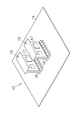
図1は電子機器の一具体例すなわちサーバコンピュータ装置11の外観を概略的に示す。サーバコンピュータ装置11は筐体12を備える。筐体12内には収容空間が区画される。収容空間にはマザーボードが配置される。マザーボードには例えば電子部品パッケージといった半導体部品やメインメモリが実装される。電子部品パッケージは、例えば一時的にメインメモリに保持されるソフトウェアプログラムやデータに基づき様々な演算処理を実行する。ソフトウェアプログラムやデータは、同様に収容空間に配置されるハードディスク駆動装置(HDD)といった大容量記憶装置に格納されればよい。こういったサーバコンピュータ装置11は例えばラックに搭載される。
FIG. 1 schematically shows an external appearance of a specific example of an electronic device, that is, a server computer device 11. The server computer device 11 includes a housing 12. A housing space is defined in the housing 12. A motherboard is disposed in the accommodation space. A semiconductor component such as an electronic component package and a main memory are mounted on the motherboard. The electronic component package executes various arithmetic processes based on, for example, software programs and data temporarily stored in the main memory. The software program and data may be stored in a large-capacity storage device such as a hard disk drive (HDD) that is similarly arranged in the accommodation space. Such a server computer device 11 is mounted on a rack, for example.
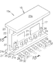
図2は本発明の本発明に係るプリント基板ユニットすなわちマザーボード13の外観を概略的に示す。このマザーボード13は大型のプリント配線板14を備える。プリント配線板14には例えば樹脂基板が用いられる。プリント配線板14の平坦な表面には表面実装型のプリント基板モジュール15が実装される。プリント基板モジュール15は、プリント配線板14の表面から直立するモールド16を備える。モールド16にはプリント基板17が保持される。プリント基板17は、プリント配線板14の表面から直立する垂直姿勢を確立する
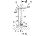
図3は本発明の第1実施形態に係るプリント基板モジュール15の構造を概略的に示す。このプリント基板モジュール15では、モールド16は、プリント配線板14の表面に沿って平たく広がる台座21を備える。台座21は、平坦な底面で対象物すなわちプリント配線板14の表面に受け止められる。こうして台座21はプリント配線板14の表面で自立する。モールド16は、一体成型に基づき台座21に一体化される側壁22を備える。側壁22は例えば平たい板状に形成される。側壁22は台座21の上面から垂直に立つ。台座21は、側壁22より前側の第1台座21aと、側壁22より後側の第2台座21bとを区画する。ここでは、台座21の長手方向に規定される第1方向に直交する第2方向に規定される第1台座21aの幅は、第2方向に規定される第2台座21bの幅より大きく設定される。
FIG. 2 schematically shows the appearance of the printed circuit board unit according to the present invention, that is, the mother board 13. The motherboard 13 includes a large printed wiring board 14. For example, a resin substrate is used for the printed wiring board 14. A surface mount type printed circuit board module 15 is mounted on the flat surface of the printed wiring board 14. The printed circuit board module 15 includes a mold 16 that stands upright from the surface of the printed wiring board 14. A printed circuit board 17 is held on the mold 16. The printed circuit board 17 establishes a vertical posture standing upright from the surface of the printed wiring board 14. FIG. 3 schematically shows the structure of the printed circuit board module 15 according to the first embodiment of the present invention. In the printed circuit board module 15, the mold 16 includes a pedestal 21 that spreads flat along the surface of the printed wiring board 14. The pedestal 21 is received on the surface of the object, that is, the printed wiring board 14 with a flat bottom surface. In this way, the base 21 is self-supporting on the surface of the printed wiring board 14. The mold 16 includes a side wall 22 that is integrated with the pedestal 21 based on integral molding. The side wall 22 is formed in a flat plate shape, for example. The side wall 22 stands vertically from the upper surface of the pedestal 21. The pedestal 21 defines a first pedestal 21 a on the front side of the side wall 22 and a second pedestal 21 b on the rear side of the side wall 22. Here, the width of the first pedestal 21a defined in the second direction orthogonal to the first direction defined in the longitudinal direction of the pedestal 21 is set larger than the width of the second pedestal 21b defined in the second direction. The
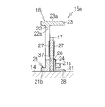
モールド16は、一体成型に基づき側壁22の上端に一体化される天板23を備える。天板23は台座21に平行に広がる。天板23は例えば平たい板状に形成される。天板23の上面には所定の広がりで上向きの平坦面23aが規定される。後述のように、平坦面23aは吸着面を形成する。こうしたモールド16は絶縁性の樹脂材料から一体成型される。台座21および天板23の間には所定の空間が形成される。この空間にはプリント基板17がはめ込まれる。プリント基板17の裏面は側壁22に受け止められる。こうしてプリント基板17は側壁22に沿って垂直姿勢を確立する。
The mold 16 includes a top plate 23 that is integrated with the upper end of the side wall 22 based on integral molding. The top plate 23 extends parallel to the pedestal 21. The top plate 23 is formed in a flat plate shape, for example. On the top surface of the top plate 23, an upward flat surface 23a is defined with a predetermined spread. As will be described later, the flat surface 23a forms an adsorption surface. Such a mold 16 is integrally molded from an insulating resin material. A predetermined space is formed between the base 21 and the top plate 23. A printed circuit board 17 is fitted in this space. The back surface of the printed circuit board 17 is received by the side wall 22. Thus, the printed circuit board 17 establishes a vertical posture along the side wall 22.
モールド16は、例えばプリント基板17の表面より前側で第1台座21aの表面から突き出る複数の導電端子24を備える。導電端子24は第1方向に配列される。各導電端子24は、プリント基板17の表面に形成される対応の導電パッド25に個別に電気接続される。電気接続の確立にあたってはんだ材26が用いられる。各導電パッド25は、例えばプリント基板17の表面や裏面に形成される配線パターン(図示されず)に接続される。こういった配線パターンは、プリント基板17の表面や裏面に実装される電子部品チップ27に接続される。
The mold 16 includes a plurality of conductive terminals 24 protruding from the surface of the first pedestal 21a on the front side of the surface of the printed circuit board 17, for example. The conductive terminals 24 are arranged in the first direction. Each conductive terminal 24 is individually electrically connected to a corresponding conductive pad 25 formed on the surface of the printed circuit board 17. Solder material 26 is used in establishing the electrical connection. Each conductive pad 25 is connected to a wiring pattern (not shown) formed on the front surface or the back surface of the printed circuit board 17, for example. Such a wiring pattern is connected to the electronic component chip 27 mounted on the front surface or the back surface of the printed circuit board 17.
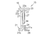
その一方で、モールド16は、台座21の底面を含む仮想平面に沿って第1台座21aから突き出る複数の表面実装端子28を備える。各表面実装端子28は、プリント配線板14の表面に形成される対応の導電パッド29に電気接続される。電気接続の確立にあたってはんだ材31が用いられる。導電パッド29には、プリント配線板14の表面に形成される対応の配線パターン32が接続される。図4に示されるように、側壁22は例えば枠体から形成される。こうして側壁22には貫通孔22aが形成される。貫通孔22a内にはプリント配線板14の裏面に実装される電子部品チップ27が受け入れられる。
On the other hand, the mold 16 includes a plurality of surface mount terminals 28 protruding from the first pedestal 21 a along a virtual plane including the bottom surface of the pedestal 21. Each surface mount terminal 28 is electrically connected to a corresponding conductive pad 29 formed on the surface of the printed wiring board 14. Solder material 31 is used in establishing the electrical connection. A corresponding wiring pattern 32 formed on the surface of the printed wiring board 14 is connected to the conductive pad 29. As shown in FIG. 4, the side wall 22 is formed from a frame, for example. Thus, a through hole 22 a is formed in the side wall 22. An electronic component chip 27 mounted on the back surface of the printed wiring board 14 is received in the through hole 22a.
図5に示されるように、導電端子24および対応の表面実装端子28は第1台座21a内で一体化される。すなわち、導電端子24および表面実装端子28は第1台座21a内に部分的に埋め込まれる。こうしてプリント配線板14上の他の電子部品(図示されず)はプリント基板17上の電子部品チップ27に接続される。導電端子24は、第1台座21aの表面に沿って延びる。導電端子24は弾性変形に基づきプリント基板17の下端を受け止める。弾性端子24の弾性力に基づきプリント基板17の上端は天板23に押し付けられる。こうしてプリント基板17は導電端子24および天板23の間に垂直姿勢ではめ込まれる。
As shown in FIG. 5, the conductive terminal 24 and the corresponding surface mount terminal 28 are integrated in the first pedestal 21a. That is, the conductive terminal 24 and the surface mount terminal 28 are partially embedded in the first pedestal 21a. In this way, other electronic components (not shown) on the printed wiring board 14 are connected to the electronic component chip 27 on the printed circuit board 17. The conductive terminal 24 extends along the surface of the first pedestal 21a. The conductive terminal 24 receives the lower end of the printed circuit board 17 based on elastic deformation. Based on the elastic force of the elastic terminal 24, the upper end of the printed circuit board 17 is pressed against the top plate 23. Thus, the printed circuit board 17 is fitted between the conductive terminals 24 and the top plate 23 in a vertical posture.
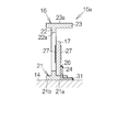
ここでは、第2台座21bの後縁から表面実装端子28の前端までのモールド16の幅は、プリント配線板14の表面から天板23までの高さの2分の1程度に設定されることが望ましい。こうした幅が設定されると、モールド16すなわちプリント基板モジュール15はプリント配線板14の表面で自立することができる。こうしてプリント基板モジュール15では、第1台座21aおよび表面実装端子28が協働で台座21の第1台足を構成する。同様に、第2台座21bは台座21の第2台足を構成する。第1台足および第2台足で台座21すなわちプリント基板モジュール15の自立を確立する。
Here, the width of the mold 16 from the rear edge of the second pedestal 21 b to the front end of the surface mounting terminal 28 is set to about one half of the height from the surface of the printed wiring board 14 to the top plate 23. Is desirable. When such a width is set, the mold 16, that is, the printed circuit board module 15 can stand on the surface of the printed wiring board 14. Thus, in the printed circuit board module 15, the first pedestal 21 a and the surface mount terminal 28 cooperate to constitute the first pedestal of the pedestal 21. Similarly, the second pedestal 21 b constitutes the second pedestal of the pedestal 21. The independence of the pedestal 21, that is, the printed circuit board module 15 is established by the first leg and the second leg.
図6に示されるように、プリント基板17の下端には複数の切り欠き33が規定される。切り欠き33はプリント基板17の輪郭を規定する。ここでは、各切り欠き33は例えば半円柱形の空間を規定する。各切り欠き33は対応の導電端子24を受け入れる。こうした切り欠き33の働きで第1方向にプリント基板17の変位は規制される。しかも、プリント基板17は導電端子24および天板23の間に挟み込まれる。その結果、モールド16からプリント基板17の脱落は回避される。プリント基板17の表面では各切り欠き33周りで前述の導電パッド25が形成される。
As shown in FIG. 6, a plurality of notches 33 are defined at the lower end of the printed circuit board 17. The notch 33 defines the outline of the printed circuit board 17. Here, each notch 33 defines a semi-cylindrical space, for example. Each notch 33 receives a corresponding conductive terminal 24. The displacement of the printed circuit board 17 is regulated in the first direction by the action of the notches 33. Moreover, the printed circuit board 17 is sandwiched between the conductive terminals 24 and the top plate 23. As a result, the printed board 17 is prevented from dropping from the mold 16. On the surface of the printed circuit board 17, the above-described conductive pad 25 is formed around each notch 33.
次にマザーボード13の製造方法を説明する。まず、プリント基板モジュール15が組み立てられる。図7に示されるように、モールド16では導電端子24は第1台座21aに表面に平行に延びる。傾斜姿勢のプリント基板17の下端が導電端子24に突き当てられる。導電端子24は切り欠き33に受け入れられる。こうしてプリント基板17はモールド16に対して正確に位置決めされる。導電端子24は弾性変形する。導電端子24を支点にプリント基板17は傾斜姿勢から垂直姿勢に向かって回転する。こうしてプリント基板17の裏面は側壁22に受け止められる。同時に、プリント基板17の上端は天板23に受け止められる。導電端子24の弾性変形に基づきプリント基板17は導電端子24および天板23の間にはめ込まれる。プリント基板17の導電パッド25上には予めはんだペースト34が塗布されればよい。
Next, a method for manufacturing the mother board 13 will be described. First, the printed circuit board module 15 is assembled. As shown in FIG. 7, in the mold 16, the conductive terminals 24 extend in parallel to the surface of the first pedestal 21a. The lower end of the inclined printed circuit board 17 is abutted against the conductive terminal 24. The conductive terminal 24 is received in the notch 33. Thus, the printed circuit board 17 is accurately positioned with respect to the mold 16. The conductive terminal 24 is elastically deformed. The printed circuit board 17 rotates from the inclined posture toward the vertical posture with the conductive terminal 24 as a fulcrum. Thus, the back surface of the printed circuit board 17 is received by the side wall 22. At the same time, the upper end of the printed circuit board 17 is received by the top plate 23. The printed circuit board 17 is fitted between the conductive terminal 24 and the top plate 23 based on the elastic deformation of the conductive terminal 24. The solder paste 34 may be applied in advance on the conductive pads 25 of the printed circuit board 17.
こうして組み立てられたプリント基板モジュール15はプリント配線板14上に運搬される。運搬にあたって、例えば図8に示されるように、天板23の平坦面23aには例えば自動実装ロボット35が吸着する。その一方で、プリント配線板14上では導電パッド29上に予めはんだペースト(図示されず)が塗布される。プリント配線板14上の所定の位置にプリント基板モジュール15が配置されると、表面実装端子28は導電パッド29上のはんだペーストに受け止められる。台座21の働きでプリント基板モジュール15は自立することができる。この状態でプリント配線板14にはリフロー工程が実施される。導電パッド25、29上のはんだペーストのはんだは溶融する。その後、冷却に基づきはんだは固化する。こうしてプリント基板モジュール15はプリント配線板14上に実装される。
The printed circuit board module 15 thus assembled is transported onto the printed wiring board 14. In carrying, for example, as shown in FIG. 8, for example, an automatic mounting robot 35 is attracted to the flat surface 23 a of the top plate 23. On the other hand, a solder paste (not shown) is previously applied on the conductive pads 29 on the printed wiring board 14. When the printed circuit board module 15 is disposed at a predetermined position on the printed wiring board 14, the surface mount terminals 28 are received by the solder paste on the conductive pads 29. The printed circuit board module 15 can stand by the function of the base 21. In this state, a reflow process is performed on the printed wiring board 14. The solder of the solder paste on the conductive pads 25 and 29 melts. Thereafter, the solder solidifies based on the cooling. Thus, the printed circuit board module 15 is mounted on the printed wiring board 14.
以上のようなプリント基板モジュール15によれば、台座21、側壁22および天板23は一体成型に基づき一体化されることから、簡単にプリント基板モジュール15は構成される。プリント基板17のはめ込みにあたって導電端子24が利用される。導電端子24の弾性力に基づきプリント基板17は導電端子24および天板23の間に確実に保持される。しかも、切り欠き33の働きでプリント基板17はモールド16に対して簡単に位置決めされる。
According to the printed circuit board module 15 as described above, since the pedestal 21, the side wall 22 and the top plate 23 are integrated based on integral molding, the printed circuit board module 15 is simply configured. The conductive terminal 24 is used for fitting the printed circuit board 17. The printed circuit board 17 is securely held between the conductive terminal 24 and the top plate 23 based on the elastic force of the conductive terminal 24. Moreover, the printed circuit board 17 is easily positioned with respect to the mold 16 by the action of the notches 33.
また、台座21の働きでプリント基板モジュール15はプリント配線板14上で自立することができる。プリント基板17は垂直姿勢を確立する。プリント配線板14上で実装面積は縮小される。実装密度は向上する。加えて、導電パッド25、29上にはんだペーストが塗布されることから、一度のリフロー工程でプリント基板モジュール15の実装が完了する。製造工程は簡略化される。しかも、天板23は自動実装ロボット35の吸着に用いられることができる。
Also, the printed circuit board module 15 can stand on the printed wiring board 14 by the function of the base 21. The printed circuit board 17 establishes a vertical posture. The mounting area is reduced on the printed wiring board 14. Mounting density is improved. In addition, since the solder paste is applied onto the conductive pads 25 and 29, the mounting of the printed circuit board module 15 is completed in a single reflow process. The manufacturing process is simplified. Moreover, the top plate 23 can be used for suction of the automatic mounting robot 35.
図9は本発明の第2実施形態に係るプリント基板モジュール15aの構造を概略的に示す。このプリント基板モジュール15aでは、第1台座21aがプリント配線板14の表面から所定の高さに配置される。第1台座21aおよび第2台座21bは相互に段違いに配置される。第1台座21aおよび天板23の間に形成される空間にプリント基板17が垂直姿勢ではめ込まれる。側壁22には1対の案内壁36、36が一体化される。案内壁36、36は側壁22の表面から突き出る。案内壁36、36同士の間にプリント基板17が収容される。案内壁36、36の働きで第1方向にプリント基板17は簡単に位置決めされる。
FIG. 9 schematically shows the structure of a printed circuit board module 15a according to the second embodiment of the present invention. In the printed circuit board module 15 a, the first pedestal 21 a is disposed at a predetermined height from the surface of the printed wiring board 14. The first pedestal 21a and the second pedestal 21b are arranged at different levels. The printed circuit board 17 is fitted in a vertical posture in a space formed between the first pedestal 21 a and the top plate 23. A pair of guide walls 36, 36 are integrated with the side wall 22. The guide walls 36, 36 protrude from the surface of the side wall 22. The printed circuit board 17 is accommodated between the guide walls 36 and 36. The printed circuit board 17 is easily positioned in the first direction by the action of the guide walls 36.
図10を併せて参照し、プリント基板17の表面の導電パッド29には第1台座21aの表面から突き出る導電端子24が押し当てられる。ここでは、導電パッド29はプリント基板17の下端の輪郭に沿って形成される。導電端子24の弾性力に基づきプリント基板17は側壁22に向かって押し付けられる。その一方で、表面実装端子28は、第1台座21aの裏面から突き出つつ、折れ曲がりに基づき前述の仮想平面に沿って延びる。その結果、表面実装端子28は、前述と同様に、台座21の第2台足を構成する。その他、前述のプリント基板モジュール15と均等な構成や構造には同一の参照符号が付される。こうしたプリント基板モジュール15aによれば、前述と同様の作用効果が実現される。
Referring also to FIG. 10, the conductive terminal 24 protruding from the surface of the first base 21 a is pressed against the conductive pad 29 on the surface of the printed circuit board 17. Here, the conductive pad 29 is formed along the contour of the lower end of the printed circuit board 17. The printed circuit board 17 is pressed toward the side wall 22 based on the elastic force of the conductive terminal 24. On the other hand, the surface mounting terminal 28 protrudes from the back surface of the first pedestal 21a and extends along the above-described virtual plane based on the bending. As a result, the surface mount terminal 28 forms the second foot of the base 21 as described above. Like reference numerals are attached to the structure or components equivalent to those of the aforementioned printed circuit board module 15. According to such a printed circuit board module 15a, the same effects as described above are realized.
プリント基板モジュール15aの組み立てにあたって、図11に示されるように、導電端子24の上端よりも上側でプリント基板17は側壁22に向かって押し当てられる。このとき、案内壁36、36の働きでプリント基板17は第1方向にモールド16に対して容易に位置決めされる。その後、プリント基板17は案内壁36、36の案内に基づき台座21に向かって押し下げられる。その結果、プリント基板17は導電端子24および側壁22の間に垂直姿勢ではめ込まれる。導電端子24はプリント基板17上の対応の導電パッド25上に位置決めされる。その後、前述と同様に、リフロー工程が実施されればよい。
In assembling the printed circuit board module 15a, the printed circuit board 17 is pressed toward the side wall 22 above the upper end of the conductive terminal 24, as shown in FIG. At this time, the printed circuit board 17 is easily positioned with respect to the mold 16 in the first direction by the action of the guide walls 36 and 36. Thereafter, the printed circuit board 17 is pushed down toward the base 21 based on the guidance of the guide walls 36 and 36. As a result, the printed circuit board 17 is fitted between the conductive terminal 24 and the side wall 22 in a vertical posture. The conductive terminals 24 are positioned on corresponding conductive pads 25 on the printed circuit board 17. Then, the reflow process should just be implemented similarly to the above-mentioned.
こういったプリント基板モジュール15aでは、図12に示されるように、プリント基板モジュール15と同様に、第1台座21aは第2台座21bと同じ高さに配置されてもよい。こうして、前述のプリント基板モジュール15と同様に、第1台座21aはプリント配線板14の表面に受け止められる。図13を併せて参照し、表面実装端子28は第1台座21aの前端から前述の仮想平面に沿って突き出る。その他、前述のプリント基板モジュール15と均等な構成や構造には同一の参照符号が付される。こうしたプリント基板モジュール15aによれば、前述と同様の作用効果が実現される。
In such a printed circuit board module 15a, as shown in FIG. 12, like the printed circuit board module 15, the first pedestal 21a may be arranged at the same height as the second pedestal 21b. In this way, the first pedestal 21 a is received on the surface of the printed wiring board 14 in the same manner as the printed circuit board module 15 described above. Referring also to FIG. 13, the surface mount terminal 28 protrudes from the front end of the first base 21 a along the above-described virtual plane. Like reference numerals are attached to the structure or components equivalent to those of the aforementioned printed circuit board module 15. According to such a printed circuit board module 15a, the same effects as described above are realized.
また、プリント基板モジュール15aでは、図14に示されるように、第1台座21aにその表面から裏面まで貫通する貫通孔37が形成されてもよい。貫通孔37はプリント基板17を受け入れる。このとき、側壁22では案内壁36、36の形成は省略されればよい。図15を併せて参照し、第1台座21aはプリント配線板14の表面から所定の高さに配置される。貫通孔37の働きで第1方向にプリント基板17は位置決めされる。その他、前述のプリント基板モジュール15と均等な構成や構造には同一の参照符号が付される。こうしたプリント基板モジュール15aによれば、前述と同様の作用効果が実現される。
Further, in the printed circuit board module 15a, as shown in FIG. 14, a through hole 37 penetrating from the front surface to the back surface may be formed in the first pedestal 21a. The through hole 37 receives the printed circuit board 17. At this time, the formation of the guide walls 36, 36 may be omitted from the side wall 22. Referring also to FIG. 15, the first pedestal 21 a is disposed at a predetermined height from the surface of the printed wiring board 14. The printed circuit board 17 is positioned in the first direction by the action of the through hole 37. Like reference numerals are attached to the structure or components equivalent to those of the aforementioned printed circuit board module 15. According to such a printed circuit board module 15a, the same effects as described above are realized.
図16は本発明の第3実施形態に係るプリント基板モジュール15bの構造を概略的に示す。このプリント基板モジュール15bはモールド41を備える。モールド41は台座42を備える。台座42は平坦な底面でプリント配線板14の表面に受け止められる。台座42は第1台足42aを有する。台座42には、前述と同様に、一体成型に基づき側壁22が一体化される。側壁22には一体成型に基づき天板23が一体化される。こうしたモールド41は絶縁性の樹脂材料から一体成型される。側壁22にはプリント基板17が保持される。プリント基板17は、天板23から台座42に向かって広がる。
FIG. 16 schematically shows the structure of a printed circuit board module 15b according to the third embodiment of the present invention. This printed circuit board module 15 b includes a mold 41. The mold 41 includes a pedestal 42. The pedestal 42 is received on the surface of the printed wiring board 14 with a flat bottom surface. The pedestal 42 has a first foot 42a. As described above, the side wall 22 is integrated with the pedestal 42 based on integral molding. A top plate 23 is integrated with the side wall 22 based on integral molding. Such a mold 41 is integrally molded from an insulating resin material. A printed circuit board 17 is held on the side wall 22. The printed circuit board 17 extends from the top plate 23 toward the base 42.
プリント基板17の表面に沿って複数の導電端子24が並列に延びる。導電端子24は前述のはんだ材26でプリント基板17上の導電パッド25に固定される。すべての導電端子24は保持モールド43で連結される。保持モールド43は絶縁性の樹脂材料から形成される。図17を併せて参照し、各導電端子24には対応の表面実装端子28が一体化される。表面実装端子28は、台座42の底面を含む仮想平面に沿って延びる。こうして表面実装端子28はプリント配線板14上の導電パッド29に接続される。表面実装端子28は第2台足を構成する。表面実装端子28は第1台足42aと協働で台座42すなわちプリント基板モジュール15bの自立を確立する。
A plurality of conductive terminals 24 extend in parallel along the surface of the printed circuit board 17. The conductive terminal 24 is fixed to the conductive pad 25 on the printed circuit board 17 by the solder material 26 described above. All the conductive terminals 24 are connected by a holding mold 43. The holding mold 43 is formed from an insulating resin material. Referring also to FIG. 17, a corresponding surface mount terminal 28 is integrated with each conductive terminal 24. The surface mounting terminal 28 extends along a virtual plane including the bottom surface of the base 42. Thus, the surface mounting terminals 28 are connected to the conductive pads 29 on the printed wiring board 14. The surface mount terminal 28 constitutes a second foot. The surface mount terminal 28 establishes self-support of the pedestal 42, that is, the printed circuit board module 15b, in cooperation with the first foot 42a.
図18を併せて参照し、プリント基板17の保持にあたって、側壁22の表面から突起44が突き出る。突起44は側壁22の表面で四隅に配置される。突起44は、表面から裏面までプリント基板17を貫通する貫通孔45に受け入れられる。突起44は、内向き面で相互に向き合う1対の軸部材46を備える。軸部材46は弾性変形することができる。軸部材46の先端にはプリント基板17の表面に係り合う係止片46aが区画される。係止片46aの働きで突起44からプリント基板17の脱落は回避される。こうしてプリント基板17は側壁22すなわちモールド41に保持される。
Referring also to FIG. 18, when holding the printed circuit board 17, the protrusion 44 protrudes from the surface of the side wall 22. The protrusions 44 are arranged at the four corners on the surface of the side wall 22. The protrusion 44 is received in the through hole 45 that penetrates the printed circuit board 17 from the front surface to the back surface. The protrusion 44 includes a pair of shaft members 46 that face each other on an inward surface. The shaft member 46 can be elastically deformed. A locking piece 46 a that engages with the surface of the printed circuit board 17 is defined at the tip of the shaft member 46. Due to the action of the locking piece 46a, the printed board 17 is prevented from falling off from the protrusion 44. Thus, the printed circuit board 17 is held on the side wall 22, that is, the mold 41.
こういったプリント基板モジュール15bの組み立てにあたって、まず、プリント基板17の表面に導電端子24がはんだ付けされる。導電端子24は保持モールド43に保持される。その後、プリント基板17はモールド41に取り付けられる。取り付けにあたって、貫通孔45は突起44上に位置決めされる。図19に示されるように、係止片46aが貫通孔45の開口に押し当てられると、軸部材46の弾性変形に基づき係止片46a同士は相互に近づく。その結果、係止片46aは貫通孔45内に受け入れられる。係止片46aが貫通孔45から出ると、軸部材46の弾性復元力に基づき係止片46aはプリント基板17の表面に受け止められる。こうしてプリント基板17はモールド41に保持される。こうしてプリント基板モジュール15bは組み立てられる。
In assembling such a printed circuit board module 15 b, first, the conductive terminals 24 are soldered to the surface of the printed circuit board 17. The conductive terminal 24 is held by the holding mold 43. Thereafter, the printed circuit board 17 is attached to the mold 41. In mounting, the through hole 45 is positioned on the protrusion 44. As shown in FIG. 19, when the locking piece 46 a is pressed against the opening of the through hole 45, the locking pieces 46 a come closer to each other based on the elastic deformation of the shaft member 46. As a result, the locking piece 46 a is received in the through hole 45. When the locking piece 46 a comes out of the through hole 45, the locking piece 46 a is received on the surface of the printed circuit board 17 based on the elastic restoring force of the shaft member 46. In this way, the printed circuit board 17 is held by the mold 41. Thus, the printed circuit board module 15b is assembled.
以上のようなプリント基板モジュール15bによれば、台座42、側壁22および天板23は一体成型に基づき一体化されることから、簡単にプリント基板モジュール15bは構成される。しかも、プリント基板17のはめ込みにあたって突起44が用いられる。突起44の働きでプリント基板17はモールド41に対して簡単に位置決めされる。また、台座42および表面実装端子28の働きでプリント基板モジュール15bはプリント配線板14上で自立することができる。実装密度は向上する。加えて、前述と同様に、天板23は自動実装ロボット35の吸着に用いられる。
According to the printed circuit board module 15b as described above, since the pedestal 42, the side wall 22 and the top plate 23 are integrated based on integral molding, the printed circuit board module 15b is simply configured. Moreover, the protrusions 44 are used for fitting the printed circuit board 17. The printed circuit board 17 is easily positioned with respect to the mold 41 by the action of the protrusions 44. Further, the printed circuit board module 15 b can stand on the printed wiring board 14 by the action of the base 42 and the surface mounting terminals 28. Mounting density is improved. In addition, the top plate 23 is used for suction of the automatic mounting robot 35 as described above.
こうしたプリント基板モジュール15bでは、モールド41は例えば金属材料から形成されてもよい。金属材料には例えばアルミニウムや銅が含まれる。前述のように、プリント基板17は側壁22に受け止められる。マザーボード13の動作時、電子部品チップ27は発熱に基づき熱エネルギーを生成する。熱エネルギーはプリント基板17を介して側壁22すなわちモールド41に伝達される。熱エネルギーは比較的に大きな表面積を有するモールド41から大気に放射される。こうして電子部品チップ27の過度の温度上昇は阻止される。
In such a printed circuit board module 15b, the mold 41 may be formed of, for example, a metal material. Examples of the metal material include aluminum and copper. As described above, the printed circuit board 17 is received by the side wall 22. During the operation of the mother board 13, the electronic component chip 27 generates heat energy based on heat generation. Thermal energy is transmitted to the side wall 22, that is, the mold 41 through the printed circuit board 17. Thermal energy is radiated from the mold 41 having a relatively large surface area to the atmosphere. Thus, an excessive temperature rise of the electronic component chip 27 is prevented.