WO2013086746A1 - 液晶显示面板以及其制造方式 - Google Patents
液晶显示面板以及其制造方式 Download PDFInfo
- Publication number
- WO2013086746A1 WO2013086746A1 PCT/CN2011/084183 CN2011084183W WO2013086746A1 WO 2013086746 A1 WO2013086746 A1 WO 2013086746A1 CN 2011084183 W CN2011084183 W CN 2011084183W WO 2013086746 A1 WO2013086746 A1 WO 2013086746A1
- Authority
- WO
- WIPO (PCT)
- Prior art keywords
- layer
- thin film
- film transistor
- glass substrate
- liquid crystal
- Prior art date
- Legal status (The legal status is an assumption and is not a legal conclusion. Google has not performed a legal analysis and makes no representation as to the accuracy of the status listed.)
- Ceased
Links
Images




Classifications
-
- G—PHYSICS
- G02—OPTICS
- G02F—OPTICAL DEVICES OR ARRANGEMENTS FOR THE CONTROL OF LIGHT BY MODIFICATION OF THE OPTICAL PROPERTIES OF THE MEDIA OF THE ELEMENTS INVOLVED THEREIN; NON-LINEAR OPTICS; FREQUENCY-CHANGING OF LIGHT; OPTICAL LOGIC ELEMENTS; OPTICAL ANALOGUE/DIGITAL CONVERTERS
- G02F1/00—Devices or arrangements for the control of the intensity, colour, phase, polarisation or direction of light arriving from an independent light source, e.g. switching, gating or modulating; Non-linear optics
- G02F1/01—Devices or arrangements for the control of the intensity, colour, phase, polarisation or direction of light arriving from an independent light source, e.g. switching, gating or modulating; Non-linear optics for the control of the intensity, phase, polarisation or colour
- G02F1/13—Devices or arrangements for the control of the intensity, colour, phase, polarisation or direction of light arriving from an independent light source, e.g. switching, gating or modulating; Non-linear optics for the control of the intensity, phase, polarisation or colour based on liquid crystals, e.g. single liquid crystal display cells
- G02F1/133—Constructional arrangements; Operation of liquid crystal cells; Circuit arrangements
- G02F1/136—Liquid crystal cells structurally associated with a semi-conducting layer or substrate, e.g. cells forming part of an integrated circuit
- G02F1/1362—Active matrix addressed cells
- G02F1/136209—Light shielding layers, e.g. black matrix, incorporated in the active matrix substrate, e.g. structurally associated with the switching element
-
- H—ELECTRICITY
- H10—SEMICONDUCTOR DEVICES; ELECTRIC SOLID-STATE DEVICES NOT OTHERWISE PROVIDED FOR
- H10D—INORGANIC ELECTRIC SEMICONDUCTOR DEVICES
- H10D30/00—Field-effect transistors [FET]
- H10D30/60—Insulated-gate field-effect transistors [IGFET]
- H10D30/67—Thin-film transistors [TFT]
- H10D30/6704—Thin-film transistors [TFT] having supplementary regions or layers in the thin films or in the insulated bulk substrates for controlling properties of the device
- H10D30/6723—Thin-film transistors [TFT] having supplementary regions or layers in the thin films or in the insulated bulk substrates for controlling properties of the device having light shields
-
- H—ELECTRICITY
- H10—SEMICONDUCTOR DEVICES; ELECTRIC SOLID-STATE DEVICES NOT OTHERWISE PROVIDED FOR
- H10D—INORGANIC ELECTRIC SEMICONDUCTOR DEVICES
- H10D86/00—Integrated devices formed in or on insulating or conducting substrates, e.g. formed in silicon-on-insulator [SOI] substrates or on stainless steel or glass substrates
- H10D86/01—Manufacture or treatment
- H10D86/021—Manufacture or treatment of multiple TFTs
-
- H—ELECTRICITY
- H10—SEMICONDUCTOR DEVICES; ELECTRIC SOLID-STATE DEVICES NOT OTHERWISE PROVIDED FOR
- H10D—INORGANIC ELECTRIC SEMICONDUCTOR DEVICES
- H10D86/00—Integrated devices formed in or on insulating or conducting substrates, e.g. formed in silicon-on-insulator [SOI] substrates or on stainless steel or glass substrates
- H10D86/40—Integrated devices formed in or on insulating or conducting substrates, e.g. formed in silicon-on-insulator [SOI] substrates or on stainless steel or glass substrates characterised by multiple TFTs
-
- H—ELECTRICITY
- H10—SEMICONDUCTOR DEVICES; ELECTRIC SOLID-STATE DEVICES NOT OTHERWISE PROVIDED FOR
- H10D—INORGANIC ELECTRIC SEMICONDUCTOR DEVICES
- H10D86/00—Integrated devices formed in or on insulating or conducting substrates, e.g. formed in silicon-on-insulator [SOI] substrates or on stainless steel or glass substrates
- H10D86/40—Integrated devices formed in or on insulating or conducting substrates, e.g. formed in silicon-on-insulator [SOI] substrates or on stainless steel or glass substrates characterised by multiple TFTs
- H10D86/441—Interconnections, e.g. scanning lines
-
- H—ELECTRICITY
- H10—SEMICONDUCTOR DEVICES; ELECTRIC SOLID-STATE DEVICES NOT OTHERWISE PROVIDED FOR
- H10D—INORGANIC ELECTRIC SEMICONDUCTOR DEVICES
- H10D86/00—Integrated devices formed in or on insulating or conducting substrates, e.g. formed in silicon-on-insulator [SOI] substrates or on stainless steel or glass substrates
- H10D86/40—Integrated devices formed in or on insulating or conducting substrates, e.g. formed in silicon-on-insulator [SOI] substrates or on stainless steel or glass substrates characterised by multiple TFTs
- H10D86/481—Integrated devices formed in or on insulating or conducting substrates, e.g. formed in silicon-on-insulator [SOI] substrates or on stainless steel or glass substrates characterised by multiple TFTs integrated with passive devices, e.g. auxiliary capacitors
-
- H—ELECTRICITY
- H10—SEMICONDUCTOR DEVICES; ELECTRIC SOLID-STATE DEVICES NOT OTHERWISE PROVIDED FOR
- H10D—INORGANIC ELECTRIC SEMICONDUCTOR DEVICES
- H10D86/00—Integrated devices formed in or on insulating or conducting substrates, e.g. formed in silicon-on-insulator [SOI] substrates or on stainless steel or glass substrates
- H10D86/40—Integrated devices formed in or on insulating or conducting substrates, e.g. formed in silicon-on-insulator [SOI] substrates or on stainless steel or glass substrates characterised by multiple TFTs
- H10D86/60—Integrated devices formed in or on insulating or conducting substrates, e.g. formed in silicon-on-insulator [SOI] substrates or on stainless steel or glass substrates characterised by multiple TFTs wherein the TFTs are in active matrices
-
- G—PHYSICS
- G02—OPTICS
- G02F—OPTICAL DEVICES OR ARRANGEMENTS FOR THE CONTROL OF LIGHT BY MODIFICATION OF THE OPTICAL PROPERTIES OF THE MEDIA OF THE ELEMENTS INVOLVED THEREIN; NON-LINEAR OPTICS; FREQUENCY-CHANGING OF LIGHT; OPTICAL LOGIC ELEMENTS; OPTICAL ANALOGUE/DIGITAL CONVERTERS
- G02F1/00—Devices or arrangements for the control of the intensity, colour, phase, polarisation or direction of light arriving from an independent light source, e.g. switching, gating or modulating; Non-linear optics
- G02F1/01—Devices or arrangements for the control of the intensity, colour, phase, polarisation or direction of light arriving from an independent light source, e.g. switching, gating or modulating; Non-linear optics for the control of the intensity, phase, polarisation or colour
- G02F1/13—Devices or arrangements for the control of the intensity, colour, phase, polarisation or direction of light arriving from an independent light source, e.g. switching, gating or modulating; Non-linear optics for the control of the intensity, phase, polarisation or colour based on liquid crystals, e.g. single liquid crystal display cells
- G02F1/133—Constructional arrangements; Operation of liquid crystal cells; Circuit arrangements
- G02F1/136—Liquid crystal cells structurally associated with a semi-conducting layer or substrate, e.g. cells forming part of an integrated circuit
- G02F1/1362—Active matrix addressed cells
- G02F1/136222—Colour filters incorporated in the active matrix substrate
Definitions
- the present invention relates to a liquid crystal display panel and related manufacturing method, and more particularly to a liquid crystal display panel using a metal layer instead of a conventional black matrix layer and related manufacturing methods.
- LCD monitors have become widely used in a wide range of electronic devices such as mobile phones, personal digital assistants (PDAs), digital cameras, computer screens or laptop screens. Rate display with color screen.
- a conventional liquid crystal display panel is composed of a color filter and a thin film transistor matrix substrate (thin a film transistor array substrate, a TFT array substrate, and a liquid crystal layer disposed between the two substrates Crystal Layer).
- a liquid crystal display panel has a poor resolution and a low aperture ratio of a pixel, and it is easy to have a misalignment when the color filter substrate is bonded to the thin film transistor matrix substrate.
- FIG. 1 is a simplified cross-sectional view of a prior art liquid crystal display panel 100.
- the liquid crystal display panel 100 is a BOA liquid crystal display panel, that is, the color filter layer 130 is directly fabricated on the glass substrate 110 of the liquid crystal display panel 100.
- the liquid crystal display panel 100 includes a glass substrate 110 , a black matrix layer 120 , and a color filter layer 130 .
- the upper liquid crystal display panel 100 will include these structures, and its function and structure are also known in the art, and will not be further described herein for the sake of brevity.
- the color filter layer 130 is used for filtering, so that the light passing through the color filter layer 130 is visible light of a specific color.
- the light passing through the red, blue, and green filter units 131, 132, and 133 is red, blue, and green, respectively. In this way, by mixing the light of the three primary colors, light of various colors can be synthesized to display the image to be presented.
- the black matrix layer 120 is located between the color filter layers 130 to block the light emitted by the backlight module to prevent the light from passing through the plurality of color filter layers 130 erroneously, thereby avoiding false color mixing and light leakage.
- FIG. 2 is a simplified cross-sectional view of another prior art liquid crystal display panel 200.
- FIG. 2 is similar to the architecture of FIG. 1. Both components having the same reference numerals have the same functions and structures, and therefore will not be further described.
- a layer of overcoat 210 is deposited, which makes the height difference of the substrate smaller and makes the substrate more flat. In this way, the difference in the height difference of the substrate can be reduced, resulting in poor alignment of the liquid crystal molecules, thereby reducing the light leakage.
- Today's liquid crystal display panels are mass produced through multiple processes. If the use of the black matrix layer can be reduced, the process cost can be reduced, and a cheaper liquid crystal display panel can be manufactured.
- the invention discloses a manufacturing method of a liquid crystal display panel, which is applied to a COA (color filter).
- the manufacturing process includes the following steps: providing a glass substrate; the manufacturing method further comprises: forming a first metal layer on the glass substrate, and etching the first metal layer to form a a scan line, a gate of a thin film transistor, and a lower electrode of the storage capacitor; depositing an insulating layer on the glass substrate and the first metal layer; depositing an active layer and an ohmic contact on the insulating layer a layer; etching the active layer and the ohmic contact layer to define the thin film transistor, wherein the active layer serves as a channel of the thin film transistor; depositing a layer on the ohmic contact layer and the insulating layer a second metal layer, and etching the second metal layer to form a data line, and defining a source and a drain of the thin film transistor on the ohmic contact layer; and the second metal layer and the Depositing
- the manufacturing method further comprises: depositing a transparent material layer on the transparent conductive layer.
- the plurality of filter units comprise a red filter unit, a green filter unit, and a blue filter unit.
- the present invention further provides a manufacturing method of a liquid crystal display panel, which is applied to COA (color Filter on The manufacturing process includes the following steps: providing a glass substrate; the manufacturing method further comprises: forming a scan line, a thin film transistor, a data line, and a storage capacitor under the electrode; depositing a protective layer, And etching the protective layer to form a first opening on the drain of the thin film transistor, and forming a second opening above the lower electrode of the storage capacitor; depositing a color on the protective layer And filtering a color filter layer to form a plurality of filter units; and depositing a transparent conductive layer on the color filter layer, wherein the transparent conductive layer is coupled to the first opening a drain of the thin film transistor, and forming an upper electrode of the storage capacitor at the second opening; wherein the data line or the scan line between each two adjacent filter units is projected in the The area of the glass substrate overlaps the area where the two adjacent filter units are projected on the glass substrate.
- the manufacturing method further comprises: depositing a transparent material layer on the transparent conductive layer.
- the plurality of filter units comprise a red filter unit, a green filter unit, and a blue filter unit.
- the present invention further provides a liquid crystal display panel comprising: a glass substrate; a first metal layer on the glass substrate for forming a scan line, a gate of a thin film transistor And a storage capacitor lower electrode; an insulating layer on the glass substrate and the first metal layer; an active layer on the insulating layer for use as a channel of the thin film transistor; an ohmic contact a layer on the active layer; a second metal layer on the ohmic contact layer and the insulating layer for use as a data line, a source and a drain of a thin film transistor; a protective layer located at the a second metal layer and the insulating layer; a color filter layer on the protective layer, comprising a plurality of filter units, wherein the data line between each two adjacent filter units or The scan line is projected on a region of the glass substrate overlapping a region projected by each two adjacent filter units on the glass substrate; and a transparent conductive layer is disposed on the color filter layer and coupled The drain of the thin
- the liquid crystal display panel further comprises: a transparent material layer on the transparent conductive layer.
- the plurality of filter units comprise a red unit, a green filter unit, and a blue filter unit.
- the present invention replaces the function of the traditional black matrix layer with a metal layer as a data line or a scan line, so that a black matrix process can be omitted, which makes the process easier and not only improved. Yield, and further reduce costs.
- FIG. 1 is a simplified cross-sectional view of a prior art liquid crystal display panel.
- FIG. 2 is a simplified cross-sectional view of another prior art liquid crystal display panel.
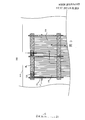
- FIG 3 is a schematic view of a liquid crystal display panel according to an embodiment of the present invention.
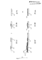
- 4A-4C to 9A-9C illustrate a method of fabricating the liquid crystal display panel of FIG. 3.
- FIG. 3 is a schematic diagram of a liquid crystal display panel 300 according to an embodiment of the present invention.
- the liquid crystal display panel 300 includes a glass substrate 310, a plurality of scanning lines SL, a plurality of data lines DL, a plurality of thin film transistors 220, a plurality of common electrodes CL, and a plurality of pixel electrodes 360.
- the scan line SL, the data line DL, and the thin film transistor 220 are all disposed on the glass substrate 310, and the scan line SL and the data line DL are alternately arranged in a matrix region arranged in a matrix.
- Each of the thin film transistors 220 is electrically connected to a pixel electrode 360, a scan line SL, and a data line DL.
- Figures 4A-4C are cross-sectional views of the liquid crystal display panel 300 of Figure 3 taken along line A-A', B-B', and C-C'.
- the liquid crystal display panel 300 includes a glass substrate 310 , an insulating layer 320 , a thin film transistor 220 , a protective layer 340 , and a plurality of filter units 350 .
- the liquid crystal display panel 300 is a COA liquid crystal display panel, that is, the plurality of filter units 350 and the thin film transistors 220 are formed on the same glass substrate 310.
- the scanning line SL, the gate electrode 221 of the thin film transistor 220, and the common electrode CL are located on the glass substrate 310, and are composed of the same first metal layer.
- the insulating layer 320 is located on the glass substrate 310 and the first metal layer.
- Active layer The layer 541 is located on the insulating layer 320 and serves as the channel 224 of the thin film transistor 220.
- An ohmic contact layer 542 is located on the active layer 541.
- the second metal layer is located on the ohmic contact layer 542 and the insulating layer 320 and serves as the data line DL and the source 222 and the drain 223 of the thin film transistor 220.
- the protective layer 340 is located on the second metal layer and the insulating layer 320.
- the filter unit 350 is located on the protective layer 340.
- An overcoat 460 is disposed on the filter unit 350 for flattening the area above the filter unit 350, thereby facilitating the reduction of light leakage caused by the reverse turbulence of the liquid crystal molecules.
- the transparent conductive layer 360 is disposed on the transparent material layer 460 and coupled to the drain 223 of the thin film transistor 220 for use as an upper electrode of the storage capacitor.
- the plurality of filter units 350 include a red filter unit, a blue filter unit, and a green filter unit for filtering light so that the passing light becomes red light, blue light, and green light to synthesize the desired image.
- the liquid crystal display panel 300 is divided into a pixel matrix in such a manner that the data lines DL and the scanning lines SL are vertically interlaced. These data lines DL and scan lines SL are located between two adjacent filter units 350, and these data lines DL and scan lines SL made of metal have the effect of blocking light.
- each of the filter units 350 forms an approximately trapezoidal oblique angle L when formed, liquid crystal molecules may discrelate the disorder in these oblique regions to cause poor light leakage.
- the data line DL and the scan line SL located between each two adjacent filter units 350 are projected on the area of the glass substrate 310 overlapping the area where the two adjacent filter units 350 are projected on the glass substrate 310. Since the data line DL and the scan line SL are made of metal, they have a good light-shielding effect, and after forming an overlapping area with the filter unit 350, light leakage between the filter units 350 can be prevented and the liquid crystal molecules can be prevented from being reversed. Light leakage can also suppress color mixing between the filter units 350 at the same time.
- the present invention replaces the functions of the prior art black matrix layer with the data line DL and the scan line SL, so that the present invention can achieve the purpose of preventing light leakage and color mixing without requiring a black matrix layer.
- the present invention can eliminate the process of the black matrix layer, making the process procedure simpler, which not only improves the yield but also reduces the manufacturing cost.
- 4A-4C to 9A-9C, 4A-4C to 9A-9C illustrate a manufacturing method of the liquid crystal display panel 300 shown in FIG.
- a first metal layer is first formed on the glass substrate 310 on the glass substrate 310, and the first metal layer is etched to form a scan line SL, a thin film transistor.
- the gate 221 of 220 and the common electrode CL also as the lower electrode of the storage capacitor).
- an insulating layer is deposited (insulating The layer 320 is on the glass substrate 310 and the first metal layer.
- an active layer 541 and an ohmic contact layer (n+) are deposited on the insulating layer 320.
- a second metal layer (M2) 532 is deposited on the ohmic contact layer 542 and the insulating layer 320, and the second metal layer is etched to form the data line DL and the ohmic contact layer 542.
- a source 222 and a drain 223 of the thin film transistor 220 are defined.
- a protective layer (passivation) is deposited on the ohmic contact layer 542 and the insulating layer 320.
- a protective layer 340 is formed to form a first opening 231 on the drain 223 of the thin film transistor 220 and a second opening 232 above the common electrode CL.
- a color filter layer is deposited over the protective layer 340, and the color filter layer is etched to form a plurality of filter units 350.
- a transparent material layer 460 is deposited on the filter unit 350.
- a transparent conductive layer 360 is deposited on the transparent material layer 460.
- the transparent conductive layer 360 is coupled to the drain 223 of the thin film transistor 220 through the first opening 231.
- the transparent conductive layer 360 forms an upper electrode of the storage capacitor at the second opening 232.
- the data line DL and the scan line SL located between each two adjacent filter units 350 are projected on the area of the glass substrate 310 overlapping the area where the two adjacent filter units 350 are projected on the glass substrate 310. Since the data line DL and the scan line SL are made of metal, they can be used to block light.
Landscapes
- Physics & Mathematics (AREA)
- Nonlinear Science (AREA)
- Liquid Crystal (AREA)
- Engineering & Computer Science (AREA)
- Microelectronics & Electronic Packaging (AREA)
- Mathematical Physics (AREA)
- Chemical & Material Sciences (AREA)
- Crystallography & Structural Chemistry (AREA)
- General Physics & Mathematics (AREA)
- Optics & Photonics (AREA)
- Devices For Indicating Variable Information By Combining Individual Elements (AREA)
Abstract
一种液晶显示面板结构以及其相关的制造方式,其应用于COA的制程,液晶显示面板(300)包含有玻璃基板(310)、绝缘层(320)、薄膜晶体管(220)、保护层(340)以及多个滤光单元(350)。液晶显示面板(300)使用滤光单元(350)与玻璃基板(310)间的金属层(用来构成数据线与扫描线)来阻挡光线,以达到防止混色与漏光的目的,因此,金属层可以用来取代习知黑色矩阵层的功能,这样可以省去一道黑色矩阵的制程,如此可以使制程更加简易,不但提升了良率,并且进一步地降低了成本。
Description
本发明涉及一种液晶显示面板以及其相关制造方式,尤指一种利用金属层来取代习知黑色矩阵层的液晶显示面板以及相关制造方式。
功能先进的显示器渐成为现今消费电子产品的重要特色,其中液晶显示器已经逐渐成为各种电子设备如移动电话、个人数字助理(PDA)、数字相机、计算机屏幕或笔记本电脑屏幕所广泛应用具有高分辨率彩色屏幕的显示器。
传统的液晶显示面板是由一彩色滤光基板(color filter)、一薄膜晶体管矩阵基板(thin
film transistor array substrate, TFT array substrate)以及一配置于此两基板间的液晶层(liquid
crystal
layer)所构成。然而,此种液晶显示面板的分辨率(resolution)较差、像素(pixel)的开口率较低,且彩色滤光基板与薄膜晶体管矩阵基板接合时容易有对位误差(misalignment)。
近年来,更提出了将彩色滤光层直接整合于薄膜晶体管矩阵基板上(Color Filter on Array,
COA)或是将黑色矩阵层制作于薄膜晶体管矩阵基板上(Black matrix on Array,
BOA)的技术,将COA基板或BOA基板与另一不具备彩色滤光层或黑矩阵层的对向基板组立,并于两基板间填入液晶分子,以形成液晶显示面板。由于彩色滤光层是仅直接形成于薄膜晶体管阵列基板上,因此不会产生对位误差。而且,此种液晶显示面板可具有较佳的分辨率且其像素的开口率亦较高。
请参阅图1,图1是现有技术液晶显示面板100的简易剖面图。如图1所示,液晶显示面板100为一BOA液晶显示面板,亦即,液晶显示面板100的玻璃基板110上,会直接制造彩色滤光层130。如图1所示,液晶显示面板100包含有玻璃基板110,黑色矩阵层120以及彩色滤光层130。
在此请注意,于图1之中,并未绘示彩色滤光层130与玻璃基板110间的金属层(用来构成数据线与扫描线)、绝缘层与保护层等等;然而,实际上液晶显示面板100会包含这些结构,且其功能与结构也以为业界所习知,为了简便说明,便不另赘述于此。
请继续参阅图1,彩色滤光层130是用来进行滤光,使得通过彩色滤光层130后的光线为特定颜色的可见光。以本实施例来说,通过红、蓝、绿色滤光单元131、132、133的光线便分别为红光、蓝光、绿光。如此一来,将此三原色的光线加以混合,便可合成各种颜色的光,以显示欲呈现的影像。
此外,黑色矩阵层120位于各彩色滤光层130之间,是用来阻挡由背光模块发出的光,以防止光线错误地通过数个彩色滤光层130,进而避免错误的混色以及漏光。
在此请参阅图2,图2是另一现有技术液晶显示面板200的简易剖面图。基本上,图2与图1的架构类似,两者具有相同标号的组件代表着彼此具有相同的功能与结构,故不另赘述。在此请注意,于图2之中,于彩色滤光层120之上,另沉积了一层透明材料层(overcoat)210,此透明材料层使得基板的高度差距变小,使基板更加平坦化,如此可减少由于基板的高度段差,造成液晶分子定向不良的情形,进而减少漏光的情形。
现今液晶显示面板是通过多道制程而大量生产。如果能减少黑色矩阵层的使用,将可以减少制程成本,而制造出更便宜的液晶显示面板。
因此本发明的目的是提供一种液晶显示面板以及其相关制造方法,其使用金属层来取代习知黑色矩阵层的液晶显示面板以及相关制造方式,有利于减低成本并减少制程。
根据本发明的一实施例,本发明揭示一种液晶显示面板的制造方式,其应用于COA(color filter
on
array)的制程,所述制造方式包括下列步骤:提供一玻璃基板;所述制造方式另包含:形成一第一金属层于所述玻璃基板上,并蚀刻所述第一金属层,以形成一扫描线、一薄膜晶体管的栅极以及一储存电容的下电极;沉积一绝缘层于所述玻璃基板以及所述第一金属层上;于所述绝缘层上,沉积一主动层以及一欧姆接触层;蚀刻所述主动层以及所述欧姆接触层,以定义出所述薄膜晶体管,其中所述主动层作为所述薄膜晶体管的通道;于所述欧姆接触层以及所述绝缘层上沉积一第二金属层,并蚀刻所述第二金属层,以形成一数据线,并于所述欧姆接触层上定义出所述薄膜晶体管的源极与漏极;于所述第二金属层以及所述绝缘层上沉积一保护层;蚀刻所述保护层,以于所述薄膜晶体管的漏极上形成一第一开口,以及于所述储存电容的下电极的上方,形成一第二开口;于所述保护层上面沉积一彩色滤光层,并蚀刻所述彩色滤光层以形成多个滤光单元;以及于所述彩色滤光层上沉积一透明导电层,所述透明导电层藉由所述第一开口耦接至所述薄膜晶体管的漏极,并于所述第二开口形成所述储存电容的上电极,其中所述第一金属层与所述第二金属层可用来阻挡光线。
根据本发明的一实施例,所述制造方式另包含:于所述透明导电层之上另沉积一透明材料层。
根据本发明的一实施例,所述多个滤光单元包括红色滤光单元、绿色滤光单元以及蓝色滤光单元。
根据本发明的一实施例,本发明另提供一种液晶显示面板的制造方式,其应用于COA(color
filter on
array)的制程,所述制造方式包括下列步骤:提供一玻璃基板;所述制造方式另包含:形成一扫描线、一薄膜晶体管、一数据线以及一储存电容之下电极;沉积一保护层,并蚀刻所述保护层,以于所述薄膜晶体管的漏极上形成一第一开口,以及于所述储存电容的下电极的上方,形成一第二开口;于所述保护层上面沉积一彩色滤光层,并蚀刻所述彩色滤光层以形成多个滤光单元;以及于所述彩色滤光层上沉积一透明导电层,所述透明导电层藉由所述第一开口耦接至薄膜晶体管的漏极,并于所述第二开口形成所述储存电容的上电极;其中位于每两个相邻滤光单元之间的所述数据线或所述扫描线,其投影在所述玻璃基板的区域重叠于每两个相邻滤光单元投影在所述玻璃基板的区域。
根据本发明的一实施例,所述制造方式另包含:于所述透明导电层之上另沉积一透明材料层。
根据本发明的一实施例,所述多个滤光单元包括红色滤光单元、绿色滤光单元以及蓝色滤光单元。
根据本发明的一实施例,本发明又提供一种液晶显示面板,包含:一玻璃基板;一第一金属层,位于所述玻璃基板上,用来形成一扫描线、一薄膜晶体管的栅极以及一储存电容之下电极;一绝缘层,位于所述玻璃基板以及所述第一金属层上;一主动层,位于所述绝缘层上,用来作为所述薄膜晶体管的通道;一欧姆接触层,位于所述主动层上;一第二金属层,位于所述欧姆接触层以及所述绝缘层上,用来作为一数据线、薄膜晶体管的源极与漏极;一保护层,位于所述第二金属层以及所述绝缘层上;一彩色滤光层,位于所述保护层上,包含多个滤光单元,其中位于每两个相邻滤光单元之间的所述数据线或所述扫描线,其投影在所述玻璃基板的区域重叠于每两个相邻滤光单元投影在所述玻璃基板的区域;以及一透明导电层,位于所述彩色滤光层上,耦接至所述薄膜晶体管的漏极,用来作为所述储存电容的上电极;其中所述第一金属层与所述第二金属层可用来阻挡光线。
根据本发明的一实施例,所述液晶显示面板另包含:一透明材料层,位于所述透明导电层之上。
根据本发明的一实施例,所述多个滤光单元包括红色单元、绿色滤光单元以及蓝色滤光单元。
相较于现有技术,本发明利用作为数据线或是扫描线的金属层来取代传统的黑色矩阵层的功能,这样可以省去一道黑色矩阵的制程,如此可以使制程更加简易,不但提升了良率,并且进一步地降低了成本。
图1是现有技术液晶显示面板的简易剖面图。
图2是另一现有技术液晶显示面板的简易剖面图。
图3是本发明一实施例的液晶显示面板的示意图。
图4A-4C~图9A-9C绘示图3所示液晶显示面板的制程方法。
以下各实施例的说明是参考附加的图式,用以例示本发明可用以实施之特定实施例。本发明所提到的方向用语,例如「上」、「下」、「前」、「后」、「左」、「右」、「顶」、「底」、「水平」、「垂直」等,仅是参考附加图式的方向。因此,使用的方向用语是用以说明及理解本发明,而非用以限制本发明。
请参阅图3,图3是本发明一实施例的液晶显示面板300的示意图。液晶显示面板300包括一玻璃基板310、多条扫描线SL、多条数据线DL、多个薄膜晶体管220、多个共通电极CL以及多个像素电极360。扫描线SL、数据线DL与薄膜晶体管220皆配置于玻璃基板310上,且扫描线SL与数据线DL交错排列出呈矩阵排列的像素区域。每一薄膜晶体管220电性连接至一像素电极360、一扫描线SL和一数据线DL。
请参阅图4A-4C,图4A-4C是图3的液晶显示面板300沿直线A-A’、B-B’、C-C’线段的剖面图。如图4A-4C所示,液晶显示面板300包含有玻璃基板310、绝缘层320、薄膜晶体管220、保护层340以及多个滤光单元350。液晶显示面板300是一COA液晶显示面板,亦即多个滤光单元350与薄膜晶体管220是形成于同一玻璃基板310之上。扫描线SL、薄膜晶体管220的栅极221以及共通电极CL位于玻璃基板310,且由同一第一金属层构成。绝缘层320位于玻璃基板310以及第一金属层上。主动层(active
layer)541位于绝缘层320上,用来作为薄膜晶体管220的通道224。欧姆接触层542位于主动层541上。第二金属层位于欧姆接触层542以及绝缘层320上,用来作为数据线DL以及薄膜晶体管220的源极222与漏极223。保护层340位于第二金属层以及绝缘层320上。滤光单元350位于保护层340上。透明材料层(overcoat)460位于滤光单元350之上,用来将滤光单元350之上的区域更为平坦化,便于减少了因液晶分子倒向紊乱而产生的漏光。透明导电层360位于透明材料层460上,耦接至薄膜晶体管220的漏极223,用来作为储存电容的上电极。
多个滤光单元350包括红色滤光单元、蓝色滤光单元以及绿色滤光单元,分别用来滤光,以使通过的光线成为红光、蓝光与绿光,以合成出所须的影像。数据线DL与扫描线SL以相互垂直交错的方式,将液晶显示面板300分割为一像素矩阵。这些数据线DL与扫描线SL位于两个相邻的滤光单元350之间,而这些由金属构成的数据线DL与扫描线SL本身便具有阻挡光线的效用。此外,由于每一滤光单元350在形成时会形成一个近似梯形的斜角L,液晶分子会在这些斜角区域倒向(disclination)紊乱从而导致漏光不良。位于每两个相邻滤光单元350之间的数据线DL与扫描线SL,其投影在玻璃基板310的区域重叠于每两个相邻滤光单元350投影在玻璃基板310的区域。由于数据线DL与扫描线SL是金属构成,本身有良好的遮光效果,与滤光单元350形成交叠区域后,能防止滤光单元350之间的漏光并同时减少液晶分子倒向紊乱产生的漏光,也因此能同时抑制滤光单元350之间的混色。
在此请注意,本发明以数据线DL与扫描线SL来取代现有技术的黑色矩阵层的功能,使得本发明无须黑色矩阵层便能够达到防止漏光与混色的目的。换句话说,本发明可以省掉黑色矩阵层的制程,使得制程程序更为简便,如此不但能提升良率,亦可同时降低制造成本。
在此请参阅图4A-4C~图9A-9C,4A-4C~图9A-9C绘示了图3所示液晶显示面板300的制程方法。
首先请先参阅图5A-5C,如图5A-5C所示,首先在玻璃基板310上形成一第一金属层于玻璃基板310上,并蚀刻第一金属层,以形成扫描线SL、薄膜晶体管220的栅极221以及共通电极CL(也是作为储存电容的下电极)。
接着,如图6A-6C,沉积一绝缘层(insulating
layer)320于玻璃基板310以及第一金属层上。接着,于绝缘层320上,沉积一主动层(active layer)541以及一欧姆接触层(n+
layer)542,并蚀刻主动层541以及欧姆接触层542,以定义出薄膜晶体管的通道224。
请继续参阅图7A-7C,接着,于欧姆接触层542以及绝缘层320上沉积一第二金属层(M2)532,并蚀刻第二金属层,以形成数据线DL,并于欧姆接触层542上定义出薄膜晶体管220的源极222与漏极223。
请继续参阅图8A-8C,于欧姆接触层542以及绝缘层320上沉积一保护层(passivation
layer)340;蚀刻保护层340,以于薄膜晶体管220的漏极223上形成一第一开口231,以及于共通电极CL的上方,形成一第二开口232。
请继续参阅图9A-9C,接着,于保护层340上面沉积一彩色滤光层,并蚀刻该彩色滤光层以形成多个滤光单元350。
请继续参阅图4A-4C,接着,于滤光单元350上沉积一透明材料层460。于透明材料层460上沉积一透明导电层360,透明导电层360藉由第一开口231耦接至薄膜晶体管220的漏极223。透明导电层360并于第二开口232之处形成储存电容的上电极。其中位于每两个相邻滤光单元350之间的数据线DL与扫描线SL,其投影在玻璃基板310的区域重叠于每两个相邻滤光单元350投影在玻璃基板310的区域。由于数据线DL与扫描线SL是金属构成,可用来阻挡光线。
至此,液晶显示面板300的制程已大致完毕,揭示至此,熟习此项技术者应可理解其后步骤,故不另赘述于此。
综上所述,虽然本发明已以较佳实施例揭示如上,但该较佳实施例并非用以限制本发明,该领域的普通技术人员,在不脱离本发明的精神和范围内,均可作各种更动与润饰,因此本发明的保护范围以权利要求界定的范围为准。
Claims (9)
1.一种液晶显示面板的制造方式,其应用于COA(color filter on
array)的制程,所述制造方式包括下列步骤:
提供一玻璃基板;
形成一第一金属层于所述玻璃基板上,并蚀刻所述第一金属层,以形成一扫描线、一薄膜晶体管的栅极以及一储存电容的下电极;
沉积一绝缘层于所述玻璃基板以及所述第一金属层上;
于所述绝缘层上,沉积一主动层以及一欧姆接触层;
蚀刻所述主动层以及所述欧姆接触层,以定义出所述薄膜晶体管,其中所述主动层作为所述薄膜晶体管的通道;
于所述欧姆接触层以及所述绝缘层上沉积一第二金属层,并蚀刻所述第二金属层,以形成一数据线,并于所述欧姆接触层上定义出所述薄膜晶体管的源极与漏极;
于所述第二金属层以及所述绝缘层上沉积一保护层;
蚀刻所述保护层,以于所述薄膜晶体管的漏极上形成一第一开口,以及于所述储存电容的下电极的上方,形成一第二开口;
于所述保护层上面沉积一彩色滤光层,并蚀刻所述彩色滤光层以形成多个滤光单元;以及
于所述彩色滤光层上沉积一透明导电层,所述透明导电层藉由所述第一开口耦接至所述薄膜晶体管的漏极,并于所述第二开口形成所述储存电容的上电极,其中所述第一金属层与所述第二金属层可用来阻挡光线。
2.根据权利要求1所述的制造方式,其另包含:于所述透明导电层之上另沉积一透明材料层。
3.根据权利要求1所述的制造方式,其中所述多个滤光单元包括红色滤光单元、绿色滤光单元以及蓝色滤光单元。
4.一种液晶显示面板的制造方式,其应用于COA(color filter on
array)的制程,所述制造方式包括下列步骤:
提供一玻璃基板;
形成一扫描线、一薄膜晶体管、一数据线以及一储存电容之下电极;
沉积一保护层,并蚀刻所述保护层,以于所述薄膜晶体管的漏极上形成一第一开口,以及于所述储存电容的下电极的上方,形成一第二开口;
于所述保护层上面沉积一彩色滤光层,并蚀刻所述彩色滤光层以形成多个滤光单元;以及
于所述彩色滤光层上沉积一透明导电层,所述透明导电层藉由所述第一开口耦接至薄膜晶体管的漏极,并于所述第二开口形成所述储存电容的上电极;
其中位于每两个相邻滤光单元之间的所述数据线或所述扫描线,其投影在所述玻璃基板的区域重叠于每两个相邻滤光单元投影在所述玻璃基板的区域。
5.根据权利要求4所述的制造方式,其另包含:于所述透明导电层之上另沉积一透明材料层。
6.根据权利要求4所述的制造方式,其中所述多个滤光单元包括红色滤光单元、绿色滤光单元以及蓝色滤光单元。
7.一种液晶显示面板,包含:
一玻璃基板;
一第一金属层,位于所述玻璃基板上,用来形成一扫描线、一薄膜晶体管的栅极以及一储存电容之下电极;
一绝缘层,位于所述玻璃基板以及所述第一金属层上;
一主动层,位于所述绝缘层上,用来作为所述薄膜晶体管的通道;
一欧姆接触层,位于所述主动层上;
一第二金属层,位于所述欧姆接触层以及所述绝缘层上,用来作为一数据线以及薄膜晶体管的源极与漏极;
一保护层,位于所述第二金属层以及所述绝缘层上;
一彩色滤光层,位于所述保护层上,包含多个滤光单元,其中位于每两个相邻滤光单元之间的所述数据线或所述扫描线,其投影在所述玻璃基板的区域重叠于每两个相邻滤光单元投影在所述玻璃基板的区域;以及
一透明导电层,位于所述彩色滤光层上,耦接至所述薄膜晶体管的漏极,用来作为所述储存电容的上电极;
其中所述第一金属层与所述第二金属层可用来阻挡光线。
8.根据权利要求7所述的液晶显示面板,其中所述液晶显示面板另包含一透明材料层,位于所述透明导电层之上。
9.
根据权利要求7所述的液晶显示面板,其中所述多个滤光单元包括红色单元、绿色滤光单元以及蓝色滤光单元。
Priority Applications (1)
| Application Number | Priority Date | Filing Date | Title |
|---|---|---|---|
| US13/380,879 US20130155353A1 (en) | 2011-12-15 | 2011-12-19 | LCD Panel and Manufacturing Method Thereof |
Applications Claiming Priority (2)
| Application Number | Priority Date | Filing Date | Title |
|---|---|---|---|
| CN201110419814.5A CN102508376B (zh) | 2011-12-15 | 2011-12-15 | 液晶显示面板以及其制造方式 |
| CN201110419814.5 | 2011-12-15 |
Publications (1)
| Publication Number | Publication Date |
|---|---|
| WO2013086746A1 true WO2013086746A1 (zh) | 2013-06-20 |
Family
ID=46220479
Family Applications (1)
| Application Number | Title | Priority Date | Filing Date |
|---|---|---|---|
| PCT/CN2011/084183 Ceased WO2013086746A1 (zh) | 2011-12-15 | 2011-12-19 | 液晶显示面板以及其制造方式 |
Country Status (2)
| Country | Link |
|---|---|
| CN (1) | CN102508376B (zh) |
| WO (1) | WO2013086746A1 (zh) |
Cited By (1)
| Publication number | Priority date | Publication date | Assignee | Title |
|---|---|---|---|---|
| CN113947997A (zh) * | 2020-07-15 | 2022-01-18 | 四川龙华光电薄膜股份有限公司 | 显示面板及卷轴式显示装置 |
Families Citing this family (12)
| Publication number | Priority date | Publication date | Assignee | Title |
|---|---|---|---|---|
| CN104157612A (zh) * | 2014-08-21 | 2014-11-19 | 深圳市华星光电技术有限公司 | Tft阵列基板的制作方法及tft阵列基板结构 |
| WO2016080491A1 (ja) * | 2014-11-20 | 2016-05-26 | シャープ株式会社 | 液晶表示装置及びその製造方法 |
| CN104503127B (zh) * | 2014-12-01 | 2017-10-13 | 深圳市华星光电技术有限公司 | 阵列基板及其制作方法 |
| CN105842929B (zh) * | 2015-01-12 | 2020-12-29 | 群创光电股份有限公司 | 显示装置 |
| CN104749816B (zh) | 2015-04-14 | 2017-11-10 | 京东方科技集团股份有限公司 | 一种显示基板的制作方法、显示基板和显示装置 |
| CN105242468A (zh) * | 2015-10-27 | 2016-01-13 | 深圳市华星光电技术有限公司 | 减少寄生电容的液晶显示面板以及其制作方法 |
| CN105869827B (zh) * | 2016-04-15 | 2018-02-23 | 无锡中微晶园电子有限公司 | 一种包含有金属、聚酰亚胺及阻挡层结构的器件单元体及制作方法 |
| CN106249494A (zh) * | 2016-08-18 | 2016-12-21 | 深圳市华星光电技术有限公司 | 一种阵列基板及显示面板 |
| CN106094360A (zh) * | 2016-08-22 | 2016-11-09 | 深圳市华星光电技术有限公司 | 曲面液晶显示面板 |
| CN108333845A (zh) * | 2018-02-26 | 2018-07-27 | 武汉华星光电技术有限公司 | 阵列基板、显示面板以及阵列基板的制作方法 |
| CN112785917B (zh) * | 2019-11-04 | 2023-10-10 | 群创光电股份有限公司 | 电子装置 |
| WO2023122925A1 (zh) * | 2021-12-28 | 2023-07-06 | 厦门市芯颖显示科技有限公司 | 一种显示装置及其制作方法 |
Citations (5)
| Publication number | Priority date | Publication date | Assignee | Title |
|---|---|---|---|---|
| CN101067705A (zh) * | 2007-07-03 | 2007-11-07 | 友达光电股份有限公司 | 液晶显示器的像素结构及其制造方法 |
| CN101257031A (zh) * | 2003-07-31 | 2008-09-03 | 奇美电子股份有限公司 | 薄膜晶体管阵列基板及薄膜晶体管阵列基板的制作方法 |
| CN101334564A (zh) * | 2007-06-28 | 2008-12-31 | 上海广电Nec液晶显示器有限公司 | 一种液晶显示装置及其制造方法 |
| CN101409263A (zh) * | 2008-12-02 | 2009-04-15 | 友达光电股份有限公司 | 像素结构、显示面板以及光电装置的制造方法 |
| CN101494202A (zh) * | 2008-05-21 | 2009-07-29 | 友达光电股份有限公司 | 薄膜晶体管阵列基板与液晶显示面板的制作方法 |
-
2011
- 2011-12-15 CN CN201110419814.5A patent/CN102508376B/zh active Active
- 2011-12-19 WO PCT/CN2011/084183 patent/WO2013086746A1/zh not_active Ceased
Patent Citations (5)
| Publication number | Priority date | Publication date | Assignee | Title |
|---|---|---|---|---|
| CN101257031A (zh) * | 2003-07-31 | 2008-09-03 | 奇美电子股份有限公司 | 薄膜晶体管阵列基板及薄膜晶体管阵列基板的制作方法 |
| CN101334564A (zh) * | 2007-06-28 | 2008-12-31 | 上海广电Nec液晶显示器有限公司 | 一种液晶显示装置及其制造方法 |
| CN101067705A (zh) * | 2007-07-03 | 2007-11-07 | 友达光电股份有限公司 | 液晶显示器的像素结构及其制造方法 |
| CN101494202A (zh) * | 2008-05-21 | 2009-07-29 | 友达光电股份有限公司 | 薄膜晶体管阵列基板与液晶显示面板的制作方法 |
| CN101409263A (zh) * | 2008-12-02 | 2009-04-15 | 友达光电股份有限公司 | 像素结构、显示面板以及光电装置的制造方法 |
Cited By (1)
| Publication number | Priority date | Publication date | Assignee | Title |
|---|---|---|---|---|
| CN113947997A (zh) * | 2020-07-15 | 2022-01-18 | 四川龙华光电薄膜股份有限公司 | 显示面板及卷轴式显示装置 |
Also Published As
| Publication number | Publication date |
|---|---|
| CN102508376A (zh) | 2012-06-20 |
| CN102508376B (zh) | 2014-07-16 |
Similar Documents
| Publication | Publication Date | Title |
|---|---|---|
| WO2013086746A1 (zh) | 液晶显示面板以及其制造方式 | |
| CN102411242B (zh) | 像素结构及其驱动方法 | |
| US8976328B2 (en) | Liquid crystal display device and method for fabricating the same | |
| CN105824161B (zh) | 一种液晶显示面板及液晶显示装置 | |
| CN102929058B (zh) | 阵列基板及其制造方法、显示装置 | |
| CN104035231B (zh) | 液晶显示面板及包含其的液晶显示设备 | |
| CN211741796U (zh) | 阵列基板、显示面板和显示装置 | |
| US9857620B2 (en) | Display device | |
| JP2012242497A (ja) | 液晶表示装置 | |
| WO2021184506A1 (zh) | 液晶显示面板 | |
| US20170255068A1 (en) | Liquid crystal panel | |
| US11112661B2 (en) | Method for manufacturing display panel, display panel, and display device | |
| WO2022193337A1 (zh) | 阵列基板及显示面板 | |
| US20130155353A1 (en) | LCD Panel and Manufacturing Method Thereof | |
| WO2020258504A1 (zh) | 一种阵列基板及显示面板 | |
| CN101276112B (zh) | 影像显示系统 | |
| CN102768432B (zh) | 彩色滤光阵列基板及其制造方法 | |
| WO2020124896A1 (zh) | 液晶显示面板 | |
| WO2013143064A1 (zh) | 液晶显示面板以及其制造方法 | |
| WO2013139040A1 (zh) | 液晶显示面板以及其制造方法 | |
| WO2023000406A1 (zh) | 显示面板及显示装置 | |
| WO2024182924A1 (zh) | 阵列基板、其制作方法及显示装置 | |
| JP6943361B2 (ja) | Coa型液晶パネルの製造方法及びcoa型液晶パネル | |
| CN205620654U (zh) | 一种液晶显示面板及液晶显示装置 | |
| WO2020082463A1 (zh) | 一种显示面板、显示面板的制作方法和显示装置 |
Legal Events
| Date | Code | Title | Description |
|---|---|---|---|
| WWE | Wipo information: entry into national phase |
Ref document number: 13380879 Country of ref document: US |
|
| 121 | Ep: the epo has been informed by wipo that ep was designated in this application |
Ref document number: 11877351 Country of ref document: EP Kind code of ref document: A1 |
|
| NENP | Non-entry into the national phase |
Ref country code: DE |
|
| 122 | Ep: pct application non-entry in european phase |
Ref document number: 11877351 Country of ref document: EP Kind code of ref document: A1 |