WO2013080785A1 - 撮像装置、色補正方法および色補正プログラム - Google Patents
撮像装置、色補正方法および色補正プログラム Download PDFInfo
- Publication number
- WO2013080785A1 WO2013080785A1 PCT/JP2012/079390 JP2012079390W WO2013080785A1 WO 2013080785 A1 WO2013080785 A1 WO 2013080785A1 JP 2012079390 W JP2012079390 W JP 2012079390W WO 2013080785 A1 WO2013080785 A1 WO 2013080785A1
- Authority
- WO
- WIPO (PCT)
- Prior art keywords
- light
- color correction
- imaging
- amount
- information
- Prior art date
Links
Images


Classifications
-
- H—ELECTRICITY
- H04—ELECTRIC COMMUNICATION TECHNIQUE
- H04N—PICTORIAL COMMUNICATION, e.g. TELEVISION
- H04N9/00—Details of colour television systems
- H04N9/64—Circuits for processing colour signals
- H04N9/73—Colour balance circuits, e.g. white balance circuits or colour temperature control
-
- G—PHYSICS
- G03—PHOTOGRAPHY; CINEMATOGRAPHY; ANALOGOUS TECHNIQUES USING WAVES OTHER THAN OPTICAL WAVES; ELECTROGRAPHY; HOLOGRAPHY
- G03B—APPARATUS OR ARRANGEMENTS FOR TAKING PHOTOGRAPHS OR FOR PROJECTING OR VIEWING THEM; APPARATUS OR ARRANGEMENTS EMPLOYING ANALOGOUS TECHNIQUES USING WAVES OTHER THAN OPTICAL WAVES; ACCESSORIES THEREFOR
- G03B7/00—Control of exposure by setting shutters, diaphragms or filters, separately or conjointly
- G03B7/22—Control of exposure by setting shutters, diaphragms or filters, separately or conjointly in accordance with temperature or height, e.g. in aircraft
-
- G—PHYSICS
- G03—PHOTOGRAPHY; CINEMATOGRAPHY; ANALOGOUS TECHNIQUES USING WAVES OTHER THAN OPTICAL WAVES; ELECTROGRAPHY; HOLOGRAPHY
- G03B—APPARATUS OR ARRANGEMENTS FOR TAKING PHOTOGRAPHS OR FOR PROJECTING OR VIEWING THEM; APPARATUS OR ARRANGEMENTS EMPLOYING ANALOGOUS TECHNIQUES USING WAVES OTHER THAN OPTICAL WAVES; ACCESSORIES THEREFOR
- G03B7/00—Control of exposure by setting shutters, diaphragms or filters, separately or conjointly
- G03B7/18—Control of exposure by setting shutters, diaphragms or filters, separately or conjointly in accordance with light-reducing "factor" of filter or other obturator used with or on the lens of the camera
-
- G—PHYSICS
- G03—PHOTOGRAPHY; CINEMATOGRAPHY; ANALOGOUS TECHNIQUES USING WAVES OTHER THAN OPTICAL WAVES; ELECTROGRAPHY; HOLOGRAPHY
- G03B—APPARATUS OR ARRANGEMENTS FOR TAKING PHOTOGRAPHS OR FOR PROJECTING OR VIEWING THEM; APPARATUS OR ARRANGEMENTS EMPLOYING ANALOGOUS TECHNIQUES USING WAVES OTHER THAN OPTICAL WAVES; ACCESSORIES THEREFOR
- G03B9/00—Exposure-making shutters; Diaphragms
- G03B9/02—Diaphragms
-
- H—ELECTRICITY
- H04—ELECTRIC COMMUNICATION TECHNIQUE
- H04N—PICTORIAL COMMUNICATION, e.g. TELEVISION
- H04N23/00—Cameras or camera modules comprising electronic image sensors; Control thereof
- H04N23/10—Cameras or camera modules comprising electronic image sensors; Control thereof for generating image signals from different wavelengths
- H04N23/12—Cameras or camera modules comprising electronic image sensors; Control thereof for generating image signals from different wavelengths with one sensor only
-
- H—ELECTRICITY
- H04—ELECTRIC COMMUNICATION TECHNIQUE
- H04N—PICTORIAL COMMUNICATION, e.g. TELEVISION
- H04N23/00—Cameras or camera modules comprising electronic image sensors; Control thereof
- H04N23/70—Circuitry for compensating brightness variation in the scene
- H04N23/75—Circuitry for compensating brightness variation in the scene by influencing optical camera components
-
- H—ELECTRICITY
- H04—ELECTRIC COMMUNICATION TECHNIQUE
- H04N—PICTORIAL COMMUNICATION, e.g. TELEVISION
- H04N23/00—Cameras or camera modules comprising electronic image sensors; Control thereof
- H04N23/80—Camera processing pipelines; Components thereof
- H04N23/81—Camera processing pipelines; Components thereof for suppressing or minimising disturbance in the image signal generation
-
- H—ELECTRICITY
- H04—ELECTRIC COMMUNICATION TECHNIQUE
- H04N—PICTORIAL COMMUNICATION, e.g. TELEVISION
- H04N23/00—Cameras or camera modules comprising electronic image sensors; Control thereof
- H04N23/80—Camera processing pipelines; Components thereof
- H04N23/84—Camera processing pipelines; Components thereof for processing colour signals
- H04N23/843—Demosaicing, e.g. interpolating colour pixel values
-
- H—ELECTRICITY
- H04—ELECTRIC COMMUNICATION TECHNIQUE
- H04N—PICTORIAL COMMUNICATION, e.g. TELEVISION
- H04N23/00—Cameras or camera modules comprising electronic image sensors; Control thereof
- H04N23/80—Camera processing pipelines; Components thereof
- H04N23/84—Camera processing pipelines; Components thereof for processing colour signals
- H04N23/88—Camera processing pipelines; Components thereof for processing colour signals for colour balance, e.g. white-balance circuits or colour temperature control
-
- G—PHYSICS
- G02—OPTICS
- G02B—OPTICAL ELEMENTS, SYSTEMS OR APPARATUS
- G02B26/00—Optical devices or arrangements for the control of light using movable or deformable optical elements
- G02B26/02—Optical devices or arrangements for the control of light using movable or deformable optical elements for controlling the intensity of light
Definitions
- the present disclosure relates to an imaging apparatus that acquires an imaging signal using a dimming element, and a color correction method and a color correction program applied to such an imaging signal.
- a diaphragm (iris) that mechanically performs a dimming operation is usually provided as a dimming element that adjusts the light amount of imaging light.
- electrical dimmers liquid crystal dimmers
- GH guest-host
- an imaging signal is acquired by the imaging element via such a dimming element. Since it is assumed that the image signal obtained in this way may require color correction depending on the situation, a proposal of a method for realizing appropriate color correction is desired.
- An imaging device includes a dimming element that adjusts the amount of incident imaging light, an imaging element that acquires an imaging signal based on imaging light emitted from the dimming element, and dimming And a color correction processing unit configured to perform color correction on an image pickup signal obtained by the image pickup element based on information on the amount of image pickup light emitted from the element.
- the color correction processing unit performs color correction so that the color balance value in the imaging signal is substantially constant without depending on the amount of imaging light emitted from the light control element.
- a color correction method includes a step of acquiring an imaging signal in an imaging device based on imaging light emitted from a dimming device that adjusts the amount of incident imaging light; And a step of performing color correction on an image pickup signal obtained by the image pickup device based on information on the quantity of emitted image pickup light. In this color correction step, the color correction is performed so that the color balance value in the imaging signal becomes substantially constant without depending on the amount of imaging light emitted from the light control element.
- a color correction program includes a step of obtaining an imaging signal obtained by an imaging device based on imaging light emitted from a dimming device that adjusts the amount of incident imaging light;
- the computer is caused to execute a step of performing color correction on the imaging signal based on information on the amount of imaging light emitted from the element.
- the color correction is performed so that the color balance value in the imaging signal becomes substantially constant without depending on the amount of imaging light emitted from the light control element.
- the color balance value in the imaging signal obtained by the imaging element is based on the information regarding the amount of imaging light emitted from the dimming element. Then, the color correction is performed on the imaging signal so as to be substantially constant without depending on the amount of imaging light emitted from the light control element. That is, color correction considering information regarding the amount of imaging light emitted from the light control element is realized.
- color correction is performed on an imaging signal obtained by the imaging device based on information on the amount of imaging light emitted from the dimming device. Therefore, it is possible to realize color correction in consideration of such information on the amount of light. Therefore, it is possible to perform appropriate color correction on the imaging signal acquired using the light control element.
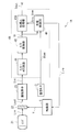
- FIG. 1 is a block diagram illustrating a schematic configuration example of an imaging apparatus according to a first embodiment of the present disclosure. It is sectional drawing showing the structural example of the liquid crystal light control element as an example of the light control element shown in FIG.
- FIG. 2 is a block diagram illustrating a detailed configuration example of a color correction processing unit illustrated in FIG. 1.
- FIG. 3 is a schematic diagram illustrating an example of a relationship between a driving voltage and a light transmittance of incident light in the liquid crystal light adjusting device illustrated in FIG. 2. It is a characteristic view showing an example of the relationship between the wavelength and the transmittance
- FIG. 5 is a schematic diagram illustrating an example of a correction table illustrated in FIG. 4.
- FIG. 5 is a flowchart illustrating an example of color correction processing according to the first embodiment.
- FIG. 8 is a schematic diagram illustrating a calculation example of a color correction value in the color correction process illustrated in FIG. 7. It is a block diagram showing the schematic structural example of the imaging device which concerns on 2nd Embodiment.
- FIG. 10 is a block diagram illustrating a detailed configuration example of a color correction processing unit illustrated in FIG. 9. It is a schematic diagram showing an example of the correction table shown in FIG. It is a figure showing the detailed structural example of the correction table shown in FIG. It is a flowchart showing the example of a color correction process which concerns on 2nd Embodiment. It is a schematic diagram showing the example of calculation of the color correction value in the case of the color correction process shown in FIG. 10 is a block diagram illustrating a configuration example of a color correction processing unit according to Modifications 1 and 2.
- FIG. 10 is a block diagram illustrating a configuration example of a color correction processing unit according to Modifications 1
- FIG. 1 is a block diagram illustrating a schematic configuration of an imaging apparatus (imaging apparatus 1) according to the first embodiment of the present disclosure.
- the imaging device 1 is a digital camera (digital still camera) or the like that converts an optical image from a subject into an electrical signal by an imaging device (an imaging device 23 described later).
- the imaging signal (digital signal) obtained in this way can be recorded on a semiconductor recording medium (not shown) or displayed on a display device (not shown) such as a liquid crystal display. It has become.
- the imaging device 1 includes a lens 21, a light control element 22, an imaging element 23, a temperature sensor 3, a signal processing unit 4, and a driving unit 5.
- a color correction method according to an embodiment of the present disclosure is embodied in the imaging apparatus 1 (specifically, a color correction processing unit 43 described later) according to the present embodiment, and thus will be described below. . This also applies to other embodiments and modifications described later.
- the lens 21 is composed of one lens here, but may be composed of a lens group composed of a plurality of lenses.
- the light control element 22 is an element that adjusts the amount of imaging light (imaging light Lin) incident from the lens 21 side, and here, on the optical path between the lens 21 and the imaging element 23 (on the optical path of the imaging light). Has been placed.
- imaging light Lin imaging light
- the thing (liquid crystal light control element) etc. which adjust light quantity (light control) electrically using a liquid crystal etc. are mentioned, for example.
- the detailed configuration of such a liquid crystal light adjusting device will be described later (FIG. 2).
- the imaging element 23 is an element that detects imaging light (imaging light Lout emitted from the dimming element 22) incident from the lens 21 via the dimming element 22 and acquires an imaging signal Sin.
- the image sensor 23 is configured using an imaging sensor (solid-state image sensor) such as a CCD (Charge-Coupled Device) or a CMOS (Complementary Metal-Oxide Semiconductor).
- the temperature sensor 3 is disposed in the vicinity (peripheral region) of the light control element 22 and is an element for detecting the temperature in the vicinity of the light control element 22.
- the temperature sensor 3 is configured using, for example, a thermistor.
- the temperature information Item indicating the temperature in the vicinity of the light control element 22 detected in this way is output to the light quantity control unit 44.
- the signal processing unit 4 performs predetermined signal processing on the imaging signal Sin obtained by the imaging element 23 and performs predetermined feedback control (light amount control described later) on the dimming element 22.
- the signal processing unit 4 includes an S / H • AGC circuit 41, an A / D conversion unit 42, a color correction processing unit 43, and a light amount control unit (light transmittance control unit) 44.
- the S / H • AGC circuit 41 performs S / H (sample and hold) processing on the image signal Sin output from the image sensor 23 and predetermined signal amplification processing using an AGC (Automatic Gain Control) function. It is a circuit which performs.
- the A / D conversion unit 42 performs an A / D conversion (analog / digital conversion) process on the imaging signal output from the S / H • AGC circuit 41, thereby generating an imaging signal S1 including a digital signal. Is.
- the color correction processing unit 43 performs a color correction process as an image quality improvement process on the image pickup signal S1 (digital signal) output from the A / D conversion unit 42, whereby the image pickup signal after such a color correction process is performed. Sout is output.
- the color correction processing unit 43 performs color correction processing using temperature information Item supplied from the light amount control unit 44 and drive voltage information Iv described later. That is, by performing color correction processing using such drive voltage information Iv, color correction processing is performed indirectly using light transmittance information Itra (light amount information) described later.
- the image pickup signal Sout generated by such color correction processing is output to the outside of the signal processing unit 4 (a semiconductor recording medium (not shown) or the like).
- the detailed configuration of the color correction processing unit 43 will be described later (FIG. 3).
- the light amount control unit 44 controls the light control operation (light amount adjustment operation) of the light control element 22 by supplying a control signal of the light control element 22 to the drive unit 5.
- a control signal of the light control element 22 here, light transmittance information Itra (image light Lout (output from the light control element 22) indicating the light transmittance of the image light Lin (incident light) in the light control element 22 is used.
- Light amount information indicating the amount of light (emitted light) (transmitted light amount, brightness).
- the light amount control unit 44 detects a signal value in the imaging signal S1 output from the A / D conversion unit 42, and based on the signal value (detection value), the light transmittance information Itra (light amount information) ) Is set. That is, the light amount control unit 44 determines the light amount (transmitted light amount) of the imaging light Lout emitted from the light control element 22 based on the signal value of the imaging signal S1, and outputs information Itra regarding the light amount. Further, the light quantity control unit 44 uses temperature data output from the temperature sensor 3 using data (table) indicating “correspondence between temperature and transmitted light quantity” held in advance in a storage unit (memory) (not shown). It also has a function of performing predetermined temperature correction (temperature correction of transmitted light amount) using Item.
- the driving unit 5 performs a driving operation on the light control element 22 based on the light transmittance information Itra (light amount information) supplied from the light amount control unit 44. Specifically, the drive voltage V for the light control element 22 is determined based on such light transmittance information Itra, and the drive voltage V is determined with respect to the light control element 22 (between transparent electrodes 221a and 221b described later). By supplying, a driving operation is performed.
- information indicating the drive voltage V determined at this time corresponds to the drive voltage information Iv described above. The details of the method for determining the drive voltage V will be described later (FIG. 4).
- FIG. 2 schematically illustrates a cross-sectional configuration example of the light control element 22 (liquid crystal light control element).
- the dimming element 22 has a transparent substrate 221a, a transparent electrode 222a, an alignment film 223a, a liquid crystal layer 220, an alignment film 223b, a transparent electrode 222b, and a transparent substrate from the incident side of the imaging light Lin to the emission side of the imaging light Lout.
- the substrate 221b has a stacked structure in which the substrates are stacked in this order.
- the light control element 22 is also provided with a sealant 224, a spacer 225, and a sealing portion 226.
- the liquid crystal layer 220 is a layer containing liquid crystal molecules.
- the liquid crystal layer 220 contains predetermined dye molecules (dichroic dye molecules) in addition to the liquid crystal molecules (in order to simplify the illustration in FIG.
- the dye molecules are collectively shown as “molecule M”). That is, the light control element 22 is configured using a guest-host (GH) type liquid crystal containing a dye (dichroic dye).
- GH guest-host
- Such GH type liquid crystal is roughly classified into a negative type and a positive type depending on the difference in the major axis direction of liquid crystal molecules when a voltage is applied.
- the positive GH type liquid crystal when no voltage is applied (OFF state), the long axis direction of the liquid crystal molecules is perpendicular to the optical axis, and when the voltage is applied (ON state), the long axis direction of the liquid crystal molecules is light. It is parallel to the axis.
- the negative type GH liquid crystal the major axis direction of the liquid crystal molecules is parallel to the optical axis when no voltage is applied, and the major axis direction of the liquid crystal molecules is perpendicular to the optical axis when voltage is applied. Is.
- the dye molecules are aligned in the same direction (orientation) as the liquid crystal molecules, when positive type liquid crystal is used as a host, the light transmittance is relatively low when no voltage is applied (the light output side is relatively The light transmittance becomes relatively high when a voltage is applied (the light emission side becomes relatively bright).
- the light transmittance is relatively high when no voltage is applied (the light emission side is relatively bright), and the light transmittance is relative when a voltage is applied. (The light emission side becomes relatively dark).
- the liquid crystal layer 260 may be composed of either positive or negative liquid crystal, but a case where the liquid crystal layer 260 is made of negative liquid crystal will be described below as a representative. .
- the transparent electrodes 222a and 222b are electrodes for applying a voltage (drive voltage V) to the liquid crystal layer 220, and are made of, for example, indium tin oxide (ITO). Note that wirings (not shown) for electrical connection with the transparent electrodes 222a and 222b may be appropriately arranged.
- the alignment films 223a and 223b are films for aligning the liquid crystal molecules in the liquid crystal layer 220 in a desired direction (alignment direction).
- Each of these alignment films 223a and 223b is made of a polymer material such as polyimide, and the alignment direction of the liquid crystal molecules is set by performing a rubbing process in a predetermined direction in advance. .
- the transparent substrate 221a is a substrate on one side for supporting the transparent electrode 222a and the alignment film 223a and sealing the liquid crystal layer 220.
- the transparent substrate 221b is a substrate on the other side for supporting the transparent electrode 222b and the alignment film 223b and sealing the liquid crystal layer 220.
- Each of these transparent substrates 221a and 221b is made of a glass substrate, for example.
- the sealing agent 224 is a member for sealing the molecules M (liquid crystal molecules and dye molecules) in the liquid crystal layer 220 from the side surface, and is made of an adhesive such as an epoxy adhesive or an acrylic adhesive.
- the spacer 225 is a member for keeping the cell gap (thickness) in the liquid crystal layer 220 constant, and is made of, for example, a predetermined resin material or glass material.
- the sealing portion 226 is a sealing port when the molecules M are sealed in the liquid crystal layer 220 and is a portion for sealing the molecules M in the liquid crystal layer 220 from the outside after that.
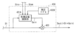
- FIG. 3 is a block diagram illustrating a detailed configuration example of the color correction processing unit 43.
- the color correction processing unit 43 includes a color correction value calculation unit 431, a correction table 432 (second correction table), and a multiplication unit 433.
- the color correction value calculation unit 431 uses the imaging signal S1, the drive voltage information Iv and temperature information Item supplied from the light amount control unit 44, and the correction table 432, and the color correction value Gain ( Gain value).
- This correction table 432 is a table in which the drive voltage information Iv and the color correction value Gain are associated with each other in advance, and in particular, in addition to these, temperature information Item is also associated. Such a correction table 432 is held in advance on a storage unit (memory) (not shown), for example. The detailed configuration of the correction table 432 will be described later (FIG. 6).
- Imaging operation In the imaging device 1, as shown in FIG. 1, the imaging light Lin emitted from the lens 21 enters the light control element 22, and the light amount (transmitted light amount) is adjusted and emitted as imaging light Lout. The imaging light Lout is incident on the imaging element 23 and detected, and an imaging signal Sin is obtained.
- the imaging light Lin (incident light) passes (transmits) through the liquid crystal layer 220 and the like, and is emitted as imaging light Lout (emitted light).
- a predetermined voltage driving voltage V
- the orientation direction major axis direction
- the molecules M liquid crystal molecules and dye molecules
- the light amount of the imaging light Lout (light transmittance of the imaging light Lin) passing through the entire light control element 22 can be adjusted electrically (not mechanically). (Arbitrary dimming operation is possible). In this manner, the light amount adjustment (light control) for the imaging light is performed in the light control element 22.
- FIG. 4 schematically shows an example of the relationship between the applied drive voltage V and the transmittance of the imaging light Lin (light transmittance T) in the light control device 22 (liquid crystal light control device).
- negative GH type liquid crystal is used in the liquid crystal layer 220, and the light amount (transmitted light amount) of the imaging light Lout in the voltage non-application state (OFF state) is shown as a reference (100%).
- the drive voltage V increases, the light shielding amount in the liquid crystal layer 220 increases rapidly (the light transmittance T decreases rapidly) and converges to a substantially constant value. It can be seen (ON state).
- the value, inclination, and dimming range when the light transmittance T in such a dimming element 22 is changed are the material and concentration of the liquid crystal layer 220 (liquid crystal and pigment), the cell gap (thickness) of the liquid crystal layer 220, It changes depending on the type (material) of the alignment films 223a and 223b.
- the transmittance is low when no voltage is applied and the light transmission is increased as the drive voltage V increases, contrary to the characteristics of FIG.
- the rate T tends to increase.
- the signal processing unit 4 performs predetermined signal processing on the imaging signal Sin obtained as described above, and performs predetermined feedback control (light amount control) on the dimming element 22.
- the S / H • AGC circuit 41 performs S / H processing on the imaging signal Sin and performs predetermined signal amplification processing using the AGC function.
- the A / D conversion unit 42 performs an A / D conversion process, thereby generating an imaging signal S1 including a digital signal.
- the color correction processing unit 43 performs a later-described color correction process on the imaging signal S1, and generates an imaging signal Sout after the color correction process.
- the light quantity control unit 44 in the signal processing unit 4 uses the signal value (detection value) in the imaging signal S1 and the temperature information Item (temperature information in the vicinity of the light control element 22) output from the temperature sensor 3.
- the light transmittance information Itra (light quantity information) as a control signal for the light control element 22 is set and output.
- the drive unit 5 performs a drive operation on the light control element 22 based on the light transmittance information Itra supplied from the light amount control unit 44.
- the drive voltage V of the light control element 22 is determined based on such light transmittance information Itra, and the drive voltage V is supplied to the light control element 22 (between the transparent electrodes 221a and 221b).
- a driving operation is performed.
- the drive unit 5 uses the characteristic line (for example, see FIG. 4 described above) indicating the relationship between the light transmittance T and the drive voltage V in the light control element 22 to obtain the drive voltage V from the light transmittance information Itra. decide.
- the imaging is performed according to the wavelength region of the imaging light
- the light transmittance is slightly different.
- the light transmittance for each wavelength region does not change uniformly according to a change in temperature (environment temperature near the dimming element).
- the light transmittance decreases as the temperature increases from a low temperature to a high temperature, whereas red (R).
- the wavelength region the light transmittance increases conversely as the temperature increases from a low temperature to a high temperature.
- the color of the imaging light transmitted through the light control element changes according to the transmitted light amount (brightness) and temperature of the imaging light at that time, and the color balance (white balance) in the imaging signal is eventually changed. It will change. Note that such a color balance shift in the image pickup signal is conspicuous in the case of a liquid crystal light control device.
- the color correction processing unit 43 in the signal processing unit 4 performs the following with respect to the imaging signal obtained through the dimming element 22 (here, the imaging signal S1 after the subsequent signal processing). By performing the color correction processing to be described, the above-described color balance deviation is reduced.
- the color correction processing unit 43 indirectly transmits information (light transmittance information Itra) regarding the light amount (transmitted light amount) of the imaging light Lout emitted from the light control element 22.
- the color correction processing is performed on the imaging signal S1. Specifically, using drive voltage information Iv (information indicating the drive voltage V of the light control element 22) and temperature information Item (information indicating the temperature in the vicinity of the light control element 22) supplied from the light quantity control unit 44, Such color correction processing is performed. More specifically, color correction processing is performed using a correction table 432 in which drive voltage information Iv and color correction value Gain are associated in advance.
- the value of the drive voltage information Iv and the color correction value Gain (for example, the color correction value R_Gain for red and the color correction value B_Gain for blue).
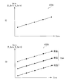
- the value of the drive voltage information Iv and the color correction value Gain are associated with each other by the predetermined characteristic line for each value of the temperature information Item (low temperature, normal temperature, high temperature, etc.).
- the relationship between the drive voltage V and the light transmittance T in the light control element 22 (liquid crystal light control element) is generally defined by, for example, a characteristic curve composed of a cubic equation.
- the characteristic line defining the correspondence in the correction table 432 is also a characteristic curve composed of a cubic equation.
- the correction formula that defines the association in the correction table 432 is a cubic formula here.
- the color correction processing unit 43 uses the color correction value Gain obtained from the correction table 432 as described above, so that the color balance value in the imaging signal Sout is adjusted with the light amount of the imaging light Lout emitted from the dimming element 22.
- Color correction processing is performed so as to be substantially constant (preferably constant) without depending on both the temperature in the vicinity of the optical element 22.
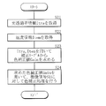
- the color correction processing unit 43 performs color correction processing as shown in FIG. 7, for example.
- the color correction processing unit 43 acquires the drive voltage information Iv and the temperature information Item from the light amount control unit 44 (steps S11 and S12 in FIG. 7). Next, the color correction processing unit 43 obtains the color correction value Gain from the correction table 432 described above using the drive voltage information Iv and the temperature information Item acquired in this manner (step S13).
- the cubic equation (approximate equation) in the correction table 432 at this time is, for example, the following equations (1) and (2). It should be noted that the coefficients a R , b R , c R , d R , a B , b B , c B , and d B in these equations are held in the correction table 432, respectively. In this way, first, the color correction value Gain by the drive voltage V is obtained.
- Rx a R ⁇ Vx 3 + b R ⁇ Vx 2 + c R ⁇ Vx + d R (1)
- Bx a B ⁇ Vx 3 + b B ⁇ Vx 2 + c B ⁇ Vx + d B (2)
- the color correction processing unit 43 obtains a color correction value Gain in consideration of the temperature indicated by the temperature information Item (the temperature in the vicinity of the light control element 22). This is because, as shown in FIG. 6B, the color correction value Gain differs depending on the temperature even if the drive voltage V is the same. However, as shown in FIG. 8B, for example, since there is a linear relationship between the temperature and the color correction value Gain, for example, a high temperature (here 70 ° C.) and a low temperature (here ⁇ 10 ° C.) The color correction values Gain are held in the correction table 432 only at two places.
- R (T X ) R (T ⁇ 10 ) + ⁇ ⁇ ⁇ R (T 70 ) ⁇ R (T ⁇ 10 ) ⁇ (3)
- B (T X ) B (T ⁇ 10 ) + ⁇ ⁇ ⁇ B (T 70 ) ⁇ B (T ⁇ 10 ) ⁇ (4)
- ⁇ [Tx / ⁇ 70 ⁇ ( ⁇ 10) ⁇ ] (5)
- color correction processing realizes color correction in consideration of information (light transmittance information Itra) regarding the amount of imaging light Lout emitted from the light control element 22.
- color correction is performed in consideration of temperature information (temperature information Item) in the vicinity of the light control element 22 in addition to information on the light amount (light transmittance information Itra).
- the dimming element 22 is used. Since the color correction processing is performed on the imaging signal S1 obtained through the above method, it is possible to realize color correction in consideration of such information regarding the amount of light. Therefore, it is possible to perform appropriate color correction on the imaging signal acquired using the light control element 22.
- color correction processing is performed using temperature information Item indicating the temperature in the vicinity of the light control element 22 in addition to the information on the light amount (light transmittance information Itra). Color reproduction including characteristics can be realized.
- FIG. 9 is a block diagram illustrating a schematic configuration of an imaging apparatus (imaging apparatus 1A) according to the second embodiment of the present disclosure.
- This imaging device 1A includes the signal processing unit 4A instead of the signal processing unit 4 in the imaging device 1 of the first embodiment, and other configurations are the same.
- the same components as those in the first embodiment are denoted by the same reference numerals, and description thereof will be omitted as appropriate.
- the signal processing unit 4A is provided with a color correction processing unit 43A instead of the color correction processing unit 43 in the signal processing unit 4 in the first embodiment, and other configurations are the same.
- the color correction processing unit 43A performs color correction processing using temperature information Item and light transmittance information Itra (light amount information) supplied from the light amount control unit 44. . That is, the color correction processing unit 43 performs color correction processing indirectly using information (light transmittance information Itra) regarding the light amount of the imaging light Lout, whereas the color correction processing unit 43A performs such a color correction processing. Color correction processing is performed by directly using information relating to the light amount of the imaging light Lout.
- the color correction processing unit 43A includes, for example, a color correction value calculation unit 431A, a correction table 432A, and a multiplication unit 433 as illustrated in FIG. That is, in the color correction processing unit 43, a color correction value calculation unit 431A and a correction table 432A (first correction table) are provided instead of the color correction value calculation unit 431 and the correction table 432, respectively.
- the color correction value calculation unit 431A uses the imaging signal S1, the light transmittance information Itra and the temperature information Item supplied from the light amount control unit 44, and the correction table 432A, and the color correction value Gain at the time of color correction processing. Is what you want.
- the correction table 432A is a table in which the light transmittance information Itra and the color correction value Gain are associated with each other in advance, and here, in particular, the temperature information Item is also associated with them. Such a correction table 432A is also held in advance on a storage unit (memory) (not shown), for example.
- a correction table 432A for example, as shown in FIG. 11A, the value of the light transmittance information Itra and the color correction value Gain (for example, the color correction value R_Gain for red, the color correction for blue). Value B_Gain) is associated with a predetermined characteristic line.
- the value of the light transmittance information Itra and the color correction value Gain correspond to each value of the temperature information Item (low temperature, normal temperature, high temperature, etc.) by a predetermined characteristic line. The ones attached are listed.
- the characteristic line that defines the correspondence in the correction table 432A is 1 because it is performed using the light transmittance information Itra directly as described above. It is a characteristic line consisting of the following formula.
- the correction formula that defines the association in the correction table 432A is a primary formula here. That is, the value of the light transmittance information Itra and the color correction value Gain have a linear relationship.
- the correction equation is a complex expression such as a cubic equation
- the correction equation is a linear equation. Therefore, a simpler and more accurate color correction process than that of the first embodiment is realized.
- a part of the color correction value Gain positioned on the correction equation can be interpolated and generated by linear interpolation (linear function interpolation). is there.
- linear interpolation linear function interpolation
- the interpolation may be generated by linear interpolation. In that case, the configuration of the correction table 432A becomes simpler (the data capacity is smaller).
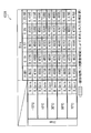
- FIG. 12 shows an example of such a correction table 432A more specifically.
- the value of the light transmittance information Itra (specified by the light transmittance ratio when the darkest state is used as a reference) and the color correction value Gain (red color correction value R_Gain, blue color correction value B_Gain) are associated with each value ( ⁇ 10 ° C. to 70 ° C.) of the temperature information Item.
- the same color correction processing as that of the first embodiment is performed using the color correction value Gain obtained from the correction table 432A. That is, the color balance value in the imaging signal Sout is substantially constant (preferably constant) without depending on both the light amount of the imaging light Lout emitted from the dimmer 22 and the temperature in the vicinity of the dimmer 22.
- color correction processing is performed. Specifically, in the present embodiment, the color correction processing unit 43A performs color correction processing as shown in FIG. 13, for example.
- the color correction processing unit 43A acquires the light transmittance information Itra and the temperature information Item from the light amount control unit 44 as described above (steps S21 and S22 in FIG. 13). Next, the color correction processing unit 43A obtains the color correction value Gain from the correction table 432A described above using the light transmittance information Itra and the temperature information Item acquired in this way (step S23).
- the color correction processing unit 43A holds only the coordinates of the two points P0 and P1 shown in FIG. 14, for example, in the correction table 432A.
- To (8) are used to determine the coordinates of the point Px that defines the color correction value Gain. In this way, first, the color correction value Gain based on the light transmittance is obtained.
- Rx R0 + a ⁇ (R1-R0) (6)
- Bx B0 + a ⁇ (B1-B0) (7)
- a (Ex / 1.33)
- the color correction processing unit 43A obtains a color correction value Gain in consideration of the temperature indicated by the temperature information Item (the temperature in the vicinity of the dimming element 22), similarly to step S13 described in the first embodiment. .
- the color correction processing is performed by directly using the information regarding the light amount of the imaging light Lout, so that the correction formula in the correction table 432A is a linear formula, and the first Compared with the present embodiment, a simple and accurate color correction process can be realized.
- FIG. 15A illustrates a block configuration of a color correction processing unit (color correction processing unit 43B) according to the first modification.
- FIG. 15B illustrates a block configuration of a color correction processing unit (color correction processing unit 43C) according to Modification 2.
- the color correction processing unit 43B according to Modification 1 is provided with a color correction value calculation unit 431B instead of the color correction value calculation unit 431 in the color correction processing unit 43 according to the first embodiment. Is the same.
- the color correction value calculation unit 431B does not use the temperature information Item supplied from the light amount control unit 44, but the drive voltage supplied from the light amount control unit 44. Color correction processing is performed using the information Iv. Therefore, in this modification, for example, the correction table 432 shown in FIG. 6A is used.
- the color correction processing unit 43C according to the modification 2 is obtained by providing a color correction value calculation unit 431C instead of the color correction value calculation unit 431A in the color correction processing unit 43A according to the second embodiment. Is the same.
- the color correction processing unit 43C differs from the color correction processing unit 43A in that the color correction value calculation unit 431C does not use the temperature information Item supplied from the light amount control unit 44 and transmits light transmitted from the light amount control unit 44. Color correction processing is performed using rate information Itra (light quantity information). Therefore, in this modification, for example, the correction table 432A shown in FIG. 11A is used.
- the color information is directly or indirectly used without using the temperature information Item supplied from the light quantity control unit 44 and using the information (light transmittance information Itra) regarding the light quantity of the imaging light Lout. Correction processing may be performed.
- the color balance value in the imaging signal Sout is substantially constant (preferably constant) without depending on the light amount of the imaging light Lout emitted from the light control element 22. Perform color correction processing.
- a liquid crystal light control element using a GH type liquid crystal has been described as an example.
- a dimming element other than a liquid crystal dimming element may be used.
- light control elements other than the liquid crystal light control elements include light control elements of the following method. That is, for example, thermochromism (practical examples: mugs, polymer sheets, etc.), dimmers using gel materials used for thermotropic, and photochromic (practical examples: sunglasses that change with ultraviolet rays, etc.) WO 3 (tungsten oxide), Nb 2 O 5 (niobium oxide) in a light control element using hydrogen gas or the like in an optical element, gas chromic (practical example: window glass, etc.), electrochromic (practical example: window glass, etc.) , NiO (nickel oxide), Cr 2 O 3 (chromium oxide), and the like.
- thermochromism (practical examples: mugs, polymer sheets, etc.), dimmers using gel materials used for thermotropic, and photochromic (practical examples: sunglasses that change with ultraviolet rays, etc.)
- WO 3 tungsten oxide
- Nb 2 O 5 niobium oxide
- gas chromic practical example: window
- each component (block configuration of the signal processing unit) of the imaging device has been specifically described, but it is not necessary to include all the components, and other components are not included. Furthermore, you may provide.
- the case where one lens (lens group) is provided in the imaging apparatus (on the optical path of the imaging light) has been described as an example, but the present invention is not limited thereto. That is, for example, a plurality of lenses (lens groups) may be provided on the optical path of the imaging light, or such lenses (lens groups) may not be provided in the imaging apparatus.
- the signal processing (color correction processing or the like) described in the above embodiments may be performed by hardware (circuit), or may be performed by software (program).
- the software includes a program group for causing each signal processing function (color correction processing function or the like) to be executed by a computer (such as a microcomputer in the imaging apparatus).
- Each program may be used by being incorporated in advance in dedicated hardware, for example, or installed in a general-purpose personal computer or the like from a network or a recording medium.
- this technique can also take the following structures.
- a light control element for adjusting the amount of incident imaging light;
- An image pickup device for acquiring an image pickup signal based on the image pickup light emitted from the light control device;
- a color correction processing unit that performs color correction on an imaging signal obtained by the imaging device based on information on the amount of imaging light emitted from the dimming device;
- the color correction processing unit performs the color correction so that a color balance value in the imaging signal becomes substantially constant without depending on the amount of imaging light emitted from the light control element.
- a light amount control unit that determines the light amount of the imaging light emitted from the light control element based on the signal value of the imaging signal, and outputs information on the light amount;
- a drive unit for determining a drive voltage for the light control element based on information on the light amount output from the light amount control unit, and supplying the drive voltage to the light control element;
- the imaging apparatus according to any one of (2) to (5), wherein the color correction processing unit acquires information on the light amount from the light amount control unit.
- the color correction processing unit performs the color correction by indirectly using information on the light amount.
- a light amount control unit that determines the light amount of the imaging light emitted from the light control element based on the signal value of the imaging signal, and outputs information on the light amount;
- a drive unit that determines the drive voltage based on information on the light amount output from the light amount control unit, and supplies the drive voltage to the dimming element; and
- the imaging apparatus according to (8) or (9), wherein the color correction processing unit acquires the driving voltage information from the driving unit via the light amount control unit.
- (11) The imaging according to any one of (1) to (10), wherein the color correction processing unit performs the color correction by using temperature information indicating a temperature in the vicinity of the light control element in addition to the information on the light amount. apparatus.
- the color correction processing unit is configured so that a color balance value in the imaging signal is substantially constant without depending on both the amount of imaging light emitted from the light control element and the temperature in the vicinity of the light control element.
- the information regarding the light amount is information indicating light transmittance in the light control element.
Landscapes
- Engineering & Computer Science (AREA)
- Multimedia (AREA)
- Signal Processing (AREA)
- Physics & Mathematics (AREA)
- General Physics & Mathematics (AREA)
- Color Television Image Signal Generators (AREA)
- Studio Devices (AREA)
- Liquid Crystal (AREA)
Priority Applications (6)
| Application Number | Priority Date | Filing Date | Title |
|---|---|---|---|
| US14/354,734 US9398281B2 (en) | 2011-12-02 | 2012-11-13 | Image pickup apparatus, color correction method, and color correction program |
| RU2014121227/07A RU2014121227A (ru) | 2011-12-02 | 2012-11-13 | Устройство съемки изображения, способ коррекции цвета и программа коррекции цвета |
| EP12852756.1A EP2787730A4 (en) | 2011-12-02 | 2012-11-13 | IMAGING DEVICE, COLOR CORRECTION METHOD, AND COLOR CORRECTION PROGRAM |
| IN980MUN2014 IN2014MN00980A (pt) | 2011-12-02 | 2012-11-13 | |
| CN201280057946.0A CN103975584B (zh) | 2011-12-02 | 2012-11-13 | 图像拾取设备和颜色校正方法 |
| BR112014012685A BR112014012685A8 (pt) | 2011-12-02 | 2012-11-13 | aparelho de captação de imagem, e, método e programa para correção de cor |
Applications Claiming Priority (2)
| Application Number | Priority Date | Filing Date | Title |
|---|---|---|---|
| JP2011264959A JP5834850B2 (ja) | 2011-12-02 | 2011-12-02 | 撮像装置、色補正方法および色補正プログラム |
| JP2011-264959 | 2011-12-02 |
Publications (1)
| Publication Number | Publication Date |
|---|---|
| WO2013080785A1 true WO2013080785A1 (ja) | 2013-06-06 |
Family
ID=48535252
Family Applications (1)
| Application Number | Title | Priority Date | Filing Date |
|---|---|---|---|
| PCT/JP2012/079390 WO2013080785A1 (ja) | 2011-12-02 | 2012-11-13 | 撮像装置、色補正方法および色補正プログラム |
Country Status (8)
| Country | Link |
|---|---|
| US (1) | US9398281B2 (pt) |
| EP (1) | EP2787730A4 (pt) |
| JP (1) | JP5834850B2 (pt) |
| CN (1) | CN103975584B (pt) |
| BR (1) | BR112014012685A8 (pt) |
| IN (1) | IN2014MN00980A (pt) |
| RU (1) | RU2014121227A (pt) |
| WO (1) | WO2013080785A1 (pt) |
Families Citing this family (3)
| Publication number | Priority date | Publication date | Assignee | Title |
|---|---|---|---|---|
| KR102481355B1 (ko) * | 2015-09-30 | 2022-12-27 | 다이니폰 인사츠 가부시키가이샤 | 조광 셀 |
| WO2017203929A1 (ja) * | 2016-05-25 | 2017-11-30 | シャープ株式会社 | 調光装置 |
| JP6936650B2 (ja) * | 2017-07-27 | 2021-09-22 | 三菱パワー株式会社 | モデル学習装置、学習済みモデルの生成方法、プログラム、学習済みモデル、監視装置、および監視方法 |
Citations (5)
| Publication number | Priority date | Publication date | Assignee | Title |
|---|---|---|---|---|
| JPH0654253A (ja) * | 1992-07-30 | 1994-02-25 | Canon Inc | カメラ |
| JPH0678208A (ja) * | 1992-08-24 | 1994-03-18 | Canon Inc | ビデオカメラ |
| JPH1032832A (ja) * | 1996-07-17 | 1998-02-03 | Canon Inc | ビデオカメラ |
| JP2001142050A (ja) | 1999-11-12 | 2001-05-25 | Sony Corp | 調光装置及び撮像装置、並びにこれらの駆動方法 |
| JP2011017819A (ja) * | 2009-07-08 | 2011-01-27 | Sony Corp | 撮像光学系及び撮像装置 |
Family Cites Families (4)
| Publication number | Priority date | Publication date | Assignee | Title |
|---|---|---|---|---|
| US6952233B2 (en) * | 1992-07-23 | 2005-10-04 | Canon Kabushiki Kaisha | Video camera having a material element for controlling light transmission |
| JP3922238B2 (ja) * | 2003-10-22 | 2007-05-30 | ソニー株式会社 | 光量制御装置およびカメラ装置 |
| JP4333478B2 (ja) * | 2004-05-27 | 2009-09-16 | 株式会社ニコン | 撮像装置および画像処理プログラム |
| JP4438696B2 (ja) * | 2005-06-15 | 2010-03-24 | セイコーエプソン株式会社 | 画像表示装置及び方法 |
-
2011
- 2011-12-02 JP JP2011264959A patent/JP5834850B2/ja active Active
-
2012
- 2012-11-13 BR BR112014012685A patent/BR112014012685A8/pt not_active Application Discontinuation
- 2012-11-13 RU RU2014121227/07A patent/RU2014121227A/ru not_active Application Discontinuation
- 2012-11-13 EP EP12852756.1A patent/EP2787730A4/en not_active Withdrawn
- 2012-11-13 WO PCT/JP2012/079390 patent/WO2013080785A1/ja active Application Filing
- 2012-11-13 IN IN980MUN2014 patent/IN2014MN00980A/en unknown
- 2012-11-13 US US14/354,734 patent/US9398281B2/en active Active
- 2012-11-13 CN CN201280057946.0A patent/CN103975584B/zh active Active
Patent Citations (5)
| Publication number | Priority date | Publication date | Assignee | Title |
|---|---|---|---|---|
| JPH0654253A (ja) * | 1992-07-30 | 1994-02-25 | Canon Inc | カメラ |
| JPH0678208A (ja) * | 1992-08-24 | 1994-03-18 | Canon Inc | ビデオカメラ |
| JPH1032832A (ja) * | 1996-07-17 | 1998-02-03 | Canon Inc | ビデオカメラ |
| JP2001142050A (ja) | 1999-11-12 | 2001-05-25 | Sony Corp | 調光装置及び撮像装置、並びにこれらの駆動方法 |
| JP2011017819A (ja) * | 2009-07-08 | 2011-01-27 | Sony Corp | 撮像光学系及び撮像装置 |
Non-Patent Citations (1)
| Title |
|---|
| See also references of EP2787730A4 |
Also Published As
| Publication number | Publication date |
|---|---|
| BR112014012685A2 (pt) | 2017-06-13 |
| EP2787730A4 (en) | 2015-11-18 |
| CN103975584A (zh) | 2014-08-06 |
| CN103975584B (zh) | 2016-08-24 |
| IN2014MN00980A (pt) | 2015-04-24 |
| EP2787730A1 (en) | 2014-10-08 |
| US20140300772A1 (en) | 2014-10-09 |
| BR112014012685A8 (pt) | 2017-06-20 |
| US9398281B2 (en) | 2016-07-19 |
| JP5834850B2 (ja) | 2015-12-24 |
| RU2014121227A (ru) | 2015-12-10 |
| JP2013118503A (ja) | 2013-06-13 |
Similar Documents
| Publication | Publication Date | Title |
|---|---|---|
| JP2013150167A (ja) | 撮像装置、色補正方法、および色補正プログラム | |
| US8659722B2 (en) | Optical device and imaging device | |
| JP6198235B2 (ja) | 撮像装置 | |
| JP3201801B2 (ja) | 投影表示装置 | |
| JP2013114030A (ja) | 液晶調光装置、撮像装置および液晶調光素子の駆動方法 | |
| US20060279502A1 (en) | Method for fabricating liquid crystal display panel | |
| JP6838203B2 (ja) | 液晶ディスプレイパネルのグレースケール補正データの検出方法 | |
| US11665436B2 (en) | Imaging device and camera system | |
| WO2019085667A1 (zh) | 一种显示装置和显示驱动方法 | |
| EP4170417A1 (en) | Display device and display optimization method | |
| JP5834850B2 (ja) | 撮像装置、色補正方法および色補正プログラム | |
| WO2012056978A1 (ja) | 撮像装置 | |
| WO2021253495A1 (zh) | 显示装置及显示优化方法 | |
| JP2011209514A (ja) | 画像表示装置および画像表示方法 | |
| JP2007081544A (ja) | 撮影装置 | |
| JP2009224993A (ja) | 差動インタフェース装置、表示制御装置、及び表示装置 | |
| JP6693528B2 (ja) | 調光駆動装置、撮像装置、調光駆動方法 | |
| JP2007104419A (ja) | 撮影装置 | |
| TWI272420B (en) | Display device | |
| JP5002665B2 (ja) | 液晶表示装置 | |
| JP2007094083A (ja) | 撮影装置 | |
| JP2004004548A (ja) | 反応及び先行スルーレート制限によるスパークル低減方法及び装置 | |
| JP2021076821A (ja) | 液晶表示装置 | |
| JP2004109572A (ja) | 液晶表示装置 | |
| JP2006119205A (ja) | 液晶表示装置及びその黒電圧の設定方法 |
Legal Events
| Date | Code | Title | Description |
|---|---|---|---|
| 121 | Ep: the epo has been informed by wipo that ep was designated in this application |
Ref document number: 12852756 Country of ref document: EP Kind code of ref document: A1 |
|
| WWE | Wipo information: entry into national phase |
Ref document number: 14354734 Country of ref document: US |
|
| ENP | Entry into the national phase |
Ref document number: 2014121227 Country of ref document: RU Kind code of ref document: A |
|
| NENP | Non-entry into the national phase |
Ref country code: DE |
|
| REG | Reference to national code |
Ref country code: BR Ref legal event code: B01A Ref document number: 112014012685 Country of ref document: BR |
|
| ENP | Entry into the national phase |
Ref document number: 112014012685 Country of ref document: BR Kind code of ref document: A2 Effective date: 20140526 |