WO2013080785A1 - Imaging device, colour-correction method and colour-correction program - Google Patents
Imaging device, colour-correction method and colour-correction program Download PDFInfo
- Publication number
- WO2013080785A1 WO2013080785A1 PCT/JP2012/079390 JP2012079390W WO2013080785A1 WO 2013080785 A1 WO2013080785 A1 WO 2013080785A1 JP 2012079390 W JP2012079390 W JP 2012079390W WO 2013080785 A1 WO2013080785 A1 WO 2013080785A1
- Authority
- WO
- WIPO (PCT)
- Prior art keywords
- light
- color correction
- imaging
- amount
- information
- Prior art date
Links
Images


Classifications
-
- H—ELECTRICITY
- H04—ELECTRIC COMMUNICATION TECHNIQUE
- H04N—PICTORIAL COMMUNICATION, e.g. TELEVISION
- H04N9/00—Details of colour television systems
- H04N9/64—Circuits for processing colour signals
- H04N9/73—Colour balance circuits, e.g. white balance circuits or colour temperature control
-
- G—PHYSICS
- G03—PHOTOGRAPHY; CINEMATOGRAPHY; ANALOGOUS TECHNIQUES USING WAVES OTHER THAN OPTICAL WAVES; ELECTROGRAPHY; HOLOGRAPHY
- G03B—APPARATUS OR ARRANGEMENTS FOR TAKING PHOTOGRAPHS OR FOR PROJECTING OR VIEWING THEM; APPARATUS OR ARRANGEMENTS EMPLOYING ANALOGOUS TECHNIQUES USING WAVES OTHER THAN OPTICAL WAVES; ACCESSORIES THEREFOR
- G03B7/00—Control of exposure by setting shutters, diaphragms or filters, separately or conjointly
- G03B7/22—Control of exposure by setting shutters, diaphragms or filters, separately or conjointly in accordance with temperature or height, e.g. in aircraft
-
- G—PHYSICS
- G03—PHOTOGRAPHY; CINEMATOGRAPHY; ANALOGOUS TECHNIQUES USING WAVES OTHER THAN OPTICAL WAVES; ELECTROGRAPHY; HOLOGRAPHY
- G03B—APPARATUS OR ARRANGEMENTS FOR TAKING PHOTOGRAPHS OR FOR PROJECTING OR VIEWING THEM; APPARATUS OR ARRANGEMENTS EMPLOYING ANALOGOUS TECHNIQUES USING WAVES OTHER THAN OPTICAL WAVES; ACCESSORIES THEREFOR
- G03B7/00—Control of exposure by setting shutters, diaphragms or filters, separately or conjointly
- G03B7/18—Control of exposure by setting shutters, diaphragms or filters, separately or conjointly in accordance with light-reducing "factor" of filter or other obturator used with or on the lens of the camera
-
- G—PHYSICS
- G03—PHOTOGRAPHY; CINEMATOGRAPHY; ANALOGOUS TECHNIQUES USING WAVES OTHER THAN OPTICAL WAVES; ELECTROGRAPHY; HOLOGRAPHY
- G03B—APPARATUS OR ARRANGEMENTS FOR TAKING PHOTOGRAPHS OR FOR PROJECTING OR VIEWING THEM; APPARATUS OR ARRANGEMENTS EMPLOYING ANALOGOUS TECHNIQUES USING WAVES OTHER THAN OPTICAL WAVES; ACCESSORIES THEREFOR
- G03B9/00—Exposure-making shutters; Diaphragms
- G03B9/02—Diaphragms
-
- H—ELECTRICITY
- H04—ELECTRIC COMMUNICATION TECHNIQUE
- H04N—PICTORIAL COMMUNICATION, e.g. TELEVISION
- H04N23/00—Cameras or camera modules comprising electronic image sensors; Control thereof
- H04N23/10—Cameras or camera modules comprising electronic image sensors; Control thereof for generating image signals from different wavelengths
- H04N23/12—Cameras or camera modules comprising electronic image sensors; Control thereof for generating image signals from different wavelengths with one sensor only
-
- H—ELECTRICITY
- H04—ELECTRIC COMMUNICATION TECHNIQUE
- H04N—PICTORIAL COMMUNICATION, e.g. TELEVISION
- H04N23/00—Cameras or camera modules comprising electronic image sensors; Control thereof
- H04N23/70—Circuitry for compensating brightness variation in the scene
- H04N23/75—Circuitry for compensating brightness variation in the scene by influencing optical camera components
-
- H—ELECTRICITY
- H04—ELECTRIC COMMUNICATION TECHNIQUE
- H04N—PICTORIAL COMMUNICATION, e.g. TELEVISION
- H04N23/00—Cameras or camera modules comprising electronic image sensors; Control thereof
- H04N23/80—Camera processing pipelines; Components thereof
- H04N23/81—Camera processing pipelines; Components thereof for suppressing or minimising disturbance in the image signal generation
-
- H—ELECTRICITY
- H04—ELECTRIC COMMUNICATION TECHNIQUE
- H04N—PICTORIAL COMMUNICATION, e.g. TELEVISION
- H04N23/00—Cameras or camera modules comprising electronic image sensors; Control thereof
- H04N23/80—Camera processing pipelines; Components thereof
- H04N23/84—Camera processing pipelines; Components thereof for processing colour signals
- H04N23/843—Demosaicing, e.g. interpolating colour pixel values
-
- H—ELECTRICITY
- H04—ELECTRIC COMMUNICATION TECHNIQUE
- H04N—PICTORIAL COMMUNICATION, e.g. TELEVISION
- H04N23/00—Cameras or camera modules comprising electronic image sensors; Control thereof
- H04N23/80—Camera processing pipelines; Components thereof
- H04N23/84—Camera processing pipelines; Components thereof for processing colour signals
- H04N23/88—Camera processing pipelines; Components thereof for processing colour signals for colour balance, e.g. white-balance circuits or colour temperature control
-
- G—PHYSICS
- G02—OPTICS
- G02B—OPTICAL ELEMENTS, SYSTEMS OR APPARATUS
- G02B26/00—Optical devices or arrangements for the control of light using movable or deformable optical elements
- G02B26/02—Optical devices or arrangements for the control of light using movable or deformable optical elements for controlling the intensity of light
Definitions
- the present disclosure relates to an imaging apparatus that acquires an imaging signal using a dimming element, and a color correction method and a color correction program applied to such an imaging signal.
- a diaphragm (iris) that mechanically performs a dimming operation is usually provided as a dimming element that adjusts the light amount of imaging light.
- electrical dimmers liquid crystal dimmers
- GH guest-host
- an imaging signal is acquired by the imaging element via such a dimming element. Since it is assumed that the image signal obtained in this way may require color correction depending on the situation, a proposal of a method for realizing appropriate color correction is desired.
- An imaging device includes a dimming element that adjusts the amount of incident imaging light, an imaging element that acquires an imaging signal based on imaging light emitted from the dimming element, and dimming And a color correction processing unit configured to perform color correction on an image pickup signal obtained by the image pickup element based on information on the amount of image pickup light emitted from the element.
- the color correction processing unit performs color correction so that the color balance value in the imaging signal is substantially constant without depending on the amount of imaging light emitted from the light control element.
- a color correction method includes a step of acquiring an imaging signal in an imaging device based on imaging light emitted from a dimming device that adjusts the amount of incident imaging light; And a step of performing color correction on an image pickup signal obtained by the image pickup device based on information on the quantity of emitted image pickup light. In this color correction step, the color correction is performed so that the color balance value in the imaging signal becomes substantially constant without depending on the amount of imaging light emitted from the light control element.
- a color correction program includes a step of obtaining an imaging signal obtained by an imaging device based on imaging light emitted from a dimming device that adjusts the amount of incident imaging light;
- the computer is caused to execute a step of performing color correction on the imaging signal based on information on the amount of imaging light emitted from the element.
- the color correction is performed so that the color balance value in the imaging signal becomes substantially constant without depending on the amount of imaging light emitted from the light control element.
- the color balance value in the imaging signal obtained by the imaging element is based on the information regarding the amount of imaging light emitted from the dimming element. Then, the color correction is performed on the imaging signal so as to be substantially constant without depending on the amount of imaging light emitted from the light control element. That is, color correction considering information regarding the amount of imaging light emitted from the light control element is realized.
- color correction is performed on an imaging signal obtained by the imaging device based on information on the amount of imaging light emitted from the dimming device. Therefore, it is possible to realize color correction in consideration of such information on the amount of light. Therefore, it is possible to perform appropriate color correction on the imaging signal acquired using the light control element.
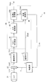
- FIG. 1 is a block diagram illustrating a schematic configuration example of an imaging apparatus according to a first embodiment of the present disclosure. It is sectional drawing showing the structural example of the liquid crystal light control element as an example of the light control element shown in FIG.
- FIG. 2 is a block diagram illustrating a detailed configuration example of a color correction processing unit illustrated in FIG. 1.
- FIG. 3 is a schematic diagram illustrating an example of a relationship between a driving voltage and a light transmittance of incident light in the liquid crystal light adjusting device illustrated in FIG. 2. It is a characteristic view showing an example of the relationship between the wavelength and the transmittance
- FIG. 5 is a schematic diagram illustrating an example of a correction table illustrated in FIG. 4.
- FIG. 5 is a flowchart illustrating an example of color correction processing according to the first embodiment.
- FIG. 8 is a schematic diagram illustrating a calculation example of a color correction value in the color correction process illustrated in FIG. 7. It is a block diagram showing the schematic structural example of the imaging device which concerns on 2nd Embodiment.
- FIG. 10 is a block diagram illustrating a detailed configuration example of a color correction processing unit illustrated in FIG. 9. It is a schematic diagram showing an example of the correction table shown in FIG. It is a figure showing the detailed structural example of the correction table shown in FIG. It is a flowchart showing the example of a color correction process which concerns on 2nd Embodiment. It is a schematic diagram showing the example of calculation of the color correction value in the case of the color correction process shown in FIG. 10 is a block diagram illustrating a configuration example of a color correction processing unit according to Modifications 1 and 2.
- FIG. 10 is a block diagram illustrating a configuration example of a color correction processing unit according to Modifications 1
- FIG. 1 is a block diagram illustrating a schematic configuration of an imaging apparatus (imaging apparatus 1) according to the first embodiment of the present disclosure.
- the imaging device 1 is a digital camera (digital still camera) or the like that converts an optical image from a subject into an electrical signal by an imaging device (an imaging device 23 described later).
- the imaging signal (digital signal) obtained in this way can be recorded on a semiconductor recording medium (not shown) or displayed on a display device (not shown) such as a liquid crystal display. It has become.
- the imaging device 1 includes a lens 21, a light control element 22, an imaging element 23, a temperature sensor 3, a signal processing unit 4, and a driving unit 5.
- a color correction method according to an embodiment of the present disclosure is embodied in the imaging apparatus 1 (specifically, a color correction processing unit 43 described later) according to the present embodiment, and thus will be described below. . This also applies to other embodiments and modifications described later.
- the lens 21 is composed of one lens here, but may be composed of a lens group composed of a plurality of lenses.
- the light control element 22 is an element that adjusts the amount of imaging light (imaging light Lin) incident from the lens 21 side, and here, on the optical path between the lens 21 and the imaging element 23 (on the optical path of the imaging light). Has been placed.
- imaging light Lin imaging light
- the thing (liquid crystal light control element) etc. which adjust light quantity (light control) electrically using a liquid crystal etc. are mentioned, for example.
- the detailed configuration of such a liquid crystal light adjusting device will be described later (FIG. 2).
- the imaging element 23 is an element that detects imaging light (imaging light Lout emitted from the dimming element 22) incident from the lens 21 via the dimming element 22 and acquires an imaging signal Sin.
- the image sensor 23 is configured using an imaging sensor (solid-state image sensor) such as a CCD (Charge-Coupled Device) or a CMOS (Complementary Metal-Oxide Semiconductor).
- the temperature sensor 3 is disposed in the vicinity (peripheral region) of the light control element 22 and is an element for detecting the temperature in the vicinity of the light control element 22.
- the temperature sensor 3 is configured using, for example, a thermistor.
- the temperature information Item indicating the temperature in the vicinity of the light control element 22 detected in this way is output to the light quantity control unit 44.
- the signal processing unit 4 performs predetermined signal processing on the imaging signal Sin obtained by the imaging element 23 and performs predetermined feedback control (light amount control described later) on the dimming element 22.
- the signal processing unit 4 includes an S / H • AGC circuit 41, an A / D conversion unit 42, a color correction processing unit 43, and a light amount control unit (light transmittance control unit) 44.
- the S / H • AGC circuit 41 performs S / H (sample and hold) processing on the image signal Sin output from the image sensor 23 and predetermined signal amplification processing using an AGC (Automatic Gain Control) function. It is a circuit which performs.
- the A / D conversion unit 42 performs an A / D conversion (analog / digital conversion) process on the imaging signal output from the S / H • AGC circuit 41, thereby generating an imaging signal S1 including a digital signal. Is.
- the color correction processing unit 43 performs a color correction process as an image quality improvement process on the image pickup signal S1 (digital signal) output from the A / D conversion unit 42, whereby the image pickup signal after such a color correction process is performed. Sout is output.
- the color correction processing unit 43 performs color correction processing using temperature information Item supplied from the light amount control unit 44 and drive voltage information Iv described later. That is, by performing color correction processing using such drive voltage information Iv, color correction processing is performed indirectly using light transmittance information Itra (light amount information) described later.
- the image pickup signal Sout generated by such color correction processing is output to the outside of the signal processing unit 4 (a semiconductor recording medium (not shown) or the like).
- the detailed configuration of the color correction processing unit 43 will be described later (FIG. 3).
- the light amount control unit 44 controls the light control operation (light amount adjustment operation) of the light control element 22 by supplying a control signal of the light control element 22 to the drive unit 5.
- a control signal of the light control element 22 here, light transmittance information Itra (image light Lout (output from the light control element 22) indicating the light transmittance of the image light Lin (incident light) in the light control element 22 is used.
- Light amount information indicating the amount of light (emitted light) (transmitted light amount, brightness).
- the light amount control unit 44 detects a signal value in the imaging signal S1 output from the A / D conversion unit 42, and based on the signal value (detection value), the light transmittance information Itra (light amount information) ) Is set. That is, the light amount control unit 44 determines the light amount (transmitted light amount) of the imaging light Lout emitted from the light control element 22 based on the signal value of the imaging signal S1, and outputs information Itra regarding the light amount. Further, the light quantity control unit 44 uses temperature data output from the temperature sensor 3 using data (table) indicating “correspondence between temperature and transmitted light quantity” held in advance in a storage unit (memory) (not shown). It also has a function of performing predetermined temperature correction (temperature correction of transmitted light amount) using Item.
- the driving unit 5 performs a driving operation on the light control element 22 based on the light transmittance information Itra (light amount information) supplied from the light amount control unit 44. Specifically, the drive voltage V for the light control element 22 is determined based on such light transmittance information Itra, and the drive voltage V is determined with respect to the light control element 22 (between transparent electrodes 221a and 221b described later). By supplying, a driving operation is performed.
- information indicating the drive voltage V determined at this time corresponds to the drive voltage information Iv described above. The details of the method for determining the drive voltage V will be described later (FIG. 4).
- FIG. 2 schematically illustrates a cross-sectional configuration example of the light control element 22 (liquid crystal light control element).
- the dimming element 22 has a transparent substrate 221a, a transparent electrode 222a, an alignment film 223a, a liquid crystal layer 220, an alignment film 223b, a transparent electrode 222b, and a transparent substrate from the incident side of the imaging light Lin to the emission side of the imaging light Lout.
- the substrate 221b has a stacked structure in which the substrates are stacked in this order.
- the light control element 22 is also provided with a sealant 224, a spacer 225, and a sealing portion 226.
- the liquid crystal layer 220 is a layer containing liquid crystal molecules.
- the liquid crystal layer 220 contains predetermined dye molecules (dichroic dye molecules) in addition to the liquid crystal molecules (in order to simplify the illustration in FIG.
- the dye molecules are collectively shown as “molecule M”). That is, the light control element 22 is configured using a guest-host (GH) type liquid crystal containing a dye (dichroic dye).
- GH guest-host
- Such GH type liquid crystal is roughly classified into a negative type and a positive type depending on the difference in the major axis direction of liquid crystal molecules when a voltage is applied.
- the positive GH type liquid crystal when no voltage is applied (OFF state), the long axis direction of the liquid crystal molecules is perpendicular to the optical axis, and when the voltage is applied (ON state), the long axis direction of the liquid crystal molecules is light. It is parallel to the axis.
- the negative type GH liquid crystal the major axis direction of the liquid crystal molecules is parallel to the optical axis when no voltage is applied, and the major axis direction of the liquid crystal molecules is perpendicular to the optical axis when voltage is applied. Is.
- the dye molecules are aligned in the same direction (orientation) as the liquid crystal molecules, when positive type liquid crystal is used as a host, the light transmittance is relatively low when no voltage is applied (the light output side is relatively The light transmittance becomes relatively high when a voltage is applied (the light emission side becomes relatively bright).
- the light transmittance is relatively high when no voltage is applied (the light emission side is relatively bright), and the light transmittance is relative when a voltage is applied. (The light emission side becomes relatively dark).
- the liquid crystal layer 260 may be composed of either positive or negative liquid crystal, but a case where the liquid crystal layer 260 is made of negative liquid crystal will be described below as a representative. .
- the transparent electrodes 222a and 222b are electrodes for applying a voltage (drive voltage V) to the liquid crystal layer 220, and are made of, for example, indium tin oxide (ITO). Note that wirings (not shown) for electrical connection with the transparent electrodes 222a and 222b may be appropriately arranged.
- the alignment films 223a and 223b are films for aligning the liquid crystal molecules in the liquid crystal layer 220 in a desired direction (alignment direction).
- Each of these alignment films 223a and 223b is made of a polymer material such as polyimide, and the alignment direction of the liquid crystal molecules is set by performing a rubbing process in a predetermined direction in advance. .
- the transparent substrate 221a is a substrate on one side for supporting the transparent electrode 222a and the alignment film 223a and sealing the liquid crystal layer 220.
- the transparent substrate 221b is a substrate on the other side for supporting the transparent electrode 222b and the alignment film 223b and sealing the liquid crystal layer 220.
- Each of these transparent substrates 221a and 221b is made of a glass substrate, for example.
- the sealing agent 224 is a member for sealing the molecules M (liquid crystal molecules and dye molecules) in the liquid crystal layer 220 from the side surface, and is made of an adhesive such as an epoxy adhesive or an acrylic adhesive.
- the spacer 225 is a member for keeping the cell gap (thickness) in the liquid crystal layer 220 constant, and is made of, for example, a predetermined resin material or glass material.
- the sealing portion 226 is a sealing port when the molecules M are sealed in the liquid crystal layer 220 and is a portion for sealing the molecules M in the liquid crystal layer 220 from the outside after that.
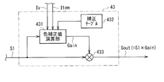
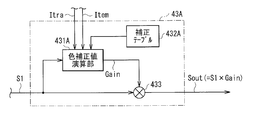
- FIG. 3 is a block diagram illustrating a detailed configuration example of the color correction processing unit 43.
- the color correction processing unit 43 includes a color correction value calculation unit 431, a correction table 432 (second correction table), and a multiplication unit 433.
- the color correction value calculation unit 431 uses the imaging signal S1, the drive voltage information Iv and temperature information Item supplied from the light amount control unit 44, and the correction table 432, and the color correction value Gain ( Gain value).
- This correction table 432 is a table in which the drive voltage information Iv and the color correction value Gain are associated with each other in advance, and in particular, in addition to these, temperature information Item is also associated. Such a correction table 432 is held in advance on a storage unit (memory) (not shown), for example. The detailed configuration of the correction table 432 will be described later (FIG. 6).
- Imaging operation In the imaging device 1, as shown in FIG. 1, the imaging light Lin emitted from the lens 21 enters the light control element 22, and the light amount (transmitted light amount) is adjusted and emitted as imaging light Lout. The imaging light Lout is incident on the imaging element 23 and detected, and an imaging signal Sin is obtained.
- the imaging light Lin (incident light) passes (transmits) through the liquid crystal layer 220 and the like, and is emitted as imaging light Lout (emitted light).
- a predetermined voltage driving voltage V
- the orientation direction major axis direction
- the molecules M liquid crystal molecules and dye molecules
- the light amount of the imaging light Lout (light transmittance of the imaging light Lin) passing through the entire light control element 22 can be adjusted electrically (not mechanically). (Arbitrary dimming operation is possible). In this manner, the light amount adjustment (light control) for the imaging light is performed in the light control element 22.
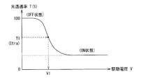
- FIG. 4 schematically shows an example of the relationship between the applied drive voltage V and the transmittance of the imaging light Lin (light transmittance T) in the light control device 22 (liquid crystal light control device).
- negative GH type liquid crystal is used in the liquid crystal layer 220, and the light amount (transmitted light amount) of the imaging light Lout in the voltage non-application state (OFF state) is shown as a reference (100%).
- the drive voltage V increases, the light shielding amount in the liquid crystal layer 220 increases rapidly (the light transmittance T decreases rapidly) and converges to a substantially constant value. It can be seen (ON state).
- the value, inclination, and dimming range when the light transmittance T in such a dimming element 22 is changed are the material and concentration of the liquid crystal layer 220 (liquid crystal and pigment), the cell gap (thickness) of the liquid crystal layer 220, It changes depending on the type (material) of the alignment films 223a and 223b.
- the transmittance is low when no voltage is applied and the light transmission is increased as the drive voltage V increases, contrary to the characteristics of FIG.
- the rate T tends to increase.
- the signal processing unit 4 performs predetermined signal processing on the imaging signal Sin obtained as described above, and performs predetermined feedback control (light amount control) on the dimming element 22.
- the S / H • AGC circuit 41 performs S / H processing on the imaging signal Sin and performs predetermined signal amplification processing using the AGC function.
- the A / D conversion unit 42 performs an A / D conversion process, thereby generating an imaging signal S1 including a digital signal.
- the color correction processing unit 43 performs a later-described color correction process on the imaging signal S1, and generates an imaging signal Sout after the color correction process.
- the light quantity control unit 44 in the signal processing unit 4 uses the signal value (detection value) in the imaging signal S1 and the temperature information Item (temperature information in the vicinity of the light control element 22) output from the temperature sensor 3.
- the light transmittance information Itra (light quantity information) as a control signal for the light control element 22 is set and output.
- the drive unit 5 performs a drive operation on the light control element 22 based on the light transmittance information Itra supplied from the light amount control unit 44.
- the drive voltage V of the light control element 22 is determined based on such light transmittance information Itra, and the drive voltage V is supplied to the light control element 22 (between the transparent electrodes 221a and 221b).
- a driving operation is performed.
- the drive unit 5 uses the characteristic line (for example, see FIG. 4 described above) indicating the relationship between the light transmittance T and the drive voltage V in the light control element 22 to obtain the drive voltage V from the light transmittance information Itra. decide.
- the imaging is performed according to the wavelength region of the imaging light
- the light transmittance is slightly different.
- the light transmittance for each wavelength region does not change uniformly according to a change in temperature (environment temperature near the dimming element).
- the light transmittance decreases as the temperature increases from a low temperature to a high temperature, whereas red (R).
- the wavelength region the light transmittance increases conversely as the temperature increases from a low temperature to a high temperature.
- the color of the imaging light transmitted through the light control element changes according to the transmitted light amount (brightness) and temperature of the imaging light at that time, and the color balance (white balance) in the imaging signal is eventually changed. It will change. Note that such a color balance shift in the image pickup signal is conspicuous in the case of a liquid crystal light control device.
- the color correction processing unit 43 in the signal processing unit 4 performs the following with respect to the imaging signal obtained through the dimming element 22 (here, the imaging signal S1 after the subsequent signal processing). By performing the color correction processing to be described, the above-described color balance deviation is reduced.
- the color correction processing unit 43 indirectly transmits information (light transmittance information Itra) regarding the light amount (transmitted light amount) of the imaging light Lout emitted from the light control element 22.
- the color correction processing is performed on the imaging signal S1. Specifically, using drive voltage information Iv (information indicating the drive voltage V of the light control element 22) and temperature information Item (information indicating the temperature in the vicinity of the light control element 22) supplied from the light quantity control unit 44, Such color correction processing is performed. More specifically, color correction processing is performed using a correction table 432 in which drive voltage information Iv and color correction value Gain are associated in advance.
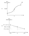
- the value of the drive voltage information Iv and the color correction value Gain (for example, the color correction value R_Gain for red and the color correction value B_Gain for blue).
- the value of the drive voltage information Iv and the color correction value Gain are associated with each other by the predetermined characteristic line for each value of the temperature information Item (low temperature, normal temperature, high temperature, etc.).
- the relationship between the drive voltage V and the light transmittance T in the light control element 22 (liquid crystal light control element) is generally defined by, for example, a characteristic curve composed of a cubic equation.
- the characteristic line defining the correspondence in the correction table 432 is also a characteristic curve composed of a cubic equation.
- the correction formula that defines the association in the correction table 432 is a cubic formula here.
- the color correction processing unit 43 uses the color correction value Gain obtained from the correction table 432 as described above, so that the color balance value in the imaging signal Sout is adjusted with the light amount of the imaging light Lout emitted from the dimming element 22.
- Color correction processing is performed so as to be substantially constant (preferably constant) without depending on both the temperature in the vicinity of the optical element 22.
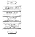
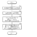
- the color correction processing unit 43 performs color correction processing as shown in FIG. 7, for example.
- the color correction processing unit 43 acquires the drive voltage information Iv and the temperature information Item from the light amount control unit 44 (steps S11 and S12 in FIG. 7). Next, the color correction processing unit 43 obtains the color correction value Gain from the correction table 432 described above using the drive voltage information Iv and the temperature information Item acquired in this manner (step S13).
- the cubic equation (approximate equation) in the correction table 432 at this time is, for example, the following equations (1) and (2). It should be noted that the coefficients a R , b R , c R , d R , a B , b B , c B , and d B in these equations are held in the correction table 432, respectively. In this way, first, the color correction value Gain by the drive voltage V is obtained.
- Rx a R ⁇ Vx 3 + b R ⁇ Vx 2 + c R ⁇ Vx + d R (1)
- Bx a B ⁇ Vx 3 + b B ⁇ Vx 2 + c B ⁇ Vx + d B (2)
- the color correction processing unit 43 obtains a color correction value Gain in consideration of the temperature indicated by the temperature information Item (the temperature in the vicinity of the light control element 22). This is because, as shown in FIG. 6B, the color correction value Gain differs depending on the temperature even if the drive voltage V is the same. However, as shown in FIG. 8B, for example, since there is a linear relationship between the temperature and the color correction value Gain, for example, a high temperature (here 70 ° C.) and a low temperature (here ⁇ 10 ° C.) The color correction values Gain are held in the correction table 432 only at two places.
- R (T X ) R (T ⁇ 10 ) + ⁇ ⁇ ⁇ R (T 70 ) ⁇ R (T ⁇ 10 ) ⁇ (3)
- B (T X ) B (T ⁇ 10 ) + ⁇ ⁇ ⁇ B (T 70 ) ⁇ B (T ⁇ 10 ) ⁇ (4)
- ⁇ [Tx / ⁇ 70 ⁇ ( ⁇ 10) ⁇ ] (5)
- color correction processing realizes color correction in consideration of information (light transmittance information Itra) regarding the amount of imaging light Lout emitted from the light control element 22.
- color correction is performed in consideration of temperature information (temperature information Item) in the vicinity of the light control element 22 in addition to information on the light amount (light transmittance information Itra).
- the dimming element 22 is used. Since the color correction processing is performed on the imaging signal S1 obtained through the above method, it is possible to realize color correction in consideration of such information regarding the amount of light. Therefore, it is possible to perform appropriate color correction on the imaging signal acquired using the light control element 22.
- color correction processing is performed using temperature information Item indicating the temperature in the vicinity of the light control element 22 in addition to the information on the light amount (light transmittance information Itra). Color reproduction including characteristics can be realized.
- FIG. 9 is a block diagram illustrating a schematic configuration of an imaging apparatus (imaging apparatus 1A) according to the second embodiment of the present disclosure.
- This imaging device 1A includes the signal processing unit 4A instead of the signal processing unit 4 in the imaging device 1 of the first embodiment, and other configurations are the same.
- the same components as those in the first embodiment are denoted by the same reference numerals, and description thereof will be omitted as appropriate.
- the signal processing unit 4A is provided with a color correction processing unit 43A instead of the color correction processing unit 43 in the signal processing unit 4 in the first embodiment, and other configurations are the same.
- the color correction processing unit 43A performs color correction processing using temperature information Item and light transmittance information Itra (light amount information) supplied from the light amount control unit 44. . That is, the color correction processing unit 43 performs color correction processing indirectly using information (light transmittance information Itra) regarding the light amount of the imaging light Lout, whereas the color correction processing unit 43A performs such a color correction processing. Color correction processing is performed by directly using information relating to the light amount of the imaging light Lout.
- the color correction processing unit 43A includes, for example, a color correction value calculation unit 431A, a correction table 432A, and a multiplication unit 433 as illustrated in FIG. That is, in the color correction processing unit 43, a color correction value calculation unit 431A and a correction table 432A (first correction table) are provided instead of the color correction value calculation unit 431 and the correction table 432, respectively.
- the color correction value calculation unit 431A uses the imaging signal S1, the light transmittance information Itra and the temperature information Item supplied from the light amount control unit 44, and the correction table 432A, and the color correction value Gain at the time of color correction processing. Is what you want.
- the correction table 432A is a table in which the light transmittance information Itra and the color correction value Gain are associated with each other in advance, and here, in particular, the temperature information Item is also associated with them. Such a correction table 432A is also held in advance on a storage unit (memory) (not shown), for example.
- a correction table 432A for example, as shown in FIG. 11A, the value of the light transmittance information Itra and the color correction value Gain (for example, the color correction value R_Gain for red, the color correction for blue). Value B_Gain) is associated with a predetermined characteristic line.
- the value of the light transmittance information Itra and the color correction value Gain correspond to each value of the temperature information Item (low temperature, normal temperature, high temperature, etc.) by a predetermined characteristic line. The ones attached are listed.
- the characteristic line that defines the correspondence in the correction table 432A is 1 because it is performed using the light transmittance information Itra directly as described above. It is a characteristic line consisting of the following formula.
- the correction formula that defines the association in the correction table 432A is a primary formula here. That is, the value of the light transmittance information Itra and the color correction value Gain have a linear relationship.
- the correction equation is a complex expression such as a cubic equation
- the correction equation is a linear equation. Therefore, a simpler and more accurate color correction process than that of the first embodiment is realized.
- a part of the color correction value Gain positioned on the correction equation can be interpolated and generated by linear interpolation (linear function interpolation). is there.
- linear interpolation linear function interpolation
- the interpolation may be generated by linear interpolation. In that case, the configuration of the correction table 432A becomes simpler (the data capacity is smaller).
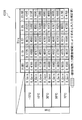
- FIG. 12 shows an example of such a correction table 432A more specifically.
- the value of the light transmittance information Itra (specified by the light transmittance ratio when the darkest state is used as a reference) and the color correction value Gain (red color correction value R_Gain, blue color correction value B_Gain) are associated with each value ( ⁇ 10 ° C. to 70 ° C.) of the temperature information Item.
- the same color correction processing as that of the first embodiment is performed using the color correction value Gain obtained from the correction table 432A. That is, the color balance value in the imaging signal Sout is substantially constant (preferably constant) without depending on both the light amount of the imaging light Lout emitted from the dimmer 22 and the temperature in the vicinity of the dimmer 22.
- color correction processing is performed. Specifically, in the present embodiment, the color correction processing unit 43A performs color correction processing as shown in FIG. 13, for example.
- the color correction processing unit 43A acquires the light transmittance information Itra and the temperature information Item from the light amount control unit 44 as described above (steps S21 and S22 in FIG. 13). Next, the color correction processing unit 43A obtains the color correction value Gain from the correction table 432A described above using the light transmittance information Itra and the temperature information Item acquired in this way (step S23).
- the color correction processing unit 43A holds only the coordinates of the two points P0 and P1 shown in FIG. 14, for example, in the correction table 432A.
- To (8) are used to determine the coordinates of the point Px that defines the color correction value Gain. In this way, first, the color correction value Gain based on the light transmittance is obtained.
- Rx R0 + a ⁇ (R1-R0) (6)
- Bx B0 + a ⁇ (B1-B0) (7)
- a (Ex / 1.33)
- the color correction processing unit 43A obtains a color correction value Gain in consideration of the temperature indicated by the temperature information Item (the temperature in the vicinity of the dimming element 22), similarly to step S13 described in the first embodiment. .
- the color correction processing is performed by directly using the information regarding the light amount of the imaging light Lout, so that the correction formula in the correction table 432A is a linear formula, and the first Compared with the present embodiment, a simple and accurate color correction process can be realized.
- FIG. 15A illustrates a block configuration of a color correction processing unit (color correction processing unit 43B) according to the first modification.
- FIG. 15B illustrates a block configuration of a color correction processing unit (color correction processing unit 43C) according to Modification 2.
- the color correction processing unit 43B according to Modification 1 is provided with a color correction value calculation unit 431B instead of the color correction value calculation unit 431 in the color correction processing unit 43 according to the first embodiment. Is the same.
- the color correction value calculation unit 431B does not use the temperature information Item supplied from the light amount control unit 44, but the drive voltage supplied from the light amount control unit 44. Color correction processing is performed using the information Iv. Therefore, in this modification, for example, the correction table 432 shown in FIG. 6A is used.
- the color correction processing unit 43C according to the modification 2 is obtained by providing a color correction value calculation unit 431C instead of the color correction value calculation unit 431A in the color correction processing unit 43A according to the second embodiment. Is the same.
- the color correction processing unit 43C differs from the color correction processing unit 43A in that the color correction value calculation unit 431C does not use the temperature information Item supplied from the light amount control unit 44 and transmits light transmitted from the light amount control unit 44. Color correction processing is performed using rate information Itra (light quantity information). Therefore, in this modification, for example, the correction table 432A shown in FIG. 11A is used.
- the color information is directly or indirectly used without using the temperature information Item supplied from the light quantity control unit 44 and using the information (light transmittance information Itra) regarding the light quantity of the imaging light Lout. Correction processing may be performed.
- the color balance value in the imaging signal Sout is substantially constant (preferably constant) without depending on the light amount of the imaging light Lout emitted from the light control element 22. Perform color correction processing.
- a liquid crystal light control element using a GH type liquid crystal has been described as an example.
- a dimming element other than a liquid crystal dimming element may be used.
- light control elements other than the liquid crystal light control elements include light control elements of the following method. That is, for example, thermochromism (practical examples: mugs, polymer sheets, etc.), dimmers using gel materials used for thermotropic, and photochromic (practical examples: sunglasses that change with ultraviolet rays, etc.) WO 3 (tungsten oxide), Nb 2 O 5 (niobium oxide) in a light control element using hydrogen gas or the like in an optical element, gas chromic (practical example: window glass, etc.), electrochromic (practical example: window glass, etc.) , NiO (nickel oxide), Cr 2 O 3 (chromium oxide), and the like.
- thermochromism (practical examples: mugs, polymer sheets, etc.), dimmers using gel materials used for thermotropic, and photochromic (practical examples: sunglasses that change with ultraviolet rays, etc.)
- WO 3 tungsten oxide
- Nb 2 O 5 niobium oxide
- gas chromic practical example: window
- each component (block configuration of the signal processing unit) of the imaging device has been specifically described, but it is not necessary to include all the components, and other components are not included. Furthermore, you may provide.
- the case where one lens (lens group) is provided in the imaging apparatus (on the optical path of the imaging light) has been described as an example, but the present invention is not limited thereto. That is, for example, a plurality of lenses (lens groups) may be provided on the optical path of the imaging light, or such lenses (lens groups) may not be provided in the imaging apparatus.
- the signal processing (color correction processing or the like) described in the above embodiments may be performed by hardware (circuit), or may be performed by software (program).
- the software includes a program group for causing each signal processing function (color correction processing function or the like) to be executed by a computer (such as a microcomputer in the imaging apparatus).
- Each program may be used by being incorporated in advance in dedicated hardware, for example, or installed in a general-purpose personal computer or the like from a network or a recording medium.
- this technique can also take the following structures.
- a light control element for adjusting the amount of incident imaging light;
- An image pickup device for acquiring an image pickup signal based on the image pickup light emitted from the light control device;
- a color correction processing unit that performs color correction on an imaging signal obtained by the imaging device based on information on the amount of imaging light emitted from the dimming device;
- the color correction processing unit performs the color correction so that a color balance value in the imaging signal becomes substantially constant without depending on the amount of imaging light emitted from the light control element.
- a light amount control unit that determines the light amount of the imaging light emitted from the light control element based on the signal value of the imaging signal, and outputs information on the light amount;
- a drive unit for determining a drive voltage for the light control element based on information on the light amount output from the light amount control unit, and supplying the drive voltage to the light control element;
- the imaging apparatus according to any one of (2) to (5), wherein the color correction processing unit acquires information on the light amount from the light amount control unit.
- the color correction processing unit performs the color correction by indirectly using information on the light amount.
- a light amount control unit that determines the light amount of the imaging light emitted from the light control element based on the signal value of the imaging signal, and outputs information on the light amount;
- a drive unit that determines the drive voltage based on information on the light amount output from the light amount control unit, and supplies the drive voltage to the dimming element; and
- the imaging apparatus according to (8) or (9), wherein the color correction processing unit acquires the driving voltage information from the driving unit via the light amount control unit.
- (11) The imaging according to any one of (1) to (10), wherein the color correction processing unit performs the color correction by using temperature information indicating a temperature in the vicinity of the light control element in addition to the information on the light amount. apparatus.
- the color correction processing unit is configured so that a color balance value in the imaging signal is substantially constant without depending on both the amount of imaging light emitted from the light control element and the temperature in the vicinity of the light control element.
- the information regarding the light amount is information indicating light transmittance in the light control element.
Landscapes
- Engineering & Computer Science (AREA)
- Multimedia (AREA)
- Signal Processing (AREA)
- Physics & Mathematics (AREA)
- General Physics & Mathematics (AREA)
- Color Television Image Signal Generators (AREA)
- Studio Devices (AREA)
- Liquid Crystal (AREA)
Abstract
Description
1.第1の実施の形態(駆動電圧情報および温度情報を用いて色補正を行う例)
2.第2の実施の形態(光透過率情報および温度情報を用いて色補正を行う例)
3・変形例
変形例1(駆動電圧情報を用いて色補正を行う例(温度情報を用いない例))
変形例2(光透過率情報を用いて色補正を行う例(温度情報を用いない例))
4.その他の変形例
Hereinafter, embodiments of the present disclosure will be described in detail with reference to the drawings. The description will be given in the following order.
1. First embodiment (example in which color correction is performed using drive voltage information and temperature information)
2. Second Embodiment (Example of performing color correction using light transmittance information and temperature information)
3. Modification Modification 1 (example in which color correction is performed using drive voltage information (example in which temperature information is not used))
Modification 2 (Example in which color correction is performed using light transmittance information (example in which temperature information is not used))
4). Other variations
[撮像装置1の構成]
図1は、本開示の第1の実施の形態に係る撮像装置(撮像装置1)の概略構成をブロック図で表したものである。この撮像装置1は、被写体からの光学的な画像を撮像素子(後述する撮像素子23)によって電気的な信号に変換する、デジタルカメラ(デジタルスチルカメラ)などである。なお、このようにして得られた撮像信号(デジタル信号)は、半導体記録媒体(図示せず)に記録したり、液晶ディスプレイ等の表示装置(図示せず)に表示したりすることが可能となっている。 <First Embodiment>
[Configuration of Imaging Device 1]
FIG. 1 is a block diagram illustrating a schematic configuration of an imaging apparatus (imaging apparatus 1) according to the first embodiment of the present disclosure. The
信号処理部4は、撮像素子23において得られた撮像信号Sinに対して所定の信号処理を行うとともに、調光素子22に対して所定のフィードバック制御(後述する光量制御)を行うものである。この信号処理部4は、S/H・AGC回路41、A/D変換部42、色補正処理部43および光量制御部(光透過率制御部)44を有している。 (Signal processing unit 4)
The
図2は、調光素子22(液晶調光素子)の断面構成例を模式的に表したものである。この調光素子22は、撮像光Linの入射側から撮像光Loutの出射側へと向かって、透明基板221a、透明電極222a、配向膜223a、液晶層220、配向膜223b、透明電極222bおよび透明基板221bがこの順に積層された積層構造を有している。調光素子22にはまた、シール剤224、スペーサ225および封止部226が設けられている。 [Detailed Configuration Example of Light Control Element 22]
FIG. 2 schematically illustrates a cross-sectional configuration example of the light control element 22 (liquid crystal light control element). The dimming
図3は、色補正処理部43の詳細構成例をブロック図で表わしたものである。この色補正処理部43は、色補正値演算部431、補正テーブル432(第2の補正テーブル)および乗算部433を有している。 [Detailed Configuration Example of Color Correction Processing Unit 43]
FIG. 3 is a block diagram illustrating a detailed configuration example of the color
(1.撮像動作)
この撮像装置1では、図1に示したように、レンズ21から出射された撮像光Linが調光素子22へ入射し、その光量(透過光量)が調整されて撮像光Loutとして出射する。この撮像光Loutは、撮像素子23へ入射して検出され、撮像信号Sinが得られる。 [Operation and Effect of Imaging Device 1]
(1. Imaging operation)
In the
ところで、このような調光素子を介して得られた撮像信号では一般に、状況に応じて撮像信号における色バランス(色合い,ホワイトバランス)がずれてしまい、撮像画質が低下してしまう場合がある。 (2. Color correction processing)
By the way, in general, in an imaging signal obtained through such a dimming element, the color balance (hue, white balance) in the imaging signal may be shifted depending on the situation, and the imaging quality may be degraded.
Rx=aR×Vx3+bR×Vx2+cR×Vx+dR ……(1)
Bx=aB×Vx3+bB×Vx2+cB×Vx+dB ……(2) Specifically, first, as shown in FIG. 8A, for example, from the drive voltage Vx indicated by the drive voltage information Iv, a color correction value Gain (for example, red color correction value R_Gain = Rx, for blue) Color correction value B_Gain = Bx) is obtained. The cubic equation (approximate equation) in the correction table 432 at this time is, for example, the following equations (1) and (2). It should be noted that the coefficients a R , b R , c R , d R , a B , b B , c B , and d B in these equations are held in the correction table 432, respectively. In this way, first, the color correction value Gain by the drive voltage V is obtained.
Rx = a R × Vx 3 + b R × Vx 2 + c R × Vx + d R (1)
Bx = a B × Vx 3 + b B × Vx 2 + c B × Vx + d B (2)
R(TX)=R(T-10)+α×{R(T70)-R(T-10)} ……(3)
B(TX)=B(T-10)+α×{B(T70)-B(T-10)} ……(4)
α=[Tx/{70-(-10)}] ……(5) Next, for example, as illustrated in FIG. 8B, the color
R (T X ) = R (T −10 ) + α × {R (T 70 ) −R (T −10 )} (3)
B (T X ) = B (T −10 ) + α × {B (T 70 ) −B (T −10 )} (4)
α = [Tx / {70 − (− 10)}] (5)
[撮像装置1Aの構成]
図9は、本開示の第2の実施の形態に係る撮像装置(撮像装置1A)の概略構成をブロック図で表したものである。この撮像装置1Aは、第1の実施の形態の撮像装置1において、信号処理部4の代わりに信号処理部4Aを備えたものであり、他の構成は同様となっている。なお、以下では、第1の実施の形態における構成要素と同一のものには同一の符号を付し、適宜説明を省略する。 <Second Embodiment>
[Configuration of
FIG. 9 is a block diagram illustrating a schematic configuration of an imaging apparatus (
Rx=R0+a×(R1-R0) ……(6)
Bx=B0+a×(B1-B0) ……(7)
a=(Ex/1.33) ……(8) Specifically, first, as shown in FIG. 14, for example, the color correction value Gain (for example, R_Gain = Rx, B_Gain = Bx) is obtained from the light transmittance Ex indicated by the light transmittance information Itra. At this time, unlike the first embodiment, the color
Rx = R0 + a × (R1-R0) (6)
Bx = B0 + a × (B1-B0) (7)
a = (Ex / 1.33) (8)
本実施の形態の撮像装置1Aにおいても、基本的には第1の実施の形態の撮像装置1と同様の作用により同様の効果を得ることが可能である。すなわち、光量に関する情報を考慮した色補正を実現することができ、調光素子22を用いて取得した撮像信号に対して適切な色補正を行うことが可能となる。また、光量に関する情報(光透過率情報Itra)に加えて、調光素子22近傍の温度を示す温度情報Itemをも用いて色補正処理を行っているため、温度特性も含めた色再現を実現することが可能となる。 [Operation and Effect of
Also in the
続いて、上記第1,第2の実施の形態の変形例(変形例1,2)について説明する。なお、これらの実施の形態における構成要素と同一のものには同一の符号を付し、適宜説明を省略する。 <Modification>
Subsequently, modified examples (modified examples 1 and 2) of the first and second embodiments will be described. In addition, the same code | symbol is attached | subjected to the same thing as the component in these embodiment, and description is abbreviate | omitted suitably.
図15(A)は、変形例1に係る色補正処理部(色補正処理部43B)のブロック構成を表したものである。また、図15(B)は、変形例2に係る色補正処理部(色補正処理部43C)のブロック構成を表したものである。 [
FIG. 15A illustrates a block configuration of a color correction processing unit (color
以上、いくつかの実施の形態および変形例を挙げて本開示の技術を説明したが、本技術はこれらの実施の形態等に限定されず、種々の変形が可能である。 <Other variations>
The technology of the present disclosure has been described above with some embodiments and modifications. However, the technology is not limited to these embodiments and the like, and various modifications can be made.
(1)
入射する撮像光の光量を調整する調光素子と、
前記調光素子から出射された撮像光に基づいて撮像信号を取得する撮像素子と、
前記調光素子から出射される撮像光の光量に関する情報に基づいて、前記撮像素子により得られた撮像信号に対する色補正を行う色補正処理部と
を備え、
前記色補正処理部は、前記撮像信号における色バランス値が、前記調光素子から出射される撮像光の光量に依存せずに略一定となるように、前記色補正を行う
撮像装置。
(2)
前記色補正処理部は、前記光量に関する情報を直接用いて前記色補正を行う
上記(1)に記載の撮像装置。
(3)
前記色補正処理部は、前記光量に関する情報と色補正値とを予め対応付けてなる第1の補正テーブルを用いて、前記色補正を行う
上記(2)に記載の撮像装置。
(4)
前記第1の補正テーブルにおける対応付けを規定する補正式が、1次式である
上記(3)に記載の撮像装置。
(5)
前記1次式上に位置する前記色補正値の一部が、線形補間により補間生成されたものである
上記(4)に記載の撮像装置。
(6)
前記撮像信号の信号値に基づいて前記調光素子から出射される撮像光の光量を決定し、前記光量に関する情報を出力する光量制御部と、
前記光量制御部から出力される光量に関する情報に基づいて前記調光素子に対する駆動電圧を決定し、その駆動電圧を前記調光素子へ供給する駆動部と
を備え、
前記色補正処理部は、前記光量に関する情報を前記光量制御部から取得する
上記(2)ないし(5)のいずれかに記載の撮像装置。
(7)
前記色補正処理部は、前記光量に関する情報を間接的に用いて前記色補正を行う
上記(1)に記載の撮像装置。
(8)
前記色補正処理部は、前記光量に関する情報に基づいて決定される、前記調光素子の駆動電圧を示す駆動電圧情報を用いて、前記色補正を行う
上記(7)に記載の撮像装置。
(9)
前記色補正処理部は、前記駆動電圧情報と色補正値とを予め対応付けてなる第2の補正テーブルを用いて、前記色補正を行う
上記(8)に記載の撮像装置。
(10)
前記撮像信号の信号値に基づいて前記調光素子から出射される撮像光の光量を決定し、前記光量に関する情報を出力する光量制御部と、
前記光量制御部から出力される光量に関する情報に基づいて前記駆動電圧を決定し、その駆動電圧を前記調光素子へ供給する駆動部と
を備え、
前記色補正処理部は、前記駆動部から前記光量制御部を介して前記駆動電圧情報を取得する
上記(8)または(9)に記載の撮像装置。
(11)
前記色補正処理部は、前記光量に関する情報に加えて、前記調光素子近傍の温度を示す温度情報を用いて、前記色補正を行う
上記(1)ないし(10)のいずれかに記載の撮像装置。
(12)
前記色補正処理部は、前記撮像信号における色バランス値が、前記調光素子から出射される撮像光の光量と前記調光素子近傍の温度との双方に依存せずに略一定となるように、前記色補正を行う
上記(11)に記載の撮像装置。
(13)
前記光量に関する情報が、前記調光素子における光透過率を示す情報である
上記(1)ないし(12)のいずれかに記載の撮像装置。
(14)
前記調光素子が液晶調光素子である
上記(1)ないし(13)のいずれかに記載の撮像装置。
(15)
前記撮像光の光路上に、1または複数のレンズを備えた
上記(1)ないし(14)のいずれかに記載の撮像装置。
(16)
入射する撮像光の光量を調整する調光素子から出射された撮像光に基づいて、撮像素子において撮像信号を取得するステップと、
前記調光素子から出射される撮像光の光量に関する情報に基づいて、前記撮像素子により得られた撮像信号に対する色補正を行うステップと
を含み、
前記色補正を行うステップでは、前記撮像信号における色バランス値が、前記調光素子から出射される撮像光の光量に依存せずに略一定となるように、前記色補正を行う
色補正方法。
(17)
入射する撮像光の光量を調整する調光素子から出射された撮像光に基づいて撮像素子により得られた撮像信号を取得するステップと、
前記調光素子から出射される撮像光の光量に関する情報に基づいて、前記撮像信号に対する色補正を行うステップと
をコンピュータに実行させると共に、
前記色補正を行うステップでは、前記撮像信号における色バランス値が、前記調光素子から出射される撮像光の光量に依存せずに略一定となるように、前記色補正を行う
色補正プログラム。 In addition, this technique can also take the following structures.
(1)
A light control element for adjusting the amount of incident imaging light;
An image pickup device for acquiring an image pickup signal based on the image pickup light emitted from the light control device;
A color correction processing unit that performs color correction on an imaging signal obtained by the imaging device based on information on the amount of imaging light emitted from the dimming device;
The color correction processing unit performs the color correction so that a color balance value in the imaging signal becomes substantially constant without depending on the amount of imaging light emitted from the light control element.
(2)
The imaging apparatus according to (1), wherein the color correction processing unit performs the color correction by directly using information regarding the light amount.
(3)
The imaging apparatus according to (2), wherein the color correction processing unit performs the color correction using a first correction table in which the information regarding the light amount and a color correction value are associated in advance.
(4)
The imaging apparatus according to (3), wherein the correction expression that defines the association in the first correction table is a linear expression.
(5)
The imaging apparatus according to (4), wherein a part of the color correction value positioned on the linear expression is generated by interpolation by linear interpolation.
(6)
A light amount control unit that determines the light amount of the imaging light emitted from the light control element based on the signal value of the imaging signal, and outputs information on the light amount;
A drive unit for determining a drive voltage for the light control element based on information on the light amount output from the light amount control unit, and supplying the drive voltage to the light control element;
The imaging apparatus according to any one of (2) to (5), wherein the color correction processing unit acquires information on the light amount from the light amount control unit.
(7)
The imaging apparatus according to (1), wherein the color correction processing unit performs the color correction by indirectly using information on the light amount.
(8)
The imaging apparatus according to (7), wherein the color correction processing unit performs the color correction by using drive voltage information indicating a drive voltage of the light control element, which is determined based on information on the light amount.
(9)
The imaging apparatus according to (8), wherein the color correction processing unit performs the color correction using a second correction table in which the driving voltage information and a color correction value are associated in advance.
(10)
A light amount control unit that determines the light amount of the imaging light emitted from the light control element based on the signal value of the imaging signal, and outputs information on the light amount;
A drive unit that determines the drive voltage based on information on the light amount output from the light amount control unit, and supplies the drive voltage to the dimming element; and
The imaging apparatus according to (8) or (9), wherein the color correction processing unit acquires the driving voltage information from the driving unit via the light amount control unit.
(11)
The imaging according to any one of (1) to (10), wherein the color correction processing unit performs the color correction by using temperature information indicating a temperature in the vicinity of the light control element in addition to the information on the light amount. apparatus.
(12)
The color correction processing unit is configured so that a color balance value in the imaging signal is substantially constant without depending on both the amount of imaging light emitted from the light control element and the temperature in the vicinity of the light control element. The imaging apparatus according to (11), wherein the color correction is performed.
(13)
The imaging apparatus according to any one of (1) to (12), wherein the information regarding the light amount is information indicating light transmittance in the light control element.
(14)
The imaging device according to any one of (1) to (13), wherein the light control element is a liquid crystal light control element.
(15)
The imaging apparatus according to any one of (1) to (14), wherein one or more lenses are provided on an optical path of the imaging light.
(16)
Acquiring an imaging signal in the imaging device based on imaging light emitted from the light control device that adjusts the amount of incident imaging light; and
Performing color correction on an imaging signal obtained by the imaging device based on information on the amount of imaging light emitted from the light control device, and
The color correction method of performing the color correction in the step of performing the color correction, so that a color balance value in the imaging signal becomes substantially constant without depending on a light amount of the imaging light emitted from the light control element.
(17)
Acquiring an imaging signal obtained by the imaging device based on imaging light emitted from a light control device that adjusts the amount of incident imaging light; and
And performing a color correction on the imaging signal based on information on the amount of imaging light emitted from the light control element, and
A color correction program for performing the color correction so that the color balance value in the imaging signal is substantially constant without depending on the amount of imaging light emitted from the light control element.
Claims (17)
- 入射する撮像光の光量を調整する調光素子と、
前記調光素子から出射された撮像光に基づいて撮像信号を取得する撮像素子と、
前記調光素子から出射される撮像光の光量に関する情報に基づいて、前記撮像素子により得られた撮像信号に対する色補正を行う色補正処理部と
を備え、
前記色補正処理部は、前記撮像信号における色バランス値が、前記調光素子から出射される撮像光の光量に依存せずに略一定となるように、前記色補正を行う
撮像装置。 A light control element for adjusting the amount of incident imaging light;
An image pickup device for acquiring an image pickup signal based on the image pickup light emitted from the light control device;
A color correction processing unit that performs color correction on an imaging signal obtained by the imaging device based on information on the amount of imaging light emitted from the dimming device;
The color correction processing unit performs the color correction so that a color balance value in the imaging signal becomes substantially constant without depending on the amount of imaging light emitted from the light control element. - 前記色補正処理部は、前記光量に関する情報を直接用いて前記色補正を行う
請求項1に記載の撮像装置。 The imaging apparatus according to claim 1, wherein the color correction processing unit performs the color correction by directly using information on the light amount. - 前記色補正処理部は、前記光量に関する情報と色補正値とを予め対応付けてなる第1の補正テーブルを用いて、前記色補正を行う
請求項2に記載の撮像装置。 The imaging apparatus according to claim 2, wherein the color correction processing unit performs the color correction using a first correction table in which information on the light amount and a color correction value are associated in advance. - 前記第1の補正テーブルにおける対応付けを規定する補正式が、1次式である
請求項3に記載の撮像装置。 The imaging apparatus according to claim 3, wherein the correction expression that defines the association in the first correction table is a linear expression. - 前記1次式上に位置する前記色補正値の一部が、線形補間により補間生成されたものである
請求項4に記載の撮像装置。 The imaging apparatus according to claim 4, wherein a part of the color correction value located on the linear expression is generated by interpolation by linear interpolation. - 前記撮像信号の信号値に基づいて前記調光素子から出射される撮像光の光量を決定し、前記光量に関する情報を出力する光量制御部と、
前記光量制御部から出力される光量に関する情報に基づいて前記調光素子に対する駆動電圧を決定し、その駆動電圧を前記調光素子へ供給する駆動部と
を備え、
前記色補正処理部は、前記光量に関する情報を前記光量制御部から取得する
請求項2に記載の撮像装置。 A light amount control unit that determines the light amount of the imaging light emitted from the light control element based on the signal value of the imaging signal, and outputs information on the light amount;
A drive unit for determining a drive voltage for the light control element based on information on the light amount output from the light amount control unit, and supplying the drive voltage to the light control element;
The imaging apparatus according to claim 2, wherein the color correction processing unit acquires information on the light amount from the light amount control unit. - 前記色補正処理部は、前記光量に関する情報を間接的に用いて前記色補正を行う
請求項1に記載の撮像装置。 The imaging apparatus according to claim 1, wherein the color correction processing unit performs the color correction by indirectly using information on the light amount. - 前記色補正処理部は、前記光量に関する情報に基づいて決定される、前記調光素子の駆動電圧を示す駆動電圧情報を用いて、前記色補正を行う
請求項7に記載の撮像装置。 The imaging apparatus according to claim 7, wherein the color correction processing unit performs the color correction by using drive voltage information indicating a drive voltage of the dimming element, which is determined based on information on the light amount. - 前記色補正処理部は、前記駆動電圧情報と色補正値とを予め対応付けてなる第2の補正テーブルを用いて、前記色補正を行う
請求項8に記載の撮像装置。 The imaging apparatus according to claim 8, wherein the color correction processing unit performs the color correction using a second correction table in which the drive voltage information and a color correction value are associated in advance. - 前記撮像信号の信号値に基づいて前記調光素子から出射される撮像光の光量を決定し、前記光量に関する情報を出力する光量制御部と、
前記光量制御部から出力される光量に関する情報に基づいて前記駆動電圧を決定し、その駆動電圧を前記調光素子へ供給する駆動部と
を備え、
前記色補正処理部は、前記駆動部から前記光量制御部を介して前記駆動電圧情報を取得する
請求項8に記載の撮像装置。 A light amount control unit that determines the light amount of the imaging light emitted from the light control element based on the signal value of the imaging signal, and outputs information on the light amount;
A drive unit that determines the drive voltage based on information on the light amount output from the light amount control unit, and supplies the drive voltage to the dimming element; and
The imaging apparatus according to claim 8, wherein the color correction processing unit acquires the drive voltage information from the drive unit via the light amount control unit. - 前記色補正処理部は、前記光量に関する情報に加えて、前記調光素子近傍の温度を示す温度情報を用いて、前記色補正を行う
請求項1に記載の撮像装置。 The imaging apparatus according to claim 1, wherein the color correction processing unit performs the color correction using temperature information indicating a temperature in the vicinity of the dimming element in addition to the information on the light amount. - 前記色補正処理部は、前記撮像信号における色バランス値が、前記調光素子から出射される撮像光の光量と前記調光素子近傍の温度との双方に依存せずに略一定となるように、前記色補正を行う
請求項11に記載の撮像装置。 The color correction processing unit is configured so that a color balance value in the imaging signal is substantially constant without depending on both the amount of imaging light emitted from the light control element and the temperature in the vicinity of the light control element. The imaging apparatus according to claim 11, wherein the color correction is performed. - 前記光量に関する情報が、前記調光素子における光透過率を示す情報である
請求項1に記載の撮像装置。 The imaging device according to claim 1, wherein the information regarding the amount of light is information indicating light transmittance in the light control element. - 前記調光素子が液晶調光素子である
請求項1に記載の撮像装置。 The imaging device according to claim 1, wherein the light control element is a liquid crystal light control element. - 前記撮像光の光路上に、1または複数のレンズを備えた
請求項1に記載の撮像装置。 The imaging device according to claim 1, further comprising one or more lenses on an optical path of the imaging light. - 入射する撮像光の光量を調整する調光素子から出射された撮像光に基づいて、撮像素子において撮像信号を取得することと、
前記調光素子から出射される撮像光の光量に関する情報に基づいて、前記撮像素子により得られた撮像信号に対する色補正を行うことと
を含み、
前記色補正を行うことにおいて、前記撮像信号における色バランス値が、前記調光素子から出射される撮像光の光量に依存せずに略一定となるように、前記色補正を行う
色補正方法。 Acquiring an imaging signal in the imaging element based on the imaging light emitted from the light control element that adjusts the amount of incident imaging light; and
Performing color correction on the imaging signal obtained by the imaging device based on information on the amount of imaging light emitted from the light control device, and
A color correction method for performing color correction such that, in performing the color correction, a color balance value in the imaging signal is substantially constant without depending on the amount of imaging light emitted from the light control element. - 入射する撮像光の光量を調整する調光素子から出射された撮像光に基づいて撮像素子により得られた撮像信号を取得することと、
前記調光素子から出射される撮像光の光量に関する情報に基づいて、前記撮像信号に対する色補正を行うことと
をコンピュータに実行させると共に、
前記色補正を行うことにおいて、前記撮像信号における色バランス値が、前記調光素子から出射される撮像光の光量に依存せずに略一定となるように、前記色補正を行う
色補正プログラム。 Acquiring an imaging signal obtained by the imaging element based on imaging light emitted from a light control element that adjusts the amount of incident imaging light; and
Causing the computer to perform color correction on the imaging signal based on information on the amount of imaging light emitted from the light control element, and
A color correction program for performing color correction so that, in performing the color correction, a color balance value in the imaging signal is substantially constant without depending on the amount of imaging light emitted from the light control element.
Priority Applications (6)
| Application Number | Priority Date | Filing Date | Title |
|---|---|---|---|
| US14/354,734 US9398281B2 (en) | 2011-12-02 | 2012-11-13 | Image pickup apparatus, color correction method, and color correction program |
| RU2014121227/07A RU2014121227A (en) | 2011-12-02 | 2012-11-13 | PICTURE IMAGE DEVICE, COLOR CORRECTION METHOD AND COLOR CORRECTION PROGRAM |
| EP12852756.1A EP2787730A4 (en) | 2011-12-02 | 2012-11-13 | Imaging device, colour-correction method and colour-correction program |
| IN980MUN2014 IN2014MN00980A (en) | 2011-12-02 | 2012-11-13 | |
| CN201280057946.0A CN103975584B (en) | 2011-12-02 | 2012-11-13 | Image pick up equipment and color calibration method |
| BR112014012685A BR112014012685A8 (en) | 2011-12-02 | 2012-11-13 | Imaging apparatus and color correction method and program |
Applications Claiming Priority (2)
| Application Number | Priority Date | Filing Date | Title |
|---|---|---|---|
| JP2011264959A JP5834850B2 (en) | 2011-12-02 | 2011-12-02 | Imaging apparatus, color correction method, and color correction program |
| JP2011-264959 | 2011-12-02 |
Publications (1)
| Publication Number | Publication Date |
|---|---|
| WO2013080785A1 true WO2013080785A1 (en) | 2013-06-06 |
Family
ID=48535252
Family Applications (1)
| Application Number | Title | Priority Date | Filing Date |
|---|---|---|---|
| PCT/JP2012/079390 WO2013080785A1 (en) | 2011-12-02 | 2012-11-13 | Imaging device, colour-correction method and colour-correction program |
Country Status (8)
| Country | Link |
|---|---|
| US (1) | US9398281B2 (en) |
| EP (1) | EP2787730A4 (en) |
| JP (1) | JP5834850B2 (en) |
| CN (1) | CN103975584B (en) |
| BR (1) | BR112014012685A8 (en) |
| IN (1) | IN2014MN00980A (en) |
| RU (1) | RU2014121227A (en) |
| WO (1) | WO2013080785A1 (en) |
Families Citing this family (3)
| Publication number | Priority date | Publication date | Assignee | Title |
|---|---|---|---|---|
| KR102481355B1 (en) * | 2015-09-30 | 2022-12-27 | 다이니폰 인사츠 가부시키가이샤 | dimming cell |
| WO2017203929A1 (en) * | 2016-05-25 | 2017-11-30 | シャープ株式会社 | Dimming device |
| JP6936650B2 (en) * | 2017-07-27 | 2021-09-22 | 三菱パワー株式会社 | Model learning device, trained model generation method, program, trained model, monitoring device, and monitoring method |
Citations (5)
| Publication number | Priority date | Publication date | Assignee | Title |
|---|---|---|---|---|
| JPH0654253A (en) * | 1992-07-30 | 1994-02-25 | Canon Inc | Camera |
| JPH0678208A (en) * | 1992-08-24 | 1994-03-18 | Canon Inc | Video camera |
| JPH1032832A (en) * | 1996-07-17 | 1998-02-03 | Canon Inc | Video camera |
| JP2001142050A (en) | 1999-11-12 | 2001-05-25 | Sony Corp | Light control device, image pickup device and their driving method |
| JP2011017819A (en) * | 2009-07-08 | 2011-01-27 | Sony Corp | Imaging optical system and imaging apparatus |
Family Cites Families (4)
| Publication number | Priority date | Publication date | Assignee | Title |
|---|---|---|---|---|
| US6952233B2 (en) * | 1992-07-23 | 2005-10-04 | Canon Kabushiki Kaisha | Video camera having a material element for controlling light transmission |
| JP3922238B2 (en) * | 2003-10-22 | 2007-05-30 | ソニー株式会社 | Light amount control device and camera device |
| JP4333478B2 (en) * | 2004-05-27 | 2009-09-16 | 株式会社ニコン | Imaging apparatus and image processing program |
| JP4438696B2 (en) * | 2005-06-15 | 2010-03-24 | セイコーエプソン株式会社 | Image display apparatus and method |
-
2011
- 2011-12-02 JP JP2011264959A patent/JP5834850B2/en active Active
-
2012
- 2012-11-13 BR BR112014012685A patent/BR112014012685A8/en not_active Application Discontinuation
- 2012-11-13 RU RU2014121227/07A patent/RU2014121227A/en not_active Application Discontinuation
- 2012-11-13 EP EP12852756.1A patent/EP2787730A4/en not_active Withdrawn
- 2012-11-13 WO PCT/JP2012/079390 patent/WO2013080785A1/en active Application Filing
- 2012-11-13 IN IN980MUN2014 patent/IN2014MN00980A/en unknown
- 2012-11-13 US US14/354,734 patent/US9398281B2/en active Active
- 2012-11-13 CN CN201280057946.0A patent/CN103975584B/en active Active
Patent Citations (5)
| Publication number | Priority date | Publication date | Assignee | Title |
|---|---|---|---|---|
| JPH0654253A (en) * | 1992-07-30 | 1994-02-25 | Canon Inc | Camera |
| JPH0678208A (en) * | 1992-08-24 | 1994-03-18 | Canon Inc | Video camera |
| JPH1032832A (en) * | 1996-07-17 | 1998-02-03 | Canon Inc | Video camera |
| JP2001142050A (en) | 1999-11-12 | 2001-05-25 | Sony Corp | Light control device, image pickup device and their driving method |
| JP2011017819A (en) * | 2009-07-08 | 2011-01-27 | Sony Corp | Imaging optical system and imaging apparatus |
Non-Patent Citations (1)
| Title |
|---|
| See also references of EP2787730A4 |
Also Published As
| Publication number | Publication date |
|---|---|
| BR112014012685A2 (en) | 2017-06-13 |
| EP2787730A4 (en) | 2015-11-18 |
| CN103975584A (en) | 2014-08-06 |
| CN103975584B (en) | 2016-08-24 |
| IN2014MN00980A (en) | 2015-04-24 |
| EP2787730A1 (en) | 2014-10-08 |
| US20140300772A1 (en) | 2014-10-09 |
| BR112014012685A8 (en) | 2017-06-20 |
| US9398281B2 (en) | 2016-07-19 |
| JP5834850B2 (en) | 2015-12-24 |
| RU2014121227A (en) | 2015-12-10 |
| JP2013118503A (en) | 2013-06-13 |
Similar Documents
| Publication | Publication Date | Title |
|---|---|---|
| JP2013150167A (en) | Imaging apparatus, color correction method, and color correction program | |
| US8659722B2 (en) | Optical device and imaging device | |
| JP6198235B2 (en) | Imaging device | |
| JP3201801B2 (en) | Projection display device | |
| JP2013114030A (en) | Liquid crystal dimmer, image pickup unit, and method of driving liquid crystal dimming element | |
| US20060279502A1 (en) | Method for fabricating liquid crystal display panel | |
| JP6838203B2 (en) | How to detect grayscale correction data on the liquid crystal display panel | |
| US11665436B2 (en) | Imaging device and camera system | |
| WO2019085667A1 (en) | Display device and display driving method | |
| EP4170417A1 (en) | Display device and display optimization method | |
| JP5834850B2 (en) | Imaging apparatus, color correction method, and color correction program | |
| WO2012056978A1 (en) | Image pickup device | |
| WO2021253495A1 (en) | Display device and display optimization method | |
| JP2011209514A (en) | Image display device and image display method | |
| JP2007081544A (en) | Photographing apparatus | |
| JP2009224993A (en) | Differential interface device, display control device, and display | |
| JP6693528B2 (en) | Dimming drive device, imaging device, dimming drive method | |
| JP2007104419A (en) | Photographing apparatus | |
| TWI272420B (en) | Display device | |
| JP5002665B2 (en) | Liquid crystal display | |
| JP2007094083A (en) | Photographing apparatus | |
| JP2004004548A (en) | Method and apparatus for sparkle reduction by limiting reactive and anticipatory slew rate | |
| JP2021076821A (en) | Liquid crystal display device | |
| JP2004109572A (en) | Liquid crystal display device | |
| JP2006119205A (en) | Liquid crystal display device and its black voltage setting method |
Legal Events
| Date | Code | Title | Description |
|---|---|---|---|
| 121 | Ep: the epo has been informed by wipo that ep was designated in this application |
Ref document number: 12852756 Country of ref document: EP Kind code of ref document: A1 |
|
| WWE | Wipo information: entry into national phase |
Ref document number: 14354734 Country of ref document: US |
|
| ENP | Entry into the national phase |
Ref document number: 2014121227 Country of ref document: RU Kind code of ref document: A |
|
| NENP | Non-entry into the national phase |
Ref country code: DE |
|
| REG | Reference to national code |
Ref country code: BR Ref legal event code: B01A Ref document number: 112014012685 Country of ref document: BR |
|
| ENP | Entry into the national phase |
Ref document number: 112014012685 Country of ref document: BR Kind code of ref document: A2 Effective date: 20140526 |