WO2013076937A1 - Circuit de conversion de c.a. - Google Patents
Circuit de conversion de c.a. Download PDFInfo
- Publication number
- WO2013076937A1 WO2013076937A1 PCT/JP2012/007333 JP2012007333W WO2013076937A1 WO 2013076937 A1 WO2013076937 A1 WO 2013076937A1 JP 2012007333 W JP2012007333 W JP 2012007333W WO 2013076937 A1 WO2013076937 A1 WO 2013076937A1
- Authority
- WO
- WIPO (PCT)
- Prior art keywords
- voltage
- switching
- unit
- input
- phase
- Prior art date
Links
Images

Classifications
-
- H—ELECTRICITY
- H02—GENERATION; CONVERSION OR DISTRIBUTION OF ELECTRIC POWER
- H02M—APPARATUS FOR CONVERSION BETWEEN AC AND AC, BETWEEN AC AND DC, OR BETWEEN DC AND DC, AND FOR USE WITH MAINS OR SIMILAR POWER SUPPLY SYSTEMS; CONVERSION OF DC OR AC INPUT POWER INTO SURGE OUTPUT POWER; CONTROL OR REGULATION THEREOF
- H02M5/00—Conversion of ac power input into ac power output, e.g. for change of voltage, for change of frequency, for change of number of phases
- H02M5/40—Conversion of ac power input into ac power output, e.g. for change of voltage, for change of frequency, for change of number of phases with intermediate conversion into dc
- H02M5/42—Conversion of ac power input into ac power output, e.g. for change of voltage, for change of frequency, for change of number of phases with intermediate conversion into dc by static converters
- H02M5/44—Conversion of ac power input into ac power output, e.g. for change of voltage, for change of frequency, for change of number of phases with intermediate conversion into dc by static converters using discharge tubes or semiconductor devices to convert the intermediate dc into ac
- H02M5/453—Conversion of ac power input into ac power output, e.g. for change of voltage, for change of frequency, for change of number of phases with intermediate conversion into dc by static converters using discharge tubes or semiconductor devices to convert the intermediate dc into ac using devices of a triode or transistor type requiring continuous application of a control signal
- H02M5/458—Conversion of ac power input into ac power output, e.g. for change of voltage, for change of frequency, for change of number of phases with intermediate conversion into dc by static converters using discharge tubes or semiconductor devices to convert the intermediate dc into ac using devices of a triode or transistor type requiring continuous application of a control signal using semiconductor devices only
-
- H—ELECTRICITY
- H02—GENERATION; CONVERSION OR DISTRIBUTION OF ELECTRIC POWER
- H02M—APPARATUS FOR CONVERSION BETWEEN AC AND AC, BETWEEN AC AND DC, OR BETWEEN DC AND DC, AND FOR USE WITH MAINS OR SIMILAR POWER SUPPLY SYSTEMS; CONVERSION OF DC OR AC INPUT POWER INTO SURGE OUTPUT POWER; CONTROL OR REGULATION THEREOF
- H02M5/00—Conversion of ac power input into ac power output, e.g. for change of voltage, for change of frequency, for change of number of phases
- H02M5/02—Conversion of ac power input into ac power output, e.g. for change of voltage, for change of frequency, for change of number of phases without intermediate conversion into dc
- H02M5/04—Conversion of ac power input into ac power output, e.g. for change of voltage, for change of frequency, for change of number of phases without intermediate conversion into dc by static converters
- H02M5/22—Conversion of ac power input into ac power output, e.g. for change of voltage, for change of frequency, for change of number of phases without intermediate conversion into dc by static converters using discharge tubes with control electrode or semiconductor devices with control electrode
- H02M5/275—Conversion of ac power input into ac power output, e.g. for change of voltage, for change of frequency, for change of number of phases without intermediate conversion into dc by static converters using discharge tubes with control electrode or semiconductor devices with control electrode using devices of a triode or transistor type requiring continuous application of a control signal
- H02M5/297—Conversion of ac power input into ac power output, e.g. for change of voltage, for change of frequency, for change of number of phases without intermediate conversion into dc by static converters using discharge tubes with control electrode or semiconductor devices with control electrode using devices of a triode or transistor type requiring continuous application of a control signal for conversion of frequency
-
- H—ELECTRICITY
- H02—GENERATION; CONVERSION OR DISTRIBUTION OF ELECTRIC POWER
- H02M—APPARATUS FOR CONVERSION BETWEEN AC AND AC, BETWEEN AC AND DC, OR BETWEEN DC AND DC, AND FOR USE WITH MAINS OR SIMILAR POWER SUPPLY SYSTEMS; CONVERSION OF DC OR AC INPUT POWER INTO SURGE OUTPUT POWER; CONTROL OR REGULATION THEREOF
- H02M7/00—Conversion of ac power input into dc power output; Conversion of dc power input into ac power output
- H02M7/42—Conversion of dc power input into ac power output without possibility of reversal
- H02M7/44—Conversion of dc power input into ac power output without possibility of reversal by static converters
- H02M7/48—Conversion of dc power input into ac power output without possibility of reversal by static converters using discharge tubes with control electrode or semiconductor devices with control electrode
- H02M7/4826—Conversion of dc power input into ac power output without possibility of reversal by static converters using discharge tubes with control electrode or semiconductor devices with control electrode operating from a resonant DC source, i.e. the DC input voltage varies periodically, e.g. resonant DC-link inverters
Definitions
- the present application relates to a technique for converting a relatively high frequency AC voltage into a relatively low frequency AC voltage.
- Patent Document 1 discloses a new wireless energy transmission device that transmits energy through space using an electromagnetic coupling phenomenon between two resonators.
- vibration energy is wirelessly (contactlessly) connected by coupling two resonators through a vibration energy exudation (evanescent tail) generated in a space around the resonator.
- evanescent tail vibration energy exudation
- the output power of the resonator in this wireless power transmission system is AC power having a frequency equal to the resonance frequency, and the resonance frequency is usually set to 100 kHz or higher.
- this high-frequency AC power is used as general household power, it is necessary to convert it to 50/60 Hz low-frequency AC power used in the system power supply.
- Patent Document 2 discloses general inverter technology. In the conversion method, input AC power is temporarily converted into DC power, and then AC power is obtained by switching the direction of current with respect to a load using a plurality of switching elements. At this time, the output frequency is determined by the switching frequency of the switching element.
- the present disclosure provides an AC conversion circuit that can suppress a decrease in conversion efficiency when AC power having a relatively high frequency input from a wireless power transmission system or the like is converted into AC power having a relatively low frequency.
- an AC conversion circuit is an AC that converts a single-phase input AC voltage having a frequency f0 into a three-phase output AC voltage having a frequency f1 lower than the frequency f0.
- a switching circuit that converts the input AC voltage based on a control signal and outputs the converted voltage to a phase selected based on the control signal; and a high-frequency component of the converted voltage
- the filter unit that converts the converted voltage into the output AC voltage by removing the reference, and the frequency f1 corresponding to the output AC voltage of each phase in synchronization with the timing when the input AC voltage becomes 0 Pulse density modulation is performed for each phase based on the signal, the control signal is generated based on the generation status of the pulse by the pulse density modulation, and the polarity of the input AC voltage, and the control And a switching control unit for sending to the switching unit to issue.
- the switching unit corresponds to a first type of switching element that applies a positive voltage to a corresponding phase when the polarity of the input AC voltage is positive, and a positive voltage when the polarity of the input AC voltage is negative. And a second type of switching element applied to the phase.
- the switching control unit turns on the first type switching element when the polarity of the input AC voltage is positive and the polarity of the reference signal in the pulse density modulation is positive, When the polarity is negative and the polarity of the reference signal in the pulse density modulation is positive, the switching element of the second type is turned on, the polarity of the input AC voltage is positive, and the polarity in the pulse density modulation is When the polarity of the reference signal is negative, the second type switching element is turned on, the polarity of the input AC voltage is negative, and the polarity of the reference signal in the pulse density modulation is negative, The first type switching element is turned on, and the first type switching element and the second switching element correspond to the same phase. So as not to turn towards the same time, it outputs the control signal for controlling the switching unit.
- the switching control unit performs the pulse density modulation based on space vector modulation.
- An AC conversion circuit is an AC conversion circuit that converts a single-phase input AC voltage having a frequency f0 into a three-phase output AC voltage having a frequency f1 lower than the frequency f0.
- a converter unit that converts an input AC voltage into a DC voltage; a switching unit that converts the DC voltage based on a control signal; and outputs the converted voltage to a phase selected based on the control signal; and the conversion
- a filter unit that converts the converted voltage into the output AC voltage by removing a high-frequency component of the subsequent voltage, and an output AC voltage of each phase in synchronization with the timing when the input AC voltage becomes 0 Pulse density modulation is performed for each phase based on the reference signal of the corresponding frequency f1, and the control signal is generated based on the pulse generation status by the pulse density modulation, and the switching And a switching control unit to be sent to the.
- the switching unit corresponds to a first type of switching element that applies a positive voltage to a corresponding phase when the polarity of the input AC voltage is positive, and a positive voltage when the polarity of the input AC voltage is negative. And a second type of switching element applied to the phase.
- the switching control unit turns on the first type switching element, and when the polarity of the reference signal in the pulse density modulation is negative Switching the second type switching element so as not to simultaneously turn on both the first type switching element and the second switching element corresponding to the same phase.
- the control signal for controlling the unit is output.
- the switching control unit performs the pulse density modulation based on space vector modulation.
- the switching operation is performed when the input voltage of the input high-frequency AC power is zero, power conversion with higher efficiency than before can be performed.
- FIG. It is a figure which shows the example of the three-phase sine wave output from a reference sine wave generation part. It is a figure which shows the structure of the space vector modulation part in 1st Embodiment. It is a figure for demonstrating the principle of space vector modulation. It is a figure which shows the relationship between a three-phase coordinate system and a two-phase coordinate system. It is a figure which shows 8 switching vectors and 6 sectors. It is a figure which shows the example of the command vector Vs in the sector 1.
- FIG. It is a figure which shows the example of the determination method of the switching state by the comparison with the duration of a carrier signal and each switching vector.
- FIG. 3 is a diagram illustrating waveforms of voltages in the first embodiment.
- A is a figure which shows the waveform of an input alternating voltage
- (b) is a figure which shows the output waveform of a switching part
- (c) is a figure which shows the output waveform of a filter.
- It is a figure which shows the structure of the alternating current converter circuit by 2nd Embodiment.
- It is a figure which shows the structure of the switching control part in 2nd Embodiment.
- (A) is a figure which shows the waveform of an input AC voltage
- (b) is a figure which shows the output waveform of a converter part
- (c) is a figure which shows the output waveform of a switching part
- (d) is a filter. It is a figure which shows the output waveform.
- (A) is a figure which shows the waveform of an input AC voltage
- (b) is a figure which shows the output waveform of a converter part
- (c) is a figure which shows the output waveform of a switching part
- (d) is a filter. It is a figure which shows the output waveform. It is a figure which shows the input-output waveform in embodiment which always outputs electric power only to one phase.
- (A) is a figure which shows the waveform of an input alternating voltage
- (b) is a figure which shows the output waveform of a converter part
- (c) is a figure which shows the output waveform of a switching part
- (d) is each figure It is a figure which shows the output waveform of the filter of a phase.
- An AC conversion circuit is an AC conversion circuit that converts a single-phase input AC voltage having a frequency f0 into a three-phase output AC voltage having a frequency f1 lower than the frequency f0. Converting the input AC voltage based on the output, and outputting the converted voltage to a phase selected based on the control signal, and removing the high-frequency component of the converted voltage, A pulse unit for each phase based on a reference signal having a frequency f1 corresponding to the output AC voltage of each phase in synchronization with a timing at which the input AC voltage becomes 0, and a filter unit that converts the subsequent voltage into the output AC voltage Density modulation is performed, the control signal is generated based on the pulse generation status by the pulse density modulation and the polarity of the input AC voltage, and the control signal is sent to the switching unit And a switching control unit.
- the switching unit corresponds to a first type of switching element that applies a positive voltage to a corresponding phase when the polarity of the input AC voltage is positive, and a positive voltage when the polarity of the input AC voltage is negative. And a second type of switching element applied to the phase.
- the switching control unit turns on the first type switching element when the polarity of the input AC voltage is positive and the polarity of the reference signal in the pulse density modulation is positive, When the polarity is negative and the polarity of the reference signal in the pulse density modulation is positive, the switching element of the second type is turned on, the polarity of the input AC voltage is positive, and the polarity in the pulse density modulation is When the polarity of the reference signal is negative, the second type switching element is turned on, the polarity of the input AC voltage is negative, and the polarity of the reference signal in the pulse density modulation is negative, The first type switching element is turned on, and the first type switching element and the second switching element correspond to the same phase. So as not to turn towards the same time, it outputs the control signal for controlling the switching unit.
- the switching control unit performs the pulse density modulation based on space vector modulation.
- An AC conversion circuit is an AC conversion circuit that converts a single-phase input AC voltage having a frequency f0 into a three-phase output AC voltage having a frequency f1 lower than the frequency f0.
- a converter unit that converts an input AC voltage into a DC voltage; a switching unit that converts the DC voltage based on a control signal; and outputs the converted voltage to a phase selected based on the control signal; and the conversion
- a filter unit that converts the converted voltage into the output AC voltage by removing a high-frequency component of the subsequent voltage, and an output AC voltage of each phase in synchronization with the timing when the input AC voltage becomes 0 Pulse density modulation is performed for each phase based on the reference signal of the corresponding frequency f1, and the control signal is generated based on the pulse generation status by the pulse density modulation.
- the switching unit corresponds to a first type of switching element that applies a positive voltage to a corresponding phase when the polarity of the input AC voltage is positive, and a positive voltage when the polarity of the input AC voltage is negative. And a second type of switching element applied to the phase.
- the switching control unit turns on the first type switching element, and when the polarity of the reference signal in the pulse density modulation is negative Switching the second type switching element so as not to simultaneously turn on both the first type switching element and the second switching element corresponding to the same phase.
- the control signal for controlling the unit is output.
- the switching control unit performs the pulse density modulation based on space vector modulation.
- the AC conversion circuit includes a snubber circuit for reducing unnecessary oscillation during switching between the converter unit and the switching unit.
- the snubber circuit includes a diode, a capacitor, and a resistor.
- the switching control unit generates a reference signal generating unit that generates three types of reference signals having a frequency f1 corresponding to the output AC voltage of each phase in synchronization with a timing when the input AC voltage becomes zero.
- a carrier signal generating unit that generates a carrier signal having a frequency higher than the frequency of the reference signal, the three types of reference signals generated by the reference signal generating unit, and the carrier generated by the carrier signal generating unit
- a space vector modulation unit that performs space vector modulation based on the signal.
- the space vector modulation unit determines a conduction state of each switching element in the switching unit based on the three types of reference signals, and determines a duration of the conduction state of each switching element using the carrier signal. .
- the space vector modulation unit converts the three types of reference signals into pulses by space vector modulation, and the pulse corresponds to each phase at a timing when the value of the input AC voltage becomes zero. Output to.
- the switching control unit is configured to control the control based on a positive / negative determination unit that determines the polarity of the input AC voltage, the pulse output from the space vector modulation unit, and a determination result of the positive / negative determination unit.
- a switching signal output unit that generates a signal and sends the signal to the switching unit.
- the switching control unit switches an on state and an off state of each switching element at a time interval equal to or more than a preset minimum on time and minimum off time, and the minimum on time and the minimum off time are: It is set to n1 / 2f0 (n1 is an integer of 2 or more).
- the switching control unit switches an on state and an off state of each switching element at a time interval equal to or less than a preset maximum on time and maximum off time, and the maximum on time and the maximum off time are: n2 / 2f0 (n2 is an integer of 2 or more) is set.
- the switching control unit controls the switching unit such that a voltage corresponding to a half cycle of the input AC voltage is always output only to a specific phase.
- the AC conversion circuit further includes a zero-crossing timing detection unit that detects a timing when the value of the input AC voltage becomes 0 and notifies the switching control unit of the timing.
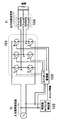
- FIG. 20 is a configuration diagram of a power receiving side AC conversion circuit that converts a high-frequency single-phase alternating current such as a wireless power transmission system into a lower-frequency three-phase alternating current using conventional inverter technology.
- This AC conversion circuit is arranged for each phase, a rectification unit 1401 that converts input high-frequency AC power into DC power, an inverter unit 1402 that outputs the output voltage of the rectification unit 1401 to each phase by a plurality of switching elements.
- a low-pass filter unit 104 hereinafter referred to as “filter”).
- the AC conversion circuit further includes a switching control unit 1403 that controls operations of a plurality of switching elements included in the inverter unit 1402.
- the operation of the AC conversion circuit shown in FIG. 20 will be described.
- the input high-frequency AC power is converted into DC power by the rectifier 1401.
- the switching elements U, V, W, X, Y, and Z are turned on and off so that the directions of the currents flowing through the loads of the respective phases are alternately switched.
- semiconductor switches such as MOSFETs and IGBTs are generally used.
- Pulse width modulation (PWM) is used for on / off timing control of each switching element.
- FIG. 21A and 21B are diagrams for explaining the configuration and operation of the switching control unit 1403.
- the switching control unit 1403 inputs a reference sine wave 1501 set to the same frequency as the frequency of the output low frequency power and a triangular wave 1502 preset to a frequency higher than the frequency.
- PWM controller 1503 for receiving the signal.
- the PWM control unit 1503 inputs a pulse generated based on the reference sine wave 1501 and the triangular wave 1502 to a gate of a predetermined switching element.
- FIG. 21B is a diagram illustrating an example of switching timing by the PWM control unit 1503.
- the PWM control unit 1503 compares the input values of the reference sine wave 1501 and the triangular wave 1502. When “reference sine wave ⁇ 0” and “reference sine wave ⁇ triangular wave”, switching element U and switching element Y are turned on, “reference sine wave ⁇ 0” and “reference sine wave ⁇ triangular wave”. In this case, the switching element U and the switching element Y are turned off.
- the DC power input to the inverter unit 1402 is converted into a pulse train having the same width as the pulse shown in FIG.
- the output pulse train passes through the low-pass filter unit 104 and is converted into a sine wave having a desired frequency as a final output.
- the configuration for obtaining a sine wave output has been described as an example. However, by making the reference sine wave an arbitrary frequency and waveform, the input high-frequency AC power is changed to an AC power having an arbitrary frequency and waveform. Can be converted to
- the present inventors have newly found the above-mentioned problem, and decrease in conversion efficiency when converting AC power of a relatively high frequency input from a wireless power transmission system or the like into AC power of a relatively low frequency.
- An AC conversion circuit that can suppress this problem has been completed.
- an outline of an embodiment in the present disclosure will be described.
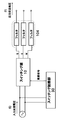
- FIG. 1A is a diagram illustrating a configuration example of an AC conversion circuit according to an embodiment of the present disclosure.
- the illustrated AC converter circuit converts a single-phase AC voltage having a frequency f0 (hereinafter, also referred to as “input AC voltage”) into a three-phase AC voltage having a frequency f1 lower than the frequency f0 (hereinafter, “ It may be referred to as “output AC voltage”).
- This AC conversion circuit converts an input AC voltage based on a control signal, outputs the converted voltage to each phase (between uv phase, vw phase, wu phase), and outputs a high frequency from the output of the switching unit 10
- a filter unit 104 that removes components and outputs an output AC voltage.
- the AC conversion circuit also includes a switching control unit 30 that controls the switching unit 10 by generating the control signal and inputting the control signal to the switching unit 10.
- the switching control unit 30 performs pulse density modulation for each phase based on the reference signal of the frequency f1 corresponding to the output AC voltage of each phase in synchronization with the timing when the input AC voltage becomes 0. Then, a control signal is generated based on the pulse generation status by pulse density modulation and the polarity of the input AC voltage, and is sent to the switching unit 10. The phase to which the converted voltage is output is selected by this control signal. The above operation is performed every time the input AC voltage becomes 0, that is, every half cycle of the input AC voltage.
- the “pulse generation status” means, for example, whether or not a pulse is generated for each phase, the polarity of the generated pulse, and the like.
- the switching unit 10 typically has a plurality of switching elements, and distributes the input voltage to three phases by switching on and off a specific switching element selected by the control signal.
- “ON” represents a conductive state
- “OFF” represents a non-conductive state.
- a desired three-phase alternating current can be dynamically generated according to the polarity of the input alternating voltage and the polarity of the output alternating voltage.
- the input AC voltage is 0 is not limited to being completely zero, but includes a range that can be regarded as substantially zero. In this specification, when the value with respect to the amplitude of the input AC voltage is included in the range of less than 10%, it is substantially zero.
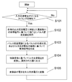
- FIG. 1B is a flowchart showing an operation flow of the AC conversion circuit shown in FIG. 1A.
- step S101 the timing at which the input AC voltage becomes zero is detected.
- Step S101 is executed by a detector (not shown), for example.
- the process proceeds to step S102, and pulse density modulation is performed for each phase based on the reference signal having the frequency f1 corresponding to the output AC voltage of each phase.
- step S103 a control signal is generated based on the pulse generation status by pulse density modulation and the polarity of the input AC voltage.
- Steps S102 and S103 are executed by the switching control unit 30.
- step S104 the switching unit 10 converts the input AC voltage based on the control signal, and outputs the converted voltage to the selected phase.
- step S105 the filter unit 104 converts the converted voltage into an output AC voltage.
- FIG. 1C is a diagram illustrating another configuration example of the AC conversion circuit according to the present disclosure.
- This AC conversion circuit is also configured to convert a single-phase input AC voltage having a frequency f0 into a three-phase output AC voltage having a frequency f1 lower than the frequency f0.
- the AC conversion circuit further includes a converter unit 40 that once converts an input AC voltage into a DC voltage and then inputs the DC voltage to the switching unit 10.
- the switching control unit 30 in this example also performs pulse density modulation for each phase based on the reference signal of the frequency f1 corresponding to the output AC voltage of each phase in synchronization with the timing when the input AC voltage becomes zero. And a control signal is produced
- the switching control unit 30 controls the switching unit 10 based only on the pulse generation status.
- FIG. 1D is a flowchart showing an operation flow of the AC conversion circuit shown in FIG. 1C.
- the input AC voltage is converted into a DC voltage by the converter unit 40 in step S200.
- step S201 the timing at which the input AC voltage becomes zero is detected.
- step S202 the process proceeds to step S202, and pulse density modulation is performed for each phase based on the reference signal having the frequency f1 corresponding to the output AC voltage of each phase.
- step S203 a control signal is generated based on the pulse generation status by pulse density modulation.
- step S204 switching unit 10 converts the DC voltage output from converter unit 40 based on the control signal, and outputs the converted voltage to the selected phase.
- step S205 the filter unit 104 converts the converted voltage into an output AC voltage. Note that step S200 and steps S201 to S203 can be executed in parallel. By repeating the above operation every half cycle of the input AC voltage, the input AC voltage is converted into an output AC voltage having a relatively low frequency.
- each component of the AC conversion circuit is represented as a separate functional unit that is made into a block.
- the operation may be realized.
- the processing procedure of such a program is as shown in FIGS. 1B and 1D, for example.
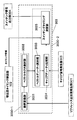
- FIG. 1E is a block diagram showing a schematic configuration of the AC conversion circuit of the present embodiment.
- the AC conversion circuit of this embodiment is configured to convert a single-phase input AC voltage having a frequency f0 into a three-phase output AC voltage having a relatively low frequency f1.
- the AC conversion circuit includes a switching unit 101 that outputs an input AC voltage to each phase by a plurality of switching elements, a zero-crossing timing detection unit 102 that detects a timing at which the value of the input AC voltage becomes 0 (zero-crossing timing), A switching control unit 103 that controls the operation of each switching element and a filter 104 that removes a high-frequency component of the output voltage of the switching unit 101 are provided.
- a load is connected to the subsequent stage of the filter 104, and an AC voltage having a frequency f1 is supplied to the load.
- the frequency f0 can be set to 100 kHz or more, for example, and the frequency f1 can be set to 50 Hz, which is the same as the frequency of the power system, for example.
- Both the input AC voltage and the output AC voltage are sine wave voltages.
- the input AC voltage can be, for example, a radio frequency (RF) voltage output from a power receiving unit of a wireless power transmission system using resonant magnetic field coupling.
- the switching unit 101 receives a single-phase AC voltage having a frequency f0.
- the switching unit 101 includes switching elements U, V, W, X, Y, and Z that operate based on a control signal input from the switching control unit 103. With these switching elements U, V, W, X, Y, and Z, the switching unit 101 outputs an input AC voltage to the subsequent filter 104 connected to each of the uv phase, the vw phase, and the wu phase. Switch between no.
- the uv phase, the vw phase, and the wu phase may be referred to as a u phase, a v phase, and a w phase, respectively.
- the switching elements U, V, W apply a positive voltage to the corresponding phase when the polarity of the input high-frequency alternating current is positive, and may be referred to as “first type switch” in this specification.
- the switching elements X, Y, and Z are switches that apply a positive voltage to a corresponding phase when the polarity of the input high-frequency alternating current is negative, and may be referred to as a “second type switch” in this specification.
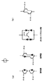
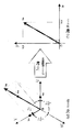
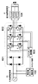
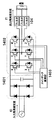
- FIG. 2 is a diagram illustrating a configuration example of each switching element.
- each switching element has a configuration in which a normal semiconductor switching element MOSFET or IGBT is connected in series or in parallel with a diode, or a configuration in which a diode bridge is connected.
- a control signal is input from the switching control unit 103 to the gate of each switching element.
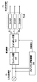
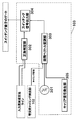
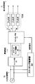
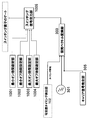
- FIG. 3A is a diagram illustrating a specific configuration of the switching control unit 103.
- the switching control unit 103 includes a reference sine wave generator 301 (reference signal generator) that generates a three-phase sine wave (reference signal) having the same frequency f1 as the output AC voltage of each phase, and the polarity (positive / negative) of the input AC voltage.
- reference sine wave generator 301 reference signal generator
- a space vector modulation unit 303 that generates a pulse train corresponding to each phase by space vector modulation, a switching signal output unit 304 that outputs a control signal input to the gate of each switching element, A carrier signal generation unit 305 that generates a signal (carrier signal) serving as a reference for determining a switching time in space vector modulation.
- pulse density modulation is performed using a modulation method called space vector modulation.
- Space vector modulation is disclosed in Patent Document 3 and Patent Document 4, for example. The entire disclosure of Patent Document 3 and Patent Document 4 is incorporated herein by reference.
- the space vector modulation unit 303 receives timing information indicating the timing at which the voltage value of the input AC voltage becomes 0 from the zero-crossing timing detection unit 102, and receives a carrier signal from the carrier signal generation unit 305. Moreover, the positive / negative determination part 302 is arrange
- the carrier signal output from the carrier signal generator 305 is, for example, a triangular wave having a frequency fc.
- the frequency fc of the carrier signal can be set higher than the frequency f1 of the reference signal output from the reference sine wave generator 301 and lower than the frequency f0 of the input high-frequency power.
- the frequency fc can be set to satisfy f1 ⁇ fc ⁇ f0.
- the output of the reference sine wave generation unit 301 is a sine wave that takes positive and negative values around zero.
- FIG. 3B is a diagram illustrating an example of a three-phase sine wave output from the reference sine wave generation unit 301. Since the three-phase sine wave voltages Vu, Vw, Vv correspond to the frequency and phase of the voltages to be output to the u-phase, v-phase, and w-phase, respectively, their amplitudes are equal to each other and the phase is 2 ⁇ / 3. It is shifted one by one.
- the sine waves Vu, Vv, and Vw can be expressed by the following formulas 1 to 3, respectively.
- the amplitude is A1
- the time when the phase of the sine wave voltage Vu corresponding to the u phase becomes 0 is the origin of the time coordinate.
- the origin of the time coordinate may be set at an arbitrary time.
- the space vector modulation unit 303 performs space vector modulation using the input three-phase sine wave voltage values Vu, Vv, and Vw as command values. Based on the carrier signal input from the carrier signal generation unit 305 and the timing information input from the zero crossing timing detection unit 102, the switching signal is output in synchronization with the timing when the voltage level of the input AC voltage becomes zero. Output to the unit 304.
- FIG. 3C is a diagram illustrating a configuration of the space vector modulation unit 303.
- the space vector modulation unit 303 includes a switching vector determination unit 3030-1 that determines a set of three vectors (switching vectors) that define a combination of switching elements to be conducted based on an input from the reference sine wave generation unit 301.
- a switching state determination unit 3030-2 for determining the time distribution (duty ratio) of the determined vector set and the timing of the conduction state represented by each vector.
- the switching vector determination unit 3030-1 includes a coordinate conversion unit 3031 that converts a three-dimensional vector having the value of the three-phase AC voltage input from the reference sine wave generation unit 301 into a two-dimensional vector, and a two-dimensional vector after conversion.
- a vector sector selection unit 3032 that determines three switching vectors by selecting a sector to which the vector belongs;
- the switching state determination unit 3030-2 includes a vector duty calculation unit 3033 that calculates the duty of the three switching vectors, a carrier duty comparison unit 3034 that compares the duty and the carrier signal, and switching based on each comparison vector based on the comparison result.
- a switching time determination unit 3035 for determining the time.
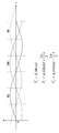
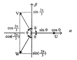
- FIG. 4 is a conceptual diagram of three-phase two-phase stationary coordinate transformation.
- the input values (three-phase balanced voltage instantaneous values) Vu, Vv, Vw from the reference sine wave generator 301 are divided into three axes U, V, Consider instantaneous vectors Vu, Vv, and Vw on W.
- the three-phase AC voltage input from the reference sine wave generator 301 that is, the voltage to be output to each phase can be expressed by a combined instantaneous vector Vs expressed by the following Equation 4.
- This combined instantaneous vector Vs is a vector having a constant magnitude that rotates at a constant angular frequency f1.
- this synthesized instantaneous vector is expressed by an ⁇ axis that coincides with the U axis and a ⁇ axis that is orthogonal thereto.
- the ⁇ component of Vs at this time is V ⁇
- the ⁇ component is V ⁇ .
- FIG. 5 is a diagram showing the relationship between the three-phase coordinate system and the two-phase coordinate system.
- FIG. 5 shows the size of the vectors on the U, V, and W axes when projected onto the ⁇ and ⁇ axes. From FIG. 5, V ⁇ and V ⁇ can be expressed by the following Equation 5.
- the coordinate conversion unit 3031 converts the command value of each phase into a three-phase two-phase static coordinate based on the above equation 6 using the input values (Vu, Vv, Vw) from the reference sine wave generation unit 301 as command values. By this conversion, the voltage value of the three-phase sine wave input from the reference sine wave generator 301 can be handled as a rotation vector having a constant magnitude.
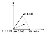
- FIG. 6 is a diagram in which eight vectors indicating selectable switching states are plotted on the coordinates represented by three axes U, V, and W whose angles are different from each other by 120 degrees on the plane, as in FIG. is there.
- these eight vectors are represented by V0 (0, 0, 0), V1 (1, 0, 0), V2 (1, 1, 0), V3 (0, 1, 0).
- V4 (0, 1, 1), V5 (0, 0, 1), V6 (1, 0, 1), V7 (1, 1, 1).
- V0 and V7 are zero vectors
- V1, V3, and V5 are vectors on the U, V, and W axes, respectively.
- the vectors V0 to V7 are called “switching vectors”.
- the vector sector selection unit 3032 selects which sector the command value vector Vs (V ⁇ , V ⁇ ) as shown in FIG. 4 converted by the coordinate conversion unit 3031 belongs, and forms a peripheral region of the selected sector 3 As a vector indicating a switching state to be set, the result is output to the vector duty calculation unit 3033.
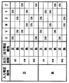
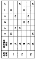
- the sector to which the command value vector Vs (V ⁇ , V ⁇ ) belongs is determined based on the phase ⁇ of the vector Vs as shown in Table 1.
- the phase ⁇ of the vector Vs is obtained by calculating the arc tangent (inverse tangent) of V ⁇ / V ⁇ .
- the vector duty calculation unit 3033 calculates the output time ratio (duty ratio) of the switching state represented by each vector based on the selection result input from the vector sector selection unit 3032.
- the method for determining each output time ratio will be described by taking the case where the input sector is 1 as an example.
- FIG. 7 is a diagram showing a command value vector Vs when the sector number is 1 and vectors forming its peripheral area.
- the vectors to be selected are V1 (1, 0, 0), V2 (1, 1, 0), and V0 (0, 0, 0).
- vector V7 (1, 1, 1) is also shown in FIG. 7, this vector means that power is output to all phases, and is not adopted in this embodiment.
- the command value vector Vs (V ⁇ , V ⁇ ) is represented by a linear combination of the vectors V0, V1, and V2.
- the output time ratio t0 of the vector V0 is 1 ⁇ (t1 + t2). That is, t0 can be calculated by obtaining t1 and t2.
- the relationship between the output time ratio of each vector and the element of the command value vector Vs can be expressed by the following Expression 7. If only the expressions relating to t1 and t2 are extracted from Expression 7, the following Expression 8 is obtained.
- the matrix A is defined as in Equation 9 below.
- t1 and t2 are expressed by the following formula 10 from Kramel's formula.
- is expressed by the following Expression 11.
- the carrier duty comparison unit 3034 normalizes the carrier signal input from the carrier signal generation unit 305 so as to have a value between 0 and 1 per cycle, and then inputs the duration ratio of each input switching state. Are compared, and the result is output to the switching time determination unit 3035.
- the zero-crossing timing detection unit 102 detects the timing when the voltage value of the input AC voltage becomes 0, and notifies the detected information to the space vector modulation unit 303 as timing information.
- the switching time determination unit 3035 determines the duration of each switching state based on the input comparison result and timing information.
- FIG. 8 is a diagram illustrating a generation principle of the switching signal by comparing the carrier signal with each duty ratio.
- the switching time determination unit 3035 compares each of t0, t1, and t2 taking values between 0 and 1 with a carrier having a control period Tc and an amplitude 1 (a triangular wave having a minimum value of 0 and a maximum value of 1). The timing for setting the switching state is determined. As shown in FIG. 8, the switching time determination unit 3035 first turns on / off each switching element so that a switching pattern corresponding to the vector V1 is obtained in a section where the output time ratio t1 is larger than the normalized carrier signal. Decide off.
- the setting timing is determined in the order of V1, V0, and V2, but the determination of the setting timing is not limited to this order.
- the order of vectors to be compared with the carrier signal can be determined in order from vectors that do not overlap in the time domain.
- the above comparison may be started from an appropriate vector, and the time domain corresponding to the condition may be selected from the time domain excluding the already determined time domain for the next vector.
- the setting timing of the conduction state represented by each switching vector can be determined by the same processing.
- the setting timing of each switching state is determined by comparing the carrier signal using a triangular wave and the output time ratio, but this is merely an example.
- the setting timing of each switching state may be determined by any method as long as the conduction state is determined according to the calculated duty ratio of each switching vector.
- the switching time determination unit 3035 synchronizes with the timing information input from the zero-crossing timing detection unit 102, and outputs each phase output shown in FIG. 8 as the final on / off time of each switching element.
- a pulse signal that lasts for a time obtained by multiplying the time ratio by the control period Tc of the carrier signal is output.
- the pulse signal output for each phase is input to the switching signal output unit 304.
- the pulse signal input to the switching signal output unit 304 has a continuous width.
- the switching signal output unit 304 updates the switching signal when the input AC voltage becomes zero, and quantizes (synchronizes) it with a half cycle of the input high-frequency voltage.
- a half cycle of the input high frequency power is converted into a signal for distributing to each phase and output as a control signal input to each switching element.
- the space vector modulation unit 303 outputs a pulse signal with a change in output time width having a frequency equal to the frequency f1 of the reference sine wave generation unit 301, so that the pulse signal passes through the switching element when the pulse signal is on.
- the density of the input high-frequency half-wave pulse changes at the frequency f1.
- the output AC voltage is a 50 Hz sine wave, but may be a waveform other than a sine wave.
- PDM Pulse Density Modulation
- the positive / negative determination unit 302 shown in FIG. 3A determines the current polarity of the input high-frequency AC voltage, and inputs the polarity information to the switching signal output unit 304.
- the switching signal output unit 304 is configured to switch on / off the switching elements of the switching unit 101 based on the pulse signal output from the space vector modulation unit 303 and the polarity information output from the positive / negative determination unit 302. Output a control signal.
- FIG. 9 is a correspondence table showing what control signal the switching signal output unit 304 outputs for the combination of the polarity of the input AC voltage and the polarity of the output voltage to be output to each phase.
- the input voltage polarity indicates the polarity information received from the positive / negative determination unit 302
- the output voltage polarity indicates the polarity of the three-phase AC voltage output from the reference sine wave generation unit 301.
- the switching signal output unit 304 applies a positive polarity voltage between the uv phases
- the switching elements U and Y are simultaneously turned on and the input voltage polarity is negative.
- the switching elements V and X are simultaneously turned on.
- the switching signal output unit 304 switches the switching elements U, V, W, X, Y, and Z on and off according to this correspondence table
- the voltage corresponding to 1 ⁇ 2 wavelength of the input AC voltage is one pulse.
- the pulses are distributed to each phase so that the change in pulse density per unit time becomes a three-phase sine wave.
- the switching control unit 103 exclusively controls the pair of switching elements U and X, V and Y, and W and Z so as not to be turned on at the same time in order to prevent a short circuit on the output side.
- the correspondence table shown in FIG. 9 is recorded in, for example, a memory (not shown) as a table, and the above control can be realized by the switching control unit 103 referring to the table.
- the circuit configuration of the switching control unit 103 may be designed in advance so as to perform the operations shown in the correspondence table.
- the switching unit 101 outputs a pulse train having a voltage corresponding to a half wavelength of the input AC voltage as one pulse.
- the output pulse train is input to the filter 104 arranged for each phase.
- Each filter 104 removes a high-frequency component from the output pulse train sent from the switching unit 101, and outputs a low-frequency AC voltage of 50 Hz as a final output.
- the filter 104 is a low-pass filter composed of an inductor and a capacitor.
- the cutoff frequency of the filter is f0 / (10 ⁇ n). If set to, harmonic noise can be effectively removed. For example, when f0 is 100 kHz and the three-phase output is performed, the cut-off frequency may be set to about 33.3 kHz.
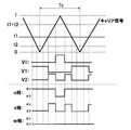
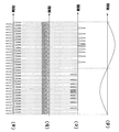
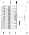
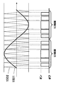
- FIG. 10 is a diagram showing the relationship between the input high-frequency AC voltage, the output of the switching unit 101, and the output waveform of a certain one-phase filter 104.
- FIG. 10A shows the change over time of the input high-frequency AC voltage having the frequency f0.
- FIG. 10B shows an example of the time change of the output of the switching unit 101. Since ON / OFF of the switch is controlled in synchronization with the output of the ⁇ - ⁇ converter at the zero crossing timing of the input AC voltage, a pulse train whose density changes sinusoidally is output.
- FIG. 10C shows an example of the time change of the output of the filter 104.
- the density change in the output of the switching unit 101 is a sine wave having a frequency of 50 Hz
- an AC voltage having a frequency of 50 Hz is output from the filter 104.
- the input high-frequency AC voltage can be directly converted into a 50-Hz low-frequency AC voltage without being converted into a DC voltage. Thereby, highly efficient power conversion becomes possible.
- AC power with a relatively high frequency is converted into AC power with a relatively low frequency by pulse density modulation based on space vector modulation and output.
- pulse density modulation based on space vector modulation and output.
- a sector is determined based on the phase of a vector defined by three reference sine waves, and the conduction state of each switching element is controlled using the three switching vectors constituting the determined sector. Is done.
- the vector transition angle due to the switching transition is always kept within 30 degrees. For example, compared to the case where pulse density modulation by ⁇ - ⁇ modulation is used, reverse current generation, output voltage sticking (clamping), etc. This can be suppressed, and a decrease in conversion efficiency can be prevented.
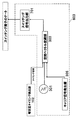
- FIG. 11 is a block diagram showing a schematic configuration of an AC conversion circuit in the present embodiment.
- the AC converter circuit of the present embodiment includes a converter unit 601 that performs a rectifying action before the switching unit 602, and is different from the AC converter circuit of the first embodiment in that an input AC voltage is once converted into a DC voltage.
- the description will focus on the differences from the first embodiment, and a description of the overlapping items will be omitted.
- the AC converter circuit includes a converter unit 601 that converts an AC voltage into a DC voltage, a switching unit 602 that converts an input DC voltage and outputs it to each phase, and the value of the input AC voltage becomes zero.
- a zero-crossing timing detection unit 102 that detects timing
- a switching control unit 603 that controls the operation of each switching element
- a filter 104 that removes a high-frequency component of the output voltage of the switching unit 101 are provided.
- a load is connected to the subsequent stage of the filter 104, and an AC voltage having a frequency f1 is supplied to the load.
- the frequency f0 is set to 100 kHz or more, for example, and the frequency f1 is set to 50 Hz, which is the same as the frequency of the power system, for example.
- Both the input AC voltage and the output AC voltage are sine wave voltages.
- the converter unit 601 is configured by a diode bridge, rectifies an input frequency f0 and a single-phase AC voltage, and generates a positive pulse train having a frequency of 2f0 with a voltage corresponding to 1 ⁇ 2 wavelength of the AC voltage as one pulse. Convert.
- the switching unit 602 includes switching elements U, V, W, X, Y, and Z that operate based on a control signal input from the switching control unit 603, and is connected to each phase of u, v, and w. Whether to output the input pulse train to the subsequent filter 104 is switched.
- each switching element is configured by a MOSFET or IGBT which is a normal semiconductor switching element.
- the output of the switching control unit 603 is input to the gate of each switching element.
- FIG. 12 is a diagram illustrating a specific configuration of the switching control unit 603.
- the switching control unit 603 includes a reference sine wave generation unit 301, a space vector modulation unit 303, and a switching signal output unit 701.
- the zero-crossing timing detection unit 102 detects the timing when the voltage value of the input AC voltage becomes 0, and notifies the detected information to the space vector modulation unit 303 as timing information.
- the reference sine wave generation unit 301 generates a 50 Hz three-phase sine wave whose phase is shifted by 120 degrees with power sufficiently smaller than the input high-frequency AC power, and is input to the space vector modulation unit 303 for each phase.
- the space vector modulation unit 303 performs space vector modulation similar to that of the first embodiment using the input sine wave values of the respective phases as command values.
- a pulse is sent to the switching signal output unit 701 in synchronization with the timing when the voltage level of the input AC voltage becomes 0 based on the timing information.
- the on-time change of the pulse output is a 50 Hz sine wave having the same period as the sine wave from the reference sine wave generator 301.
- the switching signal output unit 701 outputs a control signal for switching on and off to each switching element of the switching unit 602 based on the input from the space vector modulation unit 303.
- FIG. 13 is a correspondence table showing what kind of control signal the switching signal output unit 701 outputs with respect to the output voltage polarity of each phase in the present embodiment. For example, when a positive polarity voltage is applied to the uv phase, the switching signal output unit 701 turns on the switching elements U and Y at the same time, and applies a negative polarity voltage between the uv phases. The switching elements V and X are turned on simultaneously. Further, preferably, in order to prevent a short circuit on the output side, the switching elements U and X, V and Y, and W and Z are controlled exclusively so that they are not simultaneously turned on. As described above, the switching control unit 603 performs PDM modulation by performing space vector modulation on the pulse train output from the converter unit 601.
- Each filter 104 removes a high frequency component from the output pulse train sent from the switching unit 602, and outputs a low frequency AC voltage of 50 Hz as a final output.
- the input high-frequency alternating current is converted into a half-wave train that is PDM modulated by the switching unit 602. Converted.
- the PDM-modulated half-wave train is finally converted into low-frequency alternating current by low-pass filtering by the filter 104 as shown in FIG.
- the zero-crossing timing detection unit 102 detects the timing when the input high-frequency AC voltage is zero, but may be configured to detect the timing when the output voltage of the converter unit 601 is zero.
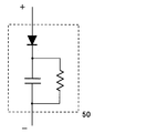
- FIG. 16 is an example of a specific configuration diagram of the clamp snubber circuit 50.
- a diode connected in the forward direction from the positive voltage to the negative voltage, and a capacitor and a resistor connected in series to the diode are connected in parallel. Filter. As a result, it is possible to suppress oscillation associated with a large voltage change that occurs during switching, and to reduce loss that occurs during switching.
- FIG. 17 is a diagram showing a schematic configuration of a switching control unit of the AC conversion circuit in the present embodiment.
- the switching control unit in this embodiment further includes a minimum on-time setting unit 1001, a minimum off-time setting unit 1002, a maximum on-time setting unit 1003, and a maximum off-time setting unit 1004.
- the minimum on time setting unit 1001 sends the minimum time that each switching element is continuously turned on to the switching signal output unit 1005 as switching time information.
- the minimum time is an integral multiple of one half of the cycle (1 / f0) of the input high-frequency AC voltage. Is set. The minimum time may be set in advance, or may be adjusted by the user by looking at the output state of the AC conversion circuit.
- the minimum off time setting unit 1002 sets the minimum time that each switching element is continuously turned off, and the maximum on time setting unit 1003 sets the maximum time that each switching element is continuously turned on.
- the off time setting unit 1004 sends the maximum time that the switching element is continuously turned off to the switching signal output unit 1005 as switching time information.
- the switching signal output unit 1005 is for controlling on / off of each switching element based on the set minimum and maximum values of the on-time and off-time of each switching element and the output of the space vector modulation unit 303. Output a control signal.
- FIG. 18 shows that the frequency of the high-frequency alternating current input to the converter unit 601 is f0 Hz, the frequency of the output low-frequency alternating current is foutHz, and the minimum on-time and minimum off-time are 1 / f0 seconds (one cycle of the input high-frequency alternating current).
- the switching signal output unit 1005 does not completely follow the output pulse from the space vector modulation unit 303, and once the switching element is turned on or off, the switching state is changed for a preset minimum time. maintain. However, each switching element is controlled so that the final output is as close as possible to the sine wave reflecting the density change of the output pulses from the space vector modulation unit 303.
- the number of times of switching can be reduced compared to the case where switching is performed with the time corresponding to one output half wave of the converter unit 601 as the minimum time unit. For this reason, the loss of the electric power for switching drive and the electric power accompanying switching can be reduced, and an output low frequency alternating current can be obtained efficiently.
- the minimum on-time and the minimum off-time have the same value has been described as an example, but each value may be different.
- the loss becomes smaller as the number of times of switching becomes smaller, the loss can be reduced as the minimum on time and the minimum off time are lengthened.
- increasing the minimum on-time and the minimum off-time has the same effect as decreasing the number of PDM modulations performed by the space vector modulation unit 303 as a result. That is, the smoothness of the density change of the output half-wave of the switching unit 602 is reduced, which may cause waveform distortion of the final output low-frequency alternating current.
- the maximum on-time and the maximum off-time are further set, and the duration of the on-time and off-time is within the preset time. Limited. With such a configuration, loss due to switching can be reduced without causing waveform distortion in the final output low-frequency alternating current.
- a minimum on-time setting unit 1001, a minimum off-time setting unit 1002, a maximum on-time setting unit 1003, and a maximum off-time setting unit 1004 are provided, but only some of them are provided. It may be done.
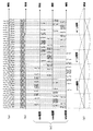
- control may be performed so that the half-circumference of the input high-frequency alternating current is always output to only one phase at any time.
- FIG. 4 is a diagram showing output waveforms of the filter 104 of each phase. As shown in FIG. 19, at any time, the half cycle of the input high-frequency alternating current is always output in only one phase.
- the uv phase, the vw phase, and the wu phase are controlled so that the number of output half waves per cycle of the input AC voltage is the same.
- each component of the AC conversion circuit is represented as a separate functional unit that is blocked.
- the AC conversion is performed by causing the processor to execute a program that defines the processing of these functional units.
- the operation of the circuit may be realized.
- Such a program can be recorded on a recording medium such as a CD-ROM, a DVD-ROM, or a flash memory, or can be distributed through an electric communication line such as the Internet or an intranet.
- Switching part 30 Switching control part 40 Converter part 50 Clamp snubber circuit 101 Switching part 102 Zero crossing timing detection part 103 Switching control part 104 Low-pass filter part (filter) 301 Reference Sine Wave Generation Unit 302 Positive / Negative Determination Unit 303 Space Vector Modulation Unit 304 Switching Signal Output Unit 3030-1 Switching Vector Determination Unit 3030-2 Switching State Determination Unit 3031 Coordinate Conversion Unit 3032 Vector Sector Selection Unit 3033 Vector Duty Calculation Unit 3034 Carrier Duty comparison unit 3035 Switching time determination unit 305 Carrier signal generation unit 601 Converter unit 602 Switching unit 603 Switching control unit 701 Switching signal output unit 1001 Minimum on-time setting unit 1002 Minimum off-time setting unit 1003 Maximum on-time setting unit 1004 Maximum off-time Setting unit 1403 Switching control unit 1501 Reference sine wave 1502 Triangular wave
Abstract
Priority Applications (4)
| Application Number | Priority Date | Filing Date | Title |
|---|---|---|---|
| EP12850960.1A EP2784924B1 (fr) | 2011-11-22 | 2012-11-15 | Circuit de conversion de c.a. |
| JP2013518888A JP5996531B2 (ja) | 2011-11-22 | 2012-11-15 | 交流変換回路 |
| CN201280006122.0A CN103339845B (zh) | 2011-11-22 | 2012-11-15 | 交流变换电路 |
| US14/008,709 US9190925B2 (en) | 2011-11-22 | 2012-11-15 | AC converter for converting a single-phase input AC voltage into a three-phase output AC voltage |
Applications Claiming Priority (2)
| Application Number | Priority Date | Filing Date | Title |
|---|---|---|---|
| JP2011-254791 | 2011-11-22 | ||
| JP2011254791 | 2011-11-22 |
Publications (1)
| Publication Number | Publication Date |
|---|---|
| WO2013076937A1 true WO2013076937A1 (fr) | 2013-05-30 |
Family
ID=48469405
Family Applications (1)
| Application Number | Title | Priority Date | Filing Date |
|---|---|---|---|
| PCT/JP2012/007333 WO2013076937A1 (fr) | 2011-11-22 | 2012-11-15 | Circuit de conversion de c.a. |
Country Status (5)
| Country | Link |
|---|---|
| US (1) | US9190925B2 (fr) |
| EP (1) | EP2784924B1 (fr) |
| JP (1) | JP5996531B2 (fr) |
| CN (1) | CN103339845B (fr) |
| WO (1) | WO2013076937A1 (fr) |
Families Citing this family (8)
| Publication number | Priority date | Publication date | Assignee | Title |
|---|---|---|---|---|
| WO2014020703A1 (fr) * | 2012-07-31 | 2014-02-06 | 株式会社安川電機 | Convertisseur de matrice |
| DE102014108667A1 (de) * | 2014-06-20 | 2015-12-24 | Technische Universität Braunschweig | Stromrichter und Computerprogramm |
| KR101628920B1 (ko) * | 2014-07-31 | 2016-06-10 | 고려대학교 산학협력단 | 전력계통 주파수 유연화 운영 시스템 및 그 방법 |
| CN105429447A (zh) * | 2015-12-21 | 2016-03-23 | 华南理工大学 | 一种共模抑制双Boost倍压PFC变换器 |
| JPWO2019188876A1 (ja) * | 2018-03-29 | 2021-03-25 | パナソニックIpマネジメント株式会社 | 電力変換システム、電圧変換回路の制御方法 |
| US10158299B1 (en) * | 2018-04-18 | 2018-12-18 | Rockwell Automation Technologies, Inc. | Common voltage reduction for active front end drives |
| DE102018210391A1 (de) * | 2018-06-26 | 2020-01-02 | Schmidhauser Ag | Verfahren zum Betreiben eines Wechselrichters und Wechselrichter |
| US11211879B2 (en) | 2019-09-23 | 2021-12-28 | Rockwell Automation Technologies, Inc. | Capacitor size reduction and lifetime extension for cascaded H-bridge drives |
Citations (6)
| Publication number | Priority date | Publication date | Assignee | Title |
|---|---|---|---|---|
| JPH0479770A (ja) | 1990-07-20 | 1992-03-13 | Toshiba Corp | インバータ装置の三相pwm信号発生回路 |
| JPH11346478A (ja) | 1998-06-01 | 1999-12-14 | Fuji Electric Co Ltd | 電圧形インバータ |
| JP2000324853A (ja) * | 1999-04-30 | 2000-11-24 | Texas Instr Inc <Ti> | 電源インバータにおけるdcバス・リップル作用を減少させるモディファイド空間ベクトル・パルス幅変調方法及び装置 |
| JP2008048530A (ja) * | 2006-08-15 | 2008-02-28 | Meidensha Corp | 交流−交流直接変換装置の空間ベクトル変調方法 |
| US20080278264A1 (en) | 2005-07-12 | 2008-11-13 | Aristeidis Karalis | Wireless energy transfer |
| JP2009501510A (ja) * | 2005-07-12 | 2009-01-15 | マサチューセッツ インスティテュート オブ テクノロジー | 無線非放射型エネルギー転送 |
Family Cites Families (17)
| Publication number | Priority date | Publication date | Assignee | Title |
|---|---|---|---|---|
| DE69127664T2 (de) | 1990-07-20 | 1998-02-12 | Toshiba Kawasaki Kk | Vorrichtung zur Erzeugung eines dreiphasigen PWM-Signals für Wechselrichter |
| DE19823917A1 (de) * | 1997-06-03 | 1998-12-10 | Fuji Electric Co Ltd | Stromrichtervorrichtung |
| JPH1198837A (ja) * | 1997-09-24 | 1999-04-09 | Sansha Electric Mfg Co Ltd | 直流電源装置 |
| DE10146527A1 (de) * | 2001-09-21 | 2003-04-24 | Siemens Ag | Umrichter mit einem netz- und lastseitigen selbstgeführten Pulsstromrichter |
| US6653812B1 (en) * | 2002-01-31 | 2003-11-25 | Analog Devices, Inc. | Space vector modulation methods and structures for electric-motor control |
| CN1303753C (zh) * | 2005-06-07 | 2007-03-07 | 南京工业大学 | 交流异步电机的无速度传感器逆控制器 |
| US7599196B2 (en) * | 2006-06-06 | 2009-10-06 | Ideal Power Converters, Inc. | Universal power converter |
| JP4192979B2 (ja) * | 2006-08-31 | 2008-12-10 | ダイキン工業株式会社 | モータ制御装置 |
| CN100433536C (zh) * | 2007-01-15 | 2008-11-12 | 南京航空航天大学 | 基于电压空间矢量的调制方法 |
| WO2009028053A1 (fr) * | 2007-08-29 | 2009-03-05 | Mitsubishi Electric Corporation | Convertisseur ca/cc et unité d'entraînement du compresseur et conditionneur d'air comprenant ce dernier |
| US7616466B2 (en) * | 2007-09-12 | 2009-11-10 | Gm Global Technology Operations, Inc. | Three phase inverter with improved loss distribution |
| CN101295935B (zh) * | 2007-12-10 | 2010-06-02 | 西北工业大学 | 一种可抑制谐波的优化pwm调制方法 |
| MY157433A (en) * | 2008-07-24 | 2016-06-15 | Panasonic Corp | Power conversion apparatus |
| KR101297545B1 (ko) * | 2009-01-19 | 2013-08-14 | 다이킨 고교 가부시키가이샤 | 양방향 스위치회로 및 이를 구비한 전력변환장치 |
| ES2899877T3 (es) * | 2009-12-24 | 2022-03-15 | Mitsubishi Electric Corp | Aparato de conversión de potencia y método de accionamiento para aparato de conversión de potencia |
| US8659238B2 (en) * | 2011-04-20 | 2014-02-25 | Xi' An Upright Photoelectric Technology Co., Ltd | Switching power supply with power feedback to keep lamp's brightness constant |
| CN103038993B (zh) * | 2011-05-26 | 2016-04-20 | 松下电器产业株式会社 | 交流变换电路、交流变换方法及记录介质 |
-
2012
- 2012-11-15 JP JP2013518888A patent/JP5996531B2/ja active Active
- 2012-11-15 WO PCT/JP2012/007333 patent/WO2013076937A1/fr active Application Filing
- 2012-11-15 EP EP12850960.1A patent/EP2784924B1/fr active Active
- 2012-11-15 US US14/008,709 patent/US9190925B2/en active Active
- 2012-11-15 CN CN201280006122.0A patent/CN103339845B/zh active Active
Patent Citations (7)
| Publication number | Priority date | Publication date | Assignee | Title |
|---|---|---|---|---|
| JPH0479770A (ja) | 1990-07-20 | 1992-03-13 | Toshiba Corp | インバータ装置の三相pwm信号発生回路 |
| JPH11346478A (ja) | 1998-06-01 | 1999-12-14 | Fuji Electric Co Ltd | 電圧形インバータ |
| JP2000324853A (ja) * | 1999-04-30 | 2000-11-24 | Texas Instr Inc <Ti> | 電源インバータにおけるdcバス・リップル作用を減少させるモディファイド空間ベクトル・パルス幅変調方法及び装置 |
| US6313602B1 (en) | 1999-04-30 | 2001-11-06 | Texas Instruments Incorporated | Modified space vector pulse width modulation technique to reduce DC bus ripple effect in voltage source inverters |
| US20080278264A1 (en) | 2005-07-12 | 2008-11-13 | Aristeidis Karalis | Wireless energy transfer |
| JP2009501510A (ja) * | 2005-07-12 | 2009-01-15 | マサチューセッツ インスティテュート オブ テクノロジー | 無線非放射型エネルギー転送 |
| JP2008048530A (ja) * | 2006-08-15 | 2008-02-28 | Meidensha Corp | 交流−交流直接変換装置の空間ベクトル変調方法 |
Also Published As
| Publication number | Publication date |
|---|---|
| US20140056038A1 (en) | 2014-02-27 |
| CN103339845A (zh) | 2013-10-02 |
| JP5996531B2 (ja) | 2016-09-21 |
| US9190925B2 (en) | 2015-11-17 |
| EP2784924A4 (fr) | 2016-03-02 |
| EP2784924B1 (fr) | 2018-11-07 |
| EP2784924A1 (fr) | 2014-10-01 |
| JPWO2013076937A1 (ja) | 2015-04-27 |
| CN103339845B (zh) | 2017-02-08 |
Similar Documents
| Publication | Publication Date | Title |
|---|---|---|
| JP5996531B2 (ja) | 交流変換回路 | |
| JP4139852B1 (ja) | インバータ制御装置 | |
| Nguyen et al. | Dual three-phase indirect matrix converter with carrier-based PWM method | |
| JP5304937B2 (ja) | 電力変換装置 | |
| JP4488122B2 (ja) | 電力変換器及びその制御方法並びにダイレクトマトリックスコンバータ | |
| JP5970173B2 (ja) | 交流変換回路、交流変換方法、およびプログラム | |
| JP5047582B2 (ja) | インバータ装置 | |
| JP4793484B2 (ja) | 共振型コンバータ装置 | |
| JP5551833B2 (ja) | 電力変換制御装置、電力変換制御方法、電動機および車両駆動システム | |
| WO2016158805A1 (fr) | Convertisseur matriciel triphasé/monophasé | |
| TWI667874B (zh) | Power conversion device and three-phase AC power supply device | |
| JP2010068552A (ja) | 交流直流変換装置及び交流直流変換装置の制御方法並びにヒートポンプ式給湯器及び空気調和機 | |
| JP2007306676A (ja) | 交流−交流直接変換装置のスイッチングパターン生成方法 | |
| JP2021027672A (ja) | 電子回路および無線電力伝送装置 | |
| JP2019004616A (ja) | インバータ装置、空気調和機、インバータ装置の制御方法及びプログラム | |
| JP2007006564A (ja) | 交流−交流直接電力変換器の制御装置 | |
| JP2018164347A (ja) | インバータ装置、空気調和機、インバータ装置の制御方法及びプログラム | |
| JP5506619B2 (ja) | インバータ装置及び制御方法 | |
| JP2019004617A (ja) | インバータ装置、空気調和機、インバータ装置の制御方法及びプログラム | |
| JP2020102933A (ja) | スイッチング電源装置及びその制御方法 | |
| JP5929080B2 (ja) | 電力変換装置 | |
| JP2014147294A (ja) | 電力変換制御装置、電動機および車両駆動システム |
Legal Events
| Date | Code | Title | Description |
|---|---|---|---|
| ENP | Entry into the national phase |
Ref document number: 2013518888 Country of ref document: JP Kind code of ref document: A |
|
| 121 | Ep: the epo has been informed by wipo that ep was designated in this application |
Ref document number: 12850960 Country of ref document: EP Kind code of ref document: A1 |
|
| WWE | Wipo information: entry into national phase |
Ref document number: 14008709 Country of ref document: US |
|
| WWE | Wipo information: entry into national phase |
Ref document number: 2012850960 Country of ref document: EP |
|
| NENP | Non-entry into the national phase |
Ref country code: DE |