WO2013069362A1 - 発熱点検出方法及び発熱点検出装置 - Google Patents
発熱点検出方法及び発熱点検出装置 Download PDFInfo
- Publication number
- WO2013069362A1 WO2013069362A1 PCT/JP2012/072223 JP2012072223W WO2013069362A1 WO 2013069362 A1 WO2013069362 A1 WO 2013069362A1 JP 2012072223 W JP2012072223 W JP 2012072223W WO 2013069362 A1 WO2013069362 A1 WO 2013069362A1
- Authority
- WO
- WIPO (PCT)
- Prior art keywords
- integrated circuit
- frequency
- unit
- electrical signal
- heat generation
- Prior art date
- Legal status (The legal status is an assumption and is not a legal conclusion. Google has not performed a legal analysis and makes no representation as to the accuracy of the status listed.)
- Ceased
Links
Images


Classifications
-
- G—PHYSICS
- G01—MEASURING; TESTING
- G01K—MEASURING TEMPERATURE; MEASURING QUANTITY OF HEAT; THERMALLY-SENSITIVE ELEMENTS NOT OTHERWISE PROVIDED FOR
- G01K13/00—Thermometers specially adapted for specific purposes
-
- G—PHYSICS
- G01—MEASURING; TESTING
- G01N—INVESTIGATING OR ANALYSING MATERIALS BY DETERMINING THEIR CHEMICAL OR PHYSICAL PROPERTIES
- G01N25/00—Investigating or analyzing materials by the use of thermal means
- G01N25/72—Investigating presence of flaws
-
- G—PHYSICS
- G01—MEASURING; TESTING
- G01K—MEASURING TEMPERATURE; MEASURING QUANTITY OF HEAT; THERMALLY-SENSITIVE ELEMENTS NOT OTHERWISE PROVIDED FOR
- G01K17/00—Measuring quantity of heat
-
- G—PHYSICS
- G01—MEASURING; TESTING
- G01R—MEASURING ELECTRIC VARIABLES; MEASURING MAGNETIC VARIABLES
- G01R31/00—Arrangements for testing electric properties; Arrangements for locating electric faults; Arrangements for electrical testing characterised by what is being tested not provided for elsewhere
- G01R31/28—Testing of electronic circuits, e.g. by signal tracer
- G01R31/2851—Testing of integrated circuits [IC]
- G01R31/2855—Environmental, reliability or burn-in testing
- G01R31/2872—Environmental, reliability or burn-in testing related to electrical or environmental aspects, e.g. temperature, humidity, vibration, nuclear radiation
- G01R31/2874—Environmental, reliability or burn-in testing related to electrical or environmental aspects, e.g. temperature, humidity, vibration, nuclear radiation related to temperature
- G01R31/2875—Environmental, reliability or burn-in testing related to electrical or environmental aspects, e.g. temperature, humidity, vibration, nuclear radiation related to temperature related to heating
-
- G—PHYSICS
- G01—MEASURING; TESTING
- G01R—MEASURING ELECTRIC VARIABLES; MEASURING MAGNETIC VARIABLES
- G01R31/00—Arrangements for testing electric properties; Arrangements for locating electric faults; Arrangements for electrical testing characterised by what is being tested not provided for elsewhere
- G01R31/28—Testing of electronic circuits, e.g. by signal tracer
- G01R31/302—Contactless testing
- G01R31/308—Contactless testing using non-ionising electromagnetic radiation, e.g. optical radiation
- G01R31/311—Contactless testing using non-ionising electromagnetic radiation, e.g. optical radiation of integrated circuits
Definitions
- the present invention relates to a heating point detection method and a heating point detection device for detecting the depth of a heating point of an integrated circuit.
- Non-Patent Document 1 describes that a phase difference ⁇ between electrical excitation and local thermal response is detected, and the depth of the defect is determined from the phase difference ⁇ .
- the amount of heat generation varies depending on the magnitude of the excitation signal and the state of the defect point
- the heat capacity between the defect point and the surface of the integrated circuit varies depending on the position of the defect point.
- the defect point depth it depends on the amount of heat generation, the structure of the integrated circuit and the position of the defect point.
- the position dependency of the offset of the phase difference is generated when the heat transfer coefficient from the surface of the integrated circuit as a sample to the air is determined by the temperature of the surface and the state of convection on the surface.
- the temperature rise of the sample is a factor of the error of the phase difference offset. That is, when the thermal response is acquired, the temperature of the sample continuously rises, and the inclination accompanying the temperature rise is detected as another wave. As a result, there is a tendency that an accurate phase difference cannot be detected.
- the present invention has been made in view of the above problems, and a heating point detection method and a heating point detection device capable of detecting the depth of a heating point in an integrated circuit accurately and stably without depending on the position.
- the purpose is to provide.
- a heating point detection method for detecting the depth of a heating point of an integrated circuit, and stabilizes the average temperature of the surface of the integrated circuit.
- a heating point detection device is a heating point detection device that detects the depth of a heating point of an integrated circuit, and includes an electrical signal supply unit that supplies an electrical signal to the integrated circuit, and an integrated circuit.
- a control unit that controls the electrical signal supply unit to supply the circuit with a periodic electrical signal that increases and decreases at a first frequency and a periodic electrical signal that increases and decreases at a second frequency different from the first frequency; Acquiring a first detection signal indicating a change in the amount of heat detected from the integrated circuit in response to the supply of a periodic electrical signal of a second frequency, and the integrated circuit in response to the supply of a periodic electrical signal of a second frequency
- a detection unit that obtains a second detection signal indicating a change in the amount of heat detected from the calculation unit, a calculation unit that obtains depth information of the heating point based on the first and second detection signals, and a surface of the integrated circuit
- a temperature stabilization unit that stabilizes the average temperature. .
- a heating point detection method or a heating point detection device in response to the supply of the periodic electrical signal having the first frequency from the integrated circuit with the average temperature of the surface of the integrated circuit being stabilized.
- a first detection signal indicating a change in the amount of heat generation is detected
- a second detection signal indicating a change in the amount of heat generation according to the supply of the periodic electrical signal having the second frequency is detected.
- depth information of the heating point is obtained.
- the depth information is calculated based on the thermal response to the electric signals of the two frequencies detected after the average temperature of the surface of the integrated circuit is stabilized at a constant (substantially constant). Highly accurate depth information can be obtained stably without depending on the position of the.
- the depth of the heat generation point in the integrated circuit can be detected accurately and stably without depending on the position.
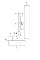
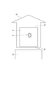
- FIG. 1 is a block diagram showing a schematic configuration of an integrated circuit failure analysis apparatus according to a preferred embodiment of the present invention. It is a side view which shows an example of a structure of the temperature stabilization part of FIG. It is a top view which shows the discharge
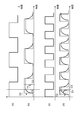
- (A) is a time change of a bias voltage
- (b) is a time change of the heat generation detection signal detected in the integrated circuit S made of a material having a low heat capacity / low heat transfer rate
- (c) is a high heat capacity / high heat transfer. It is a figure which shows the time change of the heat_generation
- FIG. 4D is a diagram showing a time change of a heat generation detection signal detected in the integrated circuit S.
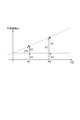
- FIG. 2 is a graph showing a relationship between a square root of an angular frequency of a bias voltage applied to an integrated circuit S and an observed phase delay bx in the integrated circuit failure analysis apparatus of FIG. It is a side view which shows an example of a structure of the temperature stabilization part of the modification of this invention.
- FIG. 1 is a block diagram showing a schematic configuration of an integrated circuit failure analysis device which is a heating point detection device according to a preferred embodiment of the present invention.
- An integrated circuit failure analysis apparatus 1 shown in FIG. 1 is a failure analysis apparatus that detects a position of a heating point of an integrated circuit S such as an LSI or an IC and performs failure analysis.
- the integrated circuit failure analysis apparatus 1 includes a sample stage 10, a stage drive unit 12 that drives the sample stage 10, a voltage application unit (electric signal supply unit) 14, an imaging device 18, a control unit 20, and image processing.
- the unit 30 and the temperature stabilization unit 40 are provided.
- the integrated circuit S to be analyzed is placed on a sample stage 10 using an XYZ stage that can be driven in the X-axis direction, the Y-axis direction (horizontal direction), and the Z-axis direction (vertical direction).
- the sample stage 10 is configured to be driven in the X, Y, and Z directions by the stage driving unit 12, and thereby, focusing of the imaging with respect to the integrated circuit S, positioning of the imaging position, and the like are performed.
- an imaging device 18 that is an imaging means for acquiring a two-dimensional image of the integrated circuit S is installed.
- an imaging device having sensitivity in a predetermined wavelength region for example, an infrared imaging device having sensitivity in the wavelength region of infrared light is suitable for acquiring an image based on a heat generation image on the surface of the integrated circuit S.
- the surface of the integrated circuit S refers to an observation surface on which an image is acquired by the imaging device 18.
- a light guide optical system 16 such as an objective lens that guides an image of the surface of the integrated circuit S to the image pickup device 18 is provided on the optical axis between the sample stage 10 and the image pickup device 18.
- the light guide optical system 16 may be provided with a driving mechanism such as an XYZ stage, and the driving mechanism may be capable of focusing on the integrated circuit S, aligning the imaging position, and the like.
- the voltage application unit 14 that supplies a voltage signal to the integrated circuit S on the sample stage 10 is provided.
- the voltage application unit 14 is a voltage application unit that applies a necessary bias voltage to an electronic circuit in the integrated circuit S when performing failure analysis by detecting a heating point, and includes a power supply for voltage application. ing. Specifically, the voltage application unit 14 applies a voltage signal (periodic electrical signal) that is a rectangular wave that periodically increases and decreases as the bias voltage. Thereby, a high voltage and a low voltage are periodically applied to the integrated circuit S.
- the voltage application unit 14 is configured to be able to change the frequency (repetition cycle) of the bias voltage to be applied under the control of the control unit 20.
- the voltage application unit 14 is configured to be able to change the high voltage value and the low voltage value of the bias voltage to be applied under the control of the control unit 20.
- the imaging device 18 acquires a plurality of analysis images in a time series in a state where a bias voltage is applied to the integrated circuit S by the voltage application unit 14.
- the analysis image acquired in this way is an image including a heat generation image of the surface of the integrated circuit S.
- the imaging frequency (frame rate) of the imaging device 18 may be set based on the frequency of the bias voltage applied to the integrated circuit S by the voltage application unit 14.
- the imaging frequency of the imaging device 18 may be the same period as the frequency of the bias voltage applied to the integrated circuit S, or may be set to be proportional to the frequency of the bias voltage. Thereby, even if the frequency of the bias voltage is different, a heat generation image in a relatively same heat generation state can be acquired.
- the integrated circuit failure analysis apparatus 1 includes a control unit 20 that controls operations of the sample stage 10, the stage driving unit 12, the voltage application unit 14, the light guide optical system 16, and the imaging device 18. Is provided.
- the control unit 20 includes an imaging control unit 21, a stage control unit 22, and a synchronization control unit 23.
- the imaging control unit 21 controls the acquisition of the analysis image of the integrated circuit S by controlling the bias voltage application operation by the voltage application unit 14 and the image acquisition operation by the imaging device 18. Further, the stage control unit 22 controls the operations of the sample stage 10 and the stage driving unit 12 (the movement operation of the integrated circuit S on the sample stage 10). In addition, the synchronization control unit 23 performs control for obtaining necessary synchronization between the imaging control unit 21 and the stage control unit 22 and the image processing unit 30 provided for the imaging device 18. That is, the synchronization control unit 23 controls the stage control unit 22 to move to a predetermined position for performing the failure analysis of the integrated circuit S, and then sequentially changes the frequency of the bias voltage at predetermined intervals. The imaging control unit 21 is controlled.
- the synchronization control unit 23 controls the high voltage value and the low voltage value of the periodically applied bias voltage. In addition, the synchronization control unit 23 controls the imaging control unit 21 so that the analysis image of the integrated circuit S is divided and acquired in accordance with the change timing of the frequency of the bias voltage.
- the image processing unit 30 is an image processing unit that performs image processing necessary for failure analysis of the integrated circuit S on the image acquired by the imaging device 18.
- the image processing unit 30 in the present embodiment includes an image storage unit 31, a heat generation signal acquisition unit (detection unit) 32, a voltage phase acquisition unit 33, a phase delay acquisition unit (detection unit, phase difference detection unit) 34, And a depth information calculation unit 35.
- the image of the integrated circuit S acquired by the imaging device 18 is input to the image processing unit 30 and stored and accumulated in the image storage unit 31 as necessary.
- the heat generation signal acquisition unit 32 acquires a heat generation detection signal indicating a temporal change in the amount of heat generation detected at a plurality of points on the surface of the integrated circuit S based on a plurality of analysis images obtained in time series.
- the voltage phase acquisition unit 33 receives the waveform of the bias voltage applied by the voltage application unit 14 from the synchronization control unit 23, and acquires information on the phase of the bias voltage. Note that the phase information of the bias voltage may be acquired by the voltage application unit 14 or the control unit 20 and supplied to the voltage phase acquisition unit 33.
- the phase delay acquisition unit 34 is applied by the voltage application unit 14 based on the heat generation detection signal indicating the temporal change of the heat generation amount acquired by the heat generation signal acquisition unit 32 and the phase information acquired by the voltage phase acquisition unit 33.
- the information on the phase of the heat generation detection signal is acquired based on the information on the phase of the bias voltage to be generated.
- the phase information of the heat generation detection signal corresponds to the phase difference between the bias voltage and the heat generation detection signal detected when the bias voltage is applied.
- the phase delay acquisition unit 34 includes the heat generation signal acquisition unit 32. The difference between the phase of the heat generation detection signal acquired by the above and the phase information acquired by the voltage phase acquisition unit 33 is calculated.
- the phase delay acquisition unit 34 detects the phase difference between each bias voltage and the heat generation detection signal with respect to the bias voltages changed to a plurality of frequencies.
- the phase delay acquisition unit 34 may directly obtain the phase difference by lock-in processing for the waveform of the heat generation detection signal and the waveform of the bias voltage.
- an output signal related to the phase difference can be obtained by inputting the heat generation detection signal and the bias voltage signal to the lock-in detector.
- the depth information calculation unit 35 calculates depth information of the heat generation point in the integrated circuit S based on a plurality of phase differences corresponding to bias voltages of a plurality of frequencies detected by the phase delay acquisition unit 34. That is, the depth information calculation unit 35 calculates the change rate of the phase difference with respect to the square root of the frequency, which is a variable calculated from the frequency of the bias voltage, and calculates the change rate or a value obtained by multiplying the change rate by a predetermined constant to the depth. Calculate as information. This predetermined constant is set in advance as a coefficient related to heat transfer depending on the physical properties of the material of the integrated circuit S. The depth information calculated in this way indicates the depth of the heat generation point detected over a plurality of points of the integrated circuit S, and is used for failure analysis of the integrated circuit S.
- Such an image processing unit 30 is configured using a computer, for example. Further, an input device 36 and a display device 37 are connected to the image processing unit 30.
- the input device 36 includes, for example, a keyboard, a mouse, and the like, and is used for inputting information and operation instructions necessary for executing an image acquisition operation and a failure analysis operation in the integrated circuit failure analysis device 1.
- the display device 37 is composed of, for example, a CRT display or a liquid crystal display, and is used for displaying various information such as an image and depth information related to failure analysis in the integrated circuit failure analysis device 1.
- the temperature stabilization unit 40 has a function of stabilizing the average temperature of the surface of the integrated circuit S.
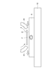
- FIG. 2 is a side view showing an example of the configuration of the temperature stabilizing unit.
- a temperature stabilizing unit 40 as a medium supply unit includes an air tank 41 that contains a gas (medium) such as air, and a regulator (pressure adjusting valve) that adjusts the pressure of the gas released from the air tank 41. ) 42, the air hose 43 that guides the gas G released from the air tank 41 via the regulator 42 to flow along the surface of the integrated circuit S, and the temperature of the surface of the integrated circuit S are detected.
- a temperature controller 44 that controls the regulator 42 so as to be constant.
- the air hose 43 is disposed such that the discharge port is disposed at the end of the surface of the integrated circuit S and faces the center along the surface, and the relative position of the air hose 43 with respect to the integrated circuit S on the sample stage 10 changes. It is fixed with respect to the sample stage 10 so that there is no.
- the temperature control unit 44 includes a temperature detection element (not shown) such as a thermistor disposed in the vicinity of the integrated circuit S, and the regulator 42 so that the temperature value detected by the temperature detection element becomes constant. Is controlled to increase or decrease the pressure of the gas G supplied from the air hose 43.
- FIG. 3 is a plan view showing a gas release state with respect to the integrated circuit S of the temperature stabilization unit 40.
- the air hose 43 of the temperature stabilization unit 40 the size capable of releasing the gas G toward the other end portion S 2 in a range wider than the width of the one end portion S 1 on the surface of the integrated circuit S And has a shape. Accordingly, the temperature stabilization unit 40 can generate a flow along one direction of the gas G with a stable pressure over the entire surface covering the failure portion F of the integrated circuit S. As a result, the temperature stabilization unit 40 can stabilize the temperature of the entire surface of the integrated circuit S at a desired temperature.
- the image processing unit 30 may be configured to be realized by a single control device (for example, a single computer) together with the control unit 20.
- the input device 36 and the display device 37 connected to the image processing unit 30 may function not only as the image processing unit 30 but also as an input device and a display device connected to the control unit 20.
- FIG. 4 is a flowchart showing a procedure of a failure analysis operation related to the integrated circuit S by the integrated circuit failure analysis device 1.
- FIGS. 5 to 9 show signal waveforms processed by the integrated circuit failure analysis device 1 during the failure analysis operation. It is a figure which shows a time change.
- the average temperature of the surface of the integrated circuit S placed on the sample stage 10 is stabilized by operating the temperature stabilization unit 40 (step S01).
- the synchronization controller 23 causes the voltage application unit 14 to lower the frequency of the integrated circuit S.
- Control is performed so as to apply a bias voltage that increases or decreases at (eg, 1 Hz) (step S02).
- a high voltage and a low voltage are periodically applied to the integrated circuit S.
- the imaging device 18 is controlled by the imaging control unit 21 so as to classify and acquire images according to the application timing of the low frequency bias voltage.
- the imaging control unit 21 controls the imaging device 18 so that imaging is performed at the same frequency as the low frequency applied to the integrated circuit S or at an imaging frequency (frame rate) proportional to the low frequency.
- the image of the integrated circuit S acquired in this way is once stored in the image storage unit 31, and then processed by the heat generation signal acquisition unit 32, thereby generating a heat generation detection signal indicating temporal changes in the amount of heat generation at a plurality of points. Is acquired (step S03).
- the synchronization controller 23 controls the voltage application unit 14 to apply a bias voltage that increases or decreases at a high frequency (for example, 2 Hz) from the voltage application unit 14 (step S04). Thereby, a high voltage and a low voltage are periodically applied to the integrated circuit S.
- the imaging device 18 is controlled by the imaging control unit 21 so as to classify and acquire images according to the application timing of the high-frequency bias voltage.
- the imaging control unit 21 controls the imaging device 18 so that imaging is performed at the same frequency as the high frequency applied to the integrated circuit S or at an imaging frequency (frame rate) proportional to the high frequency.
- the image of the integrated circuit S acquired in this way is temporarily stored in the image storage unit 31, and then processed by the heat generation signal acquisition unit 32, thereby acquiring heat generation detection signals at a plurality of points (step S05). ).
- the frequency of the bias voltage applied in steps S02 and S04 may be changed as appropriate. However, if the frequency is too high, the heat transfer and the amount of generated heat will depend on the location. Is preferred. Further, the frequency of the bias voltage to be changed is not limited to two types, but may be changed to three or more types, and the heat generation detection signal may be acquired accordingly.
- FIG. 5 shows the time change of the bias voltage applied in steps S02 and S04.
- the period is controlled by the synchronization control unit 23 so that the high-frequency period P2 follows the low-frequency period P1, and a period for acquiring the heat generation detection signal in each of the period P1 and the period P2.
- a period in which no voltage is applied may be provided between the period P1 and the period P2.
- the maximum voltage V 1 and the minimum voltage V 2 of the bias voltage which are rectangular waves, are set to the same value among a plurality of frequencies so that the conditions during heat generation in the integrated circuit S are equal, and the duty ratio of the bias voltage is also set.
- the same value for example, 50%, 75%, etc. Is set between a plurality of frequencies so that the amount of heat generated in the integrated circuit S is equal. This is to make the average temperature of the sample constant while keeping the amount of heat generated in the integrated circuit S constant. In this case, the period during which the heat generation detection signal is acquired can be continued in each of the period P1 and the period P2.
- phase information of the low-frequency and high-frequency bias voltages applied to the integrated circuit S in steps S02 and 04 is acquired by the voltage phase acquisition unit 33 ( Step S06).
- the heat detection signal corresponding to the application of the low frequency and high frequency bias voltages acquired in steps S03 and S05 is processed, and the phase delay acquisition unit 34 sets the phase of the bias voltage acquired in step S06.
- the phase information based on the information is acquired, and the phase difference between the respective heat generation detection signals is detected (steps S07 and S08).
- the phase difference from the heat generation detection signal is detected for each of the low frequency and high frequency bias voltages.
- the depth information calculation unit 35 calculates the change rate of the phase difference with respect to the square root of the frequency, and the depth information is obtained by multiplying the change rate by a predetermined constant. Calculated (step S09). This depth information is calculated over a plurality of points on the surface of the integrated circuit S. Finally, the calculated depth information is processed as failure analysis information and displayed on the display device 37 (step S10).
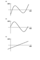
- FIG. 6 shows the time change of the bias voltage applied at a certain frequency, and (b) shows the heat generation detection detected in the integrated circuit S made of a material having a low heat capacity / low heat transfer rate.
- a time change of the signal (c) shows a time change of the heat generation detection signal detected in the integrated circuit S made of a material having a high heat capacity / high heat transfer rate.
- the phase difference calculated by the phase delay acquisition unit 34 of the integrated circuit failure analysis apparatus 1 is D1
- this phase difference D1 includes a phase shift D2 determined by the depth of the heat generation point in the integrated circuit S, and heat generation.
- a phase shift D3 due to differences in heat capacity and heat transfer speed.
- the shift amount D3 greatly depends on the material of the heat transfer path of the integrated circuit S. Further, since the heat transfer coefficient of the integrated circuit S to the air is determined by the surface temperature and convection based on the surface temperature, the shift D3 is greatly influenced by the surface temperature of the integrated circuit S.
- the difference of the phase difference D1 depending on the material can be explained as follows.
- the phase delay per unit, a indicates the attenuation rate per unit length.
- the temperature T with respect to the heat quantity Q is expressed by the following formula (2) as the amount of change when the specific heat is q and the density is ⁇ . Represented by
- the waveform will be distorted. For example, an offset may occur in the phase delay amount.
- the depth of the heat generation source was simply calculated based on this.
- an offset may occur in the actual delay amount. This depends on the heat capacity, the amount of heat generated, the shape, the frequency of the applied bias, etc. in the integrated circuit S.
- the phase offset changes depending on where the integrated circuit S is observed, and it is difficult to always calculate the accurate depth of the heat source.
- the heating detection signal from inside the package of the integrated circuit S changes substantially with respect to the square root of the frequency at a low applied bias frequency with a phase offset of several Hz or less. Take advantage of the lack of.
- the upper limit of the applicable frequency at this time varies depending on the integrated circuit S, but is preferably about 4 Hz or less.
- the depth information detected by the heating point detection method according to the present embodiment is an inclination with respect to the square root of the frequency of the phase delay bx, and the following equation (10): This is the value indicated by. This value depends only on the constants ⁇ , q, ⁇ , and constant ⁇ determined by the physical properties, and the influence of the phase offset can be removed.
- the attenuation rate a is also changed due to the change of the heat transfer coefficient on the surface of the integrated circuit S.
- the heat transfer coefficient from the integrated circuit S to the air varies depending on the surface temperature and convection based on the temperature. Therefore, in order to increase the accuracy of the depth information calculated by the above equation (10), the temperature stabilization unit 40 is provided so that the temperature on the surface of the integrated circuit S is stabilized.
- a temporal change in the temperature of the integrated circuit S can be cited.
- the temperature of the integrated circuit S continues to rise during data acquisition by the image processing unit 30, the slope of the waveform associated with the temperature rise is different from the original phase detection when measuring the phase. Detected as This is shown in FIG.
- the temporal change (FIG. 7 (a)) of the heat generation detection signal detected in the integrated circuit S when the temperature rises on the surface is the integrated circuit when the surface temperature is in a stable state.
- the time change of the heat generation detection signal detected in S (FIG. 7B) is added to the time change of the heat generation detection signal having an inclination corresponding to the temperature rise (FIG. 7C).
- the temperature stabilization unit 40 is also provided to stabilize the surface temperature of the integrated circuit S so that the heat generation detection signal can be acquired in a state where the temporal change of the surface temperature is small.
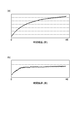
- FIG. 8A shows a time change of the heat generation detection signal acquired by the integrated circuit failure analysis apparatus 1 when the temperature stabilization process by the temperature stabilization unit 40 is not performed
- FIG. These show the time change of the heat generation detection signal acquired by the integrated circuit failure analysis apparatus 1 when the temperature stabilization process by the temperature stabilization unit 40 is performed.
- FIG. 9 shows the time change of the bias voltage applied at a low frequency of 1 Hz
- (b) shows the time change of the heat generation detection signal detected in the integrated circuit S accordingly
- (c) shows the time change of the bias voltage applied at a high frequency of 2 Hz
- (d) shows the time change of the heat generation detection signal detected in the integrated circuit S accordingly.
- the delay corresponding to the phase delay bx is observed as the delay amount D1 at each frequency.
- This delay amount D1 includes a phase shift D2 determined by the depth of the heating point, and a phase shift D3 determined by the sample internal shape, surface state, and the like.
- FIG. 10 shows the relationship between the square root of the angular frequency w of the bias voltage applied to the integrated circuit S and the observed phase delay bx in the integrated circuit failure analysis apparatus 1.
- the phase delay D1 observed at low angular frequency w 1 and the high-angle frequency w 2, respectively, are included a shift amount D2 and the shift amount D3. Therefore, by calculating the slope of the phase delay bx with respect to the square root of the angular frequency w, the phase offset D3 is removed, and the heat capacity and heat generation inside the integrated circuit S determined by the shift D2 determined by the depth of the heat generation point. Depth information independent of position can be estimated.
- a heat generation detection signal corresponding to the application of a low frequency bias voltage is detected from the integrated circuit S, and the high frequency bias voltage is detected.
- a heat generation detection signal corresponding to the application is detected.
- the phase difference between the low frequency bias voltage and the heat generation detection signal and the phase difference between the high frequency bias voltage and the heat generation detection signal are detected. From the rate of change of the phase difference with respect to the square root of the frequency, heat generation is performed. Point depth information is obtained.
- the offset of the temporal change in the heat generation amount that changes depending on the position of the heat generation point is offset and the depth information is calculated, so that highly accurate depth information can be obtained without depending on the position of the heat generation point. Also, by obtaining the rate of change of the phase difference with respect to the variable calculated from the frequency of the bias voltage, it is possible to obtain depth information that does not depend on the amount of heat generated at the heating point, the internal structure of the integrated circuit, and the frequency of the bias voltage. .
- the phase delay bx between the bias voltage and the heat generation detection signal includes deformation of the heat generation detection waveform depending on the amount of heat from the heat generation source, the position of the heat generation point in the integrated circuit S, the internal structure of the integrated circuit, the heat capacity, and the like. Fluctuations are included. Therefore, if the phase delay bx is directly evaluated, the accurate depth of the heating point cannot be calculated. For example, even if a parameter that can calculate an accurate depth at the center of the integrated circuit S is used as it is for a sample edge, a large error occurs.
- Such an error occurs due to a difference in heat transfer speed, a difference in the total heat capacity in the heat transfer range, and a non-linearity of the heat transfer coefficient on the surface of the integrated circuit S.
- the heat capacity changes as shown in FIG. 6 as the heat capacity increases and the speed of heat transfer increases.
- the shift amount D3 accompanying the deformation of the response waveform occurs from 0 degree to 90 degrees at the minimum. This was an extra offset, making it difficult to calculate the correct depth. According to the present embodiment, it is possible to remove such extra offset and obtain accurate depth information.
- the amplitude and duty ratio of the bias voltages of a plurality of frequencies applied to the integrated circuit S are set to be equal to each other, the amount of heat generated at the heat generation point can be made more uniform, and the depth information bias voltage Dependence on the frequency can be further reduced. As a result, more accurate depth information can be acquired.
- the depth information is calculated based on the thermal response to the electric signals having a plurality of frequencies detected after the average temperature of the entire surface of the integrated circuit S is stabilized at a constant temperature.
- Depth information can be obtained stably.
- the infrared radiation intensity increases as the temperature of the integrated circuit S increases. Therefore, by stabilizing the average temperature of the surface of the integrated circuit S at a higher temperature within a range in which the imaging device 18 is not saturated, the temperature of the integrated circuit S is increased. Even if the amplitude is constant, the amplitude of the detection signal can be increased to improve the S / N.
- the waveform of the bias voltage applied to the integrated circuit S is not limited to a rectangular wave, and may be changed to another waveform in which the voltage is periodically increased or decreased, such as a sine wave or a triangular wave.
- the maximum value V 1 and the minimum value V 2 of the bias voltage may be appropriately changed according to the type of the integrated circuit S. However, it is desirable to set the maximum value V 1 and the minimum value V 2 when changing to a plurality of frequencies for one integrated circuit S to be constant.
- the integrated circuit failure analysis apparatus 1 may be provided with a function of automatically detecting and outputting an error when the amplitude of the heat generation detection signal exceeds the measurable range.
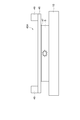
- the temperature stabilization unit 40 that stabilizes the average temperature of the surface of the integrated circuit S may have the following configuration.
- the air hose 43 that has a suction port facing the discharge port of the air hose 43 is added, and the gas is collected by adding an air hose 45 that sucks gas.
- the air hose 43 and the air hose 45 are arranged to oppose each other across the region A 1 on the surface to reliably cover the fault location F ( Figure 12).
- the temperature stabilization unit 40 having such a configuration, the air flow in the region A 1 on the surface of the integrated circuit S constant, can be made uniform the temperature of the entire surface of the integrated circuit S, deep stable Information detection is realized.
- the temperature stabilizing unit 40 is not necessarily limited to supplying a cooled medium (cooling heat medium), and is heated if the surface temperature of the integrated circuit S can be stabilized.
- a medium heat medium for heating
- substrate) 46 is apply
- the high thermal conductive plate 46 disposed close to the integrated circuit S has a size and shape that covers the entire surface of the integrated circuit S, and has a high thermal conductivity such as diamond, Si, SiC, And it is comprised with the material which has a transmittance
- the two cooling elements 48 and 49 are cooling elements such as Peltier elements, and include a temperature detection element (not shown) such as a thermistor arranged near the surface of the integrated circuit S, and are detected by the temperature detection element. Adjust the temperature so that the measured temperature value is constant.
- the cooling elements 48 and 49 may be replaced with a heating element such as a heater element, or may be replaced with a pipe line that circulates the heat medium along the surface of the integrated circuit S. According to the temperature stabilization unit 40A in which the cooling elements 48 and 49 are disposed in the vicinity of the high thermal conductive plate 46, the temperature of the entire surface of the integrated circuit S can be further stabilized.
- a plate-like high heat conduction plate 46 is disposed on the surface of the integrated circuit S with a predetermined gap, and the sample stage 10 and A pair of medium discharge portions 50 and a medium suction portion 51 for supplying a heat medium such as oil in one direction to a gap on the surface of the integrated circuit S are provided at both ends between the high heat conductive plate 46 and the like. It may be a configuration.
- the temperature of the entire surface of the integrated circuit S can be further stabilized by the temperature stabilization unit 40B in which the medium discharge unit 50 and the medium suction unit 51 are disposed in the vicinity of the high thermal conductive plate 46.
- the first phase difference between the periodic electrical signal of the first frequency and the first detection signal, and the periodic electrical signal of the second frequency and the second It is preferable to further include a fifth step of detecting a second phase difference between the detection signal and the detection signal, and in the fourth step, it is preferable to obtain depth information of the heating point based on the first and second phase differences. is there.
- the first phase difference between the periodic electrical signal having the first frequency and the first detection signal, and the periodic electrical signal having the second frequency and the second detection are detected.
- a phase difference detection unit that detects a second phase difference between the signal and the signal is further provided, and the calculation unit obtains depth information of the heat generation point based on the first and second phase differences. is there.
- the offset information of the temporal change in the heat generation amount that changes depending on the position of the heat generation point is offset and the depth information is calculated, so that more accurate depth information can be obtained without depending on the position of the heat generation point. It is done.
- the fourth step between the periodic electrical signal and the detection signal for the variable calculated from the frequency of the periodic electrical signal based on the first and second phase differences. It is also preferable to calculate the change rate of the phase difference and obtain the depth information of the heating point from the change rate. Further, in the above-described heating point detection device, the calculation unit is arranged between the periodic electrical signal and the detection signal with respect to a variable calculated from the frequency of the periodic electrical signal based on the first and second phase differences. It is also preferable to calculate the change rate of the phase difference and obtain the depth information of the heating point from the change rate.
- the temperature stabilization unit has a medium supply unit that supplies a medium so that the average temperature of the surface of the integrated circuit is constant. With such a temperature stabilization unit, the average temperature of the surface of the integrated circuit can be efficiently stabilized with a simple component.
- the temperature stabilization unit has a substrate that is transparent to the infrared region and is disposed close to the integrated circuit, and a temperature adjustment member that is disposed close to the substrate. Is preferred. With this configuration, the average temperature of the entire surface of the integrated circuit can be further stabilized.
- the present invention uses a heat generation point detection method and a heat generation point detection device for detecting the depth of a heat generation point of an integrated circuit, and uses the heat generation point detection device in an integrated circuit to stabilize the depth of the heat generation point accurately and independently of its position. Can be detected.
Landscapes
- General Physics & Mathematics (AREA)
- Physics & Mathematics (AREA)
- Chemical & Material Sciences (AREA)
- General Health & Medical Sciences (AREA)
- Analytical Chemistry (AREA)
- Biochemistry (AREA)
- Life Sciences & Earth Sciences (AREA)
- Health & Medical Sciences (AREA)
- Immunology (AREA)
- Pathology (AREA)
- Engineering & Computer Science (AREA)
- Combustion & Propulsion (AREA)
- Investigating Or Analyzing Materials Using Thermal Means (AREA)
Priority Applications (2)
| Application Number | Priority Date | Filing Date | Title |
|---|---|---|---|
| US14/355,596 US9658116B2 (en) | 2011-11-07 | 2012-08-31 | Method for detecting heat generation points and device for detecting heat generate points |
| KR1020147010865A KR101910697B1 (ko) | 2011-11-07 | 2012-08-31 | 발열점 검출 방법 및 발열점 검출 장치 |
Applications Claiming Priority (2)
| Application Number | Priority Date | Filing Date | Title |
|---|---|---|---|
| JP2011-243891 | 2011-11-07 | ||
| JP2011243891A JP5743855B2 (ja) | 2011-11-07 | 2011-11-07 | 発熱点検出方法及び発熱点検出装置 |
Publications (1)
| Publication Number | Publication Date |
|---|---|
| WO2013069362A1 true WO2013069362A1 (ja) | 2013-05-16 |
Family
ID=48289748
Family Applications (1)
| Application Number | Title | Priority Date | Filing Date |
|---|---|---|---|
| PCT/JP2012/072223 Ceased WO2013069362A1 (ja) | 2011-11-07 | 2012-08-31 | 発熱点検出方法及び発熱点検出装置 |
Country Status (5)
| Country | Link |
|---|---|
| US (1) | US9658116B2 (enExample) |
| JP (1) | JP5743855B2 (enExample) |
| KR (1) | KR101910697B1 (enExample) |
| TW (1) | TWI588479B (enExample) |
| WO (1) | WO2013069362A1 (enExample) |
Cited By (1)
| Publication number | Priority date | Publication date | Assignee | Title |
|---|---|---|---|---|
| JP2022138589A (ja) * | 2021-03-10 | 2022-09-26 | 日本アビオニクス株式会社 | パッケージ品の検査装置およびパッケージ品の検査方法 |
Families Citing this family (6)
| Publication number | Priority date | Publication date | Assignee | Title |
|---|---|---|---|---|
| KR101528200B1 (ko) * | 2014-12-30 | 2015-06-12 | 한국기초과학지원연구원 | 3차원 열영상 측정 장치 및 방법 |
| US10605857B2 (en) * | 2017-05-24 | 2020-03-31 | Rohde & Schwarz Gmbh & Co. Kg | Anechoic chamber for testing a device under test |
| CN113466253A (zh) * | 2020-03-31 | 2021-10-01 | 苏州阿特斯阳光电力科技有限公司 | 太阳能电池热斑缺陷的检测方法与检测设备 |
| US11243550B2 (en) | 2020-05-29 | 2022-02-08 | Juniper Networks, Inc. | Optical-electrical device using hybrid automated testing equipment |
| CN114264933B (zh) * | 2021-12-21 | 2024-02-13 | 厦门宇昊软件有限公司 | 一种集成电路板的故障检测方法和故障检测系统 |
| CN118566704B (zh) * | 2024-06-21 | 2025-01-10 | 广东金鉴实验室科技有限公司 | 一种显微红外热点定位测试机 |
Citations (6)
| Publication number | Priority date | Publication date | Assignee | Title |
|---|---|---|---|---|
| JPH06207914A (ja) * | 1993-01-11 | 1994-07-26 | Hitachi Ltd | 欠陥検出方法と装置および赤外線検出方法と装置 |
| JPH06265496A (ja) * | 1993-01-13 | 1994-09-22 | Kobe Steel Ltd | 試料の欠陥評価方法 |
| JPH11337511A (ja) * | 1998-05-25 | 1999-12-10 | Advantest Corp | 回路検査装置および方法 |
| JP2003035690A (ja) * | 2001-07-24 | 2003-02-07 | Taiyo Yuden Co Ltd | 検査方法及び検査装置 |
| JP2005291791A (ja) * | 2004-03-31 | 2005-10-20 | Takahide Sakagami | コンクリートの充填不良検査方法および装置 |
| JP2007024674A (ja) * | 2005-07-15 | 2007-02-01 | Hitachi Ltd | 表面・表層検査装置、及び表面・表層検査方法 |
Family Cites Families (8)
| Publication number | Priority date | Publication date | Assignee | Title |
|---|---|---|---|---|
| DE19837889C1 (de) * | 1998-08-20 | 2000-12-21 | Siemens Ag | Thermowellen-Meßverfahren |
| US7401976B1 (en) * | 2000-08-25 | 2008-07-22 | Art Advanced Research Technologies Inc. | Detection of defects by thermographic analysis |
| JP4097079B2 (ja) * | 2004-02-27 | 2008-06-04 | ▲隆▼英 阪上 | 欠陥検査方法およびその装置 |
| US7394659B2 (en) * | 2004-11-19 | 2008-07-01 | International Business Machines Corporation | Apparatus and methods for cooling semiconductor integrated circuit package structures |
| TW200801487A (en) | 2006-06-23 | 2008-01-01 | Innolux Display Corp | Method and device for detecting circuit |
| KR101260146B1 (ko) | 2008-09-17 | 2013-05-02 | 신닛테츠스미킨 카부시키카이샤 | 재료의 표면 상의 그리고 표면 층 내의 결함의 양쪽 모두를 검출하는 방법 그리고 이러한 방법을 위한 시스템 |
| KR101716104B1 (ko) * | 2010-06-08 | 2017-03-14 | 디씨지 시스템스 인코포레이티드 | 3-차원 핫 스팟 위치추정 |
| EP2444795A1 (en) | 2010-10-22 | 2012-04-25 | DCG Systems, Inc. | Lock in thermal laser stimulation through one side of the device while acquiring lock-in thermal emission images on the opposite side |
-
2011
- 2011-11-07 JP JP2011243891A patent/JP5743855B2/ja active Active
-
2012
- 2012-08-31 KR KR1020147010865A patent/KR101910697B1/ko active Active
- 2012-08-31 US US14/355,596 patent/US9658116B2/en active Active
- 2012-08-31 WO PCT/JP2012/072223 patent/WO2013069362A1/ja not_active Ceased
- 2012-11-01 TW TW101140594A patent/TWI588479B/zh active
Patent Citations (6)
| Publication number | Priority date | Publication date | Assignee | Title |
|---|---|---|---|---|
| JPH06207914A (ja) * | 1993-01-11 | 1994-07-26 | Hitachi Ltd | 欠陥検出方法と装置および赤外線検出方法と装置 |
| JPH06265496A (ja) * | 1993-01-13 | 1994-09-22 | Kobe Steel Ltd | 試料の欠陥評価方法 |
| JPH11337511A (ja) * | 1998-05-25 | 1999-12-10 | Advantest Corp | 回路検査装置および方法 |
| JP2003035690A (ja) * | 2001-07-24 | 2003-02-07 | Taiyo Yuden Co Ltd | 検査方法及び検査装置 |
| JP2005291791A (ja) * | 2004-03-31 | 2005-10-20 | Takahide Sakagami | コンクリートの充填不良検査方法および装置 |
| JP2007024674A (ja) * | 2005-07-15 | 2007-02-01 | Hitachi Ltd | 表面・表層検査装置、及び表面・表層検査方法 |
Cited By (2)
| Publication number | Priority date | Publication date | Assignee | Title |
|---|---|---|---|---|
| JP2022138589A (ja) * | 2021-03-10 | 2022-09-26 | 日本アビオニクス株式会社 | パッケージ品の検査装置およびパッケージ品の検査方法 |
| JP7624655B2 (ja) | 2021-03-10 | 2025-01-31 | 日本アビオニクス株式会社 | パッケージ品の検査装置およびパッケージ品の検査方法 |
Also Published As
| Publication number | Publication date |
|---|---|
| TWI588479B (zh) | 2017-06-21 |
| KR20140075757A (ko) | 2014-06-19 |
| TW201329441A (zh) | 2013-07-16 |
| US20140294038A1 (en) | 2014-10-02 |
| US9658116B2 (en) | 2017-05-23 |
| JP2013101005A (ja) | 2013-05-23 |
| JP5743855B2 (ja) | 2015-07-01 |
| KR101910697B1 (ko) | 2018-10-22 |
Similar Documents
| Publication | Publication Date | Title |
|---|---|---|
| JP5743855B2 (ja) | 発熱点検出方法及び発熱点検出装置 | |
| JP5745629B2 (ja) | 発熱点検出方法及び発熱点検出装置 | |
| TWI491868B (zh) | 量測熱擴散係數的裝置以及量測熱擴散係數的方法 | |
| CN101527274A (zh) | 基板表面温度测量方法、基板处理设备、半导体器件制造方法 | |
| US20210109047A1 (en) | Method and device for measuring transverse thermal conductivity of thin film | |
| Ansari Hosseinzadeh et al. | Finite amplitude effects on drop levitation for material properties measurement | |
| CN107843616A (zh) | 快速测量薄膜材料的热导率的装置和方法 | |
| Song et al. | Experimental investigation of evaporation-induced convection in water using laser based measurement techniques | |
| Gong et al. | An experimental study of rupture dynamics of evaporating liquid films on different heater surfaces | |
| US10641694B2 (en) | Measuring interfacial tension using electrostatic oscillations | |
| JP2024527544A (ja) | レーザーダイオード装置、レーザーダイオードの動作方法及びレーザーダイオードを備えた走査型顕微鏡装置 | |
| JP4658366B2 (ja) | 熱物性測定方法 | |
| JP4258667B2 (ja) | 熱物性測定方法及び装置 | |
| Straube et al. | Estimation of heat loss in thermal wave experiments | |
| WO2016056109A1 (ja) | 解析装置及び解析方法 | |
| JP3607234B2 (ja) | 熱伝導率推定方法および熱伝導率推定装置 | |
| Kabaši et al. | Automated 3-omega thermal conductivity measurement system by dynamically balanced Wheatstone bridge | |
| JP2010025724A (ja) | 温度測定装置,温度測定方法 | |
| JP3937018B2 (ja) | 薄膜の膜厚及び密度の測定方法並びに測定装置 | |
| JP2019138869A (ja) | 熱物性測定方法 | |
| Ceja-Morales et al. | Optimizing thermal diffusivity measurements for fluids with accessible 3D printing and Arduino-based temperature control | |
| Aloian et al. | Piezoelectric Resonance Laser Calorimetry for Determination of Low Optical Absorption Coefficients of Polyhedron Crystal Boules | |
| JP2010238864A (ja) | 半導体デバイス製造工程の汚染評価方法 | |
| Karaoğlu et al. | A study on Marangoni convection by the variational iteration method | |
| JP2013217675A (ja) | 力学物性測定装置及び力学物性測定方法 |
Legal Events
| Date | Code | Title | Description |
|---|---|---|---|
| 121 | Ep: the epo has been informed by wipo that ep was designated in this application |
Ref document number: 12847624 Country of ref document: EP Kind code of ref document: A1 |
|
| ENP | Entry into the national phase |
Ref document number: 20147010865 Country of ref document: KR Kind code of ref document: A |
|
| WWE | Wipo information: entry into national phase |
Ref document number: 14355596 Country of ref document: US |
|
| NENP | Non-entry into the national phase |
Ref country code: DE |
|
| 122 | Ep: pct application non-entry in european phase |
Ref document number: 12847624 Country of ref document: EP Kind code of ref document: A1 |