WO2013062041A1 - 導電性フイルム及びタッチパネル - Google Patents
導電性フイルム及びタッチパネル Download PDFInfo
- Publication number
- WO2013062041A1 WO2013062041A1 PCT/JP2012/077589 JP2012077589W WO2013062041A1 WO 2013062041 A1 WO2013062041 A1 WO 2013062041A1 JP 2012077589 W JP2012077589 W JP 2012077589W WO 2013062041 A1 WO2013062041 A1 WO 2013062041A1
- Authority
- WO
- WIPO (PCT)
- Prior art keywords
- conductive
- spiral
- conductive film
- pattern
- connection
- Prior art date
- Legal status (The legal status is an assumption and is not a legal conclusion. Google has not performed a legal analysis and makes no representation as to the accuracy of the status listed.)
- Ceased
Links
Images




Classifications
-
- G—PHYSICS
- G06—COMPUTING OR CALCULATING; COUNTING
- G06F—ELECTRIC DIGITAL DATA PROCESSING
- G06F3/00—Input arrangements for transferring data to be processed into a form capable of being handled by the computer; Output arrangements for transferring data from processing unit to output unit, e.g. interface arrangements
- G06F3/01—Input arrangements or combined input and output arrangements for interaction between user and computer
- G06F3/03—Arrangements for converting the position or the displacement of a member into a coded form
- G06F3/041—Digitisers, e.g. for touch screens or touch pads, characterised by the transducing means
- G06F3/044—Digitisers, e.g. for touch screens or touch pads, characterised by the transducing means by capacitive means
- G06F3/0445—Digitisers, e.g. for touch screens or touch pads, characterised by the transducing means by capacitive means using two or more layers of sensing electrodes, e.g. using two layers of electrodes separated by a dielectric layer
-
- G—PHYSICS
- G06—COMPUTING OR CALCULATING; COUNTING
- G06F—ELECTRIC DIGITAL DATA PROCESSING
- G06F1/00—Details not covered by groups G06F3/00 - G06F13/00 and G06F21/00
- G06F1/16—Constructional details or arrangements
- G06F1/1613—Constructional details or arrangements for portable computers
- G06F1/1633—Constructional details or arrangements of portable computers not specific to the type of enclosures covered by groups G06F1/1615 - G06F1/1626
- G06F1/1684—Constructional details or arrangements related to integrated I/O peripherals not covered by groups G06F1/1635 - G06F1/1675
- G06F1/169—Constructional details or arrangements related to integrated I/O peripherals not covered by groups G06F1/1635 - G06F1/1675 the I/O peripheral being an integrated pointing device, e.g. trackball in the palm rest area, mini-joystick integrated between keyboard keys, touch pads or touch stripes
- G06F1/1692—Constructional details or arrangements related to integrated I/O peripherals not covered by groups G06F1/1635 - G06F1/1675 the I/O peripheral being an integrated pointing device, e.g. trackball in the palm rest area, mini-joystick integrated between keyboard keys, touch pads or touch stripes the I/O peripheral being a secondary touch screen used as control interface, e.g. virtual buttons or sliders
-
- G—PHYSICS
- G06—COMPUTING OR CALCULATING; COUNTING
- G06F—ELECTRIC DIGITAL DATA PROCESSING
- G06F3/00—Input arrangements for transferring data to be processed into a form capable of being handled by the computer; Output arrangements for transferring data from processing unit to output unit, e.g. interface arrangements
- G06F3/01—Input arrangements or combined input and output arrangements for interaction between user and computer
- G06F3/03—Arrangements for converting the position or the displacement of a member into a coded form
- G06F3/041—Digitisers, e.g. for touch screens or touch pads, characterised by the transducing means
- G06F3/044—Digitisers, e.g. for touch screens or touch pads, characterised by the transducing means by capacitive means
- G06F3/0446—Digitisers, e.g. for touch screens or touch pads, characterised by the transducing means by capacitive means using a grid-like structure of electrodes in at least two directions, e.g. using row and column electrodes
-
- H—ELECTRICITY
- H05—ELECTRIC TECHNIQUES NOT OTHERWISE PROVIDED FOR
- H05K—PRINTED CIRCUITS; CASINGS OR CONSTRUCTIONAL DETAILS OF ELECTRIC APPARATUS; MANUFACTURE OF ASSEMBLAGES OF ELECTRICAL COMPONENTS
- H05K1/00—Printed circuits
- H05K1/02—Details
-
- G—PHYSICS
- G06—COMPUTING OR CALCULATING; COUNTING
- G06F—ELECTRIC DIGITAL DATA PROCESSING
- G06F2203/00—Indexing scheme relating to G06F3/00 - G06F3/048
- G06F2203/041—Indexing scheme relating to G06F3/041 - G06F3/045
- G06F2203/04111—Cross over in capacitive digitiser, i.e. details of structures for connecting electrodes of the sensing pattern where the connections cross each other, e.g. bridge structures comprising an insulating layer, or vias through substrate
-
- G—PHYSICS
- G06—COMPUTING OR CALCULATING; COUNTING
- G06F—ELECTRIC DIGITAL DATA PROCESSING
- G06F2203/00—Indexing scheme relating to G06F3/00 - G06F3/048
- G06F2203/041—Indexing scheme relating to G06F3/041 - G06F3/045
- G06F2203/04112—Electrode mesh in capacitive digitiser: electrode for touch sensing is formed of a mesh of very fine, normally metallic, interconnected lines that are almost invisible to see. This provides a quite large but transparent electrode surface, without need for ITO or similar transparent conductive material
Definitions
- the present invention relates to a conductive film and a touch panel provided with the conductive film.
- Touch panels are mainly applied to small sizes such as PDAs (personal digital assistants) and mobile phones, but are expected to increase in size due to application to personal computer displays.
- the conductive film according to US Patent Application Publication No. 2004/0239650 and US Pat. No. 7,202,859 is formed by arranging a pattern in which a plurality of S-shaped deformed portions are formed in each metal wire in the vertical direction.
- 1 conductive pattern and a 2nd conductive pattern comprised by arranging the pattern in which the some S-shaped deformation
- the first conductive pattern and the second conductive pattern are arranged so that the deformed portions intersect each other. Also in this case, the intersection of each thin metal wire of the first conductive pattern and each thin metal wire of the second conductive pattern and its vicinity function as a cell for accumulating charges.
- the boundary between the ladder pattern of the first conductive pattern and the ladder pattern of the second conductive pattern is easily visible, so that visibility is improved. There is also a problem in terms of (the property that the conductive pattern is not visually recognized by the naked eye).
- the present invention has been made in consideration of such problems, has good translucency and visibility, can improve the output dynamic range with respect to input, and improve the sensitivity and detection of touch position detection.
- An object is to provide a conductive film and a touch panel capable of improving accuracy.
- a conductive film according to a first aspect of the present invention includes a base and a conductive portion formed on one main surface of the base, and the conductive portion includes a plurality of pad portions each having a connection portion.
- Each of the pad portions includes a first spiral portion extending from one connection portion, a second spiral portion extending from the other connection portion, and the first spiral portion.
- a connecting portion that connects the spiral portion and the second spiral portion, wherein the first spiral portion and the second spiral portion are each configured by combining a plurality of lattices, and the connecting portion includes a plurality of conductive wires. It is comprised by these.
- each of the peripheral edges of the first spiral part and the second spiral part has an uneven shape with a peak or a valley at the top of the lattice.
- the plurality of conducting wires constituting the connecting portion are each formed in a linear shape.
- a dummy pattern is formed between the conductive patterns by a fine metal wire that is not connected to the conductive pattern.
- the dummy pattern is arranged between a connection part in one of the conductive patterns and a connection part in the other conductive pattern.
- each periphery of the first spiral part and the second spiral part has at least one long side part and two or more long side parts in which one side of the lattice is continuously arranged linearly. And an overhanging portion formed by a thin metal wire extending orthogonally from the side portion.
- the conductive film according to the second aspect of the present invention includes a base, a first conductive portion formed on one main surface of the base, and a second conductive portion formed on the other main surface of the base.
- the first conductive part has two or more first conductive patterns formed of thin metal wires each having a plurality of first pad parts connected via a first connection part, and the first conductive part is
- the plurality of second pad portions each have two or more second conductive patterns formed of thin metal wires connected via the second connection portions, and each of the first pad portions extends from one first connection portion.
- a second connecting portion that connects the third spiral portion and the fourth spiral portion, and the first spiral portion to the fourth spiral portion are each configured by combining a plurality of lattices,
- One connecting part and the second connecting part are constituted by a plurality of conductive wires, and the first conductive pattern and the second conductive pattern are arranged so that the first connecting part and the second connecting part are substantially orthogonal to each other. It is characterized by being.
- each of the peripheral edges of the first spiral portion to the fourth spiral portion has a concavo-convex shape having a peak or a valley as a vertex of the lattice.
- the first conductive pattern and the second conductive pattern are such that the second connecting portion is located between the adjacent first conductive patterns, and between the adjacent second conductive patterns. It arrange
- the first conductive pattern and the second conductive pattern are located between the first spiral portion and the second spiral portion in the first conductive pattern.
- the third spiral part or the fourth spiral part is located in the second conductive pattern, and the first spiral part or the fourth spiral part in the first conductive pattern is between the third spiral part and the fourth spiral part in the second conductive pattern. It arrange
- a first dummy pattern is formed between the first conductive patterns by a fine metal wire that is not connected to the first conductive pattern.
- a second dummy pattern is formed by a thin metal wire that is not connected to the two conductive patterns.
- the first dummy pattern is disposed between the first connection portion in one of the first conductive patterns and the first connection portion in the other first conductive pattern.
- the second dummy pattern is disposed between the second connection portion in one of the second conductive patterns and the second connection portion in the other second conductive pattern.
- the second connection portion is located between the first dummy patterns, and the first connection is between the second dummy patterns.
- the parts are arranged so as to be positioned.
- the number of the lattices constituting the first spiral portion and the second spiral portion of the first conductive pattern is the third spiral portion and the fourth spiral of the second conductive pattern. Fewer than the number of the lattices constituting the spiral portion.
- each of the peripheral edges of the first spiral portion and the second spiral portion has at least one of two or more first long side portions in which one side of the lattice is continuously arranged linearly.
- Each of the third spiral portion and the fourth spiral portion is linearly continuous with one side of the lattice. It has two or more 2nd long side parts located in a line, and the 2nd overhang
- the first long side portion where the first overhang portion is formed and the second long side portion where the second overhang portion is not formed are opposed to each other. It is characterized by.
- the first long side portion where the first overhang portion is not formed and the second long side portion where the second overhang portion is formed are opposed to each other. It is characterized by.
- the length of one side of each of the lattices is 100 to 400 ⁇ m.
- the line width of each of the lattices is 1 to 15 ⁇ m.
- a touch panel is a touch panel including a conductive film installed on a display panel of a display device, and the conductive film is formed on a substrate and one main surface of the substrate.
- a conductive portion formed, and the conductive portion has two or more conductive patterns formed of thin metal wires each having a plurality of pad portions connected via connection portions, and each of the pad portions is connected to one side.
- a touch panel is a touch panel including a conductive film installed on a display panel of a display device, and the conductive film is formed on a base and one main surface of the base.
- a first conductive portion formed; and a second conductive portion formed on the other main surface of the base.
- the first conductive portion includes a plurality of first pad portions via the first connection portion.
- Two or more first conductive patterns formed of thin metal wires connected to each other, and the first conductive portion includes two or more first conductive patterns formed of metal thin wires each having a plurality of second pad portions connected via the second connection portions.
- Each of the first pad portions includes a first spiral portion extending from one first connection portion, a second spiral portion extending from the other first connection portion, the first spiral portion, and the first spiral portion.
- a first connecting part for connecting the second spiral part, and each front The second pad portion connects the third spiral portion extending from one second connection portion, the fourth spiral portion extending from the other second connection portion, and the third spiral portion and the fourth spiral portion.
- Each of the first spiral portion to the fourth spiral portion is configured by combining a plurality of lattices, and the first connection portion and the second connection portion are configured by a plurality of conductive wires.
- the first conductive pattern and the second conductive pattern are arranged such that the first connection portion and the second connection portion are substantially orthogonal to each other.
- the transparency and visibility are good, the output dynamic range for input can be improved, and the sensitivity of touch position detection is improved.
- the detection accuracy can be improved.
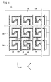
- FIG. 1 is a plan view in which a part of the pattern of the first conductive portion of the conductive film (first conductive film) according to the first embodiment is omitted.
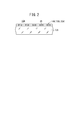
- FIG. 2 is a cross-sectional view showing the first conductive film with a part thereof omitted.
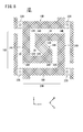
- FIG. 3 is an enlarged plan view showing the first pad portion, the first connection portion, and the first dummy pattern of the first conductive film.
- FIG. 4 is an exploded perspective view showing a configuration of a touch panel having a laminated conductive film.
- FIG. 5 is an exploded perspective view in which a part of the laminated conductive film is omitted.
- FIG. 6A is a cross-sectional view showing an example of a laminated conductive film with a part thereof omitted.
- FIG. 6B is a cross-sectional view illustrating another example of the laminated conductive film with a part omitted.
- FIG. 7 is a plan view showing a partially omitted pattern of the second conductive portion of the conductive film (second conductive film) according to the second embodiment.
- FIG. 8 is an enlarged plan view showing the second pad portion, the second connection portion, and the second dummy pattern of the second conductive film.
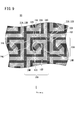
- FIG. 9 is a plan view showing a partially omitted example in which a laminated conductive film is formed by combining the first conductive film and the second conductive film.
- FIG. 10 is a flowchart showing a method for manufacturing a conductive film according to the present embodiment.
- FIG. 10 is a flowchart showing a method for manufacturing a conductive film according to the present embodiment.
- FIG. 11A is a cross-sectional view in which a part of the produced photosensitive material is omitted.
- FIG. 11B is an explanatory diagram showing double-sided simultaneous exposure on a photosensitive material.
- the first exposure process and the second exposure are performed so that the light irradiated to the first photosensitive layer does not reach the second photosensitive layer, and the light irradiated to the second photosensitive layer does not reach the first photosensitive layer. It is explanatory drawing which shows the state which is performing the exposure process.
- ⁇ indicating a numerical range is used as a meaning including numerical values described before and after the numerical value as a lower limit value and an upper limit value.
- the conductive film according to the first embodiment (hereinafter referred to as the first conductive film 10A) is formed on one main surface of the first transparent substrate 12A (see FIG. 2).
- the first conductive portion 14A is provided.
- the first conductive portion 14A is disposed between two or more first conductive patterns 20A and a first conductive pattern 20A, each of which is formed by a thin metal wire in which a plurality of first pad portions 16A are connected via a first connection portion 18A.
- the first conductive pattern 20A and the first dummy pattern 22A made of a thin metal wire that is not connected to the first conductive pattern 20A.
- the fine metal wire is made of, for example, gold (Au), silver (Ag), or copper (Cu).
- One first conductive pattern 20A is configured by arranging two or more first pad portions 16A in the x direction (first direction) via the first connection portions 18A, respectively. Two or more first conductive patterns 20A are arranged in the y direction (second direction) orthogonal to the x direction.
- the x direction indicates the horizontal direction (or vertical direction) of a projection capacitive touch panel 100 (see FIG. 4), which will be described later, or the horizontal direction (or vertical direction) of the display panel 110 on which the touch panel 100 is installed.
- Each first pad portion 16A includes a first spiral portion 24A extending from one first connection portion 18A, a second spiral portion 24B extending from the other first connection portion 18A, a first spiral portion 24A, and a second spiral portion. And a first connecting portion 26A that connects 24B.
- the first spiral portion 24A, the second spiral portion 24B, and the first connection portion 18A are each configured by combining a plurality of lattices 28. 26 A of 1st connection parts are comprised by the some conducting wire 30.
- the lattice 28 has the smallest square shape or rhombus shape.
- the length of one side of the first pad portion 16A is preferably 3 to 10 mm, and more preferably 4 to 6 mm. If the length of one side is less than the above lower limit value, when the first conductive film 10A is used for a touch panel, for example, the capacitance of the first pad portion 16A at the time of detection is reduced, so that detection failure may occur. Increases nature. On the other hand, if the upper limit is exceeded, the position detection accuracy may be reduced. From the same viewpoint, the length of one side of the lattice 28 constituting the first pad portion 16A is preferably 100 to 400 ⁇ m, more preferably 150 to 300 ⁇ m, and most preferably 210 to 250 ⁇ m or less. .
- the transparency (translucency) can be further kept good, and the display can be visually recognized without discomfort when attached to the front surface of the display device. be able to.
- the line width of the lattice 28, that is, the line width of the fine metal wire is 1 to 15 ⁇ m. Thereby, combined with the length of one side of the lattice 28, the conductivity and transparency (translucency) are improved.
- Each peripheral edge of the first spiral portion 24A and the second spiral portion 24B has an uneven shape with the peak of the lattice 28 being a mountain or a valley.
- the first spiral portion 24A includes a plurality of combinations in which three lattices 28 are arranged in the fourth direction (n-direction) (a combination in which the sides are adjacent to each other) from one first connection portion 18A to the other first connection portion 18A.
- a plurality of the above combinations are arranged along the second direction from the bent portion of the first spiral portion 24A.
- eight lattices 28 are arranged in the fourth direction along the side, and the six lattices are sequentially arranged in the second direction.
- the lattices 28 are arranged in such a manner that the lattices 28 are reduced by two, such as a lattice, four lattices, and two lattices.
- the second spiral portion 24B there are a plurality of combinations in which the three lattices 28 are arranged in the fourth direction (n direction) from the other first connection portion 18A toward the one first connection portion 18A.
- a plurality of the above combinations are arranged along the second direction from the bent portion of the second spiral portion 24B.
- eight lattices 28 are arranged in the fourth direction along the side, and the six lattices are sequentially arranged in the second direction.
- the gratings 28 are arranged in such a manner that the gratings 28 are reduced by two, such as four gratings and two gratings.
- the above description shows how to arrange the lattices 28 mainly in the fourth direction, and may be described in a form mainly in the third direction or a form in which the third direction and the fourth direction are combined. Of course you can.
- each of the peripheral edges of the first spiral portion 24A and the second spiral portion 24B has at least one first long side portion 32A and two or more first long side portions 32A in which one side of the lattice 28 is continuously arranged linearly.
- the first long side part 32A is formed at the inner peripheral edge of the bent part, and the outer peripheral edge of the bent part and the metal at each end edge.
- a first projecting portion 34A is formed by a thin line.
- the first connecting portion 26A is constituted by, for example, four linear conducting wires 30 extending in the third direction.
- the length of each conductive wire 30 is eight times the length of one side of the lattice 28 in the examples of FIGS. 1 and 3, but depends on the distance between the first spiral portion 24A and the second spiral portion 24B. However, it may be an integral multiple of the length of one side of the lattice 28.
- the extending direction of the conducting wire 30 is not limited to the third direction, and includes the first direction, the second direction, the fourth direction, and the like according to the positions of the terminal end of the first spiral part 24A and the terminal end of the second spiral part 24B. It is done.
- the first dummy pattern 22A is disposed between two adjacent first conductive patterns 20A, and in particular, the first connection portion 18A of one first conductive pattern 20A and the first connection portion 18A of the other first conductive pattern 20A. It is arranged between.
- the first connecting portions 18 ⁇ / b> A are connected by a plurality of gratings 28 (for example, a combination in which three gratings 28 are arranged in the third direction or the fourth direction are arranged in the second direction. ) From which a part of the fine metal wires are removed, for example, a shape in which the fine metal wires at the boundary with the first connecting portion 18A and the fine metal wires at the center are removed.
- each first conductive pattern 20A is an open end.
- the end portion of the first pad portion 16A existing on the other end portion side of each first conductive pattern 20A is electrically connected to the first terminal wiring pattern 38A made of a thin metal wire via the first connection portion 36A (see FIG. 4), for example. Connected.
- one first conductive pattern 20A is configured by arranging two or more first pad portions 16A in the x direction via the first connection portions 18A.
- One pad portion 16A includes a first spiral portion 24A extending from one first connection portion 18A, a second spiral portion 24B extending from the other first connection portion 18A, a first spiral portion 24A, and a second spiral portion 24B.
- the first spiral portion 24A and the second spiral portion 24B are each configured by combining a plurality of lattices 28, and the first link portion 26A is formed by a plurality of conductors 30. Since it was comprised, it becomes possible to reduce electric resistance significantly rather than the structure which forms one electrode with one ITO film
- the response speed can be increased and the touch panel can be increased in size.
- the first spiral portion 24A, the second spiral portion 24B, and the first connection portion 18A are each in a form in which a large number of lattices 28 are arranged, even if a disconnection occurs locally in the thin metal wire, Conduction is ensured by the thin wire, and the influence of disconnection can be avoided.
- the number of signal charges accumulated in one first pad portion 16A is increased by the large number of gratings 28, and as a result, the output dynamic range with respect to the input is increased.
- the sensitivity (detection sensitivity) for detecting the touch position of the fingertip can be increased, and the signal component with respect to the noise component is increased.
- the S / N ratio can be improved. This leads to an improvement in touch position detection accuracy.
- the touch panel 100 includes a sensor main body 102 and a control circuit (configured by an IC circuit or the like) not shown.
- the sensor body 102 is a laminated body according to the present embodiment, which is constructed by laminating the first conductive film 10A and the second conductive film 10B described later. It has a conductive film 50 and a protective layer 106 laminated thereon (the description of the protective layer 106 is omitted in FIG. 6A).
- the laminated conductive film 50 and the protective layer 106 are arranged on the display panel 110 in the display device 108 such as a liquid crystal display.
- the sensor main body 102 When viewed from above, the sensor main body 102 has a sensor unit 112 disposed in a region corresponding to the display screen 110 a of the display panel 110 and a terminal wiring unit 114 disposed in a region corresponding to the outer peripheral portion of the display panel 110. (So-called picture frame).
- the first conductive film 10 ⁇ / b> A applied to the touch panel 100 has a large number of the first conductive patterns 20 ⁇ / b> A described above arranged in portions corresponding to the sensor portions 112.
- a plurality of first terminal wiring patterns 38A are arranged by fine metal wires led out from one connection portion 36A.
- the outer shape of the first conductive film 10A has a rectangular shape when viewed from above, and the outer shape of the sensor unit 112 also has a rectangular shape.
- a peripheral portion on one long side of the first conductive film 10A has a plurality of first terminals 116A in the length direction of the one long side at a central portion in the length direction.
- An array is formed.
- a plurality of first connection parts 36A are arranged in a straight line along one long side of sensor part 112 (long side closest to one long side of first conductive film 10A: y direction).
- the first terminal wiring pattern 38A derived from each first connection portion 36A is routed toward a substantially central portion on one long side of the first conductive film 10A, and is electrically connected to the corresponding first terminal 116A. It is connected to the. Accordingly, the first terminal wiring patterns 38A connected to the first connection portions 36A corresponding to both sides of one long side in the sensor unit 112 are routed with substantially the same length.
- the first terminal 116A may be formed at or near the corner of the first conductive film 10A, but the longest first terminal wiring pattern 38A and the shortest first terminal wiring pattern 38A among the plurality of first terminal wiring patterns 38A.
- a large difference in length occurs between the one-terminal wiring pattern 38A and signal transmission to the first conductive pattern 20A corresponding to the longest first terminal-wiring pattern 38A and a plurality of first terminal-wiring patterns 38A in the vicinity thereof.
- the first terminal 116A is formed at the central portion in the length direction of one long side of the first conductive film 10A, thereby suppressing local signal transmission delay. Can do. This leads to an increase in response speed.
- the second conductive film 10B has a second conductive portion 14B formed on one main surface of the second transparent substrate 12B.
- the second conductive portion 14B is disposed between the second conductive patterns 20B and the two or more second conductive patterns 20B formed of metal thin wires in which a plurality of second pad portions 16B are connected via the second connection portions 18B, respectively.
- the second conductive pattern 20B and the second dummy pattern 22B made of a thin metal wire that is not connected to the second conductive pattern 20B.
- One second conductive pattern 20B is configured by arranging two or more second pad portions 16B in the y direction (second direction) via the second connection portions 18B. Two or more second conductive patterns 20B are arranged in the x direction (first direction).
- Each second pad portion 16B includes a third spiral portion 24C extending from one second connection portion 18B, a fourth spiral portion 24D extending from the other second connection portion 18B, a third spiral portion 24C, and a fourth spiral portion. And a second connecting portion 26B that connects 24D.
- the third spiral portion 24C, the fourth spiral portion 24D, and the second connection portion 18B are each configured by combining a plurality of lattices 28.
- the second connecting portion 26 ⁇ / b> B is composed of a plurality of conducting wires 30.
- the length of one side of the second pad portion 16B is preferably 3 to 10 mm, and more preferably 4 to 6 mm.
- the length of one side of the grating 28 constituting the second pad portion 16B is preferably 100 to 400 ⁇ m, more preferably 150 to 300 ⁇ m, and most preferably 210 to 250 ⁇ m or less.
- the line width of the lattice 28, that is, the line width of the fine metal wire is 1 to 15 ⁇ m.
- the peripheral edges of the third spiral portion 24 ⁇ / b> C and the fourth spiral portion 24 ⁇ / b> D have an uneven shape in which the apexes of the lattice 28 are peaks or valleys, respectively.
- the lattices satisfying this form there are various ways of arranging the lattices satisfying this form, and one form of arrangement is as follows. That is, in the third spiral portion 24C, a plurality of combinations in which five lattices 28 are arranged in the third direction (m direction) are arranged from one second connection portion 18B to the other second connection portion 18B, A plurality of the above combinations are arranged along the first direction (x direction) from the bent portion of the spiral portion 24C.
- 11 lattices 28 are arranged in the third direction along the side, and 10 lattices 28 are adjacent to the lattice.
- the lattices 28 are reduced by two in order toward the first direction. It is arranged.
- the fourth spiral portion 24D there are a plurality of combinations in which five lattices 28 are arranged in the third direction (m direction) from the other second connection portion 18B to the one second connection portion 18B.
- a plurality of the above combinations are arranged along the first direction from the bent portion of the fourth spiral portion 24D.
- 11 lattices 28 are arranged in the third direction along the side, and 10 lattices 28 are adjacent to the second lattice portion 26D.
- the gratings 28 are arranged in three directions, and are sequentially arranged in the first direction, with eight gratings, six gratings, four gratings, and two gratings. ing. Further, the number of the lattices 28 constituting the second pad portion 16B is larger than the number of the lattices 28 constituting the first pad portion 16A.
- the above description shows how to arrange the lattices 28 mainly in the third direction, and may be described in a form mainly based on the fourth direction or a form in which the third direction and the fourth direction are combined. Of course you can.
- each of the peripheral edges of the third spiral portion 24C and the fourth spiral portion 24D has two or more second long side portions 32B in which one side of the lattice 28 is continuously and linearly arranged, and at least one second long side portion 32B. And a second overhanging portion 34B made of a thin metal wire extending orthogonally from the second portion 34B.
- the second long side part 32B is formed on the inner peripheral edge of the bent part, and the second thin metal wire is formed on the outer peripheral edge of the bent part.
- An overhang portion 34B is formed.
- the 2nd connection part 26B is comprised by the six linear conducting wires 30 extended in the 4th direction, for example.
- the length of each conducting wire 30 is four times the length of one side of the grating 28 in the examples of FIGS. 7 and 8, but depends on the separation length between the third spiral portion 24C and the fourth spiral portion 24D. However, it may be an integral multiple of the length of one side of the lattice 28.
- the extending direction of the conducting wire 30 is not limited to the fourth direction, and the first direction, the second direction, the third direction, etc., depending on the positions of the terminal edge of the third spiral part 24C and the terminal edge of the fourth spiral part 24D. Is mentioned.
- the second dummy pattern 22B is disposed between two adjacent second conductive patterns 20B, and in particular, the second connection portion 18B of one second conductive pattern 20B and the second connection portion 18B of the other second conductive pattern 20B. It is arranged between.
- the second connecting portions 18 ⁇ / b> B are connected by a plurality of lattices 28 (for example, a combination in which three lattices 28 are arranged in the first direction and the second direction (a combination in which vertices are adjacently arranged)).
- a shape obtained by removing a part of the fine metal wires for example, a shape obtained by removing the fine metal wires at the boundary portion of the second connecting portion 18B and the fine metal wires between the lattice 28 at the central portion and the peripheral edge portion of the combination described above.
- the second dummy pattern 22B has one lattice 28 disposed in the center portion and a plurality of wavy shapes that are disposed so as to sandwich the lattice 28 and the sides of the lattice are arranged.
- every other (for example, odd-numbered) second conductive pattern 20B and one other end of the even-numbered second conductive pattern 20B are open ends.
- the second pad portion 16B existing on the other end portion side of each odd-numbered second conductive pattern 20B and the second end portion existing on one end portion side of each even-numbered second conductive pattern 20B.
- the end portions of the pad portions 16B are electrically connected to the second terminal wiring patterns 38B made of fine metal wires through the second connection portions 36B.
- a large number of second conductive patterns 20B are arranged in a portion corresponding to the sensor unit 112, and a plurality of second terminal wiring patterns 38B derived from the second connection parts 36B are arranged in the terminal wiring unit 114. Yes.
- a plurality of second terminals 116 ⁇ / b> B are provided at the peripheral portion on one long side of the second conductive film 10 ⁇ / b> B in the center portion in the longitudinal direction.
- the long side is arranged in the length direction.
- a plurality of second connection portions 36B (for example, odd-numbered second connection portions) along one short side of the sensor portion 112 (short side closest to one short side of the second conductive film 10B: x direction).
- second connection portions 36B are arranged in a straight line, and a plurality of second connection portions 36B (for example, along the other short side of the sensor unit 112 (the short side closest to the other short side of the second conductive film 10B: the x direction))
- the even-numbered second connection portions 36B are arranged linearly.
- odd-numbered second conductive patterns 20B are connected to the corresponding odd-numbered second connection portions 36B, respectively, and even-numbered second conductive patterns 20B are respectively corresponding even-numbered. It is connected to the second second connection part 36B.
- the second terminal wiring pattern 38B derived from the odd-numbered second connection part 36B and the second terminal wiring pattern 38B derived from the even-numbered second connection part 36B are one long side of the second conductive film 10B. And are electrically connected to the corresponding second terminals 116B. Accordingly, for example, the first and second terminal wiring patterns 38B are routed with substantially the same length.
- the second terminal 116B may be formed at or near the corner of the second conductive film 10B, but as described above, the longest second terminal wiring pattern 38B and a plurality of second terminal wirings in the vicinity thereof. There is a problem that signal transmission to the second conductive pattern 20B corresponding to the pattern 38B is delayed. Therefore, as in this embodiment, the second terminal 116B is formed in the central portion in the length direction of one long side of the second conductive film 10B, thereby suppressing local signal transmission delay. Can do. This leads to an increase in response speed.
- the first terminal wiring pattern 38A may be derived in the same manner as the second terminal wiring pattern 38B, and the second terminal wiring pattern 38B may be derived in the same manner as the first terminal wiring pattern 38A.
- a protective layer is formed on the first conductive film 10A and the first conductive pattern 20A derived from the multiple first conductive patterns 20A of the first conductive film 10A.
- the terminal wiring pattern 38A and the second terminal wiring pattern 38B derived from the many second conductive patterns 20B of the second conductive film 10B are connected to, for example, a control circuit that controls scanning.
- a self-capacitance method or a mutual capacitance method can be preferably employed. That is, in the case of the self-capacitance method, voltage signals for touch position detection are sequentially supplied to the first conductive pattern 20A, and voltage signals for touch position detection are sequentially supplied to the second conductive pattern 20B. Supply. Since the capacitance between the first conductive pattern 20A and the second conductive pattern 20B facing the touch position and GND (ground) is increased by bringing the fingertip into contact with or close to the upper surface of the protective layer 106, the first conductive pattern The waveforms of the transmission signals from 20A and the second conductive pattern 20B are different from the waveforms of the transmission signals from the other conductive patterns.
- the control circuit calculates the touch position based on the transmission signal supplied from the first conductive pattern 20A and the second conductive pattern 20B.
- a voltage signal for touch position detection is sequentially supplied to the first conductive pattern 20A, and sensing (detection of a transmission signal) is sequentially performed on the second conductive pattern 20B.
- sensing detection of a transmission signal
- the stray capacitance of the finger is added in parallel to the parasitic capacitance between the first conductive pattern 20A and the second conductive pattern 20B facing the touch position.
- the waveform of the transmission signal from the second conductive pattern 20B is different from the waveform of the transmission signal from the other second conductive pattern 20B. Therefore, in the control circuit, the touch position is calculated based on the order of the first conductive pattern 20A that supplies the voltage signal and the transmission signal from the supplied second conductive pattern 20B.
- the first conductive pattern 20A and the second conductive pattern 20B are arranged as shown in FIG. It becomes a state.
- the line widths of the first conductive pattern 20A and the second conductive pattern 20B are the same, in FIG. 9, the first conductive pattern 20A is shown so that the positions of the first conductive pattern 20A and the second conductive pattern 20B can be seen.
- the line width of the second conductive pattern 20B is exaggerated and made thin.
- the first connecting part 26A (see FIG. 1) of the first conductive pattern 20A and the second connecting part 26B (see FIG. 7) of the second conductive pattern 20B are arranged so as to be substantially orthogonal to each other, and the first connecting part
- the combination part 120 of 26A and the 2nd connection part 26B becomes a form with which the some grating
- the second connection portion 18B of the second conductive pattern 20B is positioned between the adjacent first conductive patterns 20A, and the first connection portion 18A of the first conductive pattern 20A is positioned between the adjacent second conductive patterns 20B.
- the lattices 28 are arranged. The same applies to the boundary between the second conductive pattern 20B and the first connection portion 18A.
- the third spiral portion 24C or the fourth spiral portion 24D in the second conductive pattern 20B is located between the first spiral portion 24A and the second spiral portion 24B in the first conductive pattern 20A, and the second conductive pattern Between the third spiral portion 24C and the fourth spiral portion 24D in 20B, the first spiral portion 24A or the second spiral portion 24B in the first conductive pattern 20A is disposed.
- the apexes overlap, and the projection distance between the sides of the grid 28 is substantially equal to the length of one side of the grid 28, so that a plurality of grids 28 are arranged.
- the second connection portion 18B is located between the first dummy patterns 22A in the first direction (x direction), and the first connection portion 18A is located between the second dummy patterns 22B in the second direction (y direction).
- the vertices of the lattices 28 overlap each other, and the projection distance between the sides of the lattice 28 is substantially equal to the length of one side of the lattice 28.
- the lattices 28 are arranged. The same applies to the boundary between the second dummy pattern 22B and the first connection portion 18A.
- the first long side portion 32A in which the first overhang portion 34A is formed and the second long side portion 32B in which the second overhang portion 34B is not formed face each other, and the first overhang portion 34A is formed.
- the first long side portion 32A that is not present and the second long side portion 32B on which the second projecting portion 34B is formed are arranged to face each other, and a plurality of lattices 28 are arranged.
- the first dummy pattern 22A and the second dummy pattern 22B are opposed to each other, and the portion of the first dummy pattern 22A from which the fine metal wires are removed is supplemented by the fine metal wires of the second dummy pattern 22B.
- the portion from which the fine metal wires are removed is arranged so that the fine metal wires of the first dummy pattern 22A supplement, and a plurality of lattices 28 are arranged.
- each of the first spiral portion 24A to the fourth spiral portion 24D is formed as a straight line portion in which the sides of the lattice 28 are arranged in a straight line without having an uneven shape with the apexes of the lattice 28 as peaks or valleys.
- the linear portion of the first spiral portion 24A and the linear portion of the third spiral portion 24C or the fourth spiral portion 24D are overlapped, and the linear portion of the second spiral portion 24B and the third spiral portion 24C or the fourth spiral portion 24D.
- each of the peripheral edges of the first spiral portion 24A to the fourth spiral portion 24D has an uneven shape with the apexes of the lattice 28 as peaks or valleys.
- the boundary between 16A and the second pad portion 16B becomes inconspicuous, and visibility is improved.
- the third spiral portion is directly below the straight portion of the first spiral portion 24A.
- the straight portion of 24C or the fourth spiral portion 24D is located, and the straight portion of the third spiral portion 24C or the fourth spiral portion 24D is located immediately below the straight portion of the second spiral portion 24B.
- the linear part of the second spiral part 24B is between the linear part of the first spiral part 24A and the linear part of the third spiral part 24C or the fourth spiral part 24D.
- Parasitic capacitance is formed between the first spiral portion 24C and the straight portion of the fourth spiral portion 24C or the fourth spiral portion 24D, and the presence of this parasitic capacitance acts as a noise component on the charge information, causing a significant decrease in the S / N ratio.
- a parasitic capacitance is formed between each first pad portion 16A and each second pad portion 16B, a large number of parasitic capacitances are connected in parallel to the first conductive pattern 20A and the second conductive pattern 20B. As a result, there is a problem that the CR time constant becomes large.
- the rise time of the waveform of the voltage signal supplied to the first conductive pattern 20A (and the second conductive pattern 20B) is delayed, and an electric field for position detection is hardly generated in a predetermined scan time. There is a risk that it will not be performed.
- the rise time or fall time of the waveform of the transmission signal from the first conductive pattern 20A and the second conductive pattern 20B is also delayed, and there is a possibility that the change in the waveform of the transmission signal cannot be captured during a predetermined scan time. . This leads to a decrease in detection accuracy and a decrease in response speed.
- first pad portions 16A and second pad portions 16B must be reduced (reduction in resolution) or the size of the display screen to be adapted must be reduced. For example, there arises a problem that it cannot be applied to B5 version, A4 version, and larger screens.
- each peripheral edge of the first spiral portion 24A to the fourth spiral portion 24D has an uneven shape with the peaks of the lattice 28 as peaks or valleys.
- the vertices of the lattices 28 overlap, and the lattice 28
- the projection distance Lf (see FIG. 6A) between the sides 28a is substantially equal to the length of one side of the lattice 28.
- each of the plurality of first overhang portions 34A in the first pad portion 16A is opposed to the corresponding second long side portion 32B of the second pad portion 16B, and the plurality of second overhang portions in the second pad portion 16B. Since each of the portions 34B only faces the corresponding first long side portion 32A of the first pad portion 16A, the parasitic capacitance formed between the first pad portion 16A and the second pad portion 16B is small. Become. As a result, the CR time constant is also reduced, and the detection accuracy and response speed can be improved.
- the optimum distance of the projection distance Lf described above is not the size of the first pad portion 16A and the second pad portion 16B, but the size of the lattice 28 (line width and one side) constituting the first pad portion 16A and the second pad portion 16B. It is preferable to set appropriately according to the length. In this case, if the size of the grating 28 is too large with respect to the first pad portion 16A and the second pad portion 16B having a certain size, the translucency is improved, but the dynamic range of the transmission signal is reduced. There is a risk of causing a decrease in detection sensitivity. On the other hand, if the size of the grating 28 is too small, the detection sensitivity is improved, but there is a limit to the reduction of the line width, so that the translucency may be deteriorated.
- the optimum value (optimum distance) of the projection distance Lf is preferably 100 to 400 ⁇ m, more preferably 200 to 300 ⁇ m, when the line width of the grating 28 is 1 to 15 ⁇ m. If the line width of the grating 28 is narrowed, the above-mentioned optimum distance can be shortened. However, since the electric resistance increases, the CR time constant increases even if the parasitic capacitance is small. There is a risk of lowering the response speed. Therefore, the line width of the grating 28 is preferably in the above range.
- a plurality of first terminals 116A are formed in the central portion in the longitudinal direction at the peripheral edge of one long side of the first conductive film 10A in the terminal wiring portion 114, and the second conductive film is formed.
- a plurality of second terminals 116 ⁇ / b> B are formed in the central portion in the length direction of the peripheral portion on one long side of 10 ⁇ / b> B.
- the first terminal 116A and the second terminal 116B are arranged so as not to overlap with each other, and further, the first terminal wiring pattern 38A and the second terminal wiring pattern 38B are arranged. To avoid overlapping.
- the first terminal 116A and, for example, the odd-numbered second terminal wiring pattern 38B may partially overlap each other.
- the plurality of first terminals 116A and the plurality of second terminals 116B are connected to two connectors (first terminal connector and second terminal connector) or one connector (first terminal 116A and second terminal 116B). And can be electrically connected to the control circuit via a cable.
- first terminal wiring pattern 38A and the second terminal wiring pattern 38B are not overlapped with each other, generation of parasitic capacitance between the first terminal wiring pattern 38A and the second terminal wiring pattern 38B is suppressed. , A decrease in response speed can be suppressed.
- the area of the terminal wiring part 114 can be reduced. This can promote downsizing of the display panel 110 including the touch panel 100, and can make the display screen 110a look impressively large. In addition, the operability as the touch panel 100 can be improved.
- the distance between the adjacent first terminal wiring patterns 38A and the distance between the adjacent second terminal wiring patterns 38B is preferably 10 ⁇ m to 50 ⁇ m.
- the distance between the adjacent first terminal wiring patterns 38A be 50 ⁇ m or more and 100 ⁇ m or less.
- the response speed can be increased, and the large size of the touch panel 100 can be achieved. Can be promoted.
- the boundary between the first pad portion 16A of the first conductive film 10A and the second pad portion 16B of the second conductive film 10B becomes inconspicuous, and the first connecting portion 26A and the second connecting portion 26B are combined.
- the plurality of gratings 28 are formed by the combination of the first dummy pattern 22A and the second dummy pattern 22B, there is no inconvenience such as local line thickening, and the visibility is improved as a whole.
- first conductive patterns 20A and second conductive patterns 20B can be significantly reduced, thereby increasing the response speed and detecting the position within the drive time (scan time). Will also be easier. This leads to an increase in the screen size of the touch panel 100 (vertical x horizontal size, not including thickness).
- the distance from the finger touch position is increased. Even in the second pad portion 16B, which is far from the first pad portion 16B, it is possible to accumulate signal charges equivalent to those in the first pad portion 16A, and the detection sensitivity in the first conductive film 10A and the detection in the second conductive film 10B. Sensitivity can be made substantially equal, the burden of signal processing can be reduced, and detection accuracy can be improved.
- the signal charge accumulated in the second pad portion 16B having a large number of lattices 28 is read out, so that the output dynamic range with respect to the input can be increased, and the S of the detection signal can be increased.
- the / N ratio can be improved, the detection sensitivity can be improved, and the detection accuracy can be improved.
- the first conductive portion 14A is formed on one main surface of the first transparent substrate 12A, and the second conductive substrate 50B is formed on the second main surface.
- the conductive portion 14B is formed, as shown in FIG. 6B, the first conductive portion 14A is formed on one main surface of the first transparent base 12A, and the first main surface 14A is formed on the other main surface.
- the two conductive portions 14B may be formed.
- the second transparent substrate 12B does not exist, the first transparent substrate 12A is laminated on the second conductive portion 14B, and the first conductive portion 14A is laminated on the first transparent substrate 12A.
- the first conductive film 10A and the second conductive film 10B may have other layers between them, and if the first conductive part 14A and the second conductive part 14B are in an insulated state, they are You may arrange
- the first alignment mark 118a and the second alignment mark 118b are preferably formed.
- the first alignment mark 118a and the second alignment mark 118b become a new composite alignment mark when the first conductive film 10A and the second conductive film 10B are bonded to form a laminated conductive film 50.
- the alignment mark also functions as an alignment mark for positioning used when the laminated conductive film 50 is installed on the display panel 110.
- the first conductive film 10A and the second conductive film 10B are applied to the projected capacitive touch panel 100.
- a surface capacitive touch panel, a resistor, It can also be applied to a membrane touch panel.
- the first conductive film 10A is laminated on the second conductive film 10B to form the laminated conductive film 50.
- the second conductive film 10B is formed on the first conductive film 10A.
- the laminated conductive film 50 may be formed by laminating.
- the number of the lattices 28 constituting the first pad portion 16A and the number of the lattices 28 constituting the second pad portion 16B may be the same.
- first overhanging portion 34A on the first pad portion 16A may be omitted, and the second overhanging portion 34B may be formed on each of the second long side portions 32B of the second pad portion 16B.
- the formation of the second projecting portion 34B on the second pad portion 16B may be omitted, and the first projecting portion 34A may be formed on each first long side portion 32A of the first pad portion 16A.
- the first conductive pattern 20A and the second conductive pattern 20B for example, a photosensitive having an emulsion layer containing a photosensitive silver halide salt on the first transparent substrate 12A and the second transparent substrate 12B.
- the first conductive pattern 20A and the second conductive pattern 20B may be formed by exposing the material and performing development processing to form a metallic silver portion and a light transmissive portion in the exposed portion and the unexposed portion, respectively. Good. In addition, you may make it carry
- the first conductive pattern 20A is formed on one main surface of the first transparent substrate 12A and the second conductive pattern 20B is formed on the other main surface of the first transparent substrate 12A
- the method of exposing one principal surface first and then exposing the other principal surface in accordance with the manufacturing method is employed, the desired first conductive pattern 20A and second conductive pattern 20B may not be obtained.
- the following production method can be preferably employed.
- the photosensitive silver halide emulsion layer formed on both surfaces of the first transparent substrate 12A is collectively exposed to form the first conductive pattern 20A on one main surface of the first transparent substrate 12A.
- the second conductive pattern 20B is formed on the other main surface of the transparent substrate 12A.
- a long photosensitive material 140 is prepared.
- the photosensitive material 140 includes a first transparent substrate 12A and a photosensitive silver halide emulsion layer (hereinafter referred to as a first photosensitive layer 142a) formed on one main surface of the first transparent substrate 12A. And a photosensitive silver halide emulsion layer (hereinafter referred to as a second photosensitive layer 142b) formed on the other main surface of the first transparent substrate 12A.
- step S2 of FIG. 10 the photosensitive material 140 is exposed.
- the first photosensitive layer 142a is irradiated with light toward the first transparent substrate 12A to expose the first photosensitive layer 142a along the first exposure pattern, and the second photosensitive layer.
- the layer 142b is subjected to a second exposure process in which light is irradiated toward the first transparent substrate 12A to expose the second photosensitive layer 142b along the second exposure pattern (double-sided simultaneous exposure).
- double-sided simultaneous exposure double-sided simultaneous exposure
- the first photosensitive layer 142a is irradiated with the first light 144a (parallel light) through the first photomask 146a and the second photosensitive material 140a is irradiated.
- the layer 142b is irradiated with the second light 144b (parallel light) through the second photomask 146b.
- the first light 144a is obtained by converting the light emitted from the first light source 148a into parallel light by the first collimator lens 150a
- the second light 144b is emitted from the second light source 148b. It is obtained by converting the light into parallel light by the second collimator lens 150b in the middle.
- first light source 148a and second light source 148b the case where two light sources (first light source 148a and second light source 148b) are used is shown, but the light emitted from one light source is divided through the optical system to generate the first light.
- the first photosensitive layer 142a and the second photosensitive layer 142b may be irradiated as the 144a and the second light 144b.
- the exposed photosensitive material 140 is developed to produce a laminated conductive film 50 as shown in FIG. 6B.
- the laminated conductive film 50 includes a first transparent substrate 12A, a first conductive portion 14A (first conductive pattern 20A, etc.) along a first exposure pattern formed on one main surface of the first transparent substrate 12A. And a second conductive portion 14B (second conductive pattern 20B, etc.) along the second exposure pattern formed on the other main surface of the first transparent substrate 12A.
- the exposure time and development time of the first photosensitive layer 142a and the second photosensitive layer 142b vary depending on the type of the first light source 148a and the second light source 148b, the type of the developer, and the like. However, the exposure time and the development time are adjusted so that the development rate becomes 100%.
- a first photomask 146a is closely disposed on the first photosensitive layer 142a, for example, and the first photomask 146a.
- the first photosensitive layer 142a is exposed by irradiating the first light 144a from the first light source 148a disposed opposite to the first photomask 146a.
- the first photomask 146a includes a glass substrate made of transparent soda glass and a mask pattern (first exposure pattern 152a) formed on the glass substrate. Therefore, the first exposure process exposes a portion of the first photosensitive layer 142a along the first exposure pattern 152a formed on the first photomask 146a.
- a gap of about 2 to 10 ⁇ m may be provided between the first photosensitive layer 142a and the first photomask 146a.
- the second photomask 146b is disposed in close contact with the second photosensitive layer 142b, and the second photomask 146b from the second light source 148b disposed to face the second photomask 146b.
- the second photosensitive layer 142b is exposed by irradiating the second light 144b toward.
- the second photomask 146b includes a glass substrate formed of transparent soda glass and a mask pattern (second exposure pattern 152b) formed on the glass substrate. Yes.
- the second exposure process exposes a portion of the second photosensitive layer 142b along the second exposure pattern 152b formed on the second photomask 146b. In this case, a gap of about 2 to 10 ⁇ m may be provided between the second photosensitive layer 142b and the second photomask 146b.
- the emission timing of the first light 144a from the first light source 148a and the emission timing of the second light 144b from the second light source 148b may be made simultaneously or differently. Also good.
- the first photosensitive layer 142a and the second photosensitive layer 142b can be exposed simultaneously by one exposure process, and the processing time can be shortened.
- both the first photosensitive layer 142a and the second photosensitive layer 142b are not spectrally sensitized, when the photosensitive material 140 is exposed from both sides, the exposure from one side affects the image formation on the other side (back side). Will be affected.
- the first light 144a from the first light source 148a that has reached the first photosensitive layer 142a is scattered by the silver halide grains in the first photosensitive layer 142a, passes through the first transparent substrate 12A as scattered light, Part of it reaches the second photosensitive layer 142b. Then, the boundary portion between the second photosensitive layer 142b and the first transparent substrate 12A is exposed over a wide range, and a latent image is formed. For this reason, in the second photosensitive layer 142b, the exposure with the second light 144b from the second light source 148b and the exposure with the first light 144a from the first light source 148a are performed, and in the subsequent development processing, the laminated conductive film is formed.
- a thin conductive layer by the first light 144a from the first light source 148a is formed between the conductive patterns, A desired pattern (pattern along the second exposure pattern 152b) cannot be obtained.
- the thickness of the first photosensitive layer 142a and the second photosensitive layer 142b is set to a specific range, and the amount of silver applied to the first photosensitive layer 142a and the second photosensitive layer 142b is specified. By doing so, it was found that the silver halide itself absorbs light and can limit light transmission to the back surface.
- the thickness of the first photosensitive layer 142a and the second photosensitive layer 142b can be set to 1 ⁇ m or more and 4 ⁇ m or less. The upper limit is preferably 2.5 ⁇ m.
- the coating silver amount of the first photosensitive layer 142a and the second photosensitive layer 142b was regulated to 5 to 20 g / m 2 .
- the silver halide with a reduced amount of binder provided the necessary conductivity for antistatic, and the volume ratio of silver / binder in the first photosensitive layer 142a and the second photosensitive layer 142b was defined. . That is, the silver / binder volume ratio of the first photosensitive layer 142a and the second photosensitive layer 142b is 1/1 or more, and preferably 2/1 or more.
- the first photosensitive layer 142a can be formed as shown in FIG.
- the reached first light 144a from the first light source 148a does not reach the second photosensitive layer 142b.
- the second light 144b from the second light source 148b that reaches the second photosensitive layer 142b is changed to the first photosensitive layer.
- one main surface of the first transparent substrate 12A is electrically conductive by the first exposure pattern 152a.
- the first photosensitive layer 142a and the second photosensitive layer 142b that have both conductivity and suitability for double-sided exposure.
- the same pattern or different patterns can be arbitrarily formed on both surfaces of the first transparent substrate 12A, whereby the electrodes of the touch panel 100 can be easily formed,
- the touch panel 100 can be thinned (low profile).
- the above example is a manufacturing method in which the first conductive pattern 20A and the second conductive pattern 20B are formed using a photosensitive silver halide emulsion layer.
- Other manufacturing methods include the following manufacturing methods. .
- the photoresist film on the copper foil formed on the first transparent substrate 12A and the second transparent substrate 12B is exposed and developed to form a resist pattern, and the copper foil exposed from the resist pattern is etched.
- the first conductive pattern 20A and the second conductive pattern 20B may be formed.
- the first conductive pattern 20A and the second conductive pattern 20B are formed by printing a paste containing metal fine particles on the first transparent substrate 12A and the second transparent substrate 12B and performing metal plating on the paste. Also good.
- the first conductive pattern 20A and the second conductive pattern 20B may be printed and formed on the first transparent substrate 12A and the second transparent substrate 12B by a screen printing plate or a gravure printing plate.
- the first conductive pattern 20A and the second conductive pattern 20B may be formed by inkjet on the first transparent base 12A and the second transparent base 12B.
- the manufacturing method of the first conductive film 10A and the second conductive film 10B according to the present embodiment includes the following three modes depending on the photosensitive material and the type of development processing.
- a photosensitive silver halide black-and-white photosensitive material that does not contain physical development nuclei and an image-receiving sheet having a non-photosensitive layer that contains physical development nuclei are overlapped and transferred to develop a non-photosensitive image-receiving sheet. Form formed on top.
- the above aspect (1) is an integrated black-and-white development type, and a light-transmitting conductive film such as a light-transmitting conductive film is formed on the photosensitive material.
- the resulting developed silver is chemically developed silver or heat developed silver, and is highly active in the subsequent plating or physical development process in that it is a filament with a high specific surface.
- the light-transmitting conductive film such as a light-transmitting conductive film is formed on the photosensitive material by dissolving silver halide grains close to the physical development nucleus and depositing on the development nucleus in the exposed portion.
- a characteristic film is formed.
- This is also an integrated black-and-white development type. Although the development action is precipitation on the physical development nuclei, it is highly active, but developed silver is a sphere with a small specific surface.
- the silver halide grains are dissolved and diffused in the unexposed area and deposited on the development nuclei on the image receiving sheet, whereby a light transmitting conductive film or the like is formed on the image receiving sheet.
- a conductive film is formed. This is a so-called separate type in which the image receiving sheet is peeled off from the photosensitive material.
- either negative development processing or reversal development processing can be selected (in the case of the diffusion transfer method, negative development processing is possible by using an auto-positive type photosensitive material as the photosensitive material).
- first transparent substrate 12A and the second transparent substrate 12B examples include a plastic film, a plastic plate, and a glass plate.
- polyesters such as polyethylene terephthalate (PET) and polyethylene naphthalate (PEN); polyolefins such as polyethylene (PE), polypropylene (PP), polystyrene, and EVA; Resin;
- polycarbonate (PC) polyamide, polyimide, acrylic resin, triacetyl cellulose (TAC) and the like can be used.
- PET melting point: 258 ° C.
- PEN melting point: 269 ° C.
- PE melting point: 135 ° C.
- PP melting point: 163 ° C.
- polystyrene melting point: 230 ° C.
- polyvinyl chloride melting point: 180 ° C.
- polyvinylidene chloride melting point: 212 ° C.
- TAC melting point: 290 ° C.
- PET is preferable from the viewpoints of light transmittance and processability.
- the conductive films such as the first conductive film 10A and the second conductive film 10B used in the laminated conductive film 50 are required to be transparent, the transparency of the first transparent substrate 12A and the second transparent substrate 12B is required. Is preferably high.
- the conductive layers of the first conductive film 10A and the second conductive film 10B (conductive portions such as the first pad portion 16A, the first connection portion 18A, the second pad portion 16B, the second connection portion 18B, and the lattice 28) are formed.
- the silver salt emulsion layer contains additives such as a solvent and a dye in addition to the silver salt and the binder.
- Examples of the silver salt used in the present embodiment include inorganic silver salts such as silver halide and organic silver salts such as silver acetate. In the present embodiment, it is preferable to use silver halide having excellent characteristics as an optical sensor.
- Silver coating amount of silver salt emulsion layer is preferably 1 ⁇ 30g / m 2 in terms of silver, more preferably 1 ⁇ 25g / m 2, more preferably 5 ⁇ 20g / m 2 .
- coating amount of silver salt is preferably 1 ⁇ 30g / m 2 in terms of silver, more preferably 1 ⁇ 25g / m 2, more preferably 5 ⁇ 20g / m 2 .
- binder used in this embodiment examples include gelatin, polyvinyl alcohol (PVA), polyvinyl pyrrolidone (PVP), starch and other polysaccharides, cellulose and derivatives thereof, polyethylene oxide, polyvinyl amine, chitosan, polylysine, and polyacryl.
- PVA polyvinyl alcohol
- PVP polyvinyl pyrrolidone
- starch and other polysaccharides, cellulose and derivatives thereof, polyethylene oxide, polyvinyl amine, chitosan, polylysine, and polyacryl.
- acid polyalginic acid, polyhyaluronic acid, carboxycellulose and the like. These have neutral, anionic, and cationic properties depending on the ionicity of the functional group.
- the content of the binder contained in the silver salt emulsion layer of the present embodiment is not particularly limited and can be appropriately determined as long as dispersibility and adhesion can be exhibited.
- the binder content in the silver salt emulsion layer is preferably 1 ⁇ 4 or more, more preferably 1 ⁇ 2 or more in terms of the silver / binder volume ratio.
- the silver / binder volume ratio is preferably 100/1 or less, and more preferably 50/1 or less.
- the silver / binder volume ratio is more preferably 1/1 to 4/1. Most preferably, it is 1/1 to 3/1.
- the silver / binder volume ratio is converted from the amount of silver halide / binder amount (weight ratio) of the raw material to the amount of silver / binder amount (weight ratio), and the amount of silver / binder amount (weight ratio) is further converted to the amount of silver. / It can obtain
- the solvent used for forming the silver salt emulsion layer is not particularly limited.
- water organic solvents (for example, alcohols such as methanol, ketones such as acetone, amides such as formamide, dimethyl sulfoxide, etc. Sulphoxides such as, esters such as ethyl acetate, ethers, etc.), ionic liquids, and mixed solvents thereof.
- the content of the solvent used in the silver salt emulsion layer of the present embodiment is in the range of 30 to 90% by mass with respect to the total mass of silver salt and binder contained in the silver salt emulsion layer, and 50 to 80%. It is preferably in the range of mass%.
- a protective layer (not shown) may be provided on the silver salt emulsion layer.
- the “protective layer” means a layer made of a binder such as gelatin or a high molecular polymer, and is provided on a silver salt emulsion layer having photosensitivity in order to exhibit the effect of preventing scratches and improving mechanical properties. It is formed.
- the thickness is preferably 0.5 ⁇ m or less.
- the coating method and forming method of the protective layer are not particularly limited, and a known coating method and forming method can be appropriately selected.
- An undercoat layer for example, can be provided below the silver salt emulsion layer.
- the present embodiment includes the case where the first conductive pattern 20A and the second conductive pattern 20B are applied by a printing method, but the first conductive pattern 20A and the second conductive pattern 20B are formed by exposure and development, etc., except for the printing method.
- exposure is performed on a photosensitive material having a silver salt-containing layer provided on the first transparent substrate 12A and the second transparent substrate 12B or a photosensitive material coated with a photolithography photopolymer.
- the exposure can be performed using electromagnetic waves. Examples of the electromagnetic wave include light such as visible light and ultraviolet light, and radiation such as X-rays.
- a light source having a wavelength distribution may be used for exposure, or a light source having a specific wavelength may be used.
- development processing is further performed.
- the development processing can be performed by a normal development processing technique used for silver salt photographic film, photographic paper, printing plate-making film, photomask emulsion mask, and the like.
- the developer is not particularly limited, but PQ developer, MQ developer, MAA developer and the like can also be used.
- Commercially available products include, for example, CN-16, CR-56, CP45X, FD prescribed by FUJIFILM Corporation. -3, Papitol, developers such as C-41, E-6, RA-4, D-19, and D-72 prescribed by KODAK, or developers included in the kit can be used.
- a lith developer can also be used.
- the development processing in the present invention can include a fixing processing performed for the purpose of removing and stabilizing the silver salt in an unexposed portion.
- a fixing process technique used for silver salt photographic film, photographic paper, film for printing plate making, emulsion mask for photomask, and the like can be used.
- the fixing temperature in the fixing step is preferably about 20 ° C. to about 50 ° C., more preferably 25 ° C. to 45 ° C.
- the fixing time is preferably 5 seconds to 1 minute, more preferably 7 seconds to 50 seconds.
- the replenishing amount of the fixing solution is preferably 600 ml / m 2 or less with respect to the processing of the photosensitive material, more preferably 500 ml / m 2 or less, 300 ml / m 2 or less is particularly preferred.
- the light-sensitive material that has been subjected to development and fixing processing is preferably subjected to water washing treatment or stabilization treatment.
- the washing water amount is usually 20 liters or less per 1 m 2 of the light-sensitive material, and can be replenished in 3 liters or less (including 0, ie, rinsing with water).
- the mass of the metallic silver contained in the exposed portion after the development treatment is preferably a content of 50% by mass or more, and 80% by mass or more with respect to the mass of silver contained in the exposed portion before exposure. More preferably. If the mass of silver contained in the exposed portion is 50% by mass or more based on the mass of silver contained in the exposed portion before exposure, it is preferable because high conductivity can be obtained.
- the gradation after the development processing in the present embodiment is not particularly limited, but is preferably more than 4.0.
- the conductivity of the conductive metal portion can be increased while keeping the light transmissive property of the light transmissive portion high.
- means for setting the gradation to 4.0 or higher include the aforementioned doping of rhodium ions and iridium ions.
- the conductive film is obtained through the above steps, but the surface resistance of the obtained conductive film is 0.1 to 100 ohm / sq. It is preferable that it exists in the range.
- the lower limit is 1 ohm / sq. Is preferably 10 ohm / sq. More preferably.
- the upper limit is 70 ohm / sq. And preferably 50 ohm / sq. More preferably.
- the conductive film after the development treatment may be further subjected to a calendar treatment, and can be adjusted to a desired surface resistance by the calendar treatment.
- the conductive metal particles may be supported on the metallic silver portion by only one of physical development and plating treatment, or the conductive metal particles are supported on the metallic silver portion by combining physical development and plating treatment. Also good.
- the thing which performed the physical development and / or the plating process to the metal silver part is called "conductive metal part".
- “physical development” means that metal ions such as silver ions are reduced with a reducing agent on metal or metal compound nuclei to deposit metal particles. This physical phenomenon is used for instant B & W film, instant slide film, printing plate manufacturing, and the like, and the technology can be used in the present invention.
- the physical development may be performed simultaneously with the development processing after exposure or separately after the development processing.
- the plating treatment can be performed using electroless plating (chemical reduction plating or displacement plating), electrolytic plating, or both electroless plating and electrolytic plating.
- electroless plating chemical reduction plating or displacement plating
- electrolytic plating electrolytic plating
- electrolytic plating electrolytic plating
- electroless plating in the present embodiment a known electroless plating technique can be used, for example, an electroless plating technique used in a printed wiring board or the like can be used. Plating is preferred.
- Oxidation treatment it is preferable to subject the metallic silver portion after the development treatment and the conductive metal portion formed by physical development and / or plating treatment to oxidation treatment.
- oxidation treatment for example, when a metal is slightly deposited on the light transmissive portion, the metal can be removed and the light transmissive portion can be made almost 100% transparent.
- the lower limit of the line width of the conductive metal portion of this embodiment is preferably 1 ⁇ m or more, 3 ⁇ m or more, 4 ⁇ m or more, or 5 ⁇ m or more, and the upper limit is 15 ⁇ m or less, 10 ⁇ m or less, 9 ⁇ m or less, 8 ⁇ m
- the line width is less than the above lower limit value, the conductivity becomes insufficient, so that when used for a touch panel, the detection sensitivity becomes insufficient.
- the above upper limit is exceeded, moire caused by the conductive metal portion becomes noticeable, or visibility is deteriorated when used for a touch panel.
- the length of one side of the grating 28 is preferably 100 ⁇ m or more and 400 ⁇ m or less, more preferably 150 ⁇ m or more and 300 ⁇ m or less, and most preferably 210 ⁇ m or more and 250 ⁇ m or less.
- the conductive metal portion may have a portion whose line width is wider than 200 ⁇ m for the purpose of ground connection or the like.
- the opening ratio of the conductive metal portion in the present embodiment is preferably 85% or more, more preferably 90% or more, and most preferably 95% or more from the viewpoint of visible light transmittance.
- the aperture ratio is the ratio of the entire light-transmitting portion excluding conductive portions such as the first pad portion 16A, the first connection portion 18A, the second pad portion 16B, the second connection portion 18B, and the lattice 28, For example, the aperture ratio of a square lattice having a line width of 15 ⁇ m and a pitch of 300 ⁇ m is 90%.
- the “light transmissive part” in the present embodiment means a part having translucency other than the conductive metal part in the first conductive film 10A and the second conductive film 10B.
- the transmittance in the light transmissive portion is the transmission indicated by the minimum value of the transmittance in the wavelength region of 380 to 780 nm excluding the contribution of light absorption and reflection of the first transparent substrate 12A and the second transparent substrate 12B.
- the rate is 90% or more, preferably 95% or more, more preferably 97% or more, even more preferably 98% or more, and most preferably 99% or more.
- a method through a glass mask or a pattern exposure method by laser drawing is preferable.
- the thickness of the first transparent substrate 12A and the second transparent substrate 12B in the first conductive film 10A and the second conductive film 10B according to the present embodiment is preferably 5 to 350 ⁇ m, and more preferably 30 to 150 ⁇ m. More preferably. If it is in the range of 5 to 350 ⁇ m, a desired visible light transmittance can be obtained, and handling is easy.
- the thickness of the metallic silver portion provided on the first transparent substrate 12A and the second transparent substrate 12B depends on the coating thickness of the silver salt-containing layer coating applied on the first transparent substrate 12A and the second transparent substrate 12B. Can be determined as appropriate.
- the thickness of the metallic silver portion can be selected from 0.001 mm to 0.2 mm, but is preferably 30 ⁇ m or less, more preferably 20 ⁇ m or less, and further preferably 0.01 to 9 ⁇ m. 0.05 to 5 ⁇ m is most preferable.
- a metal silver part is pattern shape.
- the metallic silver part may be a single layer or a multilayer structure of two or more layers.
- the metallic silver portion When the metallic silver portion is patterned and has a multilayer structure of two or more layers, different color sensitivities can be imparted so as to be sensitive to different wavelengths. Thereby, when the exposure wavelength is changed and exposed, a different pattern can be formed in each layer.
- the thickness of the conductive metal part is preferably as the thickness of the touch panel is thinner because the viewing angle of the display panel is wider, and a thin film is also required for improving the visibility.
- the thickness of the layer made of the conductive metal carried on the conductive metal part is preferably less than 9 ⁇ m, more preferably 0.1 ⁇ m or more and less than 5 ⁇ m, and more preferably 0.1 ⁇ m or more. More preferably, it is less than 3 ⁇ m.
- the thickness of the layer made of conductive metal particles is formed by controlling the coating thickness of the silver salt-containing layer described above to form a metallic silver portion having a desired thickness, and further by physical development and / or plating treatment. Therefore, even the first conductive film 10A and the second conductive film 10B having a thickness of less than 5 ⁇ m, preferably less than 3 ⁇ m can be easily formed.
- a desired surface resistance can be obtained by adjusting the coating silver amount of the silver salt emulsion layer and the silver / binder volume ratio. Because it can. In addition, you may perform a calendar process etc. as needed.
- Hardening after development It is preferable to perform a film hardening process by immersing the film in a hardener after the silver salt emulsion layer is developed.
- the hardener include dialdehydes such as glutaraldehyde, adipaldehyde, 2,3-dihydroxy-1,4-dioxane, and those described in JP-A-2-141279 such as boric acid. it can.
- Functional layers such as an antireflection layer and a hard coat layer may be provided on the conductive films 10A and 10B according to the present embodiment.
- the developed silver metal portion may be smoothed by calendaring. This significantly increases the conductivity of the metallic silver part.
- the calendar process can be performed by a calendar roll.
- the calendar roll usually consists of a pair of rolls.
- a plastic roll or a metal roll such as epoxy, polyimide, polyamide, polyimide amide or the like is used.
- a metal roll such as epoxy, polyimide, polyamide, polyimide amide or the like.
- a combination of a metal roll and a plastic roll can be used from the viewpoint of preventing wrinkles.
- the upper limit of the linear pressure is 1960 N / cm (200 kgf / cm, converted to a surface pressure of 699.4 kgf / cm 2 ) or more, more preferably 2940 N / cm (300 kgf / cm, converted to a surface pressure of 935.8 kgf / cm 2). ) That's it.
- the upper limit of the linear pressure is 6880 N / cm (700 kgf / cm) or less.
- the application temperature of the smoothing treatment represented by the calender roll is preferably 10 ° C. (no temperature control) to 100 ° C., and the more preferable temperature varies depending on the line density and shape of the metal mesh pattern and metal wiring pattern, and the binder type. , Approximately 10 ° C. (no temperature control) to 50 ° C.
- this invention can be used in combination with the technique of the publication gazette and international publication pamphlet which are described in the following Table 1 and Table 2. Notations such as “JP,” “Gazette” and “No. Pamphlet” are omitted.
- K 3 Rh 2 Br 9 and K 2 IrCl 6 were added so as to have a concentration of 10 ⁇ 7 (mol / mol silver), and silver bromide grains were doped with Rh ions and Ir ions. .
- the coating amount of silver was 10 g / m 2.
- the coating was applied on the first transparent substrate 12A and the second transparent substrate 12B (both here are polyethylene terephthalate (PET)). At this time, the volume ratio of Ag / gelatin was 2/1.
- the exposure pattern is the pattern shown in FIGS. 1 and 3 for the first conductive film 10A, and the pattern shown in FIGS. 7 and 8 for the second conductive film 10B, and is the A4 size (210 mm ⁇ 297 mm) first pattern.
- the test was performed on the first transparent substrate 12A and the second transparent substrate 12B.
- the exposure was performed using parallel light using a high-pressure mercury lamp as a light source through the photomask having the above pattern.
- the exposed photosensitive material is processed using an automatic developing machine FG-710PTS manufactured by FUJIFILM Corporation. Development conditions: 35 ° C. for 30 seconds, fixing at 34 ° C. for 23 seconds, washing with running water (5 L / min) for 20 seconds Done in the process.
- Example 1 The line widths of the conductive portions (first conductive pattern 20A and second conductive pattern 20B) of the produced first conductive film 10A and second conductive film 10B are 1 ⁇ m, the length of one side of the lattice 28 is 100 ⁇ m, and the pad portion ( The length of one side of the first pad portion 16A and the second pad portion 16B) is 3 mm.
- Example 2 is the same as Example 1 except that the line width of the conductive portion is 3 ⁇ m and the length of one side of the grid 28 is 150 ⁇ m, except that the length of one side of the pad portion is 4 mm.
- the 1st conductive film 10A and 2nd conductive film 10B which concern on were produced.
- the first embodiment according to the third embodiment is the same as the first embodiment except that the line width of the conductive portion is 4 ⁇ m, the length of one side of the lattice 28 is 210 ⁇ m, and the length of one side of the pad portion is 5 mm.
- a conductive film 10A and a second conductive film 10B were produced.
- the first embodiment according to the fourth embodiment is similar to the first embodiment except that the line width of the conductive portion is 5 ⁇ m, the length of one side of the grating 28 is 250 ⁇ m, and the length of one side of the pad portion is 5 mm.
- a conductive film 10A and a second conductive film 10B were produced.
- the first embodiment according to the fifth embodiment is similar to the first embodiment except that the line width of the conductive portion is 8 ⁇ m, the length of one side of the grating 28 is 300 ⁇ m, and the length of one side of the pad portion is 6 mm.
- a conductive film 10A and a second conductive film 10B were produced.
- the first embodiment according to the sixth embodiment is similar to the first embodiment except that the line width of the conductive portion is 9 ⁇ m, the length of one side of the lattice 28 is 300 ⁇ m, and the length of one side of the pad portion is 10 mm.
- a conductive film 10A and a second conductive film 10B were produced.
- the first embodiment according to the seventh embodiment is similar to the first embodiment except that the line width of the conductive portion is 10 ⁇ m, the length of one side of the lattice 28 is 300 ⁇ m, and the length of one side of the pad portion is 10 mm.
- a conductive film 10A and a second conductive film 10B were produced.
- the first embodiment according to the eighth embodiment is similar to the first embodiment except that the line width of the conductive portion is 15 ⁇ m, the length of one side of the lattice 28 is 400 ⁇ m, and the length of one side of the pad portion is 10 mm.
- a conductive film 10A and a second conductive film 10B were produced.
- the line width of the conductive portion is set to 0.5 ⁇ m
- the length of one side of the lattice 28 is set to 40 ⁇ m
- the length of one side of the pad portion is set to 3 mm.
- a first conductive film 10A and a second conductive film 10B were produced.
- the first embodiment according to the reference example 2 is the same as the first embodiment except that the line width of the conductive portion is 25 ⁇ m, the length of one side of the lattice 28 is 500 ⁇ m, and the length of one side of the pad portion is 12 mm.
- a conductive film 10A and a second conductive film 10B were produced.
- the surface resistivity of the first conductive film 10A and the second conductive film 10B is measured with a Lorester GP (model number MCP-T610) in-line four-probe probe (ASP) manufactured by Dia Instruments. It is an average value of values measured at arbitrary 10 locations.
- Lorester GP model number MCP-T610
- ASP in-line four-probe probe
- the transmittance of the first conductive film 10A and the second conductive film 10B was measured using a spectrophotometer.
- the first conductive film 10A is laminated on the second conductive film 10B to produce the laminated conductive film 50, and then laminated on the display screen of the liquid crystal display device.
- the touch panel 100 was configured by pasting the conductive film 50. After that, the touch panel 100 is installed on the turntable and the liquid crystal display device is driven to display white. In this state, the rotating disk was rotated between a bias angle of ⁇ 45 ° and + 45 °, and the moire was visually observed and evaluated.
- Moire is evaluated at an observation distance of 1.5 m from the display screen of the liquid crystal display device. If moire does not appear, ⁇ indicates that moire is observed at a level where there is no problem, and moire becomes apparent. The case where it did is made x.
- Examples 1 to 8 were good in conductivity, transmittance, moire, and visibility.
- the evaluation of moire and the evaluation of visibility are inferior to those of Examples 1 to 7, but the moire is only slightly seen at a level where there is no problem, and the display image of the display device becomes difficult to see. It never happened.
- a projected capacitive touch panel was produced using each of the laminated conductive films 50 according to Examples 1 to 8 described above. When touched with a finger, it was found that the response speed was fast and the detection sensitivity was excellent. In addition, when two or more points were touched and operated, good results were obtained in the same manner, and it was confirmed that multi-touch could be supported.
- the conductive film and the touch panel according to the present invention are not limited to the above-described embodiments, and various configurations can be adopted without departing from the gist of the present invention.
Landscapes
- Engineering & Computer Science (AREA)
- Theoretical Computer Science (AREA)
- General Engineering & Computer Science (AREA)
- Human Computer Interaction (AREA)
- Physics & Mathematics (AREA)
- General Physics & Mathematics (AREA)
- Computer Hardware Design (AREA)
- Microelectronics & Electronic Packaging (AREA)
- Position Input By Displaying (AREA)
- Laminated Bodies (AREA)
- Non-Insulated Conductors (AREA)
Abstract
第1導電性フイルム(10A)の第1導電部(14A)は、複数の第1パッド部(16A)がそれぞれ第1接続部(18A)を介して接続された金属細線による2以上の第1導電パターン(20A)を有し、各第1パッド部(16A)は、一方の第1接続部(18A)から延びる第1渦巻き部(24A)と、他方の第1接続部(18A)から延びる第2渦巻き部(24B)と、第1渦巻き部(24A)と第2渦巻き部(24B)とを連結する第1連結部(26A)とを有する。第1渦巻き部(24A)と第2渦巻き部(24B)はそれぞれ複数の格子(28)が組み合わされて構成され、第1連結部(26A)は複数の導線(30)にて構成されている。
Description
本発明は、導電性フイルム及び導電性フイルムを備えるタッチパネルに関する。
タッチパネルは、PDA(携帯情報端末)や携帯電話等の小サイズへの適用が主となっているが、パソコン用ディスプレイ等への適用による大サイズ化が進むと考えられる。
このような将来の動向において、従来の電極は、ITO(酸化インジウムスズ)を用いていることから、抵抗が大きく、適用サイズが大きくなるにつれて、電極間の電流の伝達速度が遅くなり、応答速度(指先を接触してからその位置を検出するまでの時間)が遅くなるという問題がある。
そこで、金属製の細線(金属細線)にて構成した格子を多数並べて電極を構成することで表面抵抗を低下させることが考えられる。金属細線を電極に用いたタッチパネルとしては、例えば、米国特許第5113041号、国際公開第95/27334号、米国特許出願公開第2004/0239650号、米国特許第7202859号が知られている。
米国特許出願公開第2004/0239650号及び米国特許第7202859号に係る導電性フイルムは、各金属細線にそれぞれ複数のS字状の変形部を形成したパターンを縦方向に配列して構成される第1導電パターンと、複数のS字状の変形部を形成したパターンを横方向に配列して構成される第2導電パターンとを有する。第1導電パターンと第2導電パターンは、それぞれ変形部同士が交差するようにして配置される。この場合も、第1導電パターンの各金属細線と第2導電パターンの各金属細線との交差部とその近傍が電荷を蓄積するセルとして機能することになる。
しかし、これらの例では、実際にどのような線幅にて形成するのか不明であり、ある金属細線に断線があると、断線した金属細線に関連するアドレスが認識できなくなるという問題がある。また、米国特許出願公開第2004/0239650号の図15及び図16の例では、断線による影響をできるだけなくしたい場合、はしご状のパターンや六角形状のパターンを密にしたり、れんが積みの段数を増やしたり、れんが間の距離を短くする等が考えられるが、透光性が低下してしまい、タッチパネルとして使用した場合に、表示の明度が暗くなり、また、表示内容がわかりにくくなるという問題がある。しかも、米国特許出願公開第2004/0239650号の図15の例等では、第1導電パターンのはしご状のパターンと第2導電パターンのはしご状のパターンとの境界が視認されやすくなるため、視認性(導電パターンが肉眼で視認されない性質)の点でも問題がある。
本発明はこのような課題を考慮してなされたものであり、透光性、視認性が良好で、しかも、入力に対する出力ダイナミックレンジを向上させることができ、タッチ位置検出の感度の向上、検出精度の向上を図ることができる導電性フイルム及びタッチパネルを提供することを目的とする。
[1] 第1の本発明に係る導電性フイルムは、基体と、前記基体の一方の主面に形成された導電部とを有し、前記導電部は、複数のパッド部がそれぞれ接続部を介して接続された金属細線による2以上の導電パターンを有し、各前記パッド部は、一方の接続部から延びる第1渦巻き部と、他方の接続部から延びる第2渦巻き部と、前記第1渦巻き部と前記第2渦巻き部とを連結する連結部とを有し、前記第1渦巻き部と前記第2渦巻き部とがそれぞれ複数の格子が組み合わされて構成され、前記連結部が複数の導線にて構成されていることを特徴とする。
[2] 第1の本発明において、前記第1渦巻き部及び前記第2渦巻き部の各周縁は、それぞれ前記格子の頂点を山又は谷とする凹凸形状とされていることを特徴とする。
[3] 第1の本発明において、前記連結部を構成する複数の前記導線がそれぞれ直線状に形成されていることを特徴とする。
[4] 第1の本発明において、前記導電パターン間に、前記導電パターンと非接続とされた金属細線によるダミーパターンが形成されていることを特徴とする。
[5] 第1の本発明において、前記ダミーパターンは、一方の前記導電パターンにおける接続部と他方の前記導電パターンにおける接続部との間に配置されていることを特徴とする。
[6] 第1の本発明において、前記第1渦巻き部及び前記第2渦巻き部の各周縁は、前記格子の一辺が連続して直線的に並ぶ2以上の長辺部と、少なくとも1つの長辺部から直交して延びる金属細線による張り出し部とを有することを特徴とする。
[7] 第2の本発明に係る導電性フイルムは、基体と、前記基体の一方の主面に形成された第1導電部と、前記基体の他方の主面に形成された第2導電部とを有し、前記第1導電部は、複数の第1パッド部がそれぞれ第1接続部を介して接続された金属細線による2以上の第1導電パターンを有し、前記第1導電部は、複数の第2パッド部がそれぞれ第2接続部を介して接続された金属細線による2以上の第2導電パターンを有し、各前記第1パッド部は、一方の第1接続部から延びる第1渦巻き部と、他方の第1接続部から延びる第2渦巻き部と、前記第1渦巻き部と前記第2渦巻き部とを連結する第1連結部とを有し、各前記第2パッド部は、一方の第2接続部から延びる第3渦巻き部と、他方の第2接続部から延びる第4渦巻き部と、前記第3渦巻き部と前記第4渦巻き部とを連結する第2連結部とを有し、前記第1渦巻き部~前記第4渦巻き部とがそれぞれ複数の格子が組み合わされて構成され、前記第1連結部及び前記第2連結部が複数の導線にて構成され、前記第1導電パターンと前記第2導電パターンは、前記第1連結部と前記第2連結部とが略直交するように配置されていることを特徴とする。
[8] 第2の本発明において、前記第1渦巻き部~前記第4渦巻き部の各周縁は、それぞれ前記格子の頂点を山又は谷とする凹凸形状とされていることを特徴とする。
[9] 第2の本発明において、前記第1導電パターンと前記第2導電パターンは、隣接する前記第1導電パターン間に前記第2接続部が位置し、隣接する前記第2導電パターン間に前記第1接続部が位置するように配置されていることを特徴とする。
[10] 第2の本発明において、前記第1導電パターンと前記第2導電パターンは、前記第1導電パターンにおける前記第1渦巻き部と前記第2渦巻き部との間に、前記第2導電パターンにおける前記第3渦巻き部又は前記第4渦巻き部が位置し、前記第2導電パターンにおける前記第3渦巻き部と前記第4渦巻き部との間に、前記第1導電パターンにおける前記第1渦巻き部又は前記第2渦巻き部が位置するように配置されていることを特徴とする。
[11] 第2の本発明において、前記第1導電パターン間に、前記第1導電パターンと非接続とされた金属細線による第1ダミーパターンが形成され、前記第2導電パターン間に、前記第2導電パターンと非接続とされた金属細線による第2ダミーパターンが形成されていることを特徴とする。
[12] 第2の本発明において、前記第1ダミーパターンは、一方の前記第1導電パターンにおける前記第1接続部と他方の前記第1導電パターンにおける前記第1接続部との間に配置され、前記第2ダミーパターンは、一方の前記第2導電パターンにおける前記第2接続部と他方の前記第2導電パターンにおける前記第2接続部との間に配置されていることを特徴とする。
[13] 第2の本発明において、前記第1導電パターンと前記第2導電パターンは、前記第1ダミーパターン間に前記第2接続部が位置し、前記第2ダミーパターン間に前記第1接続部が位置するように配置されていることを特徴とする。
[14] 第2の本発明において、前記第1導電パターンの前記第1渦巻き部及び前記第2渦巻き部を構成する前記格子の数が前記第2導電パターンの前記第3渦巻き部及び前記第4渦巻き部を構成する前記格子の数よりも少ないことを特徴とする。
[15] 第2の本発明において、前記第1渦巻き部及び前記第2渦巻き部の各周縁は、前記格子の一辺が連続して直線的に並ぶ2以上の第1長辺部と、少なくとも1つの第1長辺部から直交して延びる金属細線による第1張り出し部とを有し、前記第3渦巻き部及び前記第4渦巻き部の各周縁は、前記格子の一辺が連続して直線的に並ぶ2以上の第2長辺部と、少なくとも1つの第2長辺部から直交して延びる金属細線による第2張り出し部とを有することを特徴とする。
[16] 第2の本発明において、前記第1張り出し部が形成された前記第1長辺部と、前記第2張り出し部が形成されていない前記第2長辺部とが対向していることを特徴とする。
[17] 第2の本発明において、前記第1張り出し部が形成されていない前記第1長辺部と、前記第2張り出し部が形成された前記第2長辺部とが対向していることを特徴とする。
[18] 第1及び第2の本発明において、各前記格子の一辺の長さが100~400μmであることを特徴とする。
[19] 第1及び第2の本発明において、各前記格子の線幅が1~15μmであることを特徴とする。
[20] 第3の本発明に係るタッチパネルは、表示装置の表示パネル上に設置された導電性フイルムを備えるタッチパネルであって、前記導電性フイルムは、基体と、前記基体の一方の主面に形成された導電部とを有し、前記導電部は、複数のパッド部がそれぞれ接続部を介して接続された金属細線による2以上の導電パターンを有し、各前記パッド部は、一方の接続部から延びる第1渦巻き部と、他方の接続部から延びる第2渦巻き部と、前記第1渦巻き部と前記第2渦巻き部とを連結する連結部とを有し、前記第1渦巻き部と前記第2渦巻き部とがそれぞれ複数の格子が組み合わされて構成され、前記連結部が複数の導線にて構成されていることを特徴とする。
[21] 第4の本発明に係るタッチパネルは、表示装置の表示パネル上に設置された導電性フイルムを備えるタッチパネルであって、前記導電性フイルムは、基体と、前記基体の一方の主面に形成された第1導電部と、前記基体の他方の主面に形成された第2導電部とを有し、前記第1導電部は、複数の第1パッド部がそれぞれ第1接続部を介して接続された金属細線による2以上の第1導電パターンを有し、前記第1導電部は、複数の第2パッド部がそれぞれ第2接続部を介して接続された金属細線による2以上の第2導電パターンを有し、各前記第1パッド部は、一方の第1接続部から延びる第1渦巻き部と、他方の第1接続部から延びる第2渦巻き部と、前記第1渦巻き部と前記第2渦巻き部とを連結する第1連結部とを有し、各前記第2パッド部は、一方の第2接続部から延びる第3渦巻き部と、他方の第2接続部から延びる第4渦巻き部と、前記第3渦巻き部と前記第4渦巻き部とを連結する第2連結部とを有し、前記第1渦巻き部~前記第4渦巻き部とがそれぞれ複数の格子が組み合わされて構成され、前記第1連結部及び前記第2連結部が複数の導線にて構成され、前記第1導電パターンと前記第2導電パターンは、前記第1連結部と前記第2連結部とが略直交するように配置されていることを特徴とする。
以上説明したように、本発明に係る導電性フイルム及びタッチパネルによれば、透光性、視認性が良好で、しかも、入力に対する出力ダイナミックレンジを向上させることができ、タッチ位置検出の感度の向上、検出精度の向上を図ることができる。
上記の目的、特徴及び利点は、添付した図面を参照して説明される以下の実施の形態の説明から容易に諒解されるであろう。
以下、本発明に係る導電性フイルム及び導電性フイルムを用いた表示装置の実施の形態例を図1~図12を参照しながら説明する。なお、本明細書において数値範囲を示す「~」は、その前後に記載される数値を下限値及び上限値として含む意味として使用される。
第1の実施の形態に係る導電性フイルム(以下、第1導電性フイルム10Aと記す)は、図1に示すように、第1透明基体12A(図2参照)の一主面上に形成された第1導電部14Aを有する。この第1導電部14Aは、複数の第1パッド部16Aがそれぞれ第1接続部18Aを介して接続された金属細線による2以上の第1導電パターン20Aと、第1導電パターン20A間に設置され、第1導電パターン20Aと非接続とされた金属細線による第1ダミーパターン22Aとを有する。金属細線は例えば金(Au)、銀(Ag)又は銅(Cu)で構成されている。
1つの第1導電パターン20Aは、2以上の第1パッド部16Aがそれぞれ第1接続部18Aを介してx方向(第1方向)に配列されて構成されている。そして、2以上の第1導電パターン20Aがx方向と直交するy方向(第2方向)に配列されている。x方向は、例えば後述する投影型静電容量方式のタッチパネル100(図4参照)の水平方向(又は垂直方向)あるいはタッチパネル100を設置した表示パネル110の水平方向(又は垂直方向)を示す。
各第1パッド部16Aは、一方の第1接続部18Aから延びる第1渦巻き部24Aと、他方の第1接続部18Aから延びる第2渦巻き部24Bと、第1渦巻き部24Aと第2渦巻き部24Bとを連結する第1連結部26Aとを有する。第1渦巻き部24A、第2渦巻き部24B及び第1接続部18Aがそれぞれ複数の格子28が組み合わされて構成されている。第1連結部26Aは、複数の導線30にて構成されている。格子28は、ここでは一番小さい正方形状又はひし形形状とされている。
第1パッド部16Aの一辺の長さは、3~10mmであることが好ましく、4~6mmであることがより好ましい。一辺の長さが、上記下限値未満であると、第1導電性フイルム10Aを例えばタッチパネルに利用した場合に、検出時の第1パッド部16Aの静電容量が減るため、検出不良になる可能性が高くなる。他方、上記上限値を超えると、位置検出精度が低下する虞がある。同様の観点から、第1パッド部16Aを構成する格子28の一辺の長さは、100~400μmであることが好ましく、150~300μmであることがさらに好ましく、最も好ましくは210~250μm以下である。格子28の一辺の長さが上記範囲である場合には、さらに透明性(透光性)も良好に保つことが可能であり、表示装置の前面にとりつけた際に、違和感なく表示を視認することができる。格子28の線幅、すなわち、金属細線の線幅は1~15μmである。これにより、上述の格子28の一辺の長さと相俟って、導電性、透明性(透光性)が良好となる。
第1渦巻き部24A及び第2渦巻き部24Bの各周縁は、それぞれ格子28の頂点を山又は谷とする凹凸形状とされている。この形態を満足する格子28の並べ方は種々あり、1つの並べ方として以下のような形態がある。ここで、第1方向と第2方向とを二等分する方向を第3方向(m方向)とし、第3方向と直交する方向を第4方向(n方向)としたとき、第1渦巻き部24Aは、第4方向(n方向)に3つの格子28が並ぶ組み合わせ(辺同士が隣接して並ぶ組み合わせ)が、一方の第1接続部18Aから他方の第1接続部18Aに向かって複数配列され、第1渦巻き部24Aの屈曲部分から第2方向に沿って上述の組み合わせが複数配列されている。特に、第1連結部26Aと連結する辺(第1渦巻き部24Aの終端縁)では、該辺に沿って8つの格子28が第4方向に配列され、第2方向に向かって順次、6つの格子、4つの格子、2つの格子というように、格子28が2つずつ減る形態で、格子28が配列されている。
これは、第2渦巻き部24Bにおいても同様であり、第4方向(n方向)に3つの格子28が並ぶ組み合わせが、他方の第1接続部18Aから一方の第1接続部18Aに向かって複数配列され、第2渦巻き部24Bの屈曲部分から第2方向に沿って上述の組み合わせが複数配列されている。第1連結部26Aと連結する辺(第2渦巻き部24Bの終端縁)では、該辺に沿って8つの格子28が第4方向に配列され、第2方向に向かって順次、6つの格子、4つの格子、2つの格子というように、格子28が2つずつ減る形態で、格子28が配列されている。
上述の説明は、第4方向を主体に格子28の並べ方を示したものであって、第3方向を主体にした形態や、第3方向と第4方向とを複合した形態でも説明することができることはもちろんである。
また、図3に示すように、第1渦巻き部24A及び第2渦巻き部24Bの各周縁は、格子28の一辺が連続して直線的に並ぶ2以上の第1長辺部32Aと、少なくとも1つの第1長辺部32Aから直交して延びる金属細線による第1張り出し部34Aとを有する。具体的には、第1渦巻き部24A及び第2渦巻き部24Bの各周縁のうち、折曲がり部分の内周縁に第1長辺部32Aが形成され、折れ曲がり部分の外周縁と各終端縁に金属細線による第1張り出し部34Aが形成されている。
一方、第1連結部26Aは、例えば第3方向に延びる4本の直線状の導線30にて構成されている。各導線30の長さは、図1及び図3の例では格子28の一辺の長さの8倍の長さを有するが、第1渦巻き部24Aと第2渦巻き部24Bの離間長さに依存し、格子28の一辺の長さの整数倍であればよい。導線30の延在方向も第3方向に限定されず、第1渦巻き部24Aの終端と第2渦巻き部24Bの終端の位置に応じて、第1方向、第2方向、第4方向等が挙げられる。
第1ダミーパターン22Aは、隣接する2つの第1導電パターン20A間に配置され、特に、一方の第1導電パターン20Aの第1接続部18Aと他方の第1導電パターン20Aの第1接続部18Aとの間に配置されている。図1及び図3の例では、第1接続部18A間を複数の格子28で繋いだ形態(例えば第3方向あるいは第4方向に3つの格子28が並ぶ組み合わせが第2方向に配列された形態)から一部の金属細線を除去した形状、例えば第1接続部18Aとの境界部分の金属細線と中央部分の金属細線を除去した形状を有する。
上述のように構成された第1導電性フイルム10Aは、各第1導電パターン20Aの一方の端部が開放端とされている。各第1導電パターン20Aの他方の端部側に存在する第1パッド部16Aの端部は、例えば第1結線部36A(図4参照)を介して金属細線による第1端子配線パターン38Aに電気的に接続されている。
このように、第1導電性フイルム10Aにおいては、1つの第1導電パターン20Aを、2以上の第1パッド部16Aを第1接続部18Aを介してx方向に配列して構成し、各第1パッド部16Aを、一方の第1接続部18Aから延びる第1渦巻き部24Aと、他方の第1接続部18Aから延びる第2渦巻き部24Bと、第1渦巻き部24Aと第2渦巻き部24Bとを連結する第1連結部26Aとで構成し、第1渦巻き部24Aと第2渦巻き部24Bとをそれぞれ複数の格子28を組み合わさせて構成し、第1連結部26Aを複数の導線30にて構成するようにしたので、1つの電極を1つのITO膜にて形成する構成よりも大幅に電気抵抗を低減することが可能となる。従って、この第1導電性フイルム10Aを用いて例えば投影型静電容量方式のタッチパネルに適用した場合に、応答速度を速めることができ、タッチパネルの大サイズ化を促進させることができる。また、第1渦巻き部24A、第2渦巻き部24B及び第1接続部18Aがそれぞれ多数の格子28が配列された形態となるため、局部的に金属細線に断線が発生しても、他の金属細線によって導通が確保され、断線による影響を回避することができる。しかも、多数の格子28によって、1つの第1パッド部16Aに蓄積される信号電荷の量が多くなり、その結果、入力に対する出力ダイナミックレンジが大きくなる。これにより、第1導電性フイルム10Aをタッチパネルに使用した場合に、指先のタッチ位置を検出する感度(検出感度)を高めることができ、また、ノイズ成分に対する信号成分が大きくなることから、検出信号のS/N比を向上させることができる。これは、タッチ位置の検出精度の向上につながる。
次に、上述の第1導電性フイルム10Aを用いたタッチパネル100について図4~図9を参照しながら説明する。
タッチパネル100は、センサ本体102と図示しない制御回路(IC回路等で構成)とを有する。センサ本体102は、図4、図5及び図6Aに示すように、上述した第1導電性フイルム10Aと後述する第2導電性フイルム10Bとに積層されて構成された本実施の形態に係る積層導電性フイルム50と、その上に積層された保護層106(図6Aでは保護層106の記述を省略している)とを有する。積層導電性フイルム50及び保護層106は、例えば液晶ディスプレイ等の表示装置108における表示パネル110上に配置されるようになっている。センサ本体102は、上面から見たときに、表示パネル110の表示画面110aに対応した領域に配されたセンサ部112と、表示パネル110の外周部分に対応する領域に配された端子配線部114(いわゆる額縁)とを有する。
タッチパネル100に適用した第1導電性フイルム10Aは、図5に示すように、センサ部112に対応した部分に、上述した多数の第1導電パターン20Aが配列され、端子配線部114には各第1結線部36Aから導出された金属細線による複数の第1端子配線パターン38Aが配列されている。
図4の例では、第1導電性フイルム10Aの外形は、上面から見て長方形状を有し、センサ部112の外形も長方形状を有する。端子配線部114のうち、第1導電性フイルム10Aの一方の長辺側の周縁部には、その長さ方向中央部分に、複数の第1端子116Aが前記一方の長辺の長さ方向に配列形成されている。また、センサ部112の一方の長辺(第1導電性フイルム10Aの一方の長辺に最も近い長辺:y方向)に沿って複数の第1結線部36Aが直線状に配列されている。各第1結線部36Aから導出された第1端子配線パターン38Aは、第1導電性フイルム10Aの一方の長辺におけるほぼ中央部に向かって引き回され、それぞれ対応する第1端子116Aに電気的に接続されている。従って、センサ部112における一方の長辺の両側に対応する各第1結線部36Aに接続された第1端子配線パターン38Aは、ほぼ同じ長さにて引き回されることになる。もちろん、第1端子116Aを第1導電性フイルム10Aのコーナー部やその近傍に形成してもよいが、複数の第1端子配線パターン38Aのうち、最も長い第1端子配線パターン38Aと最も短い第1端子配線パターン38Aとの間に大きな長さ上の違いが生じ、最も長い第1端子配線パターン38Aとその近傍の複数の第1端子配線パターン38Aに対応する第1導電パターン20Aへの信号伝達が遅くなるという問題がある。そこで、本実施の形態のように、第1導電性フイルム10Aの一方の長辺の長さ方向中央部分に、第1端子116Aを形成することで、局所的な信号伝達の遅延を抑制することができる。これは、応答速度の高速化につながる。
一方、第2導電性フイルム10Bは、図6A及び図7に示すように、第2透明基体12Bの一主面上に形成された第2導電部14Bを有する。この第2導電部14Bは、複数の第2パッド部16Bがそれぞれ第2接続部18Bを介して接続された金属細線による2以上の第2導電パターン20Bと、第2導電パターン20B間に設置され、第2導電パターン20Bと非接続とされた金属細線による第2ダミーパターン22Bとを有する。
1つの第2導電パターン20Bは、2以上の第2パッド部16Bがそれぞれ第2接続部18Bを介してy方向(第2方向)に配列されて構成されている。そして、2以上の第2導電パターン20Bがx方向(第1方向)に配列されている。
各第2パッド部16Bは、一方の第2接続部18Bから延びる第3渦巻き部24Cと、他方の第2接続部18Bから延びる第4渦巻き部24Dと、第3渦巻き部24Cと第4渦巻き部24Dとを連結する第2連結部26Bとを有する。第3渦巻き部24C、第4渦巻き部24D及び第2接続部18Bがそれぞれ複数の格子28が組み合わされて構成されている。第2連結部26Bは、複数の導線30にて構成されている。
上述した第1導電パターン20Aと同様に、第2パッド部16Bの一辺の長さは、3~10mmであることが好ましく、4~6mmであることがより好ましい。第2パッド部16Bを構成する格子28の一辺の長さは、100~400μmであることが好ましく、150~300μmであることがさらに好ましく、最も好ましくは210~250μm以下である。格子28の線幅、すなわち、金属細線の線幅は1~15μmである。
図8に示すように、第3渦巻き部24C及び第4渦巻き部24Dの各周縁は、それぞれ格子28の頂点を山又は谷とする凹凸形状とされている。この形態を満足する格子の並べ方は種々あり、1つの並べ方として以下のような形態がある。すなわち、第3渦巻き部24Cは、第3方向(m方向)に5つの格子28が並ぶ組み合わせが、一方の第2接続部18Bから他方の第2接続部18Bに向かって複数配列され、第3渦巻き部24Cの屈曲部分から第1方向(x方向)に沿って上述の組み合わせが複数配列されている。特に、第2連結部26Bと連結する辺(第3渦巻き部24Cの終端縁)では、該辺に沿って11個の格子28が第3方向に配列され、それに隣接して10個の格子28が第3方向に配列され、そして、第1方向に向かって順次、8つの格子、6つの格子、4つの格子、2つの格子というように、格子28が2つずつ減る形態で、格子28が配列されている。
これは、第4渦巻き部24Dにおいても同様であり、第3方向(m方向)に5つの格子28が並ぶ組み合わせが、他方の第2接続部18Bから一方の第2接続部18Bに向かって複数配列され、第4渦巻き部24Dの屈曲部分から第1方向に沿って上述の組み合わせが複数配列されている。第2連結部26Bと連結する辺(第4渦巻き部24Dの終端縁)では、該辺に沿って11個の格子28が第3方向に配列され、それに隣接して10個の格子28が第3方向に配列され、そして、第1方向に向かって順次、8つの格子、6つの格子、4つの格子、2つの格子というように、格子28が2つずつ減る形態で、格子28が配列されている。また、第2パッド部16Bを構成する格子28の数は、第1パッド部16Aを構成する格子28の数よりも多くなっている。
上述の説明は、第3方向を主体に格子28の並べ方を示したものであって、第4方向を主体にした形態や、第3方向と第4方向とを複合した形態でも説明することができることはもちろんである。
また、第3渦巻き部24C及び第4渦巻き部24Dの各周縁は、格子28の一辺が連続して直線的に並ぶ2以上の第2長辺部32Bと、少なくとも1つの第2長辺部32Bから直交して延びる金属細線による第2張り出し部34Bとを有する。具体的には、第3渦巻き部24C及び第4渦巻き部24Dの各周縁のうち、折曲がり部分の内周縁に第2長辺部32Bが形成され、折れ曲がり部分の外周縁に金属細線による第2張り出し部34Bが形成されている。
一方、第2連結部26Bは、例えば第4方向に延びる6本の直線状の導線30にて構成されている。各導線30の長さは、図7及び図8の例では格子28の一辺の長さの4倍の長さを有するが、第3渦巻き部24Cと第4渦巻き部24Dの離間長さに依存し、格子28の一辺の長さの整数倍であればよい。導線30の延在方向も第4方向に限定されず、第3渦巻き部24Cの終端縁と第4渦巻き部24Dの終端縁の位置に応じて、第1方向、第2方向、第3方向等が挙げられる。
第2ダミーパターン22Bは、隣接する2つの第2導電パターン20B間に配置され、特に、一方の第2導電パターン20Bの第2接続部18Bと他方の第2導電パターン20Bの第2接続部18Bとの間に配置されている。図8の例では、第2接続部18B間を複数の格子28で繋いだ形態(例えば第1方向及び第2方向に3つの格子28が並ぶ組み合わせ(頂点同士が隣接して並ぶ組み合わせ))から一部の金属細線を除去した形状、例えば第2接続部18Bの境界部分の金属細線と、中央部分の格子28と上述の組み合わせの周縁部との間の金属細線とを除去した形状を有する。すなわち、第2ダミーパターン22Bは、中央部分に配置された1つの格子28と、該格子28を挟むように配置され、格子の辺を並べた複数の波状の形状とを有する。
図5に示すように、1つ置き(例えば奇数番目)の第2導電パターン20Bの一方の端部、並びに偶数番目の第2導電パターン20Bの他方の端部がそれぞれ開放端とされている。一方、奇数番目の各第2導電パターン20Bの他方の端部側に存在する第2パッド部16Bの端部、並びに偶数番目の各第2導電パターン20Bの一方の端部側に存在する第2パッド部16Bの端部は、それぞれ第2結線部36Bを介して金属細線による第2端子配線パターン38Bに電気的に接続されている。
そして、センサ部112に対応した部分に、多数の第2導電パターン20Bが配列され、端子配線部114には各第2結線部36Bから導出された複数の第2端子配線パターン38Bが配列されている。
図4に示すように、端子配線部114のうち、第2導電性フイルム10Bの一方の長辺側の周縁部には、その長さ方向中央部分に、複数の第2端子116Bが前記一方の長辺の長さ方向に配列形成されている。また、センサ部112の一方の短辺(第2導電性フイルム10Bの一方の短辺に最も近い短辺:x方向)に沿って複数の第2結線部36B(例えば奇数番目の第2結線部36B)が直線状に配列され、センサ部112の他方の短辺(第2導電性フイルム10Bの他方の短辺に最も近い短辺:x方向)に沿って複数の第2結線部36B(例えば偶数番目の第2結線部36B)が直線状に配列されている。
複数の第2導電パターン20Bのうち、例えば奇数番目の第2導電パターン20Bが、それぞれ対応する奇数番目の第2結線部36Bに接続され、偶数番目の第2導電パターン20Bが、それぞれ対応する偶数番目の第2結線部36Bに接続されている。奇数番目の第2結線部36Bから導出された第2端子配線パターン38B並びに偶数番目の第2結線部36Bから導出された第2端子配線パターン38Bは、第2導電性フイルム10Bの一方の長辺におけるほぼ中央部に向かって引き回され、それぞれ対応する第2端子116Bに電気的に接続されている。従って、例えば第1番目と第2番目の第2端子配線パターン38Bは、ほぼ同じ長さにて引き回され、以下同様に、第2n-1番目と第2n番目の第2端子配線パターン38Bは、それぞれほぼ同じ長さにて引き回されることになる(n=1、2、3・・・)。
もちろん、第2端子116Bを第2導電性フイルム10Bのコーナー部やその近傍に形成してもよいが、上述したように、最も長い第2端子配線パターン38Bとその近傍の複数の第2端子配線パターン38Bに対応する第2導電パターン20Bへの信号伝達が遅くなるという問題がある。そこで、本実施の形態のように、第2導電性フイルム10Bの一方の長辺の長さ方向中央部分に、第2端子116Bを形成することで、局所的な信号伝達の遅延を抑制することができる。これは、応答速度の高速化につながる。
なお、第1端子配線パターン38Aの導出形態を上述した第2端子配線パターン38Bと同様にし、第2端子配線パターン38Bの導出形態を上述した第1端子配線パターン38Aと同様にしてもよい。
そして、この積層導電性フイルム50をタッチパネルとして使用する場合は、第1導電性フイルム10A上に保護層を形成し、第1導電性フイルム10Aの多数の第1導電パターン20Aから導出された第1端子配線パターン38Aと、第2導電性フイルム10Bの多数の第2導電パターン20Bから導出された第2端子配線パターン38Bとを、例えばスキャンをコントロールする制御回路に接続する。
タッチ位置の検出方式としては、自己容量方式や相互容量方式を好ましく採用することができる。すなわち、自己容量方式であれば、第1導電パターン20Aに対して順番にタッチ位置検出のための電圧信号を供給し、第2導電パターン20Bに対して順番にタッチ位置検出のための電圧信号を供給する。指先が保護層106の上面に接触又は近接させることで、タッチ位置に対向する第1導電パターン20A及び第2導電パターン20BとGND(グランド)間の容量が増加することから、当該第1導電パターン20A及び第2導電パターン20Bからの伝達信号の波形が他の導電パターンからの伝達信号の波形と異なった波形となる。従って、制御回路では、第1導電パターン20A及び第2導電パターン20Bから供給された伝達信号に基づいてタッチ位置を演算する。一方、相互容量方式の場合は、例えば第1導電パターン20Aに対して順番にタッチ位置検出のための電圧信号を供給し、第2導電パターン20Bに対して順番にセンシング(伝達信号の検出)を行う。指先が保護層106の上面に接触又は近接させることで、タッチ位置に対向する第1導電パターン20Aと第2導電パターン20B間の寄生容量に対して並列に指の浮遊容量が加わることから、当該第2導電パターン20Bからの伝達信号の波形が他の第2導電パターン20Bからの伝達信号の波形と異なった波形となる。従って、制御回路では、電圧信号を供給している第1導電パターン20Aの順番と、供給された第2導電パターン20Bからの伝達信号に基づいてタッチ位置を演算する。このような自己容量方式又は相互容量方式のタッチ位置の検出方法を採用することで、保護層106の上面に同時に2つの指先を接触又は近接させても、各タッチ位置を検出することが可能となる。なお、投影型静電容量方式の検出回路に関する先行技術文献として、米国特許第4,582,955号明細書、米国特許第4,686,332号明細書、米国特許第4,733,222号明細書、米国特許第5,374,787号明細書、米国特許第5,543,588号明細書、米国特許第7,030,860号明細書、米国特許出願公開2004/0155871号明細書等がある。
そして、例えば第2導電性フイルム10B上に第1導電性フイルム10Aを積層して積層導電性フイルム50としたとき、第1導電パターン20Aと第2導電パターン20Bは、図9に示すような配置状態となる。なお、第1導電パターン20Aと第2導電パターン20Bの各線幅は同じであるが、図9においては、第1導電パターン20Aと第2導電パターン20Bの位置がわかるように、第1導電パターン20Aの線幅を太く、第2導電パターン20Bの線幅を細くして誇張して図示してある。
(1) 第1導電パターン20Aの第1連結部26A(図1参照)と第2導電パターン20Bの第2連結部26B(図7参照)とが略直交するように配置され、第1連結部26Aと第2連結部26Bとの組み合わせ部分120は複数の格子28が配列された形態となる。
(2) 隣接する第1導電パターン20A間に第2導電パターン20Bの第2接続部18Bが位置し、隣接する第2導電パターン20B間に第1導電パターン20Aの第1接続部18Aが位置するように配置される。このとき、第1導電パターン20Aと第2接続部18Bとの境界においては各格子28の頂点が重なり、且つ、格子28の辺間の投影距離が格子28の一辺の長さとほぼ同等となり、複数の格子28が配列された形態となる。これは、第2導電パターン20Bと第1接続部18Aとの境界においても同様である。
(3) 第1導電パターン20Aにおける第1渦巻き部24Aと第2渦巻き部24Bとの間に、第2導電パターン20Bにおける第3渦巻き部24C又は第4渦巻き部24Dが位置し、第2導電パターン20Bにおける第3渦巻き部24Cと第4渦巻き部24Dとの間に、第1導電パターン20Aにおける第1渦巻き部24A又は第2渦巻き部24Bが位置するように配置される。このとき、第1渦巻き部24Aと第3渦巻き部24C又は第4渦巻き部24Dとの境界並びに第2渦巻き部24Bと第3渦巻き部24C又は第4渦巻き部24Dとの境界においては各格子28の頂点が重なり、且つ、格子28の辺間の投影距離が格子28の一辺の長さとほぼ同等となり、複数の格子28が配列された形態となる。これは、第3渦巻き部24Cと第1渦巻き部24A又は第2渦巻き部24Bとの境界並びに第4渦巻き部24Dと第1渦巻き部24A又は第2渦巻き部24Bとの境界においても同様である。
(4) 第1方向(x方向)の第1ダミーパターン22A間に第2接続部18Bが位置し、第2方向(y方向)の第2ダミーパターン22B間に第1接続部18Aが位置するように配置される。このとき、第1ダミーパターン22Aと第2接続部18Bとの境界においては各格子28の頂点が重なり、且つ、格子28の辺間の投影距離が格子28の一辺の長さとほぼ同等となり、複数の格子28が配列された形態となる。これは、第2ダミーパターン22Bと第1接続部18Aとの境界においても同様である。
(5) 第1張り出し部34Aが形成された第1長辺部32Aと、第2張り出し部34Bが形成されていない第2長辺部32Bとが対向し、第1張り出し部34Aが形成されていない第1長辺部32Aと、第2張り出し部34Bが形成された第2長辺部32Bとが対向して配置され、複数の格子28が配列された形態となる。
(6) 第1ダミーパターン22Aと第2ダミーパターン22Bとが対向し、第1ダミーパターン22Aの金属細線が除去された部分を第2ダミーパターン22Bの金属細線が補い、第2ダミーパターン22Bの金属細線が除去された部分を第1ダミーパターン22Aの金属細線が補うように配置され、複数の格子28が配列された形態となる。
上述のような配置によって、結果的に多数の格子28が全面にわたって配列された形態となり、第1パッド部16Aと第2パッド部16B等との境界をほとんど見分けることができない状態となる。
ここで、第1渦巻き部24A~第4渦巻き部24Dの各周縁を、それぞれ格子28の頂点を山又は谷とする凹凸形状とせずに、格子28の辺を直線状に並べた直線部として形成した場合、第1渦巻き部24Aの直線部と第3渦巻き部24C又は第4渦巻き部24Dの直線部とを重ね、第2渦巻き部24Bの直線部と第3渦巻き部24C又は第4渦巻き部24Dの直線部とを重ねることになるが、重ね合わせの位置精度の僅かなズレにより、直線部同士の重なり部分の幅が大きくなり(線太り)、これにより、第1パッド部16Aと第2パッド部16Bとの境界が目立ってしまい、視認性が劣化するという問題が生じる。しかし、本実施の形態では、上述したように、第1渦巻き部24A~第4渦巻き部24Dの各周縁を、それぞれ格子28の頂点を山又は谷とする凹凸形状としたので、第1パッド部16Aと第2パッド部16Bとの境界が目立たなくなり、視認性が向上する。
また、第1渦巻き部24A~第4渦巻き部24Dの各周縁を、格子28の辺を直線状に並べた直線部として形成した場合、第1渦巻き部24Aの直線部の直下に第3渦巻き部24C又は第4渦巻き部24Dの直線部が位置し、第2渦巻き部24Bの直線部の直下に第3渦巻き部24C又は第4渦巻き部24Dの直線部が位置することになる。このとき、各直線部も導電部分として機能することから、第1渦巻き部24Aの直線部と第3渦巻き部24C又は第4渦巻き部24Dの直線部との間、第2渦巻き部24Bの直線部と第3渦巻き部24C又は第4渦巻き部24Dの直線部との間に寄生容量が形成され、この寄生容量の存在が電荷情報に対してノイズ成分として働き、S/N比の著しい低下を引き起こす。しかも、各第1パッド部16Aと各第2パッド部16B間に寄生容量が形成されることから、第1導電パターン20Aと第2導電パターン20Bに多数の寄生容量が並列に接続された形態となり、その結果、CR時定数が大きくなるという問題がある。CR時定数が大きくなると、第1導電パターン20A(及び第2導電パターン20B)に供給された電圧信号の波形の立ち上がり時間が遅くなり、所定のスキャン時間において位置検出のための電界の発生がほとんど行われなくなるおそれがある。また、第1導電パターン20A及び第2導電パターン20Bからの伝達信号の波形の立ち上がり時間又は立ち下がり時間も遅くなり、所定のスキャン時間において伝達信号の波形の変化を捉えることができなくなるおそれがある。これは、検出精度の低下、応答速度の低下につながる。つまり、検出精度の向上、応答速度の向上を図るためには、第1パッド部16A及び第2パッド部16Bの数を減らしたり(分解能の低減)、適応させる表示画面のサイズを小さくするしかなく、例えばB5版、A4版、それ以上の大画面に適用させることができないという問題が生ずる。
これに対して、本実施の形態では、第1渦巻き部24A~第4渦巻き部24Dの各周縁を、それぞれ格子28の頂点を山又は谷とする凹凸形状としたので、第1渦巻き部24Aと第3渦巻き部24C又は第4渦巻き部24Dとの境界並びに第2渦巻き部24Bと第3渦巻き部24C又は第4渦巻き部24Dとの境界においては、各格子28の頂点が重なり、且つ、格子28の辺28a間の投影距離Lf(図6A参照)が格子28の一辺の長さとほぼ同等となる。さらに、第1パッド部16Aにおける複数の第1張り出し部34Aは、それぞれ先端のみが第2パッド部16Bの対応する第2長辺部32Bに対向し、第2パッド部16Bにおける複数の第2張り出し部34Bは、それぞれ先端のみが第1パッド部16Aの対応する第1長辺部32Aに対向するだけであるため、第1パッド部16Aと第2パッド部16B間に形成される寄生容量は小さくなる。その結果、CR時定数も小さくなり、検出精度の向上、応答速度の向上を図ることができる。
上述の投影距離Lfの最適距離は、第1パッド部16A及び第2パッド部16Bのサイズよりは、第1パッド部16A及び第2パッド部16Bを構成する格子28のサイズ(線幅及び一辺の長さ)に応じて適宜設定することが好ましい。この場合、一定のサイズを有する第1パッド部16A及び第2パッド部16Bに対して、格子28のサイズが大きすぎると、透光性は向上するが、伝達信号のダイナミックレンジが小さくなることから、検出感度の低下を引き起こすおそれがある。反対に、格子28のサイズが小さすぎると、検出感度は向上するが、線幅の低減には限界があるため、透光性が劣化するおそれがある。
そこで、上述の投影距離Lfの最適値(最適距離)は、格子28の線幅を1~15μmとしたとき、100~400μmが好ましく、さらに好ましくは200~300μmである。格子28の線幅を狭くすれば、上述の最適距離も短くできるが、電気抵抗が高くなってくるため、寄生容量が小さくても、CR時定数が高くなってしまい、結果的に検出感度の低下、応答速度の低下を引き起こすおそれがある。従って、格子28の線幅は上述の範囲が好ましい。
そして、例えば表示パネル110のサイズあるいはセンサ部112のサイズとタッチ位置検出の分解能(駆動パルスのパルス周期)とに基づいて、第1パッド部16A及び第2パッド部16Bのサイズ並びに格子28のサイズが決定され、格子28の線幅を基準に、上述した各格子28の辺28a間の投影距離Lfの最適距離が割り出されることになる。
本実施の形態では、端子配線部114のうち、第1導電性フイルム10Aの一方の長辺側の周縁部における長さ方向中央部分に複数の第1端子116Aを形成し、第2導電性フイルム10Bの一方の長辺側の周縁部における長さ方向中央部分に複数の第2端子116Bを形成するようにしている。特に、図4の例では、第1端子116Aと第2端子116Bとが重ならないように、且つ、互いに接近した状態で配列し、さらに、第1端子配線パターン38Aと第2端子配線パターン38Bとが上下で重ならないようにしている。なお、第1端子116Aと例えば奇数番目の第2端子配線パターン38Bとが一部上下で重なる形態にしてもよい。
これにより、複数の第1端子116A及び複数の第2端子116Bを、2つのコネクタ(第1端子用コネクタ及び第2端子用コネクタ)あるいは1つのコネクタ(第1端子116A及び第2端子116Bに接続される複合コネクタ)及びケーブルを介して制御回路に電気的に接続することができる。
また、第1端子配線パターン38Aと第2端子配線パターン38Bとが上下で重ならないようにしているため、第1端子配線パターン38Aと第2端子配線パターン38B間での寄生容量の発生が抑制され、応答速度の低下を抑えることができる。
第1結線部36Aをセンサ部112の一方の長辺に沿って配列し、第2結線部36Bをセンサ部112の両側の短辺に沿って配列するようにしたので、端子配線部114の面積を低減することができる。これは、タッチパネル100を含めた表示パネル110の小型化を促進させることができると共に、表示画面110aを印象的に大きく見せることができる。また、タッチパネル100としての操作性も向上させることができる。
端子配線部114の面積をさらに小さくするには、隣接する第1端子配線パターン38A間の距離、隣接する第2端子配線パターン38B間の距離を狭くすることが考えられるが、この場合、マイグレーションの発生防止を考慮すると、10μm以上50μm以下が好ましい。
その他、上面から見たときに、隣接する第1端子配線パターン38A間に第2端子配線パターン38Bを配置することによって、端子配線部114の面積を小さくすることが考えられるが、パターンの形成ずれがあると、第1端子配線パターン38Aと第2端子配線パターン38Bとが上下で重なり、配線間の寄生容量が大きくなるおそれがある。これは応答速度の低下をもたらす。そこで、このような配置構成を採用する場合は、隣接する第1端子配線パターン38A間の距離を50μm以上100μm以下にすることが好ましい。
このように、積層導電性フイルム50においては、該積層導電性フイルム50を用いて例えば投影型静電容量方式のタッチパネル100に適用した場合に、応答速度を速めることができ、タッチパネル100の大サイズ化を促進させることができる。しかも、第1導電性フイルム10Aの第1パッド部16Aと第2導電性フイルム10Bの第2パッド部16Bとの境界が目立たなくなり、また、第1連結部26Aと第2連結部26Bとの組み合わせ並びに第1ダミーパターン22Aと第2ダミーパターン22Bとの組み合わせによってそれぞれ複数の格子28が形づくられることから、局部的に線太りが生じる等の不都合がなくなり、全体として、視認性が良好となる。
また、多数の第1導電パターン20A及び第2導電パターン20BのCR時定数を大幅に低減することができ、これにより、応答速度を速めることができ、駆動時間(スキャン時間)内での位置検出も容易になる。これは、タッチパネル100の画面サイズ(縦×横のサイズで、厚みを含まず)の大型化を促進できることにつながる。
また、第2パッド部16Bを構成する格子28の数を第1パッド部16Aを構成する格子28の数よりも多くしたので、例えば自己容量方式を採用した場合に、指のタッチ位置から距離的に遠い第2パッド部16Bであっても、第1パッド部16Aと同等程度の信号電荷を蓄積させることができ、第1導電性フイルム10Aでの検出感度と第2導電性フイルム10Bでの検出感度をほぼ同等にすることができ、信号処理の負担を低減することができると共に、検出精度の向上も図ることができる。
例えば相互容量方式を採用した場合も、格子28の数が多い第2パッド部16Bに蓄積された信号電荷を読み出す形態となるため、入力に対する出力ダイナミックレンジを大きくすることができ、検出信号のS/N比の向上、検出感度の向上、検出精度の向上を図ることができる。
上述の積層導電性フイルム50では、図5及び図6Aに示すように、第1透明基体12Aの一主面に第1導電部14Aを形成し、第2透明基体12Bの一主面に第2導電部14Bを形成するようにしたが、その他、図6Bに示すように、第1透明基体12Aの一主面に第1導電部14Aを形成し、第1透明基体12Aの他主面に第2導電部14Bを形成するようにしてもよい。この場合、第2透明基体12Bが存在せず、第2導電部14B上に、第1透明基体12Aが積層され、第1透明基体12A上に第1導電部14Aが積層された形態となる。また、第1導電性フイルム10Aと第2導電性フイルム10Bとはその間に他の層が存在してもよく、第1導電部14Aと第2導電部14Bとが絶縁状態であれば、それらが対向して配置されてもよい。
図4に示すように、第1導電性フイルム10Aと第2導電性フイルム10Bの例えば各コーナー部に、第1導電性フイルム10Aと第2導電性フイルム10Bの貼り合わせの際に使用する位置決め用の第1アライメントマーク118a及び第2アライメントマーク118bを形成することが好ましい。この第1アライメントマーク118a及び第2アライメントマーク118bは、第1導電性フイルム10Aと第2導電性フイルム10Bを貼り合わせて積層導電性フイルム50とした場合に、新たな複合アライメントマークとなり、この複合アライメントマークは、該積層導電性フイルム50を表示パネル110に設置する際に使用する位置決め用のアライメントマークとしても機能することになる。
上述の例では、第1導電性フイルム10A及び第2導電性フイルム10Bを投影型静電容量方式のタッチパネル100に適用した例を示したが、その他、表面型静電容量方式のタッチパネルや、抵抗膜式のタッチパネルにも適用することができる。
上述の例では、第2導電性フイルム10B上に第1導電性フイルム10Aを積層して積層導電性フイルム50を構成したが、その他、第1導電性フイルム10A上に第2導電性フイルム10Bを積層して積層導電性フイルム50を構成してもよい。
また、第1パッド部16Aを構成する格子28の数と第2パッド部16Bを構成する格子28の数をそれぞれ同じにしてもよい。
第1パッド部16Aへの第1張り出し部34Aの形成を省略し、第2パッド部16Bの各第2長辺部32Bにそれぞれ第2張り出し部34Bを形成するようにしてもよいし、反対に、第2パッド部16Bへの第2張り出し部34Bの形成を省略し、第1パッド部16Aの各第1長辺部32Aにそれぞれ第1張り出し部34Aを形成するようにしてもよい。
次に、第1導電パターン20Aや第2導電パターン20Bを形成する方法としては、例えば第1透明基体12A上及び第2透明基体12B上に感光性ハロゲン化銀塩を含有する乳剤層を有する感光材料を露光し、現像処理を施すことによって、露光部及び未露光部にそれぞれ金属銀部及び光透過性部を形成して第1導電パターン20A及び第2導電パターン20Bを形成するようにしてもよい。なお、さらに金属銀部に物理現像及び/又はめっき処理を施すことによって金属銀部に導電性金属を担持させるようにしてもよい。
一方、図6Bに示すように、第1透明基体12Aの一主面に第1導電パターン20Aを形成し、第1透明基体12Aの他主面に第2導電パターン20Bを形成する場合、通常の製法に則って、最初に一主面を露光し、その後に、他主面を露光する方法を採用すると、所望の第1導電パターン20A及び第2導電パターン20Bを得ることができない場合がある。特に、第1ダミーパターン22A、第2ダミーパターン22B、第1連結部26A、第2連結部26B、第1張り出し部34A、第2張り出し部34B等を均一に形成することは困難性が伴う。
そこで、以下に示す製造方法を好ましく採用することができる。
すなわち、第1透明基体12Aの両面に形成された感光性ハロゲン化銀乳剤層に対して一括露光を行って、第1透明基体12Aの一主面に第1導電パターン20Aを形成し、第1透明基体12Aの他主面に第2導電パターン20Bを形成する。
この製造方法の具体例を、図10~図12を参照しながら説明する。
先ず、図10のステップS1において、長尺の感光材料140を作製する。感光材料140は、図11Aに示すように、第1透明基体12Aと、該第1透明基体12Aの一方の主面に形成された感光性ハロゲン化銀乳剤層(以下、第1感光層142aという)と、第1透明基体12Aの他方の主面に形成された感光性ハロゲン化銀乳剤層(以下、第2感光層142bという)とを有する。
図10のステップS2において、感光材料140を露光する。この露光処理では、第1感光層142aに対し、第1透明基体12Aに向かって光を照射して第1感光層142aを第1露光パターンに沿って露光する第1露光処理と、第2感光層142bに対し、第1透明基体12Aに向かって光を照射して第2感光層142bを第2露光パターンに沿って露光する第2露光処理とが行われる(両面同時露光)。図11Bの例では、長尺の感光材料140を一方向に搬送しながら、第1感光層142aに第1光144a(平行光)を第1フォトマスク146aを介して照射すると共に、第2感光層142bに第2光144b(平行光)を第2フォトマスク146bを介して照射する。第1光144aは、第1光源148aから出射された光を途中の第1コリメータレンズ150aにて平行光に変換されることにより得られ、第2光144bは、第2光源148bから出射された光を途中の第2コリメータレンズ150bにて平行光に変換されることにより得られる。図11Bの例では、2つの光源(第1光源148a及び第2光源148b)を使用した場合を示しているが、1つの光源から出射した光を光学系を介して分割して、第1光144a及び第2光144bとして第1感光層142a及び第2感光層142bに照射してもよい。
そして、図10のステップS3において、露光後の感光材料140を現像処理することで、図6Bに示すように、積層導電性フイルム50が作製される。積層導電性フイルム50は、第1透明基体12Aと、該第1透明基体12Aの一方の主面に形成された第1露光パターンに沿った第1導電部14A(第1導電パターン20A等)と、第1透明基体12Aの他方の主面に形成された第2露光パターンに沿った第2導電部14B(第2導電パターン20B等)とを有する。なお、第1感光層142a及び第2感光層142bの露光時間及び現像時間は、第1光源148a及び第2光源148bの種類や現像液の種類等で様々に変化するため、好ましい数値範囲は一概に決定することができないが、現像率が100%となる露光時間及び現像時間に調整されている。
そして、本実施の形態に係る製造方法のうち、第1露光処理は、図12に示すように、第1感光層142a上に第1フォトマスク146aを例えば密着配置し、該第1フォトマスク146aに対向して配置された第1光源148aから第1フォトマスク146aに向かって第1光144aを照射することで、第1感光層142aを露光する。第1フォトマスク146aは、透明なソーダガラスで形成されたガラス基板と、該ガラス基板上に形成されたマスクパターン(第1露光パターン152a)とで構成されている。従って、この第1露光処理によって、第1感光層142aのうち、第1フォトマスク146aに形成された第1露光パターン152aに沿った部分が露光される。第1感光層142aと第1フォトマスク146aとの間に2~10μm程度の隙間を設けてもよい。
同様に、第2露光処理は、第2感光層142b上に第2フォトマスク146bを例えば密着配置し、該第2フォトマスク146bに対向して配置された第2光源148bから第2フォトマスク146bに向かって第2光144bを照射することで、第2感光層142bを露光する。第2フォトマスク146bは、第1フォトマスク146aと同様に、透明なソーダガラスで形成されたガラス基板と、該ガラス基板上に形成されたマスクパターン(第2露光パターン152b)とで構成されている。従って、この第2露光処理によって、第2感光層142bのうち、第2フォトマスク146bに形成された第2露光パターン152bに沿った部分が露光される。この場合、第2感光層142bと第2フォトマスク146bとの間に2~10μm程度の隙間を設けてもよい。
第1露光処理及び第2露光処理は、第1光源148aからの第1光144aの出射タイミングと、第2光源148bからの第2光144bの出射タイミングを同時にしてもよいし、異ならせてもよい。同時であれば、1度の露光処理で、第1感光層142a及び第2感光層142bを同時に露光することができ、処理時間の短縮化を図ることができる。
ところで、第1感光層142a及び第2感光層142bが共に分光増感されていない場合、感光材料140に対して両側から露光すると、片側からの露光がもう片側(裏側)の画像形成に影響を及ぼすこととなる。
すなわち、第1感光層142aに到達した第1光源148aからの第1光144aは、第1感光層142a中のハロゲン化銀粒子にて散乱し、散乱光として第1透明基体12Aを透過し、その一部が第2感光層142bにまで達する。そうすると、第2感光層142bと第1透明基体12Aとの境界部分が広い範囲にわたって露光され、潜像が形成される。そのため、第2感光層142bでは、第2光源148bからの第2光144bによる露光と第1光源148aからの第1光144aによる露光が行われてしまい、その後の現像処理にて積層導電性フイルム50とした場合に、第2露光パターン152bによる導電パターン(第2導電部14B)に加えて、該導電パターン間に第1光源148aからの第1光144aによる薄い導電層が形成されてしまい、所望のパターン(第2露光パターン152bに沿ったパターン)を得ることができない。これは、第1感光層142aにおいても同様である。
これを回避するため、鋭意検討した結果、第1感光層142a及び第2感光層142bの厚みを特定の範囲に設定したり、第1感光層142a及び第2感光層142bの塗布銀量を規定することで、ハロゲン化銀自身が光を吸収し、裏面へ光透過を制限できることが判明した。本実施の形態では、第1感光層142a及び第2感光層142bの厚みを1μm以上、4μm以下に設定することができる。上限値は好ましくは2.5μmである。また、第1感光層142a及び第2感光層142bの塗布銀量を5~20g/m2に規定した。
上述した両面密着の露光方式では、フイルム表面に付着した塵埃等で露光阻害による画像欠陥が問題となる。塵埃付着防止として、フイルムに導電性物質を塗布することが知られているが、金属酸化物等は処理後も残存し、最終製品の透明性を損ない、また、導電性高分子は保存性等に問題がある。そこで、鋭意検討した結果、バインダーを減量したハロゲン化銀により帯電防止に必要な導電性が得られることがわかり、第1感光層142a及び第2感光層142bの銀/バインダーの体積比を規定した。すなわち、第1感光層142a及び第2感光層142bの銀/バインダー体積比は1/1以上であり、好ましくは、2/1以上である。
上述のように、第1感光層142a及び第2感光層142bの厚み、塗布銀量、銀/バインダーの体積比を設定、規定することで、図12に示すように、第1感光層142aに到達した第1光源148aからの第1光144aは、第2感光層142bまで達しなくなり、同様に、第2感光層142bに到達した第2光源148bからの第2光144bは、第1感光層142aまで達しなくなり、その結果、その後の現像処理にて積層導電性フイルム50とした場合に、図6Bに示すように、第1透明基体12Aの一方の主面には第1露光パターン152aによる導電パターン(第1導電部14Aを構成するパターン)のみが形成され、第1透明基体12Aの他方の主面には第2露光パターン152bによる導電パターン(第2導電部14Bを構成するパターン)のみが形成されることとなり、所望のパターンを得ることができる。
このように、上述の両面一括露光を用いた製造方法においては、導電性と両面露光の適性を両立させた第1感光層142a及び第2感光層142bを得ることができ、また、1つの第1透明基体12Aへの露光処理によって、第1透明基体12Aの両面に同一パターンや異なったパターンを任意に形成することができ、これにより、タッチパネル100の電極を容易に形成することができると共に、タッチパネル100の薄型化(低背化)を図ることができる。
上述の例は、感光性ハロゲン化銀乳剤層を用いて第1導電パターン20A及び第2導電パターン20Bを形成する製造方法であるが、その他の製造方法としては、以下のような製造方法がある。
すなわち、第1透明基体12A及び第2透明基体12B上に形成された銅箔上のフォトレジスト膜を露光、現像処理してレジストパターンを形成し、レジストパターンから露出する銅箔をエッチングすることによって、第1導電パターン20A及び第2導電パターン20Bを形成するようにしてもよい。
あるいは、第1透明基体12A及び第2透明基体12B上に金属微粒子を含むペーストを印刷し、ペーストに金属めっきを行うことによって、第1導電パターン20A及び第2導電パターン20Bを形成するようにしてもよい。
第1透明基体12A及び第2透明基体12B上に、第1導電パターン20A及び第2導電パターン20Bをスクリーン印刷版又はグラビア印刷版によって印刷形成するようにしてもよい。
第1透明基体12A及び第2透明基体12B上に、第1導電パターン20A及び第2導電パターン20Bをインクジェットにより形成するようにしてもよい。
次に、本実施の形態に係る第1導電性フイルム10A及び第2導電性フイルム10Bにおいて、特に好ましい態様であるハロゲン化銀写真感光材料を用いる方法を中心にして述べる。
本実施の形態に係る第1導電性フイルム10A及び第2導電性フイルム10Bの製造方法は、感光材料と現像処理の形態によって、次の3通りの形態が含まれる。
(1) 物理現像核を含まない感光性ハロゲン化銀黒白感光材料を化学現像又は熱現像して金属銀部を該感光材料上に形成させる態様。
(2) 物理現像核をハロゲン化銀乳剤層中に含む感光性ハロゲン化銀黒白感光材料を溶解物理現像して金属銀部を該感光材料上に形成させる態様。
(3) 物理現像核を含まない感光性ハロゲン化銀黒白感光材料と、物理現像核を含む非感光性層を有する受像シートを重ね合わせて拡散転写現像して金属銀部を非感光性受像シート上に形成させる態様。
上記(1)の態様は、一体型黒白現像タイプであり、感光材料上に光透過性導電性膜等の透光性導電性膜が形成される。得られる現像銀は化学現像銀又は熱現像銀であり、高比表面のフィラメントである点で後続するめっき又は物理現像過程で活性が高い。
上記(2)の態様は、露光部では、物理現像核近縁のハロゲン化銀粒子が溶解されて現像核上に沈積することによって感光材料上に光透過性導電性膜等の透光性導電性膜が形成される。これも一体型黒白現像タイプである。現像作用が、物理現像核上への析出であるので高活性であるが、現像銀は比表面の小さい球形である。
上記(3)の態様は、未露光部においてハロゲン化銀粒子が溶解されて拡散して受像シート上の現像核上に沈積することによって受像シート上に光透過性導電性膜等の透光性導電性膜が形成される。いわゆるセパレートタイプであって、受像シートを感光材料から剥離して用いる態様である。
いずれの態様もネガ型現像処理及び反転現像処理のいずれの現像を選択することもできる(拡散転写方式の場合は、感光材料としてオートポジ型感光材料を用いることによってネガ型現像処理が可能となる)。
ここでいう化学現像、熱現像、溶解物理現像、拡散転写現像は、当業界で通常用いられている用語どおりの意味であり、写真化学の一般教科書、例えば菊地真一著「写真化学」(共立出版社、1955年刊行)、C.E.K.Mees編「The Theory of Photographic Processes, 4th ed.」(Mcmillan社、1977年刊行)に解説されている。本件は液処理に係る発明であるが、その他の現像方式として熱現像方式を適用する技術も参考にすることができる。例えば、特開2004-184693号、同2004-334077号、同2005-010752号の各公報、特願2004-244080号、同2004-085655号の各明細書に記載された技術を適用することができる。
ここで、本実施の形態に係る第1導電性フイルム10A及び第2導電性フイルム10Bの各層の構成について、以下に詳細に説明する。
[第1透明基体12A、第2透明基体12B]
第1透明基体12A及び第2透明基体12Bとしては、プラスチックフイルム、プラスチック板、ガラス板等を挙げることができる。
第1透明基体12A及び第2透明基体12Bとしては、プラスチックフイルム、プラスチック板、ガラス板等を挙げることができる。
上記プラスチックフイルム及びプラスチック板の原料としては、例えば、ポリエチレンテレフタレート(PET)、ポリエチレンナフタレート(PEN)等のポリエステル類;ポリエチレン(PE)、ポリプロピレン(PP)、ポリスチレン、EVA等のポリオレフィン類;ビニル系樹脂;その他、ポリカーボネート(PC)、ポリアミド、ポリイミド、アクリル樹脂、トリアセチルセルロース(TAC)等を用いることができる。
第1透明基体12A及び第2透明基体12Bとしては、PET(融点:258℃)、PEN(融点:269℃)、PE(融点:135℃)、PP(融点:163℃)、ポリスチレン(融点:230℃)、ポリ塩化ビニル(融点:180℃)、ポリ塩化ビニリデン(融点:212℃)やTAC(融点:290℃)等の融点が約290℃以下であるプラスチックフイルム、又はプラスチック板が好ましく、特に、光透過性や加工性等の観点から、PETが好ましい。積層導電性フイルム50に使用される第1導電性フイルム10A及び第2導電性フイルム10Bのような導電性フイルムは透明性が要求されるため、第1透明基体12A及び第2透明基体12Bの透明度は高いことが好ましい。
[銀塩乳剤層]
第1導電性フイルム10A及び第2導電性フイルム10Bの導電層(第1パッド部16A、第1接続部18A、第2パッド部16B、第2接続部18B、格子28等の導電部)となる銀塩乳剤層は、銀塩とバインダーの他、溶媒や染料等の添加剤を含有する。
第1導電性フイルム10A及び第2導電性フイルム10Bの導電層(第1パッド部16A、第1接続部18A、第2パッド部16B、第2接続部18B、格子28等の導電部)となる銀塩乳剤層は、銀塩とバインダーの他、溶媒や染料等の添加剤を含有する。
本実施の形態に用いられる銀塩としては、ハロゲン化銀等の無機銀塩及び酢酸銀等の有機銀塩が挙げられる。本実施の形態においては、光センサーとしての特性に優れるハロゲン化銀を用いることが好ましい。
銀塩乳剤層の塗布銀量(銀塩の塗布量)は、銀に換算して1~30g/m2が好ましく、1~25g/m2がより好ましく、5~20g/m2がさらに好ましい。この塗布銀量を上記範囲とすることで、積層導電性フイルム50とした場合に所望の表面抵抗を得ることができる。
本実施の形態に用いられるバインダーとしては、例えば、ゼラチン、ポリビニルアルコール(PVA)、ポリビニルピロリドン(PVP)、澱粉等の多糖類、セルロース及びその誘導体、ポリエチレンオキサイド、ポリビニルアミン、キトサン、ポリリジン、ポリアクリル酸、ポリアルギン酸、ポリヒアルロン酸、カルボキシセルロース等が挙げられる。これらは、官能基のイオン性によって中性、陰イオン性、陽イオン性の性質を有する。
本実施の形態の銀塩乳剤層中に含有されるバインダーの含有量は、特に限定されず、分散性と密着性を発揮し得る範囲で適宜決定することができる。銀塩乳剤層中のバインダーの含有量は、銀/バインダー体積比で1/4以上が好ましく、1/2以上がより好ましい。銀/バインダー体積比は、100/1以下が好ましく、50/1以下がより好ましい。また、銀/バインダー体積比は1/1~4/1であることがさらに好ましい。1/1~3/1であることが最も好ましい。銀塩乳剤層中の銀/バインダー体積比をこの範囲にすることで、塗布銀量を調整した場合でも抵抗値のばらつきを抑制し、均一な表面抵抗を有する積層導電性フイルム50を得ることができる。なお、銀/バインダー体積比は、原料のハロゲン化銀量/バインダー量(重量比)を銀量/バインダー量(重量比)に変換し、さらに、銀量/バインダー量(重量比)を銀量/バインダー量(体積比)に変換することで求めることができる。
<溶媒>
銀塩乳剤層の形成に用いられる溶媒は、特に限定されるものではないが、例えば、水、有機溶媒(例えば、メタノール等のアルコール類、アセトン等のケトン類、ホルムアミド等のアミド類、ジメチルスルホキシド等のスルホキシド類、酢酸エチル等のエステル類、エーテル類等)、イオン性液体、及びこれらの混合溶媒を挙げることができる。
銀塩乳剤層の形成に用いられる溶媒は、特に限定されるものではないが、例えば、水、有機溶媒(例えば、メタノール等のアルコール類、アセトン等のケトン類、ホルムアミド等のアミド類、ジメチルスルホキシド等のスルホキシド類、酢酸エチル等のエステル類、エーテル類等)、イオン性液体、及びこれらの混合溶媒を挙げることができる。
本実施の形態の銀塩乳剤層に用いられる溶媒の含有量は、銀塩乳剤層に含まれる銀塩、バインダー等の合計の質量に対して30~90質量%の範囲であり、50~80質量%の範囲であることが好ましい。
<その他の添加剤>
本実施の形態に用いられる各種添加剤に関しては、特に制限は無く、公知のものを好ましく用いることができる。
本実施の形態に用いられる各種添加剤に関しては、特に制限は無く、公知のものを好ましく用いることができる。
[その他の層構成]
銀塩乳剤層の上に図示しない保護層を設けてもよい。本実施の形態において「保護層」とは、ゼラチンや高分子ポリマーといったバインダーからなる層を意味し、擦り傷防止や力学特性を改良する効果を発現するために感光性を有する銀塩乳剤層上に形成される。その厚みは0.5μm以下が好ましい。保護層の塗布方法及び形成方法は特に限定されず、公知の塗布方法及び形成方法を適宜選択することができる。また、銀塩乳剤層よりも下に、例えば下塗り層を設けることもできる。
銀塩乳剤層の上に図示しない保護層を設けてもよい。本実施の形態において「保護層」とは、ゼラチンや高分子ポリマーといったバインダーからなる層を意味し、擦り傷防止や力学特性を改良する効果を発現するために感光性を有する銀塩乳剤層上に形成される。その厚みは0.5μm以下が好ましい。保護層の塗布方法及び形成方法は特に限定されず、公知の塗布方法及び形成方法を適宜選択することができる。また、銀塩乳剤層よりも下に、例えば下塗り層を設けることもできる。
次に、第1導電性フイルム10A及び第2導電性フイルム10Bの作製方法の各工程について説明する。
[露光]
本実施の形態では、第1導電パターン20A及び第2導電パターン20Bを印刷方式によって施す場合を含むが、印刷方式以外は、第1導電パターン20A及び第2導電パターン20Bを露光と現像等によって形成する。すなわち、第1透明基体12A及び第2透明基体12B上に設けられた銀塩含有層を有する感光材料又はフォトリソグラフィ用フォトポリマーを塗工した感光材料への露光を行う。露光は、電磁波を用いて行うことができる。電磁波としては、例えば、可視光線、紫外線等の光、X線等の放射線等が挙げられる。さらに露光には波長分布を有する光源を利用してもよく、特定の波長の光源を用いてもよい。
本実施の形態では、第1導電パターン20A及び第2導電パターン20Bを印刷方式によって施す場合を含むが、印刷方式以外は、第1導電パターン20A及び第2導電パターン20Bを露光と現像等によって形成する。すなわち、第1透明基体12A及び第2透明基体12B上に設けられた銀塩含有層を有する感光材料又はフォトリソグラフィ用フォトポリマーを塗工した感光材料への露光を行う。露光は、電磁波を用いて行うことができる。電磁波としては、例えば、可視光線、紫外線等の光、X線等の放射線等が挙げられる。さらに露光には波長分布を有する光源を利用してもよく、特定の波長の光源を用いてもよい。
[現像処理]
本実施の形態では、乳剤層を露光した後、さらに現像処理が行われる。現像処理は、銀塩写真フイルムや印画紙、印刷製版用フイルム、フォトマスク用エマルジョンマスク等に用いられる通常の現像処理の技術を用いることができる。現像液については特に限定はしないが、PQ現像液、MQ現像液、MAA現像液等を用いることもでき、市販品では、例えば、富士フイルム社処方のCN-16、CR-56、CP45X、FD-3、パピトール、KODAK社処方のC-41、E-6、RA-4、D-19、D-72等の現像液、又はそのキットに含まれる現像液を用いることができる。また、リス現像液を用いることもできる。
本実施の形態では、乳剤層を露光した後、さらに現像処理が行われる。現像処理は、銀塩写真フイルムや印画紙、印刷製版用フイルム、フォトマスク用エマルジョンマスク等に用いられる通常の現像処理の技術を用いることができる。現像液については特に限定はしないが、PQ現像液、MQ現像液、MAA現像液等を用いることもでき、市販品では、例えば、富士フイルム社処方のCN-16、CR-56、CP45X、FD-3、パピトール、KODAK社処方のC-41、E-6、RA-4、D-19、D-72等の現像液、又はそのキットに含まれる現像液を用いることができる。また、リス現像液を用いることもできる。
本発明における現像処理は、未露光部分の銀塩を除去して安定化させる目的で行われる定着処理を含むことができる。本発明における定着処理は、銀塩写真フイルムや印画紙、印刷製版用フイルム、フォトマスク用エマルジョンマスク等に用いられる定着処理の技術を用いることができる。
上記定着工程における定着温度は、約20℃~約50℃が好ましく、さらに好ましくは25℃~45℃である。また、定着時間は5秒~1分が好ましく、さらに好ましくは7秒~50秒である。定着液の補充量は、感光材料の処理量に対して600ml/m2以下が好ましく、500ml/m2以下がさらに好ましく、300ml/m2以下が特に好ましい。
現像、定着処理を施した感光材料は、水洗処理や安定化処理を施されるのが好ましい。上記水洗処理又は安定化処理においては、水洗水量は通常感光材料1m2当り、20リットル以下で行われ、3リットル以下の補充量(0も含む、すなわちため水水洗)で行うこともできる。
現像処理後の露光部に含まれる金属銀の質量は、露光前の露光部に含まれていた銀の質量に対して50質量%以上の含有率であることが好ましく、80質量%以上であることがさらに好ましい。露光部に含まれる銀の質量が露光前の露光部に含まれていた銀の質量に対して50質量%以上であれば、高い導電性を得ることができるため好ましい。
本実施の形態における現像処理後の階調は、特に限定されるものではないが、4.0を超えることが好ましい。現像処理後の階調が4.0を超えると、光透過性部の透光性を高く保ったまま、導電性金属部の導電性を高めることができる。階調を4.0以上にする手段としては、例えば、前述のロジウムイオン、イリジウムイオンのドープが挙げられる。
以上の工程を経て導電性フイルムは得られるが、得られた導電性フイルムの表面抵抗は0.1~100オーム/sq.の範囲にあることが好ましい。前記下限値は、1オーム/sq.であることが好ましく、10オーム/sq.であることがさらに好ましい。前記上限値は、70オーム/sq.であることが好ましく、50オーム/sq.であることがさらに好ましい。また、現像処理後の導電性フイルムに対しては、さらにカレンダー処理を行ってもよく、カレンダー処理により所望の表面抵抗に調整することができる。
[物理現像及びめっき処理]
本実施の形態では、前記露光及び現像処理により形成された金属銀部の導電性を向上させる目的で、前記金属銀部に導電性金属粒子を担持させるための物理現像及び/又はめっき処理を行ってもよい。本発明では物理現像又はめっき処理のいずれか一方のみで導電性金属粒子を金属銀部に担持させてもよく、物理現像とめっき処理とを組み合わせて導電性金属粒子を金属銀部に担持させてもよい。なお、金属銀部に物理現像及び/又はめっき処理を施したものを含めて「導電性金属部」と称する。
本実施の形態では、前記露光及び現像処理により形成された金属銀部の導電性を向上させる目的で、前記金属銀部に導電性金属粒子を担持させるための物理現像及び/又はめっき処理を行ってもよい。本発明では物理現像又はめっき処理のいずれか一方のみで導電性金属粒子を金属銀部に担持させてもよく、物理現像とめっき処理とを組み合わせて導電性金属粒子を金属銀部に担持させてもよい。なお、金属銀部に物理現像及び/又はめっき処理を施したものを含めて「導電性金属部」と称する。
本実施の形態における「物理現像」とは、金属や金属化合物の核上に、銀イオン等の金属イオンを還元剤で還元して金属粒子を析出させることをいう。この物理現象は、インスタントB&Wフイルム、インスタントスライドフイルムや、印刷版製造等に利用されており、本発明ではその技術を用いることができる。
また、物理現像は、露光後の現像処理と同時に行っても、現像処理後に別途行ってもよい。
本実施の形態において、めっき処理は、無電解めっき(化学還元めっきや置換めっき)、電解めっき、又は無電解めっきと電解めっきの両方を用いることができる。本実施の形態における無電解めっきは、公知の無電解めっき技術を用いることができ、例えば、プリント配線板等で用いられている無電解めっき技術を用いることができ、無電解めっきは無電解銅めっきであることが好ましい。
[酸化処理]
本実施の形態では、現像処理後の金属銀部、並びに、物理現像及び/又はめっき処理によって形成された導電性金属部には、酸化処理を施すことが好ましい。酸化処理を行うことにより、例えば、光透過性部に金属が僅かに沈着していた場合に、該金属を除去し、光透過性部の透過性をほぼ100%にすることができる。
本実施の形態では、現像処理後の金属銀部、並びに、物理現像及び/又はめっき処理によって形成された導電性金属部には、酸化処理を施すことが好ましい。酸化処理を行うことにより、例えば、光透過性部に金属が僅かに沈着していた場合に、該金属を除去し、光透過性部の透過性をほぼ100%にすることができる。
[導電性金属部]
本実施の形態の導電性金属部の線幅(金属細線の線幅)は、下限は1μm以上、3μm以上、4μm以上、もしくは5μm以上が好ましく、上限は15μm以下、10μm以下、9μm以下、8μm以下が好ましい。線幅が上記下限値未満の場合には、導電性が不十分となるためタッチパネルに使用した場合に、検出感度が不十分となる。他方、上記上限値を越えると導電性金属部に起因するモアレが顕著になったり、タッチパネルに使用した際に視認性が悪くなったりする。なお、上記範囲にあることで、導電性金属部のモアレが改善され、視認性が特によくなる。格子28の一辺の長さは100μm以上400μm以下であることが好ましく、さらに好ましくは150μm以上300μm以下、最も好ましくは210μm以上250μm以下である。また、導電性金属部は、アース接続等の目的においては、線幅は200μmより広い部分を有していてもよい。
本実施の形態の導電性金属部の線幅(金属細線の線幅)は、下限は1μm以上、3μm以上、4μm以上、もしくは5μm以上が好ましく、上限は15μm以下、10μm以下、9μm以下、8μm以下が好ましい。線幅が上記下限値未満の場合には、導電性が不十分となるためタッチパネルに使用した場合に、検出感度が不十分となる。他方、上記上限値を越えると導電性金属部に起因するモアレが顕著になったり、タッチパネルに使用した際に視認性が悪くなったりする。なお、上記範囲にあることで、導電性金属部のモアレが改善され、視認性が特によくなる。格子28の一辺の長さは100μm以上400μm以下であることが好ましく、さらに好ましくは150μm以上300μm以下、最も好ましくは210μm以上250μm以下である。また、導電性金属部は、アース接続等の目的においては、線幅は200μmより広い部分を有していてもよい。
本実施の形態における導電性金属部は、可視光透過率の点から開口率は85%以上であることが好ましく、90%以上であることがさらに好ましく、95%以上であることが最も好ましい。開口率とは、第1パッド部16A、第1接続部18A、第2パッド部16B、第2接続部18B、格子28等の導電部を除いた透光性部分が全体に占める割合であり、例えば、線幅15μm、ピッチ300μmの正方形の格子状の開口率は、90%である。
[光透過性部]
本実施の形態における「光透過性部」とは、第1導電性フイルム10A及び第2導電性フイルム10Bのうち導電性金属部以外の透光性を有する部分を意味する。光透過性部における透過率は、前述のとおり、第1透明基体12A及び第2透明基体12Bの光吸収及び反射の寄与を除いた380~780nmの波長領域における透過率の最小値で示される透過率が90%以上、好ましくは95%以上、さらに好ましくは97%以上であり、さらにより好ましくは98%以上であり、最も好ましくは99%以上である。
本実施の形態における「光透過性部」とは、第1導電性フイルム10A及び第2導電性フイルム10Bのうち導電性金属部以外の透光性を有する部分を意味する。光透過性部における透過率は、前述のとおり、第1透明基体12A及び第2透明基体12Bの光吸収及び反射の寄与を除いた380~780nmの波長領域における透過率の最小値で示される透過率が90%以上、好ましくは95%以上、さらに好ましくは97%以上であり、さらにより好ましくは98%以上であり、最も好ましくは99%以上である。
露光方法に関しては、ガラスマスクを介した方法やレーザー描画によるパターン露光方式が好ましい。
[第1導電性フイルム10A及び第2導電性フイルム10B]
本実施の形態に係る第1導電性フイルム10A及び第2導電性フイルム10Bにおける第1透明基体12A及び第2透明基体12Bの厚さは、5~350μmであることが好ましく、30~150μmであることがさらに好ましい。5~350μmの範囲であれば所望の可視光の透過率が得られ、且つ、取り扱いも容易である。
本実施の形態に係る第1導電性フイルム10A及び第2導電性フイルム10Bにおける第1透明基体12A及び第2透明基体12Bの厚さは、5~350μmであることが好ましく、30~150μmであることがさらに好ましい。5~350μmの範囲であれば所望の可視光の透過率が得られ、且つ、取り扱いも容易である。
第1透明基体12A及び第2透明基体12B上に設けられる金属銀部の厚さは、第1透明基体12A及び第2透明基体12B上に塗布される銀塩含有層用塗料の塗布厚みに応じて適宜決定することができる。金属銀部の厚さは、0.001mm~0.2mmから選択可能であるが、30μm以下であることが好ましく、20μm以下であることがより好ましく、0.01~9μmであることがさらに好ましく、0.05~5μmであることが最も好ましい。また、金属銀部はパターン状であることが好ましい。金属銀部は1層でもよく、2層以上の重層構成であってもよい。金属銀部がパターン状であり、且つ、2層以上の重層構成である場合、異なる波長に感光できるように、異なる感色性を付与することができる。これにより、露光波長を変えて露光すると、各層において異なるパターンを形成することができる。
導電性金属部の厚さは、タッチパネルの用途としては、薄いほど表示パネルの視野角が広がるため好ましく、視認性の向上の点でも薄膜化が要求される。このような観点から、導電性金属部に担持された導電性金属からなる層の厚さは、9μm未満であることが好ましく、0.1μm以上5μm未満であることがより好ましく、0.1μm以上3μm未満であることがさらに好ましい。
本実施の形態では、上述した銀塩含有層の塗布厚みをコントロールすることにより所望の厚さの金属銀部を形成し、さらに物理現像及び/又はめっき処理により導電性金属粒子からなる層の厚みを自在にコントロールできるため、5μm未満、好ましくは3μm未満の厚みを有する第1導電性フイルム10A及び第2導電性フイルム10Bであっても容易に形成することができる。
なお、本実施の形態に係る第1導電性フイルム10Aや第2導電性フイルム10Bの製造方法では、めっき等の工程は必ずしも行う必要はない。本実施の形態に係る第1導電性フイルム10Aや第2導電性フイルム10Bの製造方法では銀塩乳剤層の塗布銀量、銀/バインダー体積比を調整することで所望の表面抵抗を得ることができるからである。なお、必要に応じてカレンダー処理等を行ってもよい。
(現像処理後の硬膜処理)
銀塩乳剤層に対して現像処理を行った後に、硬膜剤に浸漬して硬膜処理を行うことが好ましい。硬膜剤としては、例えば、グルタルアルデヒド、アジポアルデヒド、2,3-ジヒドロキシ-1,4-ジオキサン等のジアルデヒド類及びほう酸等の特開平2-141279号公報に記載のものを挙げることができる。
銀塩乳剤層に対して現像処理を行った後に、硬膜剤に浸漬して硬膜処理を行うことが好ましい。硬膜剤としては、例えば、グルタルアルデヒド、アジポアルデヒド、2,3-ジヒドロキシ-1,4-ジオキサン等のジアルデヒド類及びほう酸等の特開平2-141279号公報に記載のものを挙げることができる。
本実施の形態に係る導電性フイルム10A、10Bには、反射防止層やハードコート層などの機能層を付与してもよい。
[カレンダー処理]
現像処理済みの金属銀部にカレンダー処理を施して平滑化するようにしてもよい。これによって金属銀部の導電性が顕著に増大する。カレンダー処理は、カレンダーロールにより行うことができる。カレンダーロールは通常一対のロールからなる。
現像処理済みの金属銀部にカレンダー処理を施して平滑化するようにしてもよい。これによって金属銀部の導電性が顕著に増大する。カレンダー処理は、カレンダーロールにより行うことができる。カレンダーロールは通常一対のロールからなる。
カレンダー処理に用いられるロールとしては、エポキシ、ポリイミド、ポリアミド、ポリイミドアミド等のプラスチックロール又は金属ロールが用いられる。特に、両面に乳剤層を有する場合は、金属ロール同士で処理することが好ましい。片面に乳剤層を有する場合は、シワ防止の点から金属ロールとプラスチックロールの組み合わせとすることもできる。線圧力の上限値は1960N/cm(200kgf/cm、面圧に換算すると699.4kgf/cm2)以上、さらに好ましくは2940N/cm(300kgf/cm、面圧に換算すると935.8kgf/cm2)以上である。線圧力の上限値は、6880N/cm(700kgf/cm)以下である。
カレンダーロールで代表される平滑化処理の適用温度は10℃(温調なし)~100℃が好ましく、より好ましい温度は、金属メッシュパターンや金属配線パターンの画線密度や形状、バインダー種によって異なるが、おおよそ10℃(温調なし)~50℃の範囲にある。
なお、本発明は、下記表1及び表2に記載の公開公報及び国際公開パンフレットの技術と適宜組合わせて使用することができる。「特開」、「号公報」、「号パンフレット」等の表記は省略する。


[実施例]
以下に、本発明の実施例を挙げて本発明をさらに具体的に説明する。なお、以下の実施例に示される材料、使用量、割合、処理内容、処理手順等は、本発明の趣旨を逸脱しない限り適宜変更することができる。従って、本発明の範囲は以下に示す具体例により限定的に解釈されるべきものではない。
以下に、本発明の実施例を挙げて本発明をさらに具体的に説明する。なお、以下の実施例に示される材料、使用量、割合、処理内容、処理手順等は、本発明の趣旨を逸脱しない限り適宜変更することができる。従って、本発明の範囲は以下に示す具体例により限定的に解釈されるべきものではない。
実施例1~8、参考例1及び2に係る積層導電性フイルムについて、表面抵抗及び透過率を測定し、モアレ及び視認性を評価した。実施例1~8、参考例1及び2の内訳並びに測定結果及び評価結果を表3に示す。
<実施例1~8、参考例1及び2>
(ハロゲン化銀感光材料)
水媒体中のAg150gに対してゼラチン10.0gを含む、球相当径平均0.1μmの沃臭塩化銀粒子(I=0.2モル%、Br=40モル%)を含有する乳剤を調製した。
(ハロゲン化銀感光材料)
水媒体中のAg150gに対してゼラチン10.0gを含む、球相当径平均0.1μmの沃臭塩化銀粒子(I=0.2モル%、Br=40モル%)を含有する乳剤を調製した。
また、この乳剤中にはK3Rh2Br9及びK2IrCl6を濃度が10-7(モル/モル銀)になるように添加し、臭化銀粒子にRhイオンとIrイオンをドープした。この乳剤にNa2PdCl4を添加し、さらに塩化金酸とチオ硫酸ナトリウムを用いて金硫黄増感を行った後、ゼラチン硬膜剤と共に、銀の塗布量が10g/m2となるように第1透明基体12A及び第2透明基体12B(ここでは、共にポリエチレンテレフタレート(PET))上に塗布した。この際、Ag/ゼラチン体積比は2/1とした。
幅30cmのPET支持体に25cmの幅で20m分塗布を行ない、塗布の中央部24cmを残すように両端を3cmずつ切り落としてロール状のハロゲン化銀感光材料を得た。
(露光)
露光のパターンは、第1導電性フイルム10Aについては図1及び図3に示すパターンで、第2導電性フイルム10Bについては図7及び図8に示すパターンで、A4サイズ(210mm×297mm)の第1透明基体12A及び第2透明基体12Bに行った。露光は上記パターンのフォトマスクを介して高圧水銀ランプを光源とした平行光を用いて露光した。
露光のパターンは、第1導電性フイルム10Aについては図1及び図3に示すパターンで、第2導電性フイルム10Bについては図7及び図8に示すパターンで、A4サイズ(210mm×297mm)の第1透明基体12A及び第2透明基体12Bに行った。露光は上記パターンのフォトマスクを介して高圧水銀ランプを光源とした平行光を用いて露光した。
(現像処理)
・現像液1L処方
ハイドロキノン 20 g
亜硫酸ナトリウム 50 g
炭酸カリウム 40 g
エチレンジアミン・四酢酸 2 g
臭化カリウム 3 g
ポリエチレングリコール2000 1 g
水酸化カリウム 4 g
pH 10.3に調整
・定着液1L処方
チオ硫酸アンモニウム液(75%) 300 ml
亜硫酸アンモニウム・1水塩 25 g
1,3-ジアミノプロパン・四酢酸 8 g
酢酸 5 g
アンモニア水(27%) 1 g
pH 6.2に調整
・現像液1L処方
ハイドロキノン 20 g
亜硫酸ナトリウム 50 g
炭酸カリウム 40 g
エチレンジアミン・四酢酸 2 g
臭化カリウム 3 g
ポリエチレングリコール2000 1 g
水酸化カリウム 4 g
pH 10.3に調整
・定着液1L処方
チオ硫酸アンモニウム液(75%) 300 ml
亜硫酸アンモニウム・1水塩 25 g
1,3-ジアミノプロパン・四酢酸 8 g
酢酸 5 g
アンモニア水(27%) 1 g
pH 6.2に調整
上記処理剤を用いて露光済み感材を、富士フイルム社製自動現像機 FG-710PTSを用いて処理条件:現像35℃ 30秒、定着34℃ 23秒、水洗 流水(5L/分)の20秒処理で行った。
(実施例1)
作製した第1導電性フイルム10A及び第2導電性フイルム10Bの導電部(第1導電パターン20A、第2導電パターン20B)の線幅は1μm、格子28の一辺の長さは100μm、パッド部(第1パッド部16A及び第2パッド部16B)の一辺の長さは3mmである。
作製した第1導電性フイルム10A及び第2導電性フイルム10Bの導電部(第1導電パターン20A、第2導電パターン20B)の線幅は1μm、格子28の一辺の長さは100μm、パッド部(第1パッド部16A及び第2パッド部16B)の一辺の長さは3mmである。
(実施例2)
導電部の線幅を3μmとし、格子28の一辺の長さを150μmとした点以外は、パッド部の一辺の長さを4mmとした点以外は、実施例1と同様にして、実施例2に係る第1導電性フイルム10A及び第2導電性フイルム10Bを作製した。
導電部の線幅を3μmとし、格子28の一辺の長さを150μmとした点以外は、パッド部の一辺の長さを4mmとした点以外は、実施例1と同様にして、実施例2に係る第1導電性フイルム10A及び第2導電性フイルム10Bを作製した。
(実施例3)
導電部の線幅を4μmとし、格子28の一辺の長さを210μmとし、パッド部の一辺の長さを5mmとした点以外は、実施例1と同様にして、実施例3に係る第1導電性フイルム10A及び第2導電性フイルム10Bを作製した。
導電部の線幅を4μmとし、格子28の一辺の長さを210μmとし、パッド部の一辺の長さを5mmとした点以外は、実施例1と同様にして、実施例3に係る第1導電性フイルム10A及び第2導電性フイルム10Bを作製した。
(実施例4)
導電部の線幅を5μmとし、格子28の一辺の長さを250μmとし、パッド部の一辺の長さを5mmとした点以外は、実施例1と同様にして、実施例4に係る第1導電性フイルム10A及び第2導電性フイルム10Bを作製した。
導電部の線幅を5μmとし、格子28の一辺の長さを250μmとし、パッド部の一辺の長さを5mmとした点以外は、実施例1と同様にして、実施例4に係る第1導電性フイルム10A及び第2導電性フイルム10Bを作製した。
(実施例5)
導電部の線幅を8μmとし、格子28の一辺の長さを300μmとし、パッド部の一辺の長さを6mmとした点以外は、実施例1と同様にして、実施例5に係る第1導電性フイルム10A及び第2導電性フイルム10Bを作製した。
導電部の線幅を8μmとし、格子28の一辺の長さを300μmとし、パッド部の一辺の長さを6mmとした点以外は、実施例1と同様にして、実施例5に係る第1導電性フイルム10A及び第2導電性フイルム10Bを作製した。
(実施例6)
導電部の線幅を9μmとし、格子28の一辺の長さを300μmとし、パッド部の一辺の長さを10mmとした点以外は、実施例1と同様にして、実施例6に係る第1導電性フイルム10A及び第2導電性フイルム10Bを作製した。
導電部の線幅を9μmとし、格子28の一辺の長さを300μmとし、パッド部の一辺の長さを10mmとした点以外は、実施例1と同様にして、実施例6に係る第1導電性フイルム10A及び第2導電性フイルム10Bを作製した。
(実施例7)
導電部の線幅を10μmとし、格子28の一辺の長さを300μmとし、パッド部の一辺の長さを10mmとした点以外は、実施例1と同様にして、実施例7に係る第1導電性フイルム10A及び第2導電性フイルム10Bを作製した。
導電部の線幅を10μmとし、格子28の一辺の長さを300μmとし、パッド部の一辺の長さを10mmとした点以外は、実施例1と同様にして、実施例7に係る第1導電性フイルム10A及び第2導電性フイルム10Bを作製した。
(実施例8)
導電部の線幅を15μmとし、格子28の一辺の長さを400μmとし、パッド部の一辺の長さを10mmとした点以外は、実施例1と同様にして、実施例8に係る第1導電性フイルム10A及び第2導電性フイルム10Bを作製した。
導電部の線幅を15μmとし、格子28の一辺の長さを400μmとし、パッド部の一辺の長さを10mmとした点以外は、実施例1と同様にして、実施例8に係る第1導電性フイルム10A及び第2導電性フイルム10Bを作製した。
(参考例1)
導電部の線幅を0.5μmとし、格子28の一辺の長さを40μmとし、パッド部の一辺の長さを3mmとした点以外は、実施例1と同様にして、参考例1に係る第1導電性フイルム10A及び第2導電性フイルム10Bを作製した。
導電部の線幅を0.5μmとし、格子28の一辺の長さを40μmとし、パッド部の一辺の長さを3mmとした点以外は、実施例1と同様にして、参考例1に係る第1導電性フイルム10A及び第2導電性フイルム10Bを作製した。
(参考例2)
導電部の線幅を25μmとし、格子28の一辺の長さを500μmとし、パッド部の一辺の長さを12mmとした点以外は、実施例1と同様にして、参考例2に係る第1導電性フイルム10A及び第2導電性フイルム10Bを作製した。
導電部の線幅を25μmとし、格子28の一辺の長さを500μmとし、パッド部の一辺の長さを12mmとした点以外は、実施例1と同様にして、参考例2に係る第1導電性フイルム10A及び第2導電性フイルム10Bを作製した。
(表面抵抗測定)
検出精度の良否を確認するために、第1導電性フイルム10A及び第2導電性フイルム10Bの表面抵抗率をダイアインスツルメンツ社製ロレスターGP(型番MCP-T610)直列4探針プローブ(ASP)にて任意の10箇所測定した値の平均値である。
検出精度の良否を確認するために、第1導電性フイルム10A及び第2導電性フイルム10Bの表面抵抗率をダイアインスツルメンツ社製ロレスターGP(型番MCP-T610)直列4探針プローブ(ASP)にて任意の10箇所測定した値の平均値である。
(透過率の測定)
透明性の良否を確認するために、第1導電性フイルム10A及び第2導電性フイルム10Bを分光光度計を用いて透過率を測定した。
透明性の良否を確認するために、第1導電性フイルム10A及び第2導電性フイルム10Bを分光光度計を用いて透過率を測定した。
(モアレの評価)
実施例1~8、参考例1及び2について、第2導電性フイルム10B上に第1導電性フイルム10Aを積層して積層導電性フイルム50を作製し、その後、液晶表示装置の表示画面に積層導電性フイルム50を貼り付けてタッチパネル100を構成した。その後、タッチパネル100を回転盤に設置し、液晶表示装置を駆動して白色を表示させる。その状態で、回転盤をバイアス角-45°~+45°の間で回転し、モアレの目視観察・評価を行った。
実施例1~8、参考例1及び2について、第2導電性フイルム10B上に第1導電性フイルム10Aを積層して積層導電性フイルム50を作製し、その後、液晶表示装置の表示画面に積層導電性フイルム50を貼り付けてタッチパネル100を構成した。その後、タッチパネル100を回転盤に設置し、液晶表示装置を駆動して白色を表示させる。その状態で、回転盤をバイアス角-45°~+45°の間で回転し、モアレの目視観察・評価を行った。
モアレの評価は、液晶表示装置の表示画面から観察距離1.5mで行い、モアレが顕在化しなかった場合を○、モアレが問題のないレベルでほんの少し見られた場合を△、モアレが顕在化した場合を×とした。
(視認性の評価)
上述のモアレの評価に先立って、タッチパネル100を回転盤に設置し、液晶表示装置を駆動して白色を表示させた際に、線太りや黒い斑点がないかどうか、また、タッチパネル100の第1パッド部16A及び第2パッド部16Bの境界が目立つかどうかを肉眼で確認した。
上述のモアレの評価に先立って、タッチパネル100を回転盤に設置し、液晶表示装置を駆動して白色を表示させた際に、線太りや黒い斑点がないかどうか、また、タッチパネル100の第1パッド部16A及び第2パッド部16Bの境界が目立つかどうかを肉眼で確認した。
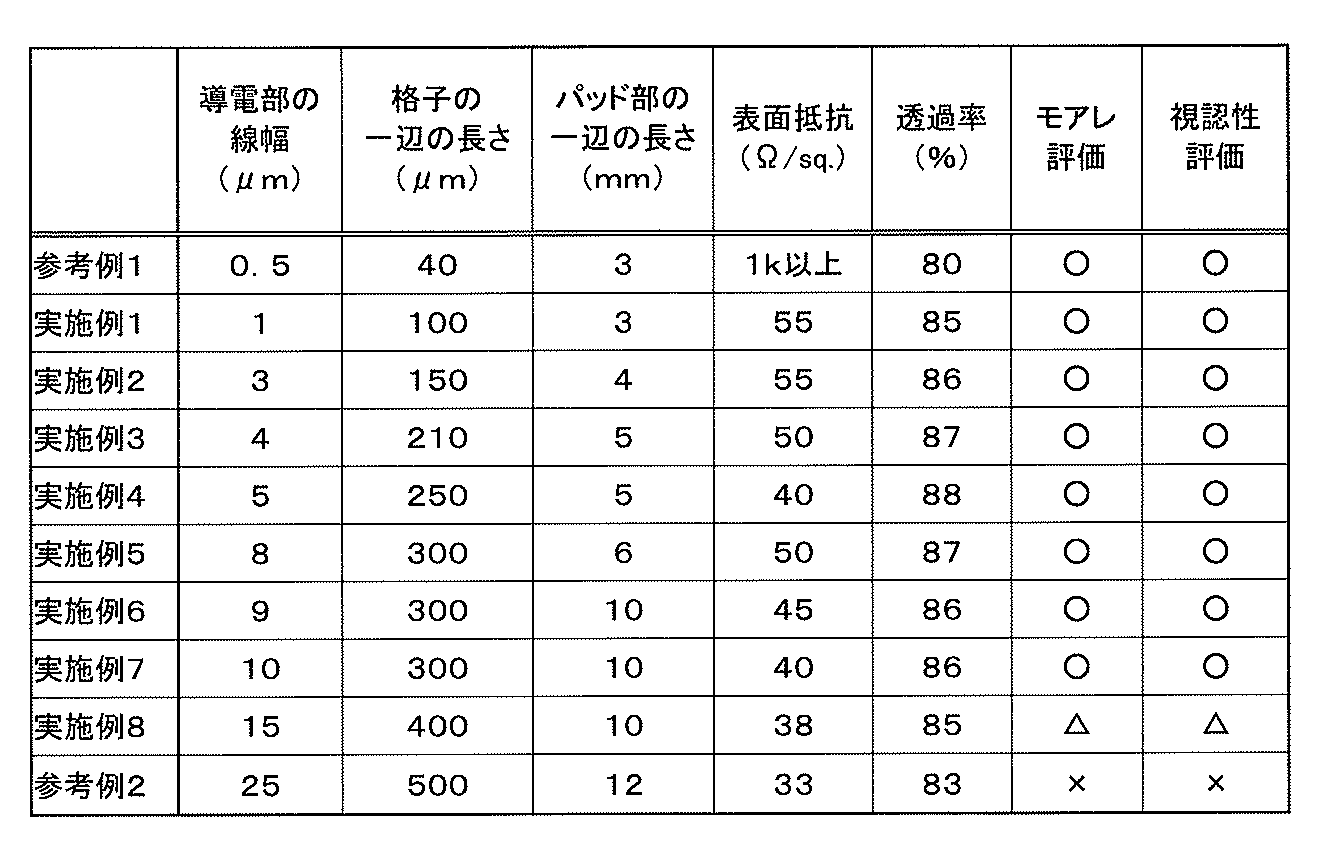
表3から、参考例1はモアレ及び視認性の評価は共に良好であったが、表面抵抗が1キロオーム/sq.以上であり、導電性が低く、検出感度が不十分になるおそれがある。参考例2は、導電性及び透過率共に良好であったが、モアレが顕在化し、導電部自体が肉眼で認識しやすくなり、視認性が劣化した。
これに対して、実施例1~8のうち、実施例1~7は、導電性、透過率、モアレ、視認性共に良好であった。実施例8はモアレの評価及び視認性の評価が実施例1~7よりも劣っているが、モアレが問題のないレベルでほんの少し見られる程度であり、表示装置の表示画像が見え難くなるということはなかった。
また、上述した実施例1~8に係る積層導電性フイルム50を用いてそれぞれ投影型静電容量方式のタッチパネルを作製した。指で触れて操作したところ、応答速度が速く、検出感度に優れることがわかった。また2点以上をタッチして操作したところ、同様に良好な結果が得られ、マルチタッチにも対応できることが確認できた。
本発明に係る導電性フイルム及びタッチパネルは、上述の実施の形態に限らず、本発明の要旨を逸脱することなく、種々の構成を採り得ることはもちろんである。
Claims (21)
- 基体(12A)と、
前記基体(12A)の一方の主面に形成された導電部(14A)とを有し、
前記導電部(14A)は、複数のパッド部(16A)がそれぞれ接続部(18A)を介して接続された金属細線による2以上の導電パターン(20A)を有し、
各前記パッド部(16A)は、一方の前記接続部(18A)から延びる第1渦巻き部(24A)と、他方の前記接続部(18A)から延びる第2渦巻き部(24B)と、前記第1渦巻き部(24A)と前記第2渦巻き部(24B)とを連結する連結部(26A)とを有し、
前記第1渦巻き部(24A)と前記第2渦巻き部(24B)とがそれぞれ複数の格子(28)が組み合わされて構成され、
前記連結部(26A)が複数の導線(30)にて構成されていることを特徴とする導電性フイルム。 - 請求項1記載の導電性フイルムにおいて、
前記第1渦巻き部(24A)及び前記第2渦巻き部(24B)の各周縁は、それぞれ前記格子(28)の頂点を山又は谷とする凹凸形状とされていることを特徴とする導電性フイルム。 - 請求項1記載の導電性フイルムにおいて、
前記連結部(26A)を構成する複数の前記導線(30)がそれぞれ直線状に形成されていることを特徴とする導電性フイルム。 - 請求項1記載の導電性フイルムにおいて、
前記導電パターン(20A)間に、前記導電パターン(20A)と非接続とされた金属細線によるダミーパターン(22A)が形成されていることを特徴とする導電性フイルム。 - 請求項4記載の導電性フイルムにおいて、
前記ダミーパターン(22A)は、一方の前記導電パターン(20A)における前記接続部(18A)と他方の前記導電パターン(20A)における前記接続部(18A)との間に配置されていることを特徴とする導電性フイルム。 - 請求項1記載の導電性フイルムにおいて、
前記第1渦巻き部(24A)及び前記第2渦巻き部(24B)の各周縁は、
前記格子(28)の一辺が連続して直線的に並ぶ2以上の長辺部(32A)と、
少なくとも1つの前記長辺部(32A)から直交して延びる金属細線による張り出し部(34A)とを有することを特徴とする導電性フイルム。 - 基体(12A)と、
前記基体(12A)の一方の主面に形成された第1導電部(14A)と、
前記基体(12A)の他方の主面に形成された第2導電部(14B)とを有し、
前記第1導電部(14A)は、複数の第1パッド部(16A)がそれぞれ第1接続部(18A)を介して接続された金属細線による2以上の第1導電パターン(20A)を有し、
前記第2導電部(14B)は、複数の第2パッド部(16B)がそれぞれ第2接続部(18B)を介して接続された金属細線による2以上の第2導電パターン(20B)を有し、
各前記第1パッド部(16A)は、一方の前記第1接続部(18A)から延びる第1渦巻き部(24A)と、他方の前記第1接続部(18A)から延びる第2渦巻き部(24B)と、前記第1渦巻き部(24A)と前記第2渦巻き部(24B)とを連結する第1連結部(26A)とを有し、
各前記第2パッド部(16B)は、一方の前記第2接続部(18B)から延びる第3渦巻き部(24C)と、他方の前記第2接続部(18B)から延びる第4渦巻き部(24D)と、前記第3渦巻き部(24C)と前記第4渦巻き部(24D)とを連結する第2連結部(26B)とを有し、
前記第1渦巻き部(24A)~前記第4渦巻き部(24D)とがそれぞれ複数の格子(28)が組み合わされて構成され、
前記第1連結部(26A)及び前記第2連結部(26B)が複数の導線(30)にて構成され、
前記第1導電パターン(20A)と前記第2導電パターン(20B)は、前記第1連結部(26A)と前記第2連結部(26B)とが略直交するように配置されていることを特徴とする導電性フイルム。 - 請求項7記載の導電性フイルムにおいて、
前記第1渦巻き部(24A)~前記第4渦巻き部(24D)の各周縁は、それぞれ前記格子(28)の頂点を山又は谷とする凹凸形状とされていることを特徴とする導電性フイルム。 - 請求項7記載の導電性フイルムにおいて、
前記第1導電パターン(20A)と前記第2導電パターン(20B)は、隣接する前記第1導電パターン(20A)間に前記第2接続部(18B)が位置し、隣接する前記第2導電パターン(20B)間に前記第1接続部(18A)が位置するように配置されていることを特徴とする導電性フイルム。 - 請求項7記載の導電性フイルムにおいて、
前記第1導電パターン(20A)と前記第2導電パターン(20B)は、前記第1導電パターン(20A)における前記第1渦巻き部(24A)と前記第2渦巻き部(24B)との間に、前記第2導電パターン(20B)における前記第3渦巻き部(24C)又は前記第4渦巻き部(24D)が位置し、前記第2導電パターン(20B)における前記第3渦巻き部(24C)と前記第4渦巻き部(24D)との間に、前記第1導電パターン(20A)における前記第1渦巻き部(24A)又は前記第2渦巻き部(24B)が位置するように配置されていることを特徴とする導電性フイルム。 - 請求項7記載の導電性フイルムにおいて、
前記第1導電パターン(20A)間に、前記第1導電パターン(20A)と非接続とされた金属細線による第1ダミーパターン(22A)が形成され、
前記第2導電パターン(20B)間に、前記第2導電パターン(20B)と非接続とされた金属細線による第2ダミーパターン(22B)が形成されていることを特徴とする導電性フイルム。 - 請求項11記載の導電性フイルムにおいて、
前記第1ダミーパターン(22A)は、一方の前記第1導電パターン(20A)における前記第1接続部(18A)と他方の前記第1導電パターン(20A)における前記第1接続部(18A)との間に配置され、
前記第2ダミーパターン(22B)は、一方の前記第2導電パターン(20B)における前記第2接続部(18B)と他方の前記第2導電パターン(20B)における前記第2接続部(18B)との間に配置されていることを特徴とする導電性フイルム。 - 請求項12記載の導電性フイルムにおいて、
前記第1導電パターン(20A)と前記第2導電パターン(20B)は、前記第1ダミーパターン(22A)間に前記第2接続部(18B)が位置し、前記第2ダミーパターン(22B)間に前記第1接続部(18A)が位置するように配置されていることを特徴とする導電性フイルム。 - 請求項7記載の導電性フイルムにおいて、
前記第1導電パターン(20A)の前記第1渦巻き部(24A)及び前記第2渦巻き部(24B)を構成する前記格子(28)の数が前記第2導電パターン(20B)の前記第3渦巻き部(24C)及び前記第4渦巻き部(24D)を構成する前記格子(28)の数よりも少ないことを特徴とする導電性フイルム。 - 請求項7記載の導電性フイルムにおいて、
前記第1渦巻き部(24A)及び前記第2渦巻き部(24B)の各周縁は、
前記格子(28)の一辺が連続して直線的に並ぶ2以上の第1長辺部(32A)と、
少なくとも1つの前記第1長辺部(32A)から直交して延びる金属細線による第1張り出し部(34A)とを有し、
前記第3渦巻き部(24C)及び前記第4渦巻き部(24D)の各周縁は、
前記格子(28)の一辺が連続して直線的に並ぶ2以上の第2長辺部(32B)と、
少なくとも1つの前記第2長辺部(32B)から直交して延びる金属細線による第2張り出し部(34B)とを有することを特徴とする導電性フイルム。 - 請求項15記載の導電性フイルムにおいて、
前記第1張り出し部(34A)が形成された前記第1長辺部(32A)と、前記第2張り出し部(34B)が形成されていない前記第2長辺部(32B)とが対向していることを特徴とする導電性フイルム。 - 請求項15記載の導電性フイルムにおいて、
前記第1張り出し部(34A)が形成されていない前記第1長辺部(32A)と、前記第2張り出し部(34B)が形成された前記第2長辺部(32B)とが対向していることを特徴とする導電性フイルム。 - 請求項1又は7記載の導電性フイルムにおいて、
各前記格子(28)の一辺の長さが100~400μmであることを特徴とする導電性フイルム。 - 請求項1又は7記載の導電性フイルムにおいて、
各前記格子(28)の線幅が1~15μmであることを特徴とする導電性フイルム。 - 表示装置(108)の表示パネル(110)上に設置された導電性フイルム(10A)を備えるタッチパネルであって、
前記導電性フイルム(10A)は、
基体(12A)と、
前記基体(12A)の一方の主面に形成された導電部(14A)とを有し、
前記導電部(14A)は、複数のパッド部(16A)がそれぞれ接続部(18A)を介して接続された金属細線による2以上の導電パターン(20A)を有し、
各前記パッド部(16A)は、一方の前記接続部(18A)から延びる第1渦巻き部(24A)と、他方の前記接続部(18A)から延びる第2渦巻き部(24B)と、前記第1渦巻き部(24A)と前記第2渦巻き部(24B)とを連結する連結部(26A)とを有し、
前記第1渦巻き部(24A)と前記第2渦巻き部(24B)とがそれぞれ複数の格子(28)が組み合わされて構成され、
前記連結部(26A)が複数の導線(30)にて構成されていることを特徴とするタッチパネル。 - 表示装置(108)の表示パネル(110)上に設置された導電性フイルム(50)を備えるタッチパネルであって、
前記導電性フイルム(50)は、
基体(12A)と、
前記基体(12A)の一方の主面に形成された第1導電部(14A)と、
前記基体(12A)の他方の主面に形成された第2導電部(14B)とを有し、
前記第1導電部(14A)は、複数の第1パッド部(16A)がそれぞれ第1接続部(18A)を介して接続された金属細線による2以上の第1導電パターン(20A)を有し、
前記第2導電部(14B)は、複数の第2パッド部(16B)がそれぞれ第2接続部(18B)を介して接続された金属細線による2以上の第2導電パターン(20B)を有し、
各前記第1パッド部(16A)は、一方の前記第1接続部(18A)から延びる第1渦巻き部(24A)と、他方の前記第1接続部(18A)から延びる第2渦巻き部(24B)と、前記第1渦巻き部(24A)と前記第2渦巻き部(24B)とを連結する第1連結部(26A)とを有し、
各前記第2パッド部(16B)は、一方の前記第2接続部(18B)から延びる第3渦巻き部(24C)と、他方の前記第2接続部(18B)から延びる第4渦巻き部(24D)と、前記第3渦巻き部(24C)と前記第4渦巻き部(24D)とを連結する第2連結部(26B)とを有し、
前記第1渦巻き部(24A)~前記第4渦巻き部(24D)とがそれぞれ複数の格子(28)が組み合わされて構成され、
前記第1連結部(26A)及び前記第2連結部(26B)が複数の導線(30)にて構成され、
前記第1導電パターン(20A)と前記第2導電パターン(20B)は、前記第1連結部(26A)と前記第2連結部(26B)とが略直交するように配置されていることを特徴とするタッチパネル。
Priority Applications (2)
| Application Number | Priority Date | Filing Date | Title |
|---|---|---|---|
| CN201280052278.2A CN103889708A (zh) | 2011-10-27 | 2012-10-25 | 导电性膜以及触摸面板 |
| US14/262,132 US20140232959A1 (en) | 2011-10-27 | 2014-04-25 | Conductive film and touch panel |
Applications Claiming Priority (2)
| Application Number | Priority Date | Filing Date | Title |
|---|---|---|---|
| JP2011235997A JP5698103B2 (ja) | 2011-10-27 | 2011-10-27 | 導電性フイルム及びタッチパネル |
| JP2011-235997 | 2011-10-27 |
Related Child Applications (1)
| Application Number | Title | Priority Date | Filing Date |
|---|---|---|---|
| US14/262,132 Continuation US20140232959A1 (en) | 2011-10-27 | 2014-04-25 | Conductive film and touch panel |
Publications (1)
| Publication Number | Publication Date |
|---|---|
| WO2013062041A1 true WO2013062041A1 (ja) | 2013-05-02 |
Family
ID=48167867
Family Applications (1)
| Application Number | Title | Priority Date | Filing Date |
|---|---|---|---|
| PCT/JP2012/077589 Ceased WO2013062041A1 (ja) | 2011-10-27 | 2012-10-25 | 導電性フイルム及びタッチパネル |
Country Status (5)
| Country | Link |
|---|---|
| US (1) | US20140232959A1 (ja) |
| JP (1) | JP5698103B2 (ja) |
| CN (1) | CN103889708A (ja) |
| TW (1) | TW201324280A (ja) |
| WO (1) | WO2013062041A1 (ja) |
Cited By (3)
| Publication number | Priority date | Publication date | Assignee | Title |
|---|---|---|---|---|
| CN103440906A (zh) * | 2013-07-31 | 2013-12-11 | 南昌欧菲光科技有限公司 | 导电膜及触控面板 |
| EP2905683A1 (en) * | 2014-02-05 | 2015-08-12 | LG Innotek Co., Ltd. | Capacitive touch window |
| TWI564767B (zh) * | 2014-08-13 | 2017-01-01 | 財團法人工業技術研究院 | 感測結構及其製作方法 |
Families Citing this family (13)
| Publication number | Priority date | Publication date | Assignee | Title |
|---|---|---|---|---|
| US9594454B2 (en) * | 2013-03-29 | 2017-03-14 | Sharp Kabushiki Kaisha | Touch-panel substrate and electronic device |
| JP2015200720A (ja) | 2014-04-04 | 2015-11-12 | 株式会社ジャパンディスプレイ | 表示装置、温度情報取得装置及び温度情報取得方法 |
| US9927939B2 (en) * | 2014-08-13 | 2018-03-27 | Samsung Display Co., Ltd. | Touch panel and display apparatus including the same |
| CN107111394B (zh) * | 2014-11-27 | 2020-01-10 | 富士胶片株式会社 | 导电性薄膜及具备该导电性薄膜的触摸面板传感器 |
| JP2016143725A (ja) * | 2015-01-30 | 2016-08-08 | イビデン株式会社 | プリント配線板およびその製造方法 |
| JP2016143727A (ja) * | 2015-01-30 | 2016-08-08 | イビデン株式会社 | プリント配線板およびその製造方法 |
| TWI610204B (zh) * | 2015-02-27 | 2018-01-01 | Fujikura Ltd | 配線體、配線基板以及碰觸偵知器 |
| KR102160020B1 (ko) * | 2015-07-24 | 2020-09-25 | 후지필름 가부시키가이샤 | 터치 패널용 도전 필름, 터치 패널, 및 터치 패널 부착 표시 장치 |
| JP6889849B2 (ja) * | 2016-07-05 | 2021-06-18 | 大日本印刷株式会社 | 導電性パターンシート、導電性パターンシート用中間部材およびその製造方法 |
| CN107275512A (zh) * | 2017-05-25 | 2017-10-20 | 厦门天马微电子有限公司 | 一种有机电致发光显示面板、其制作方法及显示装置 |
| KR102402040B1 (ko) * | 2017-12-21 | 2022-05-26 | 삼성디스플레이 주식회사 | 전자 장치 및 이의 제조방법 |
| KR102883426B1 (ko) | 2019-07-30 | 2025-11-07 | 엘지디스플레이 주식회사 | 터치 디스플레이 장치 |
| CN111796705B (zh) * | 2020-05-22 | 2022-05-17 | 江西卓讯微电子有限公司 | 面板及其制备方法、触控显示屏和电子设备 |
Citations (4)
| Publication number | Priority date | Publication date | Assignee | Title |
|---|---|---|---|---|
| US20040239650A1 (en) * | 2003-06-02 | 2004-12-02 | Mackey Bob Lee | Sensor patterns for a capacitive sensing apparatus |
| US7202859B1 (en) * | 2002-08-09 | 2007-04-10 | Synaptics, Inc. | Capacitive sensing pattern |
| WO2011093420A1 (ja) * | 2010-01-28 | 2011-08-04 | 富士フイルム株式会社 | 導電シート、導電シートの使用方法及びタッチパネル |
| JP2011175412A (ja) * | 2010-02-24 | 2011-09-08 | Shin Etsu Polymer Co Ltd | 静電容量式のタッチパネルスイッチ |
Family Cites Families (5)
| Publication number | Priority date | Publication date | Assignee | Title |
|---|---|---|---|---|
| US4578654A (en) * | 1983-11-16 | 1986-03-25 | Minnesota Mining And Manufacturing Company | Distributed capacitance lc resonant circuit |
| GB2428306B (en) * | 2005-07-08 | 2007-09-26 | Harald Philipp | Two-dimensional capacitive position sensor |
| JP4821544B2 (ja) * | 2006-09-28 | 2011-11-24 | カシオ計算機株式会社 | 電磁誘導型タッチパネルを備えた液晶表示装置 |
| CN101866254A (zh) * | 2010-04-09 | 2010-10-20 | 鸿富锦精密工业(深圳)有限公司 | 电阻式触控屏及其显示装置 |
| CN103164093A (zh) * | 2011-12-19 | 2013-06-19 | 禾瑞亚科技股份有限公司 | 一种电容式触摸屏 |
-
2011
- 2011-10-27 JP JP2011235997A patent/JP5698103B2/ja not_active Expired - Fee Related
-
2012
- 2012-10-25 CN CN201280052278.2A patent/CN103889708A/zh active Pending
- 2012-10-25 WO PCT/JP2012/077589 patent/WO2013062041A1/ja not_active Ceased
- 2012-10-26 TW TW101139767A patent/TW201324280A/zh unknown
-
2014
- 2014-04-25 US US14/262,132 patent/US20140232959A1/en not_active Abandoned
Patent Citations (4)
| Publication number | Priority date | Publication date | Assignee | Title |
|---|---|---|---|---|
| US7202859B1 (en) * | 2002-08-09 | 2007-04-10 | Synaptics, Inc. | Capacitive sensing pattern |
| US20040239650A1 (en) * | 2003-06-02 | 2004-12-02 | Mackey Bob Lee | Sensor patterns for a capacitive sensing apparatus |
| WO2011093420A1 (ja) * | 2010-01-28 | 2011-08-04 | 富士フイルム株式会社 | 導電シート、導電シートの使用方法及びタッチパネル |
| JP2011175412A (ja) * | 2010-02-24 | 2011-09-08 | Shin Etsu Polymer Co Ltd | 静電容量式のタッチパネルスイッチ |
Cited By (5)
| Publication number | Priority date | Publication date | Assignee | Title |
|---|---|---|---|---|
| CN103440906A (zh) * | 2013-07-31 | 2013-12-11 | 南昌欧菲光科技有限公司 | 导电膜及触控面板 |
| EP2905683A1 (en) * | 2014-02-05 | 2015-08-12 | LG Innotek Co., Ltd. | Capacitive touch window |
| US9778801B2 (en) | 2014-02-05 | 2017-10-03 | Lg Innotek Co., Ltd. | Touch window |
| US10019124B2 (en) | 2014-02-05 | 2018-07-10 | Lg Innotek Co., Ltd. | Touch window |
| TWI564767B (zh) * | 2014-08-13 | 2017-01-01 | 財團法人工業技術研究院 | 感測結構及其製作方法 |
Also Published As
| Publication number | Publication date |
|---|---|
| JP2013091298A (ja) | 2013-05-16 |
| CN103889708A (zh) | 2014-06-25 |
| TW201324280A (zh) | 2013-06-16 |
| JP5698103B2 (ja) | 2015-04-08 |
| US20140232959A1 (en) | 2014-08-21 |
Similar Documents
| Publication | Publication Date | Title |
|---|---|---|
| JP5698103B2 (ja) | 導電性フイルム及びタッチパネル | |
| JP5839541B2 (ja) | 導電シート及びタッチパネル | |
| JP5728412B2 (ja) | 導電シート及びタッチパネル | |
| JP5670827B2 (ja) | 導電シート及びタッチパネル | |
| JP5676225B2 (ja) | 導電シート、導電シートの使用方法及び静電容量方式タッチパネル | |
| JP5615856B2 (ja) | 導電シート及びタッチパネル | |
| JP5248653B2 (ja) | 導電シート及び静電容量方式タッチパネル | |
| JP5809846B2 (ja) | 導電シート及びタッチパネル | |
| JP4820451B2 (ja) | 導電シート、導電シートの使用方法及びタッチパネル | |
| JP5638027B2 (ja) | 導電シート及び静電容量方式タッチパネル | |
| JP5675491B2 (ja) | 導電シート及びタッチパネル | |
| JP5507343B2 (ja) | タッチパネル及び導電シート | |
| JP5638459B2 (ja) | タッチパネル及び導電シート | |
| JP2012014669A (ja) | 導電シート、導電シートの使用方法及び静電容量方式タッチパネル | |
| JP2013149232A (ja) | 導電シート及びタッチパネル | |
| JP5890063B2 (ja) | 導電フィルム | |
| JP2011113149A (ja) | 導電シート、導電シートの使用方法及び静電容量方式タッチパネル | |
| JP5613448B2 (ja) | タッチパネル及び導電シート | |
| JP5711606B2 (ja) | 導電性シート及びタッチパネル | |
| JP5476237B2 (ja) | タッチパネル及び導電シート |
Legal Events
| Date | Code | Title | Description |
|---|---|---|---|
| 121 | Ep: the epo has been informed by wipo that ep was designated in this application |
Ref document number: 12843049 Country of ref document: EP Kind code of ref document: A1 |
|
| NENP | Non-entry into the national phase |
Ref country code: DE |
|
| 122 | Ep: pct application non-entry in european phase |
Ref document number: 12843049 Country of ref document: EP Kind code of ref document: A1 |