WO2013061730A1 - Élément à capacité électrostatique et circuit résonant - Google Patents
Élément à capacité électrostatique et circuit résonant Download PDFInfo
- Publication number
- WO2013061730A1 WO2013061730A1 PCT/JP2012/075488 JP2012075488W WO2013061730A1 WO 2013061730 A1 WO2013061730 A1 WO 2013061730A1 JP 2012075488 W JP2012075488 W JP 2012075488W WO 2013061730 A1 WO2013061730 A1 WO 2013061730A1
- Authority
- WO
- WIPO (PCT)
- Prior art keywords
- electrode
- internal electrode
- capacitance element
- internal
- capacitor
- Prior art date
Links
Images


Classifications
-
- H—ELECTRICITY
- H01—ELECTRIC ELEMENTS
- H01G—CAPACITORS; CAPACITORS, RECTIFIERS, DETECTORS, SWITCHING DEVICES OR LIGHT-SENSITIVE DEVICES, OF THE ELECTROLYTIC TYPE
- H01G7/00—Capacitors in which the capacitance is varied by non-mechanical means; Processes of their manufacture
-
- H—ELECTRICITY
- H01—ELECTRIC ELEMENTS
- H01G—CAPACITORS; CAPACITORS, RECTIFIERS, DETECTORS, SWITCHING DEVICES OR LIGHT-SENSITIVE DEVICES, OF THE ELECTROLYTIC TYPE
- H01G4/00—Fixed capacitors; Processes of their manufacture
- H01G4/30—Stacked capacitors
-
- H—ELECTRICITY
- H01—ELECTRIC ELEMENTS
- H01G—CAPACITORS; CAPACITORS, RECTIFIERS, DETECTORS, SWITCHING DEVICES OR LIGHT-SENSITIVE DEVICES, OF THE ELECTROLYTIC TYPE
- H01G4/00—Fixed capacitors; Processes of their manufacture
- H01G4/002—Details
- H01G4/018—Dielectrics
- H01G4/06—Solid dielectrics
- H01G4/08—Inorganic dielectrics
- H01G4/12—Ceramic dielectrics
-
- H—ELECTRICITY
- H01—ELECTRIC ELEMENTS
- H01G—CAPACITORS; CAPACITORS, RECTIFIERS, DETECTORS, SWITCHING DEVICES OR LIGHT-SENSITIVE DEVICES, OF THE ELECTROLYTIC TYPE
- H01G4/00—Fixed capacitors; Processes of their manufacture
- H01G4/002—Details
- H01G4/228—Terminals
- H01G4/232—Terminals electrically connecting two or more layers of a stacked or rolled capacitor
-
- H—ELECTRICITY
- H01—ELECTRIC ELEMENTS
- H01G—CAPACITORS; CAPACITORS, RECTIFIERS, DETECTORS, SWITCHING DEVICES OR LIGHT-SENSITIVE DEVICES, OF THE ELECTROLYTIC TYPE
- H01G7/00—Capacitors in which the capacitance is varied by non-mechanical means; Processes of their manufacture
- H01G7/06—Capacitors in which the capacitance is varied by non-mechanical means; Processes of their manufacture having a dielectric selected for the variation of its permittivity with applied voltage, i.e. ferroelectric capacitors
Definitions
- the present invention relates to a capacitive element and a resonance circuit including the capacitive element.
- the inventors of the present invention provide a capacitor element formed by laminating a plurality of internal electrodes by providing an irrelevant internal electrode in the capacitor element body that forms a capacitance as a stress control unit, and by the residual stress generated during firing.
- a technique for improving electrical characteristics has been proposed (Patent Document 1).
- Patent Document 1 by providing a stress control unit formed by laminating internal electrodes on the upper and lower sides of a capacitive element body, internal stress caused by contraction of a dielectric layer during firing of the capacitive element is reduced. It can be generated in the dielectric layer of the body. As a result, the relative dielectric constant of the dielectric layer of the capacitive element body can be increased.
- the dielectric constant can be improved and the capacitance can be increased by utilizing the residual stress generated during firing. For this reason, if this residual stress can be further increased, the capacitance element can be further reduced in size.
- the present disclosure aims to improve electrical characteristics in a capacitive element. It is another object of the present invention to provide a resonance circuit with excellent reliability by using the capacitance element.
- An electrostatic capacitance element of the present disclosure is formed on a side surface of a capacitive element body including a dielectric layer and at least a pair of internal electrodes formed with the dielectric layer interposed therebetween. External terminals connected to each other. The stress generated due to the difference in linear expansion coefficient between the dielectric layer and the internal electrode is concentrated at the center of the capacitor formed by the dielectric layer and the pair of internal electrodes sandwiching the dielectric layer. Has been.
- stress is concentrated at the center of the capacitor, and thus the capacitance per unit volume increases.
- the resonance circuit of the present disclosure includes a resonance capacitor including the capacitance element and a resonance coil connected to the resonance capacitor.
- the residual stress in the electrostatic capacitance element increases, thereby improving the electrical characteristics.
- FIG. 1A is a perspective view of a variable capacitance element according to the first embodiment of the present disclosure
- FIG. 1B is a cross-sectional configuration diagram of the variable capacitance element.
- FIG. 3 is a plan configuration diagram of an internal electrode constituting the variable capacitance element according to the first embodiment of the present disclosure.
- FIG. 3 is a plan view of two internal electrodes formed in the variable capacitance element according to the first embodiment of the present disclosure as seen from above.
- 6 is a plan configuration diagram of internal electrodes of a variable capacitance element according to Comparative Example 1.
- FIG. 6 is a plan configuration diagram of internal electrodes of a variable capacitance element according to Comparative Example 2.
- FIG. 10 is a plan configuration diagram of internal electrodes that constitute a variable capacitance element according to Modification 1-1.
- FIG. 12 is a plan configuration diagram of internal electrodes that constitute a variable capacitance element according to Modification 1-2.
- FIG. 10 is a plan configuration diagram of internal electrodes that constitute a variable capacitance element according to Modification 1-3.
- FIG. 10 is a plan configuration diagram of internal electrodes that constitute a variable capacitance element according to Modification 1-4. It is a plane lineblock diagram of an internal electrode which constitutes a variable capacity element concerning a 2nd embodiment of this indication.
- FIG. 10 is a plan configuration diagram of internal electrodes that constitute a variable capacitance element according to Modification 2-1.
- FIG. 10 is a plan configuration diagram of internal electrodes that constitute a variable capacitance element according to Modification 2-2. It is a plane lineblock diagram of the internal electrode which constitutes the variable capacity element concerning a 3rd embodiment of this indication.
- FIG. 10 is a plan configuration diagram of internal electrodes that constitute a variable capacitance element according to Modification 3-1.
- FIG. 10 is a plan configuration diagram of internal electrodes that constitute a variable capacitance element according to Modification 3-2.
- FIG. 10 is a plan configuration diagram of internal electrodes constituting a variable capacitance element according to Modification 3-3. It is an external appearance perspective view of the variable capacitance element which concerns on 4th Embodiment of this indication.
- 14 is an external perspective view of a variable capacitor according to Modification 4-1.
- FIG. 1 is a plan configuration diagram of internal electrodes that constitute a variable capacitance element according to Modification 2-2. It is a plane lineblock diagram of the internal electrode which constitutes the variable capacity element concerning a 3r
- FIG. 10 is a plan configuration diagram of a dielectric layer and internal electrodes that constitute a variable capacitance element according to Modification 4-2.
- FIG. 10 is a plan configuration diagram of a dielectric layer and internal electrodes constituting a variable capacitance element according to Modification 4-3.
- FIG. 14 is a plan configuration diagram of a dielectric layer and internal electrodes constituting a variable capacitance element according to Modification 4-4.
- FIG. 10 is a plan configuration diagram of a dielectric layer and internal electrodes that constitute a variable capacitance element according to Modification 4-5.
- FIG. 10 is a plan configuration diagram of a dielectric layer and internal electrodes constituting a variable capacitance element according to Modification 4-6.
- FIG. 10 is a plan configuration diagram of a dielectric layer and internal electrodes constituting a variable capacitance element according to Modification 4-7.
- FIG. 10 is a plan configuration diagram of a dielectric layer and internal electrodes constituting a variable capacitance element according to Modification 4-8. It is a plane lineblock diagram of the dielectric material layer and internal electrode which constitute the variable capacity element concerning a 5th embodiment of this indication.
- FIG. 10 is a plan configuration diagram of a dielectric layer and internal electrodes that constitute a variable capacitance element according to Modification 5-1.
- FIG. 10 is a plan view of two internal electrodes of a variable capacitance element according to Modification 5-1 as seen from above.
- FIG. 12 is a plan configuration diagram of a dielectric layer and internal electrodes constituting a variable capacitance element according to Modification 5-2.
- FIG. 15 is a plan configuration diagram of a dielectric layer and internal electrodes constituting a variable capacitance element according to Modification 5-3. It is an external appearance perspective view of the variable capacitance element concerning a 6th embodiment of this indication. It is a plane lineblock diagram of an internal electrode which constitutes a variable capacity element concerning a 6th embodiment of this indication. It is a figure when the variable capacitance element main body which concerns on 6th Embodiment of this indication is seen through from the upper surface.
- FIG. 10 is a plan configuration diagram of a dielectric layer and internal electrodes constituting a variable capacitance element according to Modification 6-1.
- FIG. 12 is a plan configuration diagram of a dielectric layer and internal electrodes constituting a variable capacitance element according to Modification 6-2.
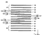
- FIG. 36A is a schematic perspective view of a variable capacitance element according to a seventh embodiment of the present disclosure
- FIG. 36B is a cross-sectional configuration diagram of the variable capacitance element. It is an exploded view when the variable capacitance element main body which concerns on 7th Embodiment is seen from one side surface of a long side direction.
- FIG. 38A is a plan configuration diagram when the first internal electrode 88 is viewed from above
- FIG. 38B is a configuration diagram when the first internal electrode 88 is viewed from one side surface.
- FIG. 38A is a plan configuration diagram when the first internal electrode 88 is viewed from above
- FIG. 38B is a configuration diagram when the first internal electrode 88 is viewed from one side surface.
- FIG. 39A is a plan configuration diagram when the second internal electrode 89 is viewed from above, and FIG. 39B is a configuration diagram when the second internal electrode 89 is viewed from one side surface.
- FIG. 40A is a plan configuration diagram when the fourth internal electrode 91 is viewed from the top surface, and FIG. 40B is a configuration diagram when the fourth internal electrode 91 is viewed from one side surface.
- It is a circuit block diagram of the voltage control circuit incorporating the variable capacitance element which concerns on 7th Embodiment.
- FIG. 14 is an exploded view of a variable capacitor element body of a variable capacitor according to Modification 7-1 when viewed from one side surface in the long side direction.
- FIG. 14 is an exploded view of a variable capacitance element body of a variable capacitance element according to Modification 7-2 when viewed from one side surface in the long side direction.
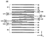
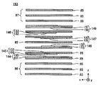
- FIG. 44A is a schematic perspective view of a variable capacitance element according to an eighth embodiment of the present disclosure
- FIG. 44B is a cross-sectional configuration diagram of the variable capacitance element. It is an exploded view when the variable capacitance element main body which concerns on 8th Embodiment of this indication is seen from one side surface of a long side direction.
- 46A is a plan configuration diagram when the first internal electrode 123 is viewed from the top surface
- FIG. 46B is a configuration diagram when the first internal electrode 123 is viewed from one side surface.
- FIG. 47A is a plan configuration diagram when the second internal electrode 124 is viewed from above, and FIG. 47B is a configuration diagram when the second internal electrode 124 is viewed from one side surface.
- 48A is a plan configuration diagram when the fourth internal electrode 126 is viewed from the top surface, and FIG. 48B is a configuration diagram when the fourth internal electrode 126 is viewed from one side surface.
- FIG. 20 is a configuration diagram of a variable capacitance element according to an eighth embodiment of the present disclosure as viewed through the first internal electrode to the sixth internal electrode from above. It is a circuit block diagram of the voltage control circuit incorporating the variable capacitance element which concerns on 8th Embodiment.
- FIG. 20 is a configuration diagram of a variable capacitance element according to an eighth embodiment of the present disclosure as viewed through the first internal electrode to the sixth internal electrode from above. It is a circuit block diagram of the voltage control circuit incorporating the variable capacitance element which concerns on 8th Embodiment.
- FIG. 20 is a configuration diagram
- FIG. 16 is an exploded view of a variable capacitance element body of a variable capacitance element according to Modification 8-1 when viewed from one side surface in the long side direction.
- 52A is a schematic perspective view of a variable capacitance element according to the ninth embodiment of the present disclosure
- FIG. 52B is a cross-sectional configuration diagram of the variable capacitance element. It is an exploded view when the variable-capacitance element main body which concerns on 9th Embodiment of this indication is seen from one side surface of a long side direction.
- 54A is a plan configuration diagram when the first internal electrode 144 is viewed from above
- FIG. 53B is a configuration diagram when the first internal electrode 144 is viewed from one side surface.
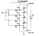
- FIG. 30 is a configuration diagram of the variable capacitance element according to the ninth embodiment of the present disclosure as viewed through the first internal electrode to the sixth internal electrode from above. It is a circuit block diagram of the voltage control circuit incorporating the variable capacitance element which concerns on 9th Embodiment.
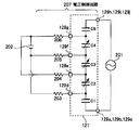
- FIG. 16 is an exploded view of the variable capacitor element body of the variable capacitor according to Modification 9-1 when viewed from one side surface in the long side direction. It is a block block diagram of the receiving system circuit part of the non-contact IC card using the resonance circuit which concerns on 10th Embodiment of this indication.
- Fifth Embodiment Variable capacitance element in which the outer shape of the variable capacitance element main body and the electrode main body constituting the capacitance have the same shape. 6.
- Sixth Embodiment Variable capacitance element in which a plurality of connection electrodes are formed in one internal electrode.
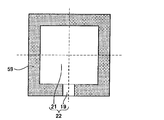
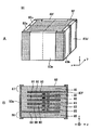
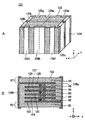
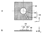
- FIG. 1A is a perspective view of a variable capacitor according to this embodiment
- FIG. 1B is a cross-sectional configuration diagram of the variable capacitor according to this embodiment
- FIG. 2 is a plan configuration diagram of internal electrodes constituting the variable capacitance element of this embodiment. 1A and 2, a line passing through the center of gravity of the internal electrode and the dielectric layer is indicated by a broken line. The same applies to the following drawings.
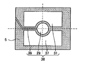
- variable capacitance element 1 of the present embodiment example is composed of a variable capacitance element body 2 constituted by a rectangular parallelepiped member and two external terminals 3 and 4.
- the variable capacitance element body 2 is composed of two internal electrodes 10 stacked via a dielectric layer 5, and a lower dielectric layer 6 is formed below the two internal electrodes 10.
- the upper dielectric layer 7 is laminated on the upper layer.
- the lower dielectric layer 6 and the upper dielectric layer 7 do not expose the surface of the internal electrode 10.
- the variable capacitance element body 2 has a structure in which a sheet-like dielectric layer 5 in which a conductive layer constituting the internal electrode 10 is formed on one surface is laminated, and each dielectric formed in a sheet shape.
- the layer 5 has a rectangular shape on a plane on which the internal electrode 10 is formed.
- the dielectric layer 5 is made of a ferroelectric material in order to constitute the variable capacitance element 1 whose capacitance changes according to the applied voltage.
- a ferroelectric material specifically, a dielectric material that generates ionic polarization can be used.
- a ferroelectric material that causes ion polarization is a ferroelectric material that is made of an ionic crystal material and is electrically polarized by the displacement of positive and negative ion atoms.
- a ferroelectric material that generates ionic polarization is represented by the chemical formula ABO 3 (O is an oxygen element) and has a perovskite structure, where A and B are two predetermined elements.
- ferroelectric material examples include barium titanate (BaTiO 3 ), potassium niobate (KNbO 3 ), lead titanate (PbTiO 3 ), and the like.
- PZT lead zirconate titanate in which lead zirconate (PbZrO 3 ) is mixed with lead titanate (PbTiO 3 ) may be used as a material for forming the dielectric layer 5.
- ferroelectric material a ferroelectric material that generates electronic polarization may be used.
- this ferroelectric material an electric dipole moment is generated in a portion biased to a positive charge and a portion biased to a negative charge, and polarization occurs.
- a rare earth iron oxide having a ferroelectric property by forming polarization by forming a charge surface of Fe 2+ and a charge surface of Fe 3+ has been reported.
- the rare earth element is RE and the iron group element is TM
- the material represented by the molecular formula (RE) ⁇ (TM) 2 ⁇ O 4 (O: oxygen element) has a high dielectric constant. It has been reported.
- rare earth elements include Y, Er, Yb, and Lu (particularly Y and heavy rare earth elements), and examples of iron group elements include Fe, Co, and Ni (particularly Fe).
- iron group elements include Fe, Co, and Ni (particularly Fe).
- (RE) ⁇ (TM) 2 ⁇ O 4 include ErFe 2 O 4 , LuFe 2 O 4 , and YFe 2 O 4 .
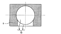
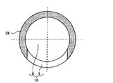
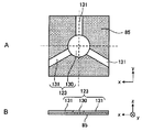
- the internal electrode 10 includes a circular electrode body 8, and a connection electrode 9 that is connected to the electrode body 8 and has an end portion exposed to the side surface of the variable capacitor element body 2. It consists of The center of gravity of the electrode body 8 of the internal electrode 10 is formed so as to be positioned at the center of the dielectric layer 5 formed in a sheet shape.
- the internal electrode 10 can be formed using, for example, a conductive paste containing fine metal powder (Pd, Pd / Ag, Ni, etc.).
- the two internal electrodes 10 are formed of the same material.
- the present disclosure is not limited to this, and for example, the internal electrodes 10 formed of different materials may be stacked depending on applications.
- connection electrodes 9 constituting each internal electrode 10 are arranged so as to face each other. That is, one internal electrode 10 has a configuration in which the other internal electrode 10 is rotated 180 degrees around an axis perpendicular to the electrode surface. In the variable capacitor element body 2, the connection electrode 9 is provided on the opposite side surface. Exposed.
- the external terminals 3 and 4 are formed on the side surface of the variable capacitance element body 2 and are electrically connected to the exposed connection electrodes 9. That is, in the present embodiment example, the two external terminals 3 and 4 are formed on two opposing sides of the variable capacitance element body 2. The two external terminals 3 and 4 are formed so as to cover the side surface of the variable capacitor element body 2 in the stacking direction of the internal electrodes 10 and to protrude from the upper surface and the lower surface of the variable capacitor element body 2.
- the capacitor C is formed between the two electrode bodies 8 facing each other. Then, by applying a desired voltage between the two external terminals 3 and 4, the relative dielectric constant of the dielectric layer 5 between the electrode bodies 8 can be varied.
- a dielectric sheet made of a desired dielectric material is prepared.
- the dielectric sheet constitutes each dielectric layer 5 in the variable capacitance element body 2 and has a thickness of about 2.5 ⁇ m, for example.
- These dielectric sheets can be formed by applying a paste-like dielectric material on a PET (polyethylene terephthalate) film to a desired thickness.
- a mask is prepared in which a region corresponding to the formation region of the internal electrode 10 shown in FIG. 2 is opened.
- a conductive paste obtained by pasting metal fine powders such as Pt, Pd, Pd / Ag, Ni, and Ni alloy is prepared. Then, the conductive paste is applied (silk printing) to one surface of the dielectric sheet through the respective masks prepared in the previous stage. Thereby, the dielectric sheet
- the respective dielectric sheets on which the internal electrodes 10 are formed are laminated in a desired order with the directions of the surfaces on which the respective electrodes are printed aligned.
- the two internal electrodes 10 are stacked so that the sides and the centers of the electrode bodies overlap in the stacking direction.
- dielectric sheets on which no electrodes are printed are stacked on top and bottom of the stacked body and are bonded by pressure.
- variable capacitance element body 2 is manufactured. Thereafter, the two external terminals 3 and 4 are attached to predetermined positions on the side surface of the variable capacitance element body 2. In this embodiment, the variable capacitance element 1 is manufactured in this way.
- variable capacitance element 1 of the present embodiment example residual stress (compressive stress) is generated due to a difference in shrinkage rate when the dielectric material and the electrode material are sintered. This residual stress is generated in the direction in which the electrode material and the dielectric material contract in each layer.
- the two electrode bodies 8 constituting the capacitor C have the same shape, and are stacked so that each side and center overlap in the stacking direction of the internal electrodes 10. Furthermore, the electrode body 8 is formed so that the center thereof coincides with the center of the dielectric layer 5. For this reason, in the variable capacitance element 1 of the present embodiment example, each internal electrode 10 and the dielectric layer 5 contract toward the center thereof. Thereby, the residual stress generated at the time of sintering can be concentrated on the center of the capacitor C formed by the two internal electrodes 10.
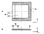
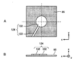
- FIG. 3 is a plan view of the two internal electrodes 10 formed in the variable capacitance element 1 of this embodiment as seen through the top surface.
- the direction and magnitude of the residual stress generated in the lower internal electrode 10 is indicated by an arrow a
- the direction and magnitude of the residual stress generated in the upper internal electrode 10 is indicated by an arrow b.
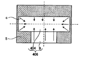
- FIG. 4 shows a planar configuration of the internal electrode 406 of the variable capacitance element according to Comparative Example 1
- FIG. 5 shows a planar configuration of the internal electrode 403 of the variable capacitance element according to Comparative Example 2.
- Comparative Example 1 and Comparative Example 2 only the shape of the electrode main body forming the capacitor is different from that of the variable capacitance element 1 of the present embodiment.
- the shape of the electrode main body 404 is rectangular as shown in FIG. 4, and in Comparative Example 2, the shape of the electrode main body 401 is square as shown in FIG.
- the direction and magnitude of the residual stress generated during firing are indicated by an arrow c
- FIG. 5 the direction and magnitude of the residual stress generated during firing are indicated by an arrow d.
- the shape of the electrode body 404 of the internal electrode 406 is rectangular as shown in FIG. For this reason, the residual stress generated during firing is indicated by an arrow c in the electrode body 40.
- the residual stress generated from the long side direction 4 differs from the residual stress generated from the short side direction.
- the electrode body 404 has a shape with low symmetry in the electrode surface, there are few components of the residual stress toward the center of gravity. Furthermore, when the magnitude of the residual stress generated on the side where the connection electrode 9 is formed is taken into consideration, the magnitude of the residual stress generated in the internal electrode 406 and the direction in which it occurs are varied.
- the shape of the electrode body 401 of the internal electrode 403 is square as shown in FIG. For this reason, the residual stress generated during firing is affected by the residual stress generated on the side where the connection electrode 9 is formed, as shown by an arrow d, and the residual stress generated in the internal electrode 403 is biased in the plane, It becomes larger on the connection electrode 9 side. Further, since the electrode body 404 has a shape with low symmetry in the electrode plane, the component of the residual stress toward the center of gravity is small.
- the shape of the electrode body 8 of the internal electrode 10 is circular. For this reason, it is a shape with high in-plane symmetry, and the residual stress (compressive stress) which generate
- the residual stress generated from the side where the connection electrode 9 is formed toward the center increases.
- the shape of the electrode body 8 is formed in a circular shape, the change in the residual stress is gentle in the internal electrode 10, and the residual stress generated on the side where the connection electrode 9 is formed is also the center of gravity of the electrode body 8. Occurs towards.
- the residual stress concentrates toward the center of the electrode body 8 that forms the capacity of the internal electrode 10, so that the tensile stress in the stacking direction (electric field direction) of the internal electrode 10 can be further increased.
- electrical characteristics such as an increase in capacitance per unit volume of the capacitor and an increase in variable rate can be improved.
- the shape of the electrode body 8 of the internal electrode 10 is formed in a circular shape, but the same effect can be obtained if the shape is highly symmetrical with respect to an axis that passes through the center of gravity of the electrode body 8 and is horizontal to the electrode surface. be able to. By the way, there are an infinite number of axes that pass through the center of gravity of the electrode body 8 and are horizontal to the electrode surface.
- “high symmetry” means that the electrode shape overlaps with a smaller rotation angle (or substantially). It means an electrode shape that can be overlapped).
- the shape of the electrode body 8 having high symmetry in the case of a regular pentagon, it overlaps with the original electrode shape even when rotated by 72 degrees, and it can be said that rotational symmetry is high. Therefore, it is preferable to have an arbitrary shape or a shape having a rotation of 72 degrees or less. Any shape that has high symmetry in either line symmetry or rotational symmetry may be used, but it is more preferable that both shapes have high symmetry. Below, the modification of the variable capacitance element of this embodiment is shown.
- FIG. 6 shows a planar configuration of the internal electrodes constituting the variable capacitance element according to Modification 1-1.
- the electrode body 11 of the internal electrode 12 has an elliptical shape.
- the major axis direction of the ellipse is configured as the major axis direction of the dielectric layer 5
- the minor axis direction is configured as the minor axis direction of the dielectric layer 5.
- the internal electrode 12 shown in FIG. 6 is laminated in two layers so that the sides and the center of the electrode body 11 overlap in the lamination direction, and the connection electrodes 9 face each other.
- the variable capacitance element body is configured so as to be exposed on the side surface. Then, by providing an external terminal that is electrically connected to each connection electrode 9 exposed at substantially the center in the major axis direction of the variable capacitor element body, the variable capacitor element of Modification 1-3 is formed.
- a capacitor is constituted by a pair of stacked electrode bodies 11.
- the electrode body 11 constituting the capacitor has an elliptical shape with high symmetry with respect to an axis that passes through the center of gravity of the electrode body 11 and is horizontal to the electrode surface. For this reason, the residual stress generated in the plane of the internal electrode 12 can be concentrated on the center of gravity, and the same effect as in this embodiment can be obtained.
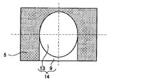
- FIG. 7 shows a planar configuration of the internal electrodes constituting the variable capacitance element according to Modification 1-2.
- the electrode body 13 of the internal electrode 14 has an elliptical shape.
- the major axis direction of the ellipse is configured as the minor axis direction of the dielectric layer 5
- the minor axis direction is configured as the major axis direction of the dielectric layer 5.
- the internal electrode 14 shown in FIG. 7 is laminated in two layers so that the sides and the center of the electrode body 13 overlap in the lamination direction, and the connection electrodes 9 face each other.
- the variable capacitance element body is configured so as to be exposed on the side surface. Then, by providing an external terminal that is electrically connected to each connection electrode 9 exposed at substantially the center in the major axis direction of the variable capacitor element body, the variable capacitor element of Modification 1-2 is formed.
- a capacitor is constituted by a pair of laminated electrode bodies 13.
- the electrode body 13 constituting the capacitor has an elliptical shape with high symmetry with respect to an axis that passes through the center of gravity of the electrode body 13 and is horizontal to the electrode surface. For this reason, the residual stress generated in the plane of the internal electrode 14 can be concentrated on the center, and the same effect as in this embodiment can be obtained.
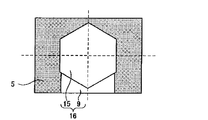
- FIG. 8 shows a planar configuration of the internal electrodes constituting the variable capacitance element according to Modification 1-3.
- the electrode body 15 of the internal electrode 16 has a regular hexagonal shape, and two vertices of the regular hexagonal shape overlap on a straight line in the minor axis direction passing through the center of the dielectric layer 5. It is configured as follows.
- the internal electrode 16 shown in FIG. 8 is laminated in two layers so that each side of the electrode body 15 and the center of gravity overlap in the lamination direction, and each connection electrode 9 is formed.
- the variable capacitance element body is configured so as to be exposed on the opposite side surfaces. Then, by providing an external terminal that is electrically connected to each connection electrode 9 exposed at substantially the center in the major axis direction of the variable capacitor element body, the variable capacitor element of Modification 1-3 is formed.
- a capacitor is constituted by a pair of stacked electrode bodies 15.
- the electrode body 15 constituting the capacitor is a regular hexagon having a high symmetry with respect to an axis that passes through the center of gravity of the electrode body 15 and is horizontal to the electrode surface. For this reason, the residual stress generated in the plane of the internal electrode 16 can be concentrated on the center, and the same effect as in this embodiment can be obtained.
- FIG. 9 shows a planar configuration of the internal electrodes constituting the variable capacitance element according to Modification 1-4.
- the electrode body 17 of the internal electrode 18 is a regular hexagon, and two vertices of the regular hexagon overlap each other on a straight line in the major axis direction passing through the center of the dielectric layer 5. It is configured as follows.
- the internal electrode 18 shown in FIG. 9 is laminated in two layers so that each side of the electrode body 17 and the center of gravity overlap each other in the laminating direction.
- the variable capacitance element body is configured so as to be exposed on the opposite side surfaces. Then, by providing an external terminal that is electrically connected to each connection electrode 9 exposed at substantially the center in the major axis direction of the variable capacitor element body, the variable capacitor element of Modification 1-4 is formed.
- a capacitor is constituted by a pair of stacked electrode bodies 17.
- the electrode body 17 constituting the capacitor is a regular hexagon having a high symmetry with respect to an axis that passes through the center of gravity of the electrode body 17 and is horizontal to the electrode surface. For this reason, the residual stress generated in the plane of the internal electrode 18 can be concentrated on the center, and the same effect as in this embodiment can be obtained.
- the shape of the electrode body is a regular hexagon.
- the regular polygon is a pentagon or more
- the same effect as the present embodiment can be obtained, and the shape of the electrode body is more circular. If the shape is close, a higher effect can be obtained.
- the generated residual stress can be further increased compared to the case where the electrode body is square. It can be concentrated on the center of gravity of the body.
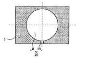
- FIG. 10 is a plan configuration diagram of the internal electrodes constituting the variable capacitance element according to the present embodiment. 10, parts corresponding to those in FIG. 2 are denoted by the same reference numerals, and redundant description is omitted.
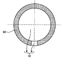
- the internal electrode 20 is connected to the circular electrode body 8 and the side of the electrode body 8, and is exposed to the side of the variable capacitor body to be external.
- the connection electrode 19 is connected to the terminal.
- the connection electrode 19 is formed in such a size that the residual stress generated around the connection electrode 19 during the sintering of the variable capacitance element body does not affect the residual stress generated in the electrode body 8 portion. . Accordingly, the area of the connection electrode 19 is formed to be sufficiently smaller than the area of the electrode body 8. In this embodiment, the width of the end connected to the external terminal of the connection electrode 19 is set to be larger than the diameter of the electrode body 8. It is formed small enough.
- the width of the end connected to the external terminal of the connection electrode 19 is, for example,
- the electrode body 8 is preferably set to a quarter or less of the diameter.
- the internal electrodes 20 shown in FIG. 10 are stacked so that the sides and the center of gravity of the electrode body 8 overlap in the stacking direction, and each of the stacked internal electrodes 20 is configured.
- the variable capacitance element body is configured such that the connection electrodes 19 are exposed on the opposite side surfaces. Then, by providing an external terminal that is electrically connected to each connection electrode 19 exposed at substantially the center in the major axis direction of the variable capacitance element body, the variable capacitance element of this embodiment is formed.
- a capacitor is constituted by a pair of stacked electrode bodies 8.
- the symmetry of the shape of the internal electrode 20 including the connection electrode 19 can be increased in a pseudo manner by reducing the width (area) of the connection electrode 19.
- the “symmetry” here means symmetry with respect to an axis that passes through the center of gravity of the electrode body 8 and is horizontal to the electrode surface, as in the first embodiment.
- FIG. 11 shows a planar configuration of the internal electrodes constituting the variable capacitance element according to Modification 2-1.
- the electrode body 21 of the internal electrode 22 is square.
- the area of the connection electrode 19 is sufficiently small compared to the area of the electrode body 21, and the width of the connection electrode 19 is sufficiently small compared to the square width. ing.
- the end of the connection electrode 19 connected to the external terminal The width is preferably set to be less than or equal to one-minute of the maximum width of the electrode body 21.
- the internal electrode 22 shown in FIG. 11 is laminated so that the side and the center of gravity of the electrode body 21 overlap in the laminating direction, and the connection electrodes 19 are formed on the side surfaces facing each other.
- the variable capacitance element body is configured so as to be exposed. Then, by providing an external terminal that is electrically connected to each connection electrode 19 exposed at substantially the center in the major axis direction of the variable capacitance element body, the variable capacitance element of this embodiment is formed.
- a capacitor is constituted by a pair of laminated electrode bodies 21.
- the symmetry of the internal electrode 22 can be artificially increased by reducing the area of the connection electrode 19. That is, the symmetry of the internal electrode 22 itself is higher than that of the comparative example 2 in which the width of the connection electrode is substantially the same as the width of the electrode body. For this reason, since the residual stress generated in the plane of the internal electrode 22 can be concentrated from each apex of the internal electrode 22 to the center, the same effect as the present embodiment can be obtained.
- the shape of the electrode body is circular and square, but the same effect can be obtained even when the shape is a regular polygon of pentagon or more, or an elliptical shape. . Even in that case, as long as the width of the connection electrode is formed to be sufficiently smaller than the width of the electrode body, the shape can pass through the center of gravity of the electrode body and can increase the symmetry with respect to the axis parallel to the electrode surface. Similar effects can be obtained.
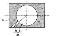
- FIG. 12 shows a planar configuration of the internal electrodes constituting the variable capacitance element according to Modification 2-2.
- the connection electrode 19 is formed so as to be exposed at substantially the center of the side surface in the major axis direction of the variable capacitance element body.
- the connection electrode 23 constituting the internal electrode 24 is formed so as to be exposed at a position off the center of the side surface in the major axis direction of the variable capacitance element body.
- connection electrode 23 constituting the internal electrode 24 is arranged on an axis passing through the center of gravity of the electrode body 8.
- the connection electrode 23 is arranged on an axis passing through the center of gravity of the electrode main body 8 constituting the capacitor, so that the symmetry of the residual stress can be reduced without much loss.
- the degree of freedom can be increased.
- the same effects as those of the first embodiment and the second embodiment can be obtained.
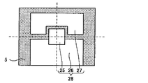
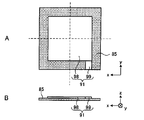
- FIG. 13 is a plan configuration diagram of the internal electrode 28 constituting the variable capacitance element of the present embodiment. In FIG. 13, parts corresponding to those in FIG.
- the internal electrode 28 is connected to the square electrode body 25 and the sides of the electrode body 25, and is exposed to the side of the variable capacitor element body.
- a connection electrode 26 connected to the terminal and a floating electrode 27 are included.
- the electrode body 25 is formed substantially at the center of the dielectric layer 5, and is formed so that the square center coincides with the center of the dielectric layer 5.
- the connection electrode 26 is connected to one side of the electrode body 25 and is formed so that the end is exposed on the side surface of the capacitor element body.
- the floating electrode 27 is formed in a region opposite to the connection electrode 26 across the electrode body 25.
- the floating electrode 27 has substantially the same shape as the connection electrode 26 and is formed so as to be substantially symmetric with respect to the connection electrode 26 with respect to an axis passing through the center of gravity of the electrode body 25.
- the floating electrode 27 is not connected to the electrode body 25 and is formed so as not to be exposed on the side surface of the variable capacitance element body. Therefore, no potential is supplied to the floating electrode 27 from the outside when the variable capacitance element is driven.
- the internal electrode 28 shown in FIG. 13 is laminated in two layers so that the sides and the center of gravity of the electrode body 25 overlap in the lamination direction, and the connection electrodes 26 face each other.
- the variable capacitance element body is configured so as to be exposed on the side surface. Then, by providing an external terminal that is electrically connected to each connection electrode 26 exposed at substantially the center in the major axis direction of the variable capacitor element body, the variable capacitor of this embodiment is formed.
- a capacitor is constituted by a pair of electrode bodies 25 that are stacked.
- the symmetry of the entire internal electrode can be enhanced by providing the floating electrode 27 so as to be symmetric with respect to the connection electrode 26 across the electrode body 25.
- the residual stress generated with the shrinkage at the time of baking can be concentrated on the center and can be made uniform in the plane.
- the electrical characteristics can be improved.
- the same effects as those of the first embodiment can be obtained.
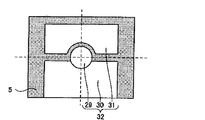
- FIG. 14 shows a planar configuration of the internal electrodes constituting the variable capacitance element according to Modification 3-1.
- the variable capacitance element according to Modification 3-1 is an example in which the shape of the electrode body 29 of the internal electrode 32 is different from that of the third embodiment.
- the internal electrode 32 includes a circular electrode body 29, a connection electrode 30 connected to the side of the electrode body 29, exposed on the side surface of the variable capacitance element body and connected to an external terminal, and a floating electrode 31. ing.
- the electrode body 29 is formed substantially at the center of the dielectric layer 5, and the center of gravity of the electrode body 29 is formed to coincide with the center of the dielectric layer 5.
- the connection electrode 30 is formed so as to be connected to one side of the electrode main body 29 and to be exposed at the side surface of the capacitive element main body.
- the floating electrode 31 is formed in a region opposite to the connection electrode 30 with the electrode body 29 interposed therebetween.
- the floating electrode 31 has substantially the same shape as the connection electrode 30 and is formed so as to be symmetric with respect to the connection electrode 30 with respect to an axis passing through the center of gravity of the electrode body 29.
- the floating electrode 31 is not connected to the electrode body 29 and is formed so as not to be exposed on the side surface of the variable capacitance element body. Therefore, no potential is supplied to the floating electrode 31 from the outside when the variable capacitance element is driven.
- the internal electrode 32 shown in FIG. 14 is laminated in two layers so that the sides and the center of gravity of the electrode body 29 overlap in the lamination direction, and the connection electrodes 30 face each other.
- the variable capacitance element body is configured so as to be exposed on the side surface. Then, by providing an external terminal that is electrically connected to each connection electrode 30 exposed on the side surface of the variable capacitance element body, the variable capacitance element of Modification 3-1 is formed.
- a capacitor is constituted by a pair of stacked electrode bodies 29.
- the floating electrode 31 is provided so as to be symmetric with respect to the connection electrode 30 with the electrode body 29 interposed therebetween. For this reason, the effect similar to 3rd Embodiment can be acquired. Furthermore, in Modification 3-1, since the electrode body 29 constituting the capacitor is circular, the residual stress generated in the surface can be concentrated more in the center.
- FIG. 15 shows a planar configuration of the internal electrodes constituting the variable capacitance element according to Modification 3-2.
- the internal electrode 35 includes a square electrode body 25, a connection electrode 33 connected to the side of the electrode body 25, exposed to the side surface of the variable capacitance element body, and connected to an external terminal; It consists of two floating electrodes 27 and 34.
- the connection electrode 33 is formed with a sufficiently narrow width compared to the width of the electrode body 25.
- the two floating electrodes 27 and 34 are formed in both regions sandwiching the connection electrode 33 and the electrode main body 25, and are formed symmetrically with respect to an axis passing through the center of gravity of the electrode main body 25.
- the internal electrode 35 shown in FIG. 15 is stacked in two layers so that the sides and the center of gravity of the electrode body 25 overlap in the stacking direction, and the connection electrodes 33 face each other.
- the variable capacitance element body is configured so as to be exposed on the side surface. Then, by providing an external terminal that is electrically connected to each connection electrode 33 exposed on the side surface of the variable capacitance element body, the variable capacitance element of Modification 3-2 is formed.
- a capacitor is constituted by a pair of stacked electrode bodies 25.
- connection electrode 33 since the width of the connection electrode 33 is formed to be ten parts smaller than the width of the electrode body 25, the residual stress generated in the connection electrode 33 portion can be reduced. Furthermore, in the modified example 3-2, the residual stress generated at the center of the capacitor can be increased by forming the floating electrodes 27 and 34 that do not form a capacitor symmetrically in both regions sandwiching the electrode body 25. . Therefore, the electrical characteristics of the variable capacitance element can be improved. In addition, the same effects as those of the third embodiment can be obtained.
- FIG. 16 shows a planar configuration of the internal electrodes constituting the variable capacitance element according to Modification 3-3.
- the internal electrode 38 includes a circular electrode body 29, a connection electrode 36 connected to the side of the electrode body 29, exposed to the side surface of the variable capacitance element body, and connected to an external terminal; It consists of two floating electrodes 31 and 37.
- the connection electrode 36 has a width that is sufficiently narrower than the diameter of the electrode body 29.
- the two floating electrodes 31 and 37 are formed in both regions sandwiching the connection electrode 36 and the electrode main body 29, and are formed symmetrically with respect to an axis passing through the center of gravity of the electrode main body 29.
- the internal electrode 38 shown in FIG. 16 is laminated in two layers so that the sides and the center of gravity of the electrode body 29 overlap in the lamination direction, and the connection electrodes 36 face each other.
- the variable capacitance element body is configured so as to be exposed on the side surface. Then, by providing an external terminal electrically connected to each connection electrode 36 exposed on the side surface of the variable capacitor element body, the variable capacitor element of Modification 3-3 is formed.
- a capacitor is constituted by the pair of electrode bodies 29 stacked.
- the width of the connection electrode 36 is formed to be ten parts smaller than the width of the electrode body 29, the residual stress generated in the connection electrode 36 can be reduced. Further, in the modified example 3-3, the residual stress generated at the center of the capacitor can be increased by forming the floating electrodes 31 and 37 that do not form a capacitor symmetrically in both regions sandwiching the electrode body 29. . Therefore, the electrical characteristics of the variable capacitance element can be improved. In addition, the same effects as those of the third embodiment can be obtained.
- variable capacitor according to the fourth embodiment of the present disclosure will be described.
- the shape of the variable capacitance element body is different from that of the first embodiment, and the shape and cross-sectional configuration of the internal electrode are the same as those of the variable capacitance element according to the first embodiment shown in the drawing. The illustration is omitted.
- FIG. 17 is an external perspective view of the variable capacitor according to this embodiment.
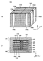
- variable capacitance element 40 of the present embodiment example includes a variable capacitance element body 41 and two external terminals 42 and 43.
- the variable capacitance element body 41 is configured as a rectangular parallelepiped (or a cube) whose planar shape parallel to the surface on which the internal electrodes are formed is a square shape. That is, in this embodiment, as shown in FIG. 17, the plane parallel to the surface on which the internal electrode is formed is a square shape having a lateral width W and a longitudinal width W.
- the surface on which the internal electrode is formed is a square shape, so that the symmetry of the shape of the variable capacitance element body 41 is enhanced. Residual stress generated during firing of the variable capacitance element body 41 is generated due to a difference in shrinkage rate (linear expansion coefficient) between the electrode material and the dielectric material. Therefore, the residual stress can be more concentrated toward the center by improving the symmetry of the internal electrodes and improving the symmetry of the outer shape of the variable capacitance element body 41. Thereby, the electrical characteristics of the capacitor formed by the internal electrodes can be improved. In addition, the same effects as those of the first embodiment can be obtained.
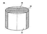
- FIG. 18 is an external perspective view of a variable capacitor according to Modification 4-1.
- Modification 4-1 is an example in which the shape of the variable capacitor element body is different from that of the first embodiment, and the shape and cross-sectional configuration of the internal electrode are the same as those of the variable capacitor according to the first embodiment shown in the drawing. Because of this, illustration is omitted.
- variable capacitance element 44 includes a variable capacitance element main body 45 and two external terminals 46 and 47.
- the variable capacitance element body 45 is formed in a cylindrical shape such that a planar shape parallel to the surface on which the internal electrode is formed is a circular shape.
- the outer shape of the variable capacitor element body 45 is formed in a cylindrical shape, so that the symmetry of the outer shape of the variable capacitor element body 45 with respect to the straight line in the stacking direction passing through the center of the electrode body of the internal electrode is enhanced. . Thereby, the residual stress which generate
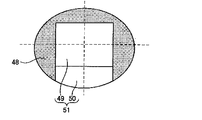
- FIG. 19 shows a planar configuration of a dielectric layer and internal electrodes that constitute a variable capacitance element according to Modification 4-2.
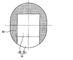
- the internal electrode 51 is formed so as to be connected to one side of the electrode body 49 having a square shape, and to be exposed on the side surface of the capacitance element body.
- the connection electrode 50 is formed.
- the planar shape in which the internal electrode 51 of the variable capacitance element body is formed that is, the planar shape of the dielectric layer 48 is an elliptical shape, and the connection electrode 50 constituting the internal electrode 51 is an elliptical dielectric layer. 48 are formed in the minor axis direction.
- the internal electrode 51 shown in FIG. 19 is laminated in two layers so that the sides of the electrode body 49 and the center of gravity overlap in the lamination direction, and the connection electrodes 50 face each other.
- the variable capacitance element body is configured so as to be exposed on the side surface. Then, by providing an external terminal that is electrically connected to each connection electrode 50 exposed on the side surface of the variable capacitance element body, the variable capacitance element of Modification 4-2 is formed.
- a capacitor is constituted by a pair of stacked electrode bodies 49.
- the outer shape of the variable capacitor element body is formed in a columnar shape having an elliptical cross section, so that the symmetry of the outer shape of the variable capacitor element body can be enhanced, which is the same as in the fourth embodiment. The effect of can be obtained.
- FIG. 20 shows a planar configuration of a dielectric layer and internal electrodes that constitute a variable capacitance element according to Modification 4-3.
- the internal electrode 51 is the same as that in Modification 4-2.
- the planar shape in which the internal electrode 51 of the variable capacitance element body is formed, that is, the dielectric layer 52 is elliptical, and the connection electrode 50 constituting the internal electrode 51 is the major axis of the elliptical dielectric layer 52. Is formed in the direction.
- the internal electrode 51 shown in FIG. 20 is stacked in two layers so that the sides and the center of gravity of the electrode body 49 overlap in the stacking direction, and the connection electrodes 50 face each other.
- the variable capacitance element body is configured so as to be exposed on the side surface. Then, by providing an external terminal that is electrically connected to each connection electrode 50 exposed on the side surface of the variable capacitor element body, the variable capacitor element of Modification 4-3 is formed.
- a capacitor is constituted by a pair of stacked electrode bodies 49.
- the outer shape of the variable capacitor element body is formed in a columnar shape having an elliptical cross section, so that the symmetry of the outer shape of the variable capacitor element body can be enhanced, and is the same as in the fourth embodiment. The effect of can be obtained.
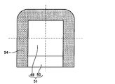
- FIG. 21 shows a planar configuration of a dielectric layer and internal electrodes that constitute a variable capacitance element according to Modification 4-4.
- the internal electrode 51 is the same as that of Modification 4-2.
- the planar shape in which the internal electrode 51 of the variable capacitance element body is formed that is, the dielectric layer 53 has a rounded rectangular shape (oval type), and the connection electrode 50 constituting the internal electrode 51 has a rounded rectangular shape.
- the dielectric layer 53 is formed in the major axis direction.
- the internal electrode 51 shown in FIG. 21 is laminated in two layers so that the sides of the electrode body 49 and the center of gravity overlap in the lamination direction, and the connection electrodes 50 face each other.
- the variable capacitance element body is configured so as to be exposed on the side surface. Then, by providing an external terminal that is electrically connected to each connection electrode 50 exposed on the side surface of the variable capacitor element body, the variable capacitor element of Modification 4-4 is formed.
- a capacitor is constituted by a pair of stacked electrode bodies 49.
- the outer shape of the variable capacitor element body is formed in a columnar shape having a cross-sectional oval shape, so that the symmetry of the outer shape of the variable capacitor element body can be increased, and is the same as in the fourth embodiment. The effect of can be obtained.
- FIG. 22 shows a planar configuration of a dielectric layer and internal electrodes that constitute a variable capacitance element according to Modification 4-5.
- the internal electrode 51 is the same as that of Modification 4-2.
- the planar shape in which the internal electrode of the variable capacitance element body is formed that is, the dielectric layer is formed in a quadrangular shape in which two corners positioned on both sides of one side of the square shape are rounded.
- the internal electrodes shown in FIG. 22 are stacked such that the sides and the center of gravity of the electrode body overlap in the stacking direction, and the respective connections constituting the stacked internal electrodes
- the variable capacitance element body is configured such that the electrodes are exposed on the opposite side surfaces. Then, by providing external terminals that are electrically connected to the respective connection electrodes exposed on the side surfaces of the variable capacitor element body, the variable capacitor element of Modification 4-5 is formed.
- the capacitor is configured by the stacked square electrode bodies.
- the outer shape of the variable capacitor element body is formed in a prismatic shape with one corner being rounded, thus improving the planar shape of the dielectric layer and the symmetry of the variable capacitor element body. And the same effects as in the fourth embodiment can be obtained.
- FIG. 23 shows a planar configuration of a dielectric layer and internal electrodes that constitute a variable capacitance element according to Modification 4-6.
- the internal electrode 51 is the same as that in Modification 4-2.
- the planar shape in which the internal electrode 51 of the variable capacitance element body is formed, that is, the dielectric layer 55 is formed in a rounded square shape in which four square corners are rounded.
- the internal electrode 51 shown in FIG. 23 is laminated in two layers so that the sides and the center of gravity of the electrode body 49 overlap in the lamination direction, and the connection electrodes 50 face each other.
- the variable capacitance element body is configured so as to be exposed on the side surface. Then, by providing an external terminal that is electrically connected to each connection electrode 50 exposed on the side surface of the variable capacitor element body, the variable capacitor element of Modification 4-6 is formed.
- a capacitor is constituted by a pair of stacked electrode bodies 49.
- the outer shape of the variable capacitor element body is formed in a columnar shape with a rounded square cross section, so that the symmetry of the variable capacitor element body can be increased, and the fourth embodiment and Similar effects can be obtained.
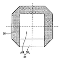
- FIG. 24 shows a planar configuration of a dielectric layer and internal electrodes constituting a variable capacitance element according to Modification 4-7.
- the internal electrode 51 is the same as that of Modification 4-2.
- the planar shape on which the internal electrode 51 of the variable capacitance element body is formed, that is, the dielectric layer 56 is formed in an octagonal shape.
- the internal electrode 51 shown in FIG. 24 is stacked in two layers so that the sides and the center of gravity of the electrode body overlap in the stacking direction, and the connection electrodes 50 face each other.
- the variable capacitance element body is configured so as to be exposed on the side surface. Then, by providing an external terminal that is electrically connected to each connection electrode 50 exposed on the side surface of the variable capacitor element body, the variable capacitor element of Modification 4-7 is formed.
- a capacitor is constituted by a pair of stacked electrode bodies 49.
- the outer shape of the variable capacitor element body is formed in a columnar shape having an octagonal cross section, so that the symmetry of the outer shape of the variable capacitor element body can be improved, and the same as in the fourth embodiment The effect of can be obtained.
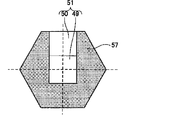
- FIG. 25 shows a planar configuration of a dielectric layer and internal electrodes that constitute a variable capacitance element according to Modification 4-8.
- the internal electrode 51 is the same as that in Modification 4-2.
- the planar shape on which the internal electrode 51 of the variable capacitance element body is formed, that is, the dielectric layer 57 is formed in a regular hexagonal shape.
- the internal electrode 51 shown in FIG. 25 is laminated in two layers so that the sides and the center of gravity of the electrode body 49 overlap in the lamination direction, and the connection electrodes 50 face each other.
- the variable capacitance element body is configured so as to be exposed on the side surface. Then, by providing an external terminal that is electrically connected to each connection electrode 50 exposed on the side surface of the variable capacitor element body, the variable capacitor element of Modification 4-8 is formed.
- a capacitor is configured by the pair of electrode bodies 49 stacked.
- the outer shape of the variable capacitor element body is formed in a columnar shape having a regular hexagonal cross section, so that the symmetry of the outer shape of the variable capacitor element body can be improved. Similar effects can be obtained.
- FIG. 26 is a plan configuration diagram of a dielectric layer and internal electrodes constituting the variable capacitance element of the present embodiment.
- the outer shape of the variable capacitance element body is an example different from that of the first embodiment.
- the internal electrode 10 is formed so as to be connected to one side of the electrode body 8 having a circular shape and the electrode body 8 so that the end portion is exposed on the side surface of the capacitance element body.
- connection electrode 9 The planar shape on which the internal electrode 10 of the variable capacitance element body is formed, that is, the dielectric layer 58 is formed in a circular shape.
- the center of gravity of the electrode body 8 of the internal electrode 10 is formed so as to be positioned at the center of the dielectric layer 58.
- the internal electrode 10 shown in FIG. 26 is laminated in two layers so that the sides and the center of gravity of the electrode body 8 overlap in the lamination direction, and the connection electrodes 9 face each other.
- the variable capacitance element body is configured so as to be exposed on the side surface. Then, by providing an external terminal that is electrically connected to each connection electrode 9 exposed on the side surface of the variable capacitance element body, the variable capacitance element of this embodiment is formed.
- a capacitor is constituted by a pair of stacked electrode bodies 8.
- the shape of the electrode body 8 constituting the capacitance of the internal electrode 10 and the planar shape of the dielectric layer 58 are the same, the symmetry of the outer shape of the electrode body 8 and the variable capacitance element body is the same. Is increased. Thereby, the residual stress generated at the time of firing the variable capacitance element body can be concentrated in the central direction, and the electrical characteristics of the capacitor constituted by the pair of electrode bodies 8 can be improved. In addition, the same effects as those of the first embodiment can be obtained.
- FIG. 27 shows a planar configuration of a dielectric layer and internal electrodes constituting a variable capacitance element according to Modification 5-1.
- the internal electrode 20 has the same configuration as the internal electrode 20 of the second embodiment.
- the internal electrode shown in FIG. 27 is laminated in two layers so that the side and the center of gravity of the electrode body 8 overlap in the lamination direction, and the connection electrodes 19 face each other.
- the variable capacitance element body is configured so as to be exposed on the side surface. Then, by providing an external terminal electrically connected to each connection electrode 19 exposed on the side surface of the variable capacitor element body, the variable capacitor element of Modification 5-1 is formed.
- a capacitor is constituted by a pair of stacked electrode bodies 8.
- the area of the connection electrode 19 connected to the electrode body 8 in the internal electrode 20 is sufficiently smaller than that of the electrode body 8. For this reason, the shape of the dielectric layer 58 and the internal electrode 20 can be brought closer to a similar relationship.
- FIG. 28 is a plan view of the two internal electrodes 20 of the variable capacitor according to Modification 5-1 as seen through the top surface.
- the residual stress generated in the lower internal electrode 20 is indicated by an arrow e
- the residual stress generated in the upper internal electrode 20 is indicated by an arrow f.
- the connection electrode 19 is formed sufficiently smaller than the area of the electrode body 8, the contribution to the residual stress in the connection electrode 19 portion is reduced. For this reason, compared with the internal electrode 10 according to the first embodiment in which the width of the connection electrode 9 is formed to be substantially the same as the diameter of the electrode body 8, the residual stress generated toward the center of the electrode body 8 is entirely present. Will be equal. As a result, the tensile stress in the stacking direction (electric field direction) of the internal electrode 20 is further increased, and the electrical characteristics of the capacitor are improved.
- the shape of the electrode body 8 constituting the capacitance of the internal electrode 20 and the planar shape of the dielectric layer 58 are the same shape, the outer shape of the electrode body 8 and the variable capacitance element body. And the same effects as those of the fifth embodiment can be obtained.
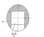
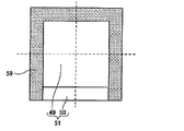
- FIG. 29 shows a planar configuration of a dielectric layer and internal electrodes that constitute a variable capacitance element according to Modification 5-2.
- the internal electrode 51 includes a square electrode body 49 and a connection electrode formed so as to be connected to one side of the electrode body 49 and to be exposed at the side surface of the capacitive element body. And 50.
- the planar shape in which the internal electrode 51 of the variable capacitance element body is formed that is, the planar shape of the dielectric layer 59 is a square shape.
- the center of gravity of the electrode body 49 of the internal electrode 51 is formed so as to be positioned at the center of the dielectric layer 59.
- the internal electrode 51 shown in FIG. 29 is laminated in two layers so that the side of the electrode body 49 and the center of gravity overlap in the laminating direction, and the connection electrodes 50 face each other.
- the variable capacitance element body is configured so as to be exposed on the side surface. Then, by providing an external terminal that is electrically connected to each connection electrode exposed on the side surface of the variable capacitance element body, the variable capacitance element of Modification 5-2 is formed.
- a capacitor is constituted by the pair of electrode bodies 49 stacked.
- the shape of the electrode body 49 constituting the capacitance of the internal electrode 51 and the dielectric layer 5 Since the planar shape of 9 is the same shape, the symmetry of the outer shape of the electrode main body 49 and the variable capacitance element main body is enhanced, and the same effect as in the fifth embodiment can be obtained.
- FIG. 30 shows a planar configuration of a dielectric layer and internal electrodes that constitute a variable capacitance element according to Modification 5-3.
- the internal electrode 22 has the same configuration as the internal electrode 22 of Modification 2-1 shown in FIG.
- the internal electrode 22 shown in FIG. 30 is stacked in two layers so that the sides and the center of gravity of the electrode body 21 overlap in the stacking direction, and the connection electrodes 19 face each other.
- the variable capacitance element body is configured so as to be exposed on the side surface. Then, by providing an external terminal that is electrically connected to each connection electrode 19 exposed on the side surface of the variable capacitor element body, the variable capacitor element of Modification 5-3 is formed.
- a capacitor is configured by the stacked circular electrode bodies.
- the area of the connection electrode 19 connected to the electrode body 21 in the internal electrode 22 is formed sufficiently smaller than that of the electrode body 21. For this reason, the shape of the dielectric layer 59 and the internal electrode 22 can be brought closer to a similar relationship. Thereby, the residual stress generated at the time of firing the variable capacitance element body can be concentrated more toward the center, and the electrical characteristics of the capacitor can be improved. In addition, the same effects as those of the fifth embodiment can be obtained.
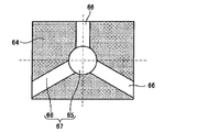
- FIG. 31 is a perspective view of a variable capacitor according to this embodiment.
- FIG. 32 is a plan configuration diagram of internal electrodes constituting the variable capacitance element according to the present embodiment.
- variable capacitance element includes a variable capacitance element main body 62 formed of a rectangular parallelepiped member and three external terminals 63a and 63b formed respectively.
- the external terminals 63a and 63b are provided apart from each other on the side surface of the variable capacitance element body.
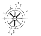
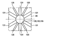
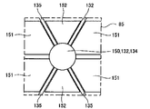
- the variable capacitance element main body 62 has a configuration in which two internal electrodes 67 shown in FIG.
- the internal electrode 67 includes a circular electrode body 65 and three connections that are connected to the electrode body 65 and formed at equal intervals in the circumferential direction of the electrode body 65.
- An electrode 66 is included.
- the dielectric layer 64 has a rectangular plane on which the internal electrodes 67 are formed.
- connection electrodes 66 are each formed in a strip shape that is thinner than the diameter of the electrode body 65 and are exposed on the side surface of the variable capacitor element body 62. Further, when the internal electrode 67 shown in FIG. 32 and the internal electrode 67 in a state where the internal electrode 67 shown in FIG. 32 is rotated 180 degrees about the axis perpendicular to the electrode surface are stacked, the connection electrode 66 is stacked in the stacking direction. It is formed so as not to overlap.
- variable capacitance element is formed by stacking the internal electrode 67 shown in FIG. 32 and the internal electrode 67 in a state where the internal electrode 67 shown in FIG. 32 is rotated 180 degrees about an axis perpendicular to the electrode surface.
- the body can be configured.
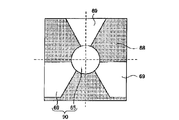
- FIG. 33 is a view of the variable capacitor element body 62 of this embodiment as seen through the top surface.
- connection electrodes 66 formed on the two stacked internal electrodes 32 do not overlap each other in the stacking direction. For this reason, in this embodiment, no capacitor is formed between the connection electrodes 66 to be stacked, and a capacitor is constituted by the electrode body 65 overlapping in the stacking direction. Then, by providing the external terminals 63a and 63b connected to the six connection electrodes 66 exposed on the side surface of the variable capacitor element body 62 of the present embodiment example, the variable capacitor element 61 of the present embodiment example is formed. .
- the withstand voltage against the input signal voltage can be improved by increasing the number of connection electrodes 66 connected to one electrode body 65.
- the electrode body 65 forming the capacitor is formed in a circular shape, and the connection electrodes 66 connected to the electrode body 65 are formed in three equally spaced directions, whereby the symmetry of the internal electrode 67 is achieved. Can be increased. Thereby, the residual stress generated during firing of the variable capacitance element body 62 can be concentrated toward the center, and the electrical characteristics of the capacitor can be improved. In addition, the same effects as those of the first embodiment can be obtained.
- FIG. 34 shows a planar configuration of a dielectric layer and internal electrodes that constitute a variable capacitance element according to Modification 6-1.
- the internal electrode 70 includes a circular electrode body 65 and three connection electrodes 69 connected to the electrode body 65 and formed at equal intervals in the circumferential direction of the electrode body 65. ing.
- the dielectric layer 68 has a square surface on which the internal electrode 70 is formed.
- connection electrodes 69 are formed to be wide from the side connected to the electrode main body 65 to the end side exposed on the side surface of the variable capacitance element main body. Further, when the internal electrode 70 shown in FIG. 34 and the internal electrode 70 shown in FIG. 34 rotated by 180 degrees about an axis perpendicular to the electrode surface are stacked, the connection electrode 69 is stacked in the stacking direction. Form so as not to overlap.
- the internal electrode 70 shown in FIG. 34 and the internal electrode 70 shown in FIG. 34 are laminated by laminating the internal electrode 70 in a state where the internal electrode 70 is rotated 180 degrees about an axis perpendicular to the electrode surface.
- a capacitive element body can be configured. By doing so, a total of six connection electrodes 69 formed on the two stacked internal electrodes 70 are exposed on the side surfaces that do not overlap in the stacking direction. Further, since the connection electrodes 69 formed in the stacking direction do not overlap in the stacking direction, no capacitance is formed between the stacked connection electrodes 69. Then, by providing external terminals connected to the six connection electrodes 69 exposed on the side surface of the variable capacitor element body, the variable capacitor element of Modification 6-1 is formed.
- connection electrode 69 is formed wider toward the side connected to the external terminal. Therefore, the breakdown voltage can be further improved as compared with the variable capacitance element 61 according to the sixth embodiment. In addition, the same effects as those of the sixth embodiment can be obtained.
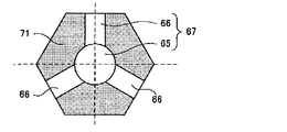
- FIG. 35 shows a planar configuration of a dielectric layer and internal electrodes that constitute a variable capacitance element according to Modification 6-2.
- portions corresponding to those in FIG. Modification 6-2 is an example in which the planar shape of the dielectric layer is different from that of the sixth embodiment.
- the planar shape of the dielectric layer 71 is a regular hexagon.
- the three connection electrodes 66 are formed so as to be exposed on every other side surface of the regular hexagonal dielectric layer 71.
- the internal electrode 67 shown in FIG. 35 and the internal electrode 67 in a state in which the internal electrode 67 shown in FIG. 35 is rotated by 180 degrees about an axis perpendicular to the electrode surface are laminated.
- the variable capacitance element body can be configured.
- the variable capacitance element according to the modification example 6-2 is formed.
- the variable capacitance element body has a regular hexagonal cross section and is formed in a columnar shape.
- variable capacitance element according to Modification 6-2, the outer shapes of the internal electrode 67 and the variable capacitance element body are highly symmetrical, and the residual stress generated during firing of the variable capacitance element body can be further increased. The same effect as that of the sixth embodiment can be obtained.
- variable capacitance elements In the variable capacitance elements according to the first to sixth embodiments described above and the variable capacitance elements according to the modifications, the laminated internal electrodes have been described as having the same shape. However, the present disclosure is not limited to this, and an effect of improving electrical characteristics due to an increase in residual stress can be obtained even when internal electrodes having different shapes are stacked in combination. When the electrode bodies of the stacked internal electrodes have the same shape as in the first to sixth embodiments described above, the electrical characteristics can be further improved.
- variable capacitance element obtained by combining and stacking internal electrodes having different shapes
- a variable capacitance element including a plurality of capacitors connected in series in the stacking direction of internal electrodes will be described as an example.
- FIG. 36A is a schematic perspective view of a variable capacitance element 81 according to the seventh embodiment of the present disclosure
- FIG. 36B is a cross-sectional configuration diagram of the variable capacitance element 81.
- the stacking direction of internal electrodes which will be described later, is the z direction
- one direction of the variable capacitor 81 that is orthogonal to the stack direction is the x direction
- the other direction of the variable capacitor 81 is
- one surface constituted by the xy plane of the variable capacitance element 81 will be described as an “upper surface” and the other surface constituted by the xy plane will be described as a “lower surface”.
- the surfaces perpendicular to the upper surface and the lower surface of the variable capacitance element 1 are “side surfaces”.
- variable capacitance element 1 includes a variable capacitance element main body 82 formed of a rectangular parallelepiped member having an xy plane that is square and six external terminals (hereinafter, first external terminals 83a respectively). To sixth external terminal 83f).
- the first external terminal 83a is formed on one side surface constituted by the yz surface of the variable capacitance element main body 82
- the sixth external terminal 83f is formed on the other side surface constituted by the yz surface of the variable capacitance element main body 82.
- the second external terminal 83b and the fourth external terminal 83d are formed to be separated from each other on one side formed by the xz plane of the variable capacitance element body 82, and the third external terminal 83c and the fifth external terminal 83e are variable.
- the capacitor element main body 82 is formed on the other side surface constituted by the xz plane so as to be separated from each other.
- the second external terminal 83b and the third external terminal 83c are positioned diagonally, and the fourth external terminal 83d and the fifth external terminal 83e are positioned diagonally.
- the first external terminal 83a to the sixth external terminal 83f are formed so as to cover the side surface of the variable capacitance element body 82 in the z direction and to protrude from the upper surface and the lower surface of the variable capacitance element body 82, respectively.
- the variable capacitance element main body 82 includes a dielectric layer 85 and six internal electrodes 88 to 93 stacked via the dielectric layer 85.
- the six internal electrodes will be described as the first internal electrode 88 to the sixth internal electrode 93, respectively.
- the variable capacitor element body 82 of the present embodiment is configured such that the first internal electrode 88 to the sixth internal electrode 93 are laminated in this order from the lower surface to the upper surface.
- the lower dielectric layer 86 is laminated below the first internal electrode 88, and the upper dielectric layer 87 is laminated above the sixth internal electrode 93.
- FIG. 37 is an exploded view of the variable capacitor element body 82 when viewed from one side surface in the long side direction.
- FIG. 38A is a plan configuration diagram when the first internal electrode 88 is viewed from above, and FIG. 38B is a configuration diagram when the first internal electrode 88 is viewed from one side surface.
- FIG. 39A is a plan configuration diagram when the second internal electrode 89 is viewed from above, and FIG. 39B is a configuration diagram when the second internal electrode 89 is viewed from one side surface.
- 40A is a plan configuration diagram when the fourth internal electrode 91 is viewed from the top surface, and FIG. 40B is a configuration diagram when the fourth internal electrode 91 is viewed from one side surface.
- a line passing through the dielectric layer 85 and the center (center of gravity) of each internal electrode is indicated by a broken line.
- the variable capacitor element body 2 has a structure in which a sheet-like dielectric layer 85 having an internal electrode formed on one surface is laminated.
- Each dielectric layer 85 formed in a sheet shape has a square planar shape.
- each dielectric layer 85 is laminated so that the side on which the internal electrode is formed faces the upper surface. Yes.
- a plurality of dielectric layers 85 on which no electrodes are formed are provided on the lower layer of the first internal electrode 88 and the upper layer of the sixth internal electrode 93.
- This dielectric layer 85 constitutes a lower dielectric layer 86 and an upper dielectric layer 87.
- the lower dielectric layer 86 and the upper dielectric layer 87 constituted by the plurality of dielectric layers 85 can prevent the electrodes from being exposed on the upper surface and the lower surface of the variable capacitance element body 82.
- the dielectric layer 85 is made of a ferroelectric material in order to constitute the variable capacitance element 1 whose capacitance changes according to the applied voltage. Also in this embodiment, the same ferroelectric material as that in the first embodiment can be used.
- the first internal electrode 88 includes an electrode body 94 and a connection electrode 95 as shown in FIGS. 38A and 38B.
- the electrode body 94 has a square shape in plan view, and is smaller than the area of the dielectric layer 85 formed in a sheet shape, that is, the area of the xy plane of the variable capacitor element body 82 and is exposed on the side surface of the variable capacitor element body 82. It is formed so as not to.
- the electrode body 94 is formed such that the center of gravity thereof coincides with the center of the dielectric layer 85.
- connection electrode 95 is formed so as to be connected to one side of the electrode main body 94 extending in the y direction and to be exposed on the side surface of the variable capacitance element main body 82.
- the width of the connection electrode 95 in the x direction is the same as the width of the electrode body 94 in the x direction.
- the end portion of the connection electrode 95 exposed on the side surface of the variable capacitance element body 82 is electrically connected to the first external terminal 83a.
- the second internal electrode 89 includes an electrode body 96 and a connection electrode 97 as shown in FIGS. 39A and 39B.
- the electrode main body 96 has the same size and the same shape as the electrode main body 94 constituting the first internal electrode 88 and is formed so that the center thereof coincides with the center of the dielectric layer 85.
- connection electrode 97 is formed so as to be connected to the side extending in the x direction of the electrode main body 96 and is formed so as to be exposed on the side surface of the variable capacitance element main body 82. Further, the width of the connection electrode 97 in the y direction is sufficiently smaller than the width of the electrode body 96 in the y direction, and is formed so as to be connected to one end of the side of the electrode body 96 in the y direction. . The end portion of the connection electrode 97 exposed on the side surface of the variable capacitance element body 82 is electrically connected to the second external terminal 83b.
- the 4th internal electrode 91 is comprised by the electrode main body 98 and the connection electrode 99, as shown to FIG. 40A and 40B.
- the electrode main body 98 has the same size and the same shape as the electrode main body 94 constituting the first internal electrode 88, and is formed so that its center of gravity coincides with the center of the dielectric layer 85.
- connection electrode 99 is formed so as to be connected to the side extending in the y direction of the electrode main body 98 and is formed so as to be exposed on the side surface of the variable capacitance element main body 82.
- the width of the connection electrode 99 in the y direction is sufficiently smaller than the width of the electrode body 98 in the y direction, and is spaced apart from the connection electrode 97 of the second internal electrode 89 when viewed in the xy plane.
- the electrode body 98 is formed so as to be connected to the other end of the side in the y direction.
- the end portion of the connection electrode 99 exposed on the side surface of the variable capacitance element body 82 is electrically connected to the fourth external terminal 83d.
- the third internal electrode 90 has a configuration in which the second internal electrode 89 shown in FIG. 39A is rotated by 180 degrees about an axis perpendicular to the electrode surface. 97. Accordingly, the connection electrode 97 of the third internal electrode 90 is formed at a position diagonal to the connection electrode 97 of the second internal electrode 89 when viewed in the xy plane. The connection electrode 97 of the third internal electrode 90 exposed on the side surface of the variable capacitance element body 82 is electrically connected to the third external terminal 83c.
- the fifth internal electrode 92 has a configuration in which the fourth internal electrode 91 shown in FIG. 40A is rotated 180 degrees around an axis perpendicular to the electrode surface, and the same electrode body 98 and connection electrode as the fourth internal electrode 91 99. Therefore, the connection electrode 99 of the fifth internal electrode 92 is formed at a position diagonal to the connection electrode 99 of the fourth internal electrode 91 when viewed in the xy plane.
- the connection electrode 99 of the fifth internal electrode 92 exposed on the side surface of the variable capacitance element body 82 is electrically connected to the fifth external terminal 83e.
- the sixth internal electrode 93 has a configuration in which the first internal electrode 88 shown in FIG. 38A is rotated 180 degrees about an axis perpendicular to the electrode surface, and the same electrode body 94 and connection electrode as the first internal electrode 88 are formed. 95. Therefore, the connection electrode 95 of the sixth internal electrode 93 is formed at a position facing the connection electrode 95 of the first internal electrode 88 when viewed in the xy plane.
- the connection electrode 95 of the sixth internal electrode 93 exposed on the side surface of the variable capacitance element body 82 is electrically connected to the sixth external terminal 83f.
- the first internal electrode 88 to the sixth internal electrode 93 of the present embodiment example can be formed using the same material as in the first embodiment.
- variable capacitance element 81 of the present embodiment example can also be formed by the same manufacturing process as that of the first embodiment. That is, the variable capacitance element body 82 is formed by laminating and firing the dielectric sheets on which the internal electrodes are formed so that the electrode formation surface is the upper surface, and forming the external terminals at desired positions on the side surfaces. Thus, the variable capacitance element 81 of the present embodiment example is manufactured. In the variable capacitance element 81 of this embodiment, the first internal electrode 88 and the sixth internal electrode 93, the second internal electrode 89 and the third internal electrode 90, the fourth internal electrode 91 and the fifth internal electrode 92 are provided. Since they have the same shape, they can be formed with the same mask.
- FIG. 41 shows a circuit configuration of the voltage control circuit.
- a voltage control circuit 200 shown in FIG. 41 is provided, for example, between an AC power supply 201 and a circuit such as a rectifier circuit, and receives an AC voltage (input signal) input from the AC power supply 201 to a circuit such as a rectifier circuit. Adjust to voltage value.
- the first external terminal 83a to the sixth external terminal 83f in FIG. 41 correspond to the first external terminal 83a to the sixth external terminal 83f in FIG.
- the laminated first internal electrode 88 to sixth internal electrode 93 are connected to different external terminals (first external terminal 83a to sixth external terminal 83f), respectively. Therefore, the first capacitor C ⁇ b> 1 is formed between the first internal electrode 88 and the second internal electrode 89.
- a second capacitor C ⁇ b> 2 is formed between the second internal electrode 89 and the third internal electrode 90.
- a third capacitor C3 is formed between the third internal electrode 90 and the fourth internal electrode 91.
- a fourth capacitor C4 is formed between the fourth internal electrode 91 and the fifth internal electrode 92.
- a fifth capacitor C ⁇ b> 5 is formed between the fifth internal electrode 92 and the sixth internal electrode 93.
- the variable capacitance element 81 of this embodiment is a circuit in which the first capacitor C1 to the fifth capacitor C5 are connected in series in this order.
- the second capacitor C2, the third capacitor C3, and the fourth capacitor C4 are used as variable capacitors, and the first capacitor C1 and the fifth capacitor C5 are used as DC removing capacitors. Therefore, the first external terminal 83 a of the variable capacitance element 81 is connected to one output terminal of the AC power supply 201, and the sixth external terminal 83 f is connected to the other output terminal of the AC power supply 201. That is, the series circuit including the first capacitor C1 to the fifth capacitor C5 is connected in parallel to the AC power supply 201.
- a circuit such as a rectifier circuit to which a signal from the AC power supply 201 is input is connected in parallel between the first external terminal 83a and the sixth external terminal 83f of the variable capacitance element 81.
- the second external terminal 83b and the fourth external terminal 83d are connected to the negative terminal of the control power source 202 via the DC removal resistors 203 and 205, respectively.
- the third external terminal 83c and the fifth external terminal 83e are connected to the positive terminal of the control power source 202 via the DC removal resistors 204 and 206, respectively. That is, in the variable capacitance element 81 of the present embodiment example, the control power source 202 is connected in parallel to the second capacitor C2, the third capacitor C3, and the fourth capacitor C4. The capacities of the second capacitor C2, the third capacitor C3, and the fourth capacitor C4 are adjusted by a DC signal (control signal) input from the control power source 202.
- the first capacitor C1 and the fifth capacitor C5 used as the DC removal capacitor and the three DC removal resistors are affected by interference between the DC bias current flowing from the control power source 202 and the AC current from the AC power source 201.
- an inductance (coil) for removing DC may be used instead of the resistor for removing DC.
- the shape of the internal electrode constituting each capacitor and the shape of the dielectric layer with respect to the internal electrode are highly symmetric. Therefore, the electrical characteristics can be improved, such as improvement of the capacitance variable rate of the variable capacitance element 81 and improvement of the capacitance.
- Modification 7-1 Next, a variable capacitor according to Modification 7-1 will be described.
- the external configuration, the cross-sectional configuration, and the circuit configuration are the same as those in FIGS. 36A, 36B, and 41 shown in the seventh embodiment. Duplicate explanation is omitted.
- FIG. 42 is an exploded view of the variable capacitance element main body 110 of the variable capacitance element according to Modification 7-1 when viewed from one side surface in the long side direction.
- the modified example 7-1 is an example in which the fourth internal electrode 91 and the fifth internal electrode 92 are formed using a mask used when the second internal electrode 89 and the third internal electrode 90 are manufactured.
- parts corresponding to those in FIG. 42 parts corresponding to those in FIG.
- the fourth internal electrode 91 passes through the second internal electrode 89 shown in FIG. 39A through the center of gravity of the electrode body 96 and is 180 degrees about the axis in the x direction horizontal to the plane of the electrode body 96.
- the configuration is rotated.
- the second internal electrode 89 shown in FIG. 39A is turned upside down around the x-direction axis. Therefore, the connection electrode 97 of the fourth internal electrode 91 is disposed apart from the connection electrode 97 of the second internal electrode 89 when viewed in the xy plane.
- the fourth external terminal 83 d is connected to the connection electrode 97 of the fourth internal electrode 91.
- the fifth internal electrode 92 rotates the second internal electrode 89 shown in FIG. 39A by 180 degrees about the y-direction axis passing through the center of gravity of the electrode body 96, and in the x direction passing through the center of gravity of the electrode body 96. It is the structure rotated 180 degree
- the second internal electrode 89 to the fourth internal electrode 91 are formed using the same mask, and the sheet-like dielectric layer on which each internal electrode is formed is stacked while being rotated and / or turned over.
- the variable capacitance element 81 similar to that in FIG. 36 can be formed.
- the first internal electrode 88 to the third internal electrode 90 are laminated so that their electrode surfaces face the upper surface
- the fourth internal electrode 91 to the sixth internal electrode 93 are Lamination is performed so that the electrode surface faces the lower surface.
- a dielectric layer 85 is formed between the third internal electrode 90 and the fourth internal electrode 91.
- connection electrodes 97 are exposed at different positions on the side surface of the variable capacitor element body. Can be configured to. Then, by connecting the respective external terminals to these connection electrodes 97, different potentials can be supplied to the respective internal electrodes, and they are connected in series in the stacking direction of the internal electrodes as in the seventh embodiment. Capacitors can be configured.
- the second internal electrode 89 to the fifth internal electrode 92 can be formed using the same mask, so that the cost can be reduced.
- the same effects as those of the seventh embodiment are obtained.
- Modification 7-2 Next, a variable capacitor according to Modification 7-2 will be described.
- the variable capacitance element of the modified example 7-2 has the same external configuration, cross-sectional configuration, and circuit configuration as those in FIGS. 36A, 36B, and 41 shown in the seventh embodiment. Duplicate explanation is omitted.
- FIG. 43 is an exploded view of the variable capacitor element body 111 of the variable capacitor according to Modification 7-2 as viewed from one side surface in the long side direction.
- the modified example 7-2 is an example in which the stress control units 100 and 101 are provided in the lower layer of the first internal electrode 88 and the upper layer of the sixth internal electrode 93.
- parts corresponding to those in FIG. 43 are provided in the lower layer of the first internal electrode 88 and the upper layer of the sixth internal electrode 93.
- the first stress control unit 100 is formed in the lower layer of the first internal electrode 88, and the second stress control unit 101 is formed in the upper layer of the sixth internal electrode 93. ing.
- the first stress control unit 100 includes a plurality of first internal electrodes 88 stacked via a dielectric layer 85, and the first internal electrode 88 that configures the first stress control unit 100 configures a first capacitor C1.
- the first external terminal 83a is connected to the first internal electrode 88. Accordingly, since the first internal electrode 88 constituting the first capacitor C1 and the first internal electrode 88 constituting the first stress control unit 100 are set to the same potential, no capacitor is formed between the electrodes. Furthermore, since the plurality of first internal electrodes 88 formed in the first stress control unit 100 are also at the same potential, no capacitor is formed in the first stress control unit 100.
- the second stress control unit 101 includes a plurality of sixth internal electrodes 93 stacked via a dielectric layer 85, and the sixth internal electrode 93 included in the second stress control unit 101 includes a fifth capacitor C5.
- the sixth internal electrode 93 is connected to the sixth external terminal 83f in the same manner as the sixth internal electrode 93. Therefore, since the sixth internal electrode 93 constituting the fifth capacitor C5 and the sixth internal electrode 93 constituting the second stress control unit 101 are set to the same potential, no capacitor is formed between the electrodes. Furthermore, since the plurality of sixth internal electrodes 93 formed in the second stress control unit 101 are also at the same potential, no capacitor is formed in the second stress control unit 101.
- variable capacitance element of Modification Example 7-2 residual stress is also generated in the first stress control unit 100 and the second stress control unit 101 due to the difference in shrinkage rate when the electrode material and the dielectric material are fired. . Therefore, since the residual stress increases by the first stress control unit 100 and the second stress control unit 101, it is possible to increase the capacitance value and increase the capacity variable rate compared to the case where the stress control unit is not formed. it can. In addition, the same effects as those of the seventh embodiment can be obtained.
- FIG. 44A is a schematic perspective view of a variable capacitance element 121 according to the eighth embodiment of the present disclosure
- FIG. 44B is a cross-sectional configuration diagram of the variable capacitance element 121.
- 44A and 44B parts corresponding to those in FIGS. 36A and 36B are denoted by the same reference numerals, and redundant description is omitted.
- variable capacitance element 121 of this embodiment includes a variable capacitance element main body 122 composed of a rectangular parallelepiped member whose xy plane is a square and 10 external terminals (hereinafter referred to as first external terminals respectively). 129a to 10th external terminal 129j).
- the first external terminal 129a to the tenth external terminal 129j are arranged on the four side surfaces of the variable capacitance element body 122 so as to be separated from each other.
- the first external terminal 129a and the eighth external terminal 129h, the second external terminal 129b and the third external terminal 129c, and the ninth external terminal 129i and the tenth external terminal 129j face each other when viewed in the xy plane. Placed in position.
- the fourth external terminal 129d and the seventh external terminal 129g, and the fifth external terminal 129e and the sixth external terminal f are disposed at positions facing each other when viewed in the xy plane.
- the first external terminal 129a to the tenth external terminal 129j are formed so as to cover the side surface of the variable capacitor element body 122 in the z direction and to protrude from the upper surface and the lower surface of the variable capacitor element body 122, respectively.
- variable capacitance element body 122 includes a dielectric layer 85 and six internal electrodes 123 to 128 stacked via the dielectric layer 85. As shown in FIG. In the following description, for convenience, the three internal electrodes will be described as the first internal electrode 123 to the sixth internal electrode 128, respectively.
- the variable capacitance element main body 122 of the present embodiment is configured such that the first internal electrode 123 to the sixth internal electrode 128 are laminated in this order from the lower surface to the upper surface.
- FIG. 45 is an exploded view of the variable capacitor element body 122 when viewed from one side surface in the long side direction.
- 46A is a plan configuration diagram when the first internal electrode 123 is viewed from the top surface
- FIG. 46B is a configuration diagram when the first internal electrode 123 is viewed from one side surface.
- 47A is a plan configuration diagram when the second internal electrode 124 is viewed from the top surface
- FIG. 47B is a configuration diagram when the second internal electrode 124 is viewed from one side surface.
- FIG. 48A shows the fourth internal electrode 12.
- FIG. 48B is a configuration diagram when the fourth internal electrode 126 is viewed from one side surface. 45 to 48, a line passing through the dielectric layer 85 and the center (center of gravity) of each internal electrode is indicated by a broken line.
- variable capacitance element body 122 has a structure in which a sheet-like dielectric layer 85 having an internal electrode formed on one surface is laminated.
- Each dielectric layer 85 formed in a sheet shape has a square shape in plan view, and in the variable capacitor element body 122, each dielectric layer 85 is laminated so that the side on which the internal electrode is formed faces the upper surface. .
- the first internal electrode 123 is composed of an electrode body 130 and a connection electrode 131 as shown in FIGS. 46A and 46B.
- the electrode body 130 has a circular planar shape and is smaller than the area of the dielectric layer 85 formed in a sheet shape, that is, the area of the xy plane of the variable capacitor element body 122 and is exposed to the side surface of the variable capacitor element body 122. It is formed so as not to.
- the electrode body 130 is formed such that the center of gravity thereof coincides with the center of the dielectric layer 85.
- connection electrodes 131 are connected to the electrode body 130, and three connection electrodes 131 are formed at equal intervals in the circumferential direction of the electrode body 130.
- Each connection electrode 131 is formed in a strip shape having a width smaller than the diameter of the electrode body 130 formed in a circular shape. That is, the first internal electrode 123 in the present embodiment example has the same configuration as that of the internal electrode 67 according to the sixth embodiment shown in FIG.
- connection electrodes 131 constituting the first internal electrode 123 are respectively exposed on the side surfaces of the variable capacitance element body 122 and connected to different first external terminals 129a to 129c, respectively.
- the second internal electrode 124 includes an electrode body 132 and a connection electrode 133.
- the electrode main body 132 has the same size and the same shape as the electrode main body 130 constituting the first internal electrode 123, and is formed so that the center of gravity coincides with the center of the dielectric layer 85.
- connection electrode 133 is connected to the electrode main body 132 and arranged on a straight line passing through the center of gravity (center) of the electrode main body 132.
- the connection electrode 133 is formed so as to be exposed at a position off the center of the side surface constituted by the xz plane of the variable capacitance element body 122. Further, the connection electrode 133 is formed in a strip shape having a width smaller than the diameter of the electrode body 132 formed in a circular shape. That is, the second internal electrode 124 in the present embodiment example has the same configuration as the internal electrode 20 according to the modified example 2-2 shown in FIG.
- the connection electrode 133 constituting the second internal electrode 124 is exposed on one side surface constituted by the xz plane of the variable capacitance element body 122, and the end thereof is electrically connected to the fourth external terminal 129d. Yes.
- the fourth internal electrode 126 includes an electrode body 134 and a connection electrode 135 as shown in FIGS. 48A and 48B.
- the electrode main body 134 has the same size and the same shape as the electrode main body 130 constituting the first internal electrode 123, and is formed so that the center of gravity coincides with the center of the dielectric layer 85.
- connection electrode 135 is connected to the electrode body 134 and is disposed on a straight line passing through the center of gravity (center) of the electrode body 134.
- the connection electrode 135 is formed so as to be exposed at a position off the center of the side surface constituted by the xz plane of the variable capacitance element body 122.
- the connection electrode 135 is formed in a strip shape having a width smaller than the diameter of the electrode body 134 formed in a circular shape. That is, the fourth internal electrode 126 in the present embodiment example has the same configuration as the internal electrode 20 according to the modification example 2-2 shown in FIG.
- connection electrode 135 of the fourth internal electrode 126 is formed so as to be symmetrical with the connection electrode 133 of the second internal electrode 124 with respect to the y-direction axis passing through the center of gravity of the electrode body 134.
- the connection electrode 135 constituting the fourth internal electrode 126 is exposed on one side surface constituted by the xz plane of the variable capacitance element body 122, and its end is electrically connected to the sixth external terminal 129f. Yes.
- the third internal electrode 125 is configured such that the second internal electrode 124 shown in FIG. 46A is rotated 180 degrees around the axis in the z direction passing through the center of gravity of the electrode body 132, and the same electrode as the second internal electrode 124
- the main body 132 and the connection electrode 133 are included. Therefore, the connection electrode 133 of the third internal electrode 125 is formed at a position diagonal to the connection electrode 133 of the second internal electrode 124 when viewed in the xy plane.
- the connection electrode 133 of the third internal electrode 125 exposed on the side surface of the variable capacitance element body 122 is electrically connected to the fifth external terminal 129e.
- the fifth internal electrode 127 is configured such that the fourth internal electrode 126 shown in FIG. 47A is rotated 180 degrees around the axis in the z direction passing through the center of gravity of the electrode body 134, and the same electrode as the fourth internal electrode 126 A main body 134 and a connection electrode 135 are included. Therefore, the connection electrode 135 of the fifth internal electrode 127 is formed at a position diagonal to the connection electrode 135 of the fourth internal electrode 126 when viewed in the xy plane.
- the connection electrode 135 of the fifth internal electrode 127 exposed on the side surface of the variable capacitance element body 122 is electrically connected to the seventh external terminal 129g.
- the sixth internal electrode 128 is configured such that the first internal electrode 123 shown in FIG. 46A is rotated 180 degrees around the axis in the z direction passing through the center of gravity of the electrode body 130, and the same electrode as the first internal electrode 123 It consists of a main body 130 and connection electrodes 131. Accordingly, the three connection electrodes 131 of the sixth internal electrode 128 are formed at positions facing the three connection electrodes 131 of the first internal electrode 123 when viewed in the xy plane. Then, the three connection electrodes 131 of the sixth internal electrode 128 exposed on the side surface of the variable capacitance element body 122 are electrically connected to the eighth external terminal 129h to the tenth external terminal 129j, respectively.
- the first internal electrode 123 to the sixth internal electrode 128 of the present embodiment example can be formed using the same material as in the first embodiment.
- variable capacitance element 121 of the present embodiment example can also be formed by the same manufacturing process as that of the first embodiment. That is, the variable capacitance element body is formed by laminating and firing the dielectric sheets on which the internal electrodes are formed so that the electrode formation surface is the upper surface, and the external terminals are formed at desired positions on the side surfaces. Thus, the variable capacitance element of the present embodiment example is manufactured.
- the first internal electrode 123 and the sixth internal electrode 128, the second internal electrode 124 and the third internal electrode 125, and the fourth internal electrode 126 and the fifth internal electrode 127 are included. Since they have the same shape, they can be formed with the same mask.
- FIG. 49 is a configuration diagram when the first internal electrode 123 to the sixth internal electrode 128 of the variable capacitance element 121 of the present embodiment example are seen through from above. As shown in FIG. 49, in this embodiment, all the connection electrodes in the first internal electrode 123 to the sixth internal electrode 128 are arranged so as not to overlap in the stacking direction. For this reason, no capacitance is formed between the stacked connection electrodes.
- FIG. 50 shows a circuit configuration of the voltage control circuit 207.
- parts corresponding to those in FIG. 50 are corresponding to those in FIG. 50.
- the stacked first internal electrode 123 to sixth internal electrode 128 are connected to different external terminals (first external terminal 129a to 10th external terminal 129j), respectively. Accordingly, the first capacitor C ⁇ b> 1 is formed between the first internal electrode 123 and the second internal electrode 124. In addition, a second capacitor C ⁇ b> 2 is formed between the second internal electrode 124 and the third internal electrode 125. A third capacitor C3 is formed between the third internal electrode 125 and the fourth internal electrode 126. A fourth capacitor C4 is formed between the fourth internal electrode 126 and the fifth internal electrode 127. A fifth capacitor C5 is formed between the fifth internal electrode 127 and the sixth internal electrode 128.
- the variable capacitance element 121 of this embodiment is a circuit in which the first capacitor C1 to the fifth capacitor C5 are connected in series in this order.
- the second capacitor C2, the third capacitor C3, and the fourth capacitor C4 are used as variable capacitors, and the first capacitor C1 and the fifth capacitor C5 are used as DC removing capacitors. Therefore, the first external terminal 129 a to the third external terminal 129 c connected to the first internal electrode 123 are connected to one output terminal of the AC power supply 201. On the other hand, the eighth external terminal 129h to the tenth external terminal 129j connected to the sixth internal electrode 128 are connected to the other output terminal of the AC power supply 201.
- the fourth external terminal 129d and the sixth external terminal 129f are connected to the negative terminal of the control power source 202 via the DC removal resistors 203 and 205, respectively.
- the fifth external terminal 129e and the seventh external terminal 129g are connected to the positive terminal of the control power source 202 via the DC removal resistors 204 and 206, respectively. That is, in the variable capacitance element 121 of the present embodiment example, the control power source 202 is connected in parallel to the second capacitor C2, the third capacitor C3, and the fourth capacitor C4. The capacities of the second capacitor C2, the third capacitor C3, and the fourth capacitor C4 are adjusted by a DC signal (control signal) input from the control power source 202.
- the first internal electrode 123 and the sixth internal electrode 128 are each supplied with an AC power signal from three connection electrodes. Therefore, the withstand voltage against the signal input from the AC power supply is improved. In addition, the same effects as those of the seventh embodiment can be obtained. Also in the variable capacitance element of the present embodiment example, the stress control unit can be provided in the same manner as the modification example 7-2 according to the seventh embodiment.
- Modification 8-1 Next, a variable capacitor according to Modification 8-1 will be described.
- the variable capacitance element of Modification 8-1 has the same external configuration, cross-sectional configuration, and circuit configuration as those in FIGS. 44A, 44B, and 50 shown in the eighth embodiment, and is not shown. The duplicated explanation is omitted.
- FIG. 51 is an exploded view of the variable capacitor element body 140 of the variable capacitor according to Modification 8-1 when viewed from one side surface in the long side direction.
- Modification 8-1 is an example in which the fourth internal electrode 126 and the fifth internal electrode 127 are formed using a mask used when manufacturing the second internal electrode 124 and the third internal electrode 125.
- portions corresponding to those in FIG. 45 are denoted by the same reference numerals, and redundant description is omitted.
- the fourth internal electrode 126 has a configuration in which the second internal electrode 124 shown in FIG. 47A is rotated by 180 degrees around the axis in the y direction passing through the center of gravity of the electrode body 132. That is, the fourth internal electrode 126 has a configuration in which the second internal electrode 124 shown in FIG. 47A is turned upside down around the y-direction axis. Accordingly, the connection electrode 133 of the fourth internal electrode 126 is disposed apart from the connection electrode 133 of the second internal electrode 124 when viewed from the xy plane. As in the eighth embodiment, the connection electrode 133 of the fourth internal electrode 126 is connected to the sixth external terminal 1. 29f is connected.
- the fifth internal electrode 127 rotates the second internal electrode 124 shown in FIG. 47A by 180 degrees around the axis in the y direction passing through the center of gravity of the electrode body 132 and the axis in the z direction passing through the center of gravity of the electrode body 132. It is set as the structure rotated 180 degree
- the second internal electrode 124 to the fifth internal electrode 127 are formed with the same mask, and the sheet-like dielectric layer on which each internal electrode is formed is laminated while rotating and / or turning over.
- the variable capacitance element 121 similar to that shown in FIG. 44B can be formed.
- the first internal electrode 123 to the third internal electrode 125 are laminated so that their electrode surfaces face the upper surface
- the fourth internal electrode 126 to the sixth internal electrode 128 are Lamination is performed so that the electrode surface faces the lower surface.
- a dielectric layer 85 is formed between the third internal electrode 125 and the fourth internal electrode 126.
- variable capacitance element of Modification 8-1 can also be an example in which a stress control unit is provided in the seventh embodiment like the variable capacitance element according to Modification 7-2.
- FIG. 52A is a schematic perspective view of a variable capacitance element 141 according to the ninth embodiment of the present disclosure
- FIG. 52B is a cross-sectional configuration diagram of the variable capacitance element 141.
- the variable capacitance element 141 according to the present embodiment is an example different from the variable capacitance element 121 according to the seventh embodiment only in the configuration of the first internal electrode 144 and the sixth internal electrode 149.
- 52A and 52B parts corresponding to those in FIGS. 36A and 36B are denoted by the same reference numerals, and redundant description is omitted.
- variable capacitance element 141 includes a variable capacitance element main body 142 composed of a rectangular parallelepiped member whose xy plane is a square and eight external terminals (hereinafter referred to as first external terminals respectively). 143a to eighth external terminal 143h).
- the first external terminal 143a to the eighth external terminal 143h are disposed on the four side surfaces of the variable capacitance element body 142 so as to be separated from each other.
- the first external terminal 143a and the second external terminal 143b are the third external terminal 143c and the sixth external terminal 143f, the fourth external terminal 143d and the fifth external terminal 143e, and the seventh external terminal 143g and the eighth external terminal 143h.
- the first external terminal 143a to the eighth external terminal 143h are formed so as to cover the side surface of the variable capacitor element body 142 in the z direction and to protrude from the upper surface and the lower surface of the variable capacitor element body 142, respectively.
- variable capacitance element main body 142 is composed of a dielectric layer 85 and six internal electrodes stacked via the dielectric layer 85.
- the six internal electrodes will be described as first internal electrode 144 to sixth internal electrode 149, respectively.
- the variable capacitance element main body 142 of the present embodiment has a configuration in which the first internal electrode 144 to the sixth internal electrode 149 are stacked in this order from the lower surface to the upper surface.
- FIG. 53 is an exploded view of the variable capacitor element body 142 when viewed from one side surface in the long side direction.
- 54A is a plan configuration diagram when the first internal electrode 144 is viewed from the top surface
- FIG. 53B is a configuration diagram when the first internal electrode 144 is viewed from one side surface.
- the first internal electrode 144 includes an electrode body 150, two connection electrodes 151, and a dummy electrode 152.
- the electrode body 150 has a circular planar shape and is smaller than the area of the dielectric layer 85 formed in a sheet shape, that is, the area of the xy plane of the variable capacitor element body 142 and is exposed to the side surface of the variable capacitor element body 142. It is formed so as not to.
- the electrode body 150 is formed so that its center of gravity coincides with the center of the dielectric layer 85.
- connection electrode 151 and the dummy electrode 152 are formed at substantially equal intervals in the circumferential direction of the electrode body 150. Further, the two connection electrodes 151 are formed so as to be exposed on the opposite side surfaces of the variable capacitance element body 142. The dummy electrode 152 is formed toward the side surface of the variable capacitance element main body 142 and is formed so as not to be exposed on the side surface. The connection electrode 151 and the dummy electrode 152 are formed so as to become wider from the electrode body 150 side toward the side surface side of the variable capacitance element body 142. One of the two connection electrodes 151 constituting the first internal electrode 144 is connected to the first external terminal 143a, and the other is connected to the second external terminal 143b.
- the sixth internal electrode 149 is configured by rotating the first internal electrode 144 shown in FIG. 54A through the center of gravity of the electrode body 150 and rotating 180 degrees about the axis in the z direction, and is similar to the first internal electrode 144.
- the electrode body 150, the connection electrode 151, and the dummy electrode 152 are configured.
- the two connection electrodes 151 of the sixth internal electrode 149 exposed on the side surface of the variable capacitance element body 142 are electrically connected to the seventh external terminal 143g and the eighth external terminal h, respectively.
- the second internal electrode 145 to the fifth internal electrode 148 have the same configuration as the second internal electrode 124 to the fifth internal electrode 127 in the seventh embodiment. That is, the second internal electrode 145 and the third internal electrode 146 include the electrode body 132 and the connection electrode 133 in the same manner as the second internal electrode 124 and the third internal electrode 125 shown in FIGS. 47A and 47B. Further, the fourth internal electrode 147 and the fifth internal electrode 148 include the electrode body 134 and the connection electrode 135 shown in FIGS. 48A and 48B. The second internal electrode 145 to the fifth internal electrode 148 are connected to the third external terminal 143c to the sixth external terminal 143f, respectively.
- variable capacitance element 141 of the present embodiment example can also be formed by the same manufacturing process as that of the first embodiment. That is, the variable capacitance element main body 142 is formed by laminating and firing the dielectric sheet on which each internal electrode is formed so that the electrode formation surface becomes the upper surface, and the external terminal is formed at a desired position on the side surface. As a result, the variable capacitance element 141 according to this embodiment is manufactured.
- the first internal electrode 144 and the sixth internal electrode 149, the second internal electrode 145 and the third internal electrode 146, the fourth internal electrode 147 and the fifth internal electrode 148 are provided. Since they have the same shape, they can be formed with the same mask.
- FIG. 55 is a configuration diagram when the first internal electrode 144 to the sixth internal electrode 149 of the variable capacitance element 141 of the present embodiment example are seen through from the upper surface. As shown in FIG. 55, in the present embodiment example, all the connection electrodes in the first internal electrode 144 to the sixth internal electrode 149 are arranged so as not to overlap in the stacking direction. For this reason, no capacitance is formed between the stacked connection electrodes.
- FIG. 56 shows a circuit configuration of the voltage control circuit 208.
- portions corresponding to those in FIG. 56 are corresponding to those in FIG.
- the stacked first internal electrode 144 to sixth internal electrode 149 are connected to different external terminals (first external terminal 143a to eighth external terminal 143h), respectively. Accordingly, the first capacitor C1 is formed between the first internal electrode 144 and the second internal electrode 145. A second capacitor C2 is formed between the second internal electrode 145 and the third internal electrode 146. A third capacitor C3 is formed between the third internal electrode 146 and the fourth internal electrode 147. A fourth capacitor C4 is formed between the fourth internal electrode 147 and the fifth internal electrode 148. A fifth capacitor C5 is formed between the fifth internal electrode 148 and the sixth internal electrode 149.
- the variable capacitance element 141 according to the present embodiment is a circuit in which the first capacitor C1 to the fifth capacitor C5 are connected in series in this order.
- the second capacitor C2, the third capacitor C3, and the fourth capacitor C4 are used as variable capacitors, and the first capacitor C1 and the fifth capacitor C5 are used as DC removing capacitors. Therefore, the first external terminal 143 a and the second external terminal 143 b connected to the first internal electrode 144 are connected to one output terminal of the AC power supply 201. On the other hand, the seventh external terminal 143g and the eighth external terminal 143h connected to the sixth internal electrode 149 are connected to the other output terminal of the AC power supply 201.
- the third external terminal 143c and the fifth external terminal 143e are connected to the negative terminal of the control power source 202 via the DC removal resistors 203 and 205, respectively.
- the fourth external terminal 143d and the sixth external terminal 143f are connected to the positive terminal of the control power source 202 via the DC removal resistors 204 and 206, respectively. That is, in the variable capacitance element 141 according to the present embodiment, the control power source 202 is connected in parallel to the second capacitor C2, the third capacitor C3, and the fourth capacitor C4. The capacities of the second capacitor C2, the third capacitor C3, and the fourth capacitor C4 are adjusted by a DC signal (control signal) input from the control power source 202.
- the first internal electrode 144 and the sixth internal electrode 149 are each supplied with an AC power supply signal from two connection electrodes. Therefore, the withstand voltage for the signal input from the AC power supply is improved.
- the side of the first internal electrode 144 and the sixth internal electrode 149 connected to the external terminal of the connection electrode 151 is wide. Therefore, the withstand voltage can be further improved in the variable capacitor 141.
- the symmetry of the internal electrode can be improved and the residual stress can be improved.
- the dummy electrode 152 is provided.
- three connection electrodes are provided so as to be exposed on the side surface of the variable capacitance element main body 142 and connected to an external terminal. Good. In this case, since the number of external electrodes connected to the AC power supply increases, the breakdown voltage can be further improved.
- the variable capacitance element 141 according to the present embodiment may be configured to include a stress control unit in the same manner as in the modification 7-2.
- Modification 9-1 Next, a variable capacitor according to Modification 9-1 will be described.
- the variable capacitance element of Modification 9-1 has the same external configuration, sectional configuration, and circuit configuration as those in FIGS. 52A, 52B, and 56 shown in the ninth embodiment. Description is omitted.
- FIG. 57 is an exploded view of the variable capacitor element body 153 of the variable capacitor according to Modification 9-1 when viewed from one side surface in the long side direction.
- the modified example 9-1 is an example in which the fourth internal electrode 147 and the fifth internal electrode 148 are formed using a mask used when the second internal electrode 145 and the third internal electrode 146 are manufactured.
- parts corresponding to those in FIG. 57 are corresponding to those in FIG.
- the fourth internal electrode 147 has a configuration in which the second internal electrode 145 is rotated 180 degrees around the axis in the y direction passing through the center of gravity of the electrode body 132. That is, the second internal electrode 145 is turned upside down around the y-direction axis. Therefore, the connection electrode 133 of the fourth internal electrode 147 is disposed on the same side as the connection electrode 133 of the second internal electrode 145 when viewed in the xy plane, and is disposed apart from each other. As in the ninth embodiment, the fifth external terminal 143e is connected to the connection electrode 133 of the fourth internal electrode 147.
- the fifth internal electrode 148 rotates the second internal electrode 145 by 180 degrees around the y-direction axis passing through the center of gravity of the electrode body 132 and 180 degrees around the z-direction axis passing through the center of gravity of the electrode body 132.
- the configuration is rotated.
- the fifth internal electrode 148 has a configuration in which the third internal electrode 146 in the eighth embodiment is turned upside down around the axis in the y direction.
- the sixth external terminal 143f is connected to the connection electrode 133 of the fifth internal electrode 148.
- the second internal electrode 145 to the fifth internal electrode 148 are formed with the same mask, and the sheet-like dielectric layer 85 on which each internal electrode is formed is laminated while being rotated and / or turned over.
- the variable capacitor element body 153 similar to that shown in FIG. 52B can be formed.
- the first internal electrode 144 to the third internal electrode 146 are laminated so that their electrode surfaces face the upper surface
- the fourth internal electrode 147 to the sixth internal electrode 149 Laminate so that the electrode surface faces the lower surface.
- a dielectric layer 85 is formed between the third internal electrode 146 and the fourth internal electrode 147.
- variable capacitance element according to Modification 9-1 may be configured to include a stress control unit in the same manner as Modification 7-2.
- the width of the end portion connected to the external terminal of the connection electrode is formed smaller than the width of the electrode body in each of the internal electrodes, but can be changed as appropriate.
- the electrical resistance of the connection electrode may be high, so the width of the connection electrode relative to the electrode body may be formed small. From the viewpoint of resistance, it is preferable to form the connection electrode with a large width.
- the width of the connection electrode of the outermost electrode may be increased.
- as a method of reducing the electrode resistance of the connection electrode in addition to increasing the electrode width, there are methods such as shortening the length or increasing the thickness. Can be taken.
- variable capacitance element whose capacitance changes according to the voltage applied as the capacitance element has been described as an example.
- present disclosure is not limited to this.
- the configurations described in the first to ninth embodiments can be similarly applied to a capacitive element whose capacitance hardly changes regardless of the type of input signal and its signal level (hereinafter referred to as a constant capacitive element). is there.
- the dielectric layer is formed of a paraelectric material having a low relative dielectric constant.
- the paraelectric material may be used, for example, paper, polyethylene terephthalate, polypropylene, polyphenylene sulfide, polystyrene, TiO 2, MgTiO 2, MgTiO 3 , SrMgTiO 2, Ai 2 O 3, Ta 2 O 5 or the like.
- Such a constant capacitance element can also be manufactured in the same manner as the variable capacitance element of the first embodiment.
- the capacitance C (F) of the capacitive element suitable for the present disclosure also depends on the frequency f (Hz) to be used.
- FIG. 58 is a block configuration diagram of a reception system circuit unit of the non-contact IC card 530 using the resonance circuit of the present embodiment.
- a signal transmission system (modulation system) circuit unit is omitted in order to simplify the description.
- the configuration of the transmission system circuit unit is the same as that of a conventional non-contact IC card or the like.
- the non-contact IC card includes a receiving unit 531 (antenna), a rectifying unit 532, and a signal processing unit 533 as shown in FIG.
- the receiving unit 531 includes a resonance circuit including a resonance coil 534 and a resonance capacitor 535, and receives a signal transmitted from the R / W (not shown) of the non-contact IC card 530 by the resonance circuit.
- the resonance coil 534 is divided into an inductance component 534a (L) and a resistance component 534b (r: about several ohms).
- a capacitor 535a having a capacitance Co and a variable capacitance element 1 whose capacitance Cv changes according to the voltage value (reception voltage value) of the received signal are connected in parallel. That is, in the present embodiment, the variable capacitance element 1 is connected in parallel to a conventional antenna (a resonance circuit including a resonance coil 534 and a capacitor 535a).
- capacitor 535a a capacitor formed of a paraelectric material is used as in the conventional antenna.
- Capacitor 535a formed of a paraelectric material has a low relative dielectric constant, and its capacitance hardly changes regardless of the type of input voltage (AC or DC) and its voltage value. Therefore, the capacitor 535a has a very stable characteristic with respect to the input signal.
- a capacitor formed of a paraelectric material having high stability with respect to such an input signal is used.
- the capacitance Co is appropriately adjusted by trimming the electrode pattern of the capacitor 535a.
- the rectifying unit 532 is configured by a half-wave rectifier circuit including a rectifying diode 536 and a rectifying capacitor 537, and rectifies the AC voltage received by the receiving unit 531 into a DC voltage and outputs the DC voltage.
- the signal processing unit 533 is mainly composed of an integrated circuit (LSI: Large Scale Integration) of semiconductor elements, and demodulates the AC signal received by the receiving unit 531.
- the LSI in the signal processing unit 533 is driven by a DC voltage supplied from the rectifying unit 532. Note that the same LSI as a conventional non-contact IC card can be used.
- variable capacitance element 1 used in the receiving unit has a larger residual stress because the center (center of gravity) of the stacked internal electrodes is arranged on a straight line in the stacking direction.
- electrical characteristics are improved, and a large variable width can be obtained at a lower voltage.
- the dielectric strength of the resonance capacitor can be increased to improve the withstand voltage and to handle a larger AC voltage.
- variable capacitor element 1 of the first embodiment is used as the variable capacitor element of the resonance circuit, but the variable capacitor elements of the second to ninth embodiments may be used.
- a dielectric layer A capacitive element body comprising at least a pair of internal electrodes formed across the dielectric layer; An external terminal formed on a side surface of the capacitive element body and electrically connected to the internal electrode; Stress generated due to a difference in coefficient of linear expansion between the dielectric layer and the internal electrode is concentrated at the center of the capacitor formed by the dielectric layer and a pair of internal electrodes sandwiching the dielectric layer.
- Capacitance element configured to.
- the internal electrode is composed of an electrode main body constituting a capacitor, and a connection electrode connected to the electrode main body and connected to the external terminal,
- the electrostatic capacitance element according to (1) wherein a planar shape of an electrode main body of at least one internal electrode constituting the capacitor is a circular shape.
- the internal electrode is composed of an electrode main body constituting a capacitor, and a connection electrode connected to the electrode main body and connected to an external terminal,
- the capacitance element according to any one of (1) to (5), wherein a planar shape of an electrode body of at least one internal electrode constituting the capacitor is an ellipse.
- the internal electrode is composed of an electrode main body constituting a capacitor, and a connection electrode connected to the electrode main body and connected to an external terminal,
- the capacitance element according to any one of (1) to (5), wherein a planar shape of an electrode main body of at least one internal electrode constituting the capacitor is a regular polygon shape of a pentagon or more.
- the internal electrode is composed of an electrode main body constituting a capacitor, a connection electrode connected to the electrode main body and connected to an external terminal, and a floating electrode not connected to the electrode main body and the external terminal.
- the capacitance element according to any one of (7).
- the internal electrode includes an electrode main body constituting a capacitor and a plurality of connection electrodes connected to the electrode main body and connected to the external terminal. Capacitance element.
- the internal electrode is laminated in a plurality of layers via a dielectric layer, and a plurality of capacitors formed of the plurality of internal electrodes are connected in series in the lamination direction of the internal electrodes.
- (1) to (17) The electrostatic capacitance element of description.
- Each of the stacked internal electrodes includes an electrode body constituting a capacitor, and a plurality of connection electrodes connected to the electrode body and connected to the external terminal,
- a dielectric layer comprising: a capacitive element body comprising at least a pair of internal electrodes formed across the dielectric layer; An external terminal formed on a side surface of the capacitive element body and electrically connected to the internal electrode; Stress generated due to a difference in coefficient of linear expansion between the dielectric layer and the internal electrode is concentrated at the center of the capacitor formed by the dielectric layer and a pair of internal electrodes sandwiching the dielectric layer.
- a resonant capacitor including a capacitive element configured in A resonance circuit comprising: a resonance coil connected to the resonance capacitor.
Abstract
Priority Applications (3)
| Application Number | Priority Date | Filing Date | Title |
|---|---|---|---|
| KR1020147009388A KR20140094508A (ko) | 2011-10-24 | 2012-10-02 | 정전 용량 소자 및 공진 회로 |
| CN201280051181.XA CN103890883A (zh) | 2011-10-24 | 2012-10-02 | 静电电容元件和谐振电路 |
| US14/349,585 US20140247534A1 (en) | 2011-10-24 | 2012-10-02 | Electrostatic capacitance element and resonance circuit |
Applications Claiming Priority (2)
| Application Number | Priority Date | Filing Date | Title |
|---|---|---|---|
| JP2011-232896 | 2011-10-24 | ||
| JP2011232896A JP2013093362A (ja) | 2011-10-24 | 2011-10-24 | 静電容量素子、及び共振回路 |
Publications (1)
| Publication Number | Publication Date |
|---|---|
| WO2013061730A1 true WO2013061730A1 (fr) | 2013-05-02 |
Family
ID=48167565
Family Applications (1)
| Application Number | Title | Priority Date | Filing Date |
|---|---|---|---|
| PCT/JP2012/075488 WO2013061730A1 (fr) | 2011-10-24 | 2012-10-02 | Élément à capacité électrostatique et circuit résonant |
Country Status (5)
| Country | Link |
|---|---|
| US (1) | US20140247534A1 (fr) |
| JP (1) | JP2013093362A (fr) |
| KR (1) | KR20140094508A (fr) |
| CN (1) | CN103890883A (fr) |
| WO (1) | WO2013061730A1 (fr) |
Cited By (2)
| Publication number | Priority date | Publication date | Assignee | Title |
|---|---|---|---|---|
| JPWO2015019527A1 (ja) * | 2013-08-08 | 2017-03-02 | デクセリアルズ株式会社 | 可変容量回路、可変容量デバイス、及びそれを用いた共振回路、通信装置 |
| JP2017535048A (ja) * | 2014-09-04 | 2017-11-24 | コメット アクツィエンゲゼルシャフト | Rf電力アプリケーションのための可変電力用コンデンサ |
Families Citing this family (5)
| Publication number | Priority date | Publication date | Assignee | Title |
|---|---|---|---|---|
| JP2014239203A (ja) * | 2014-01-31 | 2014-12-18 | 株式会社村田製作所 | 電子部品及び電子部品の実装構造体 |
| US10431388B2 (en) * | 2015-12-08 | 2019-10-01 | Avx Corporation | Voltage tunable multilayer capacitor |
| EP3679592A4 (fr) | 2017-09-08 | 2021-05-19 | AVX Corporation | Condensateur multicouche accordable à haute tension |
| CN111433870B (zh) | 2017-10-02 | 2023-03-21 | 京瓷Avx元器件公司 | 高电容可调多层电容器和阵列 |
| WO2020139681A1 (fr) | 2018-12-26 | 2020-07-02 | Avx Corporation | Système et procédé de commande d'un condensateur multicouches accordable en tension |
Citations (8)
| Publication number | Priority date | Publication date | Assignee | Title |
|---|---|---|---|---|
| JPS5252501A (en) * | 1975-10-25 | 1977-04-27 | Matsushita Electric Ind Co Ltd | Frequency variable tuning circuit |
| JPS62281319A (ja) * | 1986-05-29 | 1987-12-07 | 日本電気株式会社 | 可変コンデンサ |
| JPS63117416A (ja) * | 1986-11-06 | 1988-05-21 | 株式会社村田製作所 | 積層形多端子電子部品 |
| JPH11251204A (ja) * | 1998-03-06 | 1999-09-17 | Murata Mfg Co Ltd | セラミック電子部品およびその製造方法 |
| WO2005050679A1 (fr) * | 2003-11-21 | 2005-06-02 | Tdk Corporation | Condensateur ceramique en couches |
| JP2008053278A (ja) * | 2006-08-22 | 2008-03-06 | Murata Mfg Co Ltd | 積層コンデンサ |
| JP2010045372A (ja) * | 2008-08-18 | 2010-02-25 | Avx Corp | 超広帯域キャパシタ |
| JP2010199269A (ja) * | 2009-02-25 | 2010-09-09 | Kyocera Corp | コンデンサおよびコンデンサモジュール |
Family Cites Families (8)
| Publication number | Priority date | Publication date | Assignee | Title |
|---|---|---|---|---|
| US2437212A (en) * | 1942-12-23 | 1948-03-02 | Frederic D Schottland | Electric condenser and method for making the same |
| US2903634A (en) * | 1954-09-22 | 1959-09-08 | Acf Ind Inc | Printed capacitor |
| JPS6127327U (ja) * | 1984-07-25 | 1986-02-18 | 東北金属工業株式会社 | 積層セラミツク部品 |
| JP2000164451A (ja) * | 1998-11-30 | 2000-06-16 | Kyocera Corp | 積層セラミックコンデンサ |
| US6760215B2 (en) * | 2001-05-25 | 2004-07-06 | Daniel F. Devoe | Capacitor with high voltage breakdown threshold |
| JP4003437B2 (ja) * | 2001-11-05 | 2007-11-07 | 株式会社村田製作所 | 積層セラミック電子部品の製造方法 |
| JP4702395B2 (ja) * | 2008-05-20 | 2011-06-15 | ソニー株式会社 | 表示装置および電子機器 |
| JP6086269B2 (ja) * | 2013-02-14 | 2017-03-01 | 株式会社村田製作所 | セラミック電子部品およびその製造方法 |
-
2011
- 2011-10-24 JP JP2011232896A patent/JP2013093362A/ja active Pending
-
2012
- 2012-10-02 WO PCT/JP2012/075488 patent/WO2013061730A1/fr active Application Filing
- 2012-10-02 CN CN201280051181.XA patent/CN103890883A/zh active Pending
- 2012-10-02 US US14/349,585 patent/US20140247534A1/en not_active Abandoned
- 2012-10-02 KR KR1020147009388A patent/KR20140094508A/ko not_active Application Discontinuation
Patent Citations (8)
| Publication number | Priority date | Publication date | Assignee | Title |
|---|---|---|---|---|
| JPS5252501A (en) * | 1975-10-25 | 1977-04-27 | Matsushita Electric Ind Co Ltd | Frequency variable tuning circuit |
| JPS62281319A (ja) * | 1986-05-29 | 1987-12-07 | 日本電気株式会社 | 可変コンデンサ |
| JPS63117416A (ja) * | 1986-11-06 | 1988-05-21 | 株式会社村田製作所 | 積層形多端子電子部品 |
| JPH11251204A (ja) * | 1998-03-06 | 1999-09-17 | Murata Mfg Co Ltd | セラミック電子部品およびその製造方法 |
| WO2005050679A1 (fr) * | 2003-11-21 | 2005-06-02 | Tdk Corporation | Condensateur ceramique en couches |
| JP2008053278A (ja) * | 2006-08-22 | 2008-03-06 | Murata Mfg Co Ltd | 積層コンデンサ |
| JP2010045372A (ja) * | 2008-08-18 | 2010-02-25 | Avx Corp | 超広帯域キャパシタ |
| JP2010199269A (ja) * | 2009-02-25 | 2010-09-09 | Kyocera Corp | コンデンサおよびコンデンサモジュール |
Cited By (3)
| Publication number | Priority date | Publication date | Assignee | Title |
|---|---|---|---|---|
| JPWO2015019527A1 (ja) * | 2013-08-08 | 2017-03-02 | デクセリアルズ株式会社 | 可変容量回路、可変容量デバイス、及びそれを用いた共振回路、通信装置 |
| JP2017535048A (ja) * | 2014-09-04 | 2017-11-24 | コメット アクツィエンゲゼルシャフト | Rf電力アプリケーションのための可変電力用コンデンサ |
| US11011350B2 (en) | 2014-09-04 | 2021-05-18 | Comet Ag | Variable power capacitor for RF power applications |
Also Published As
| Publication number | Publication date |
|---|---|
| KR20140094508A (ko) | 2014-07-30 |
| JP2013093362A (ja) | 2013-05-16 |
| CN103890883A (zh) | 2014-06-25 |
| US20140247534A1 (en) | 2014-09-04 |
Similar Documents
| Publication | Publication Date | Title |
|---|---|---|
| WO2013061730A1 (fr) | Élément à capacité électrostatique et circuit résonant | |
| JP6282388B2 (ja) | 静電容量素子、及び共振回路 | |
| JP5666123B2 (ja) | 可変容量デバイス | |
| RU2523065C2 (ru) | Емкостный прибор и резонансная схема | |
| JP5628494B2 (ja) | 共振回路 | |
| JP6319758B2 (ja) | 静電容量デバイス、共振回路及び電子機器 | |
| JP4743222B2 (ja) | 可変容量素子及び、電子機器 | |
| JP5076026B2 (ja) | 容量素子及び共振回路 | |
| JP2012060030A (ja) | 静電容量素子、静電容量素子の製造方法、及び共振回路 | |
| KR100745541B1 (ko) | 이종소재를 이용한 적층형 칩 공통모드 바리스터 필터복합소자 및 그 제조방법 | |
| KR20100113452A (ko) | 가변용량 소자 및 전자 기기 | |
| JP5126374B2 (ja) | 可変容量素子及び、電子機器 | |
| JP6067783B2 (ja) | 静電容量素子及び共振回路 | |
| JP2000294851A (ja) | 積層型圧電体電子デバイス | |
| JPH1167592A (ja) | 可変コンデンサ |
Legal Events
| Date | Code | Title | Description |
|---|---|---|---|
| 121 | Ep: the epo has been informed by wipo that ep was designated in this application |
Ref document number: 12844544 Country of ref document: EP Kind code of ref document: A1 |
|
| WWE | Wipo information: entry into national phase |
Ref document number: 14349585 Country of ref document: US |
|
| ENP | Entry into the national phase |
Ref document number: 20147009388 Country of ref document: KR Kind code of ref document: A |
|
| NENP | Non-entry into the national phase |
Ref country code: DE |
|
| 122 | Ep: pct application non-entry in european phase |
Ref document number: 12844544 Country of ref document: EP Kind code of ref document: A1 |