WO2013047581A1 - 溶解度が変化する組成物、正孔輸送材料組成物、及び、これらを用いた有機エレクトロニクス素子 - Google Patents
溶解度が変化する組成物、正孔輸送材料組成物、及び、これらを用いた有機エレクトロニクス素子 Download PDFInfo
- Publication number
- WO2013047581A1 WO2013047581A1 PCT/JP2012/074687 JP2012074687W WO2013047581A1 WO 2013047581 A1 WO2013047581 A1 WO 2013047581A1 JP 2012074687 W JP2012074687 W JP 2012074687W WO 2013047581 A1 WO2013047581 A1 WO 2013047581A1
- Authority
- WO
- WIPO (PCT)
- Prior art keywords
- group
- organic
- polymer
- composition
- organic layer
- Prior art date
Links
- 0 C*(c1c(*)c(*)c(*)[s]1)N Chemical compound C*(c1c(*)c(*)c(*)[s]1)N 0.000 description 4
- YWDUZLFWHVQCHY-UHFFFAOYSA-N Brc1cc(Br)cc(Br)c1 Chemical compound Brc1cc(Br)cc(Br)c1 YWDUZLFWHVQCHY-UHFFFAOYSA-N 0.000 description 1
- MOERHGUADLPFCE-UHFFFAOYSA-N CCCCCCCCC(C=CC1)=C1Br Chemical compound CCCCCCCCC(C=CC1)=C1Br MOERHGUADLPFCE-UHFFFAOYSA-N 0.000 description 1
- VSBBTLXZYYXCLE-UHFFFAOYSA-N CCCCCCCCc(cc1)ccc1N(c1ccc(B2OC(C)(C)C(C)(C)O2)cc1)c1ccc(B2OC(C)(C)C(C)(C)O2)cc1 Chemical compound CCCCCCCCc(cc1)ccc1N(c1ccc(B2OC(C)(C)C(C)(C)O2)cc1)c1ccc(B2OC(C)(C)C(C)(C)O2)cc1 VSBBTLXZYYXCLE-UHFFFAOYSA-N 0.000 description 1
Images


Classifications
-
- H—ELECTRICITY
- H10—SEMICONDUCTOR DEVICES; ELECTRIC SOLID-STATE DEVICES NOT OTHERWISE PROVIDED FOR
- H10K—ORGANIC ELECTRIC SOLID-STATE DEVICES
- H10K85/00—Organic materials used in the body or electrodes of devices covered by this subclass
- H10K85/10—Organic polymers or oligomers
- H10K85/111—Organic polymers or oligomers comprising aromatic, heteroaromatic, or aryl chains, e.g. polyaniline, polyphenylene or polyphenylene vinylene
- H10K85/113—Heteroaromatic compounds comprising sulfur or selene, e.g. polythiophene
-
- C—CHEMISTRY; METALLURGY
- C08—ORGANIC MACROMOLECULAR COMPOUNDS; THEIR PREPARATION OR CHEMICAL WORKING-UP; COMPOSITIONS BASED THEREON
- C08G—MACROMOLECULAR COMPOUNDS OBTAINED OTHERWISE THAN BY REACTIONS ONLY INVOLVING UNSATURATED CARBON-TO-CARBON BONDS
- C08G61/00—Macromolecular compounds obtained by reactions forming a carbon-to-carbon link in the main chain of the macromolecule
- C08G61/12—Macromolecular compounds containing atoms other than carbon in the main chain of the macromolecule
- C08G61/122—Macromolecular compounds containing atoms other than carbon in the main chain of the macromolecule derived from five- or six-membered heterocyclic compounds, other than imides
- C08G61/123—Macromolecular compounds containing atoms other than carbon in the main chain of the macromolecule derived from five- or six-membered heterocyclic compounds, other than imides derived from five-membered heterocyclic compounds
- C08G61/126—Macromolecular compounds containing atoms other than carbon in the main chain of the macromolecule derived from five- or six-membered heterocyclic compounds, other than imides derived from five-membered heterocyclic compounds with a five-membered ring containing one sulfur atom in the ring
-
- C—CHEMISTRY; METALLURGY
- C08—ORGANIC MACROMOLECULAR COMPOUNDS; THEIR PREPARATION OR CHEMICAL WORKING-UP; COMPOSITIONS BASED THEREON
- C08L—COMPOSITIONS OF MACROMOLECULAR COMPOUNDS
- C08L65/00—Compositions of macromolecular compounds obtained by reactions forming a carbon-to-carbon link in the main chain; Compositions of derivatives of such polymers
-
- C—CHEMISTRY; METALLURGY
- C09—DYES; PAINTS; POLISHES; NATURAL RESINS; ADHESIVES; COMPOSITIONS NOT OTHERWISE PROVIDED FOR; APPLICATIONS OF MATERIALS NOT OTHERWISE PROVIDED FOR
- C09D—COATING COMPOSITIONS, e.g. PAINTS, VARNISHES OR LACQUERS; FILLING PASTES; CHEMICAL PAINT OR INK REMOVERS; INKS; CORRECTING FLUIDS; WOODSTAINS; PASTES OR SOLIDS FOR COLOURING OR PRINTING; USE OF MATERIALS THEREFOR
- C09D11/00—Inks
- C09D11/52—Electrically conductive inks
-
- H—ELECTRICITY
- H10—SEMICONDUCTOR DEVICES; ELECTRIC SOLID-STATE DEVICES NOT OTHERWISE PROVIDED FOR
- H10K—ORGANIC ELECTRIC SOLID-STATE DEVICES
- H10K50/00—Organic light-emitting devices
-
- H—ELECTRICITY
- H10—SEMICONDUCTOR DEVICES; ELECTRIC SOLID-STATE DEVICES NOT OTHERWISE PROVIDED FOR
- H10K—ORGANIC ELECTRIC SOLID-STATE DEVICES
- H10K85/00—Organic materials used in the body or electrodes of devices covered by this subclass
- H10K85/10—Organic polymers or oligomers
- H10K85/111—Organic polymers or oligomers comprising aromatic, heteroaromatic, or aryl chains, e.g. polyaniline, polyphenylene or polyphenylene vinylene
-
- H—ELECTRICITY
- H10—SEMICONDUCTOR DEVICES; ELECTRIC SOLID-STATE DEVICES NOT OTHERWISE PROVIDED FOR
- H10K—ORGANIC ELECTRIC SOLID-STATE DEVICES
- H10K85/00—Organic materials used in the body or electrodes of devices covered by this subclass
- H10K85/10—Organic polymers or oligomers
- H10K85/151—Copolymers
-
- C—CHEMISTRY; METALLURGY
- C08—ORGANIC MACROMOLECULAR COMPOUNDS; THEIR PREPARATION OR CHEMICAL WORKING-UP; COMPOSITIONS BASED THEREON
- C08G—MACROMOLECULAR COMPOUNDS OBTAINED OTHERWISE THAN BY REACTIONS ONLY INVOLVING UNSATURATED CARBON-TO-CARBON BONDS
- C08G2261/00—Macromolecular compounds obtained by reactions forming a carbon-to-carbon link in the main chain of the macromolecule
- C08G2261/10—Definition of the polymer structure
- C08G2261/13—Morphological aspects
- C08G2261/132—Morphological aspects branched or hyperbranched
-
- C—CHEMISTRY; METALLURGY
- C08—ORGANIC MACROMOLECULAR COMPOUNDS; THEIR PREPARATION OR CHEMICAL WORKING-UP; COMPOSITIONS BASED THEREON
- C08G—MACROMOLECULAR COMPOUNDS OBTAINED OTHERWISE THAN BY REACTIONS ONLY INVOLVING UNSATURATED CARBON-TO-CARBON BONDS
- C08G2261/00—Macromolecular compounds obtained by reactions forming a carbon-to-carbon link in the main chain of the macromolecule
- C08G2261/10—Definition of the polymer structure
- C08G2261/13—Morphological aspects
- C08G2261/135—Cross-linked structures
-
- C—CHEMISTRY; METALLURGY
- C08—ORGANIC MACROMOLECULAR COMPOUNDS; THEIR PREPARATION OR CHEMICAL WORKING-UP; COMPOSITIONS BASED THEREON
- C08G—MACROMOLECULAR COMPOUNDS OBTAINED OTHERWISE THAN BY REACTIONS ONLY INVOLVING UNSATURATED CARBON-TO-CARBON BONDS
- C08G2261/00—Macromolecular compounds obtained by reactions forming a carbon-to-carbon link in the main chain of the macromolecule
- C08G2261/30—Monomer units or repeat units incorporating structural elements in the main chain
- C08G2261/31—Monomer units or repeat units incorporating structural elements in the main chain incorporating aromatic structural elements in the main chain
- C08G2261/312—Non-condensed aromatic systems, e.g. benzene
-
- C—CHEMISTRY; METALLURGY
- C08—ORGANIC MACROMOLECULAR COMPOUNDS; THEIR PREPARATION OR CHEMICAL WORKING-UP; COMPOSITIONS BASED THEREON
- C08G—MACROMOLECULAR COMPOUNDS OBTAINED OTHERWISE THAN BY REACTIONS ONLY INVOLVING UNSATURATED CARBON-TO-CARBON BONDS
- C08G2261/00—Macromolecular compounds obtained by reactions forming a carbon-to-carbon link in the main chain of the macromolecule
- C08G2261/30—Monomer units or repeat units incorporating structural elements in the main chain
- C08G2261/31—Monomer units or repeat units incorporating structural elements in the main chain incorporating aromatic structural elements in the main chain
- C08G2261/314—Condensed aromatic systems, e.g. perylene, anthracene or pyrene
- C08G2261/3142—Condensed aromatic systems, e.g. perylene, anthracene or pyrene fluorene-based, e.g. fluorene, indenofluorene, or spirobifluorene
-
- C—CHEMISTRY; METALLURGY
- C08—ORGANIC MACROMOLECULAR COMPOUNDS; THEIR PREPARATION OR CHEMICAL WORKING-UP; COMPOSITIONS BASED THEREON
- C08G—MACROMOLECULAR COMPOUNDS OBTAINED OTHERWISE THAN BY REACTIONS ONLY INVOLVING UNSATURATED CARBON-TO-CARBON BONDS
- C08G2261/00—Macromolecular compounds obtained by reactions forming a carbon-to-carbon link in the main chain of the macromolecule
- C08G2261/30—Monomer units or repeat units incorporating structural elements in the main chain
- C08G2261/31—Monomer units or repeat units incorporating structural elements in the main chain incorporating aromatic structural elements in the main chain
- C08G2261/316—Monomer units or repeat units incorporating structural elements in the main chain incorporating aromatic structural elements in the main chain bridged by heteroatoms, e.g. N, P, Si or B
- C08G2261/3162—Arylamines
-
- C—CHEMISTRY; METALLURGY
- C08—ORGANIC MACROMOLECULAR COMPOUNDS; THEIR PREPARATION OR CHEMICAL WORKING-UP; COMPOSITIONS BASED THEREON
- C08G—MACROMOLECULAR COMPOUNDS OBTAINED OTHERWISE THAN BY REACTIONS ONLY INVOLVING UNSATURATED CARBON-TO-CARBON BONDS
- C08G2261/00—Macromolecular compounds obtained by reactions forming a carbon-to-carbon link in the main chain of the macromolecule
- C08G2261/30—Monomer units or repeat units incorporating structural elements in the main chain
- C08G2261/32—Monomer units or repeat units incorporating structural elements in the main chain incorporating heteroaromatic structural elements in the main chain
- C08G2261/322—Monomer units or repeat units incorporating structural elements in the main chain incorporating heteroaromatic structural elements in the main chain non-condensed
- C08G2261/3223—Monomer units or repeat units incorporating structural elements in the main chain incorporating heteroaromatic structural elements in the main chain non-condensed containing one or more sulfur atoms as the only heteroatom, e.g. thiophene
-
- C—CHEMISTRY; METALLURGY
- C08—ORGANIC MACROMOLECULAR COMPOUNDS; THEIR PREPARATION OR CHEMICAL WORKING-UP; COMPOSITIONS BASED THEREON
- C08G—MACROMOLECULAR COMPOUNDS OBTAINED OTHERWISE THAN BY REACTIONS ONLY INVOLVING UNSATURATED CARBON-TO-CARBON BONDS
- C08G2261/00—Macromolecular compounds obtained by reactions forming a carbon-to-carbon link in the main chain of the macromolecule
- C08G2261/40—Polymerisation processes
- C08G2261/41—Organometallic coupling reactions
- C08G2261/411—Suzuki reactions
-
- C—CHEMISTRY; METALLURGY
- C08—ORGANIC MACROMOLECULAR COMPOUNDS; THEIR PREPARATION OR CHEMICAL WORKING-UP; COMPOSITIONS BASED THEREON
- C08G—MACROMOLECULAR COMPOUNDS OBTAINED OTHERWISE THAN BY REACTIONS ONLY INVOLVING UNSATURATED CARBON-TO-CARBON BONDS
- C08G2261/00—Macromolecular compounds obtained by reactions forming a carbon-to-carbon link in the main chain of the macromolecule
- C08G2261/50—Physical properties
- C08G2261/51—Charge transport
- C08G2261/512—Hole transport
-
- C—CHEMISTRY; METALLURGY
- C08—ORGANIC MACROMOLECULAR COMPOUNDS; THEIR PREPARATION OR CHEMICAL WORKING-UP; COMPOSITIONS BASED THEREON
- C08G—MACROMOLECULAR COMPOUNDS OBTAINED OTHERWISE THAN BY REACTIONS ONLY INVOLVING UNSATURATED CARBON-TO-CARBON BONDS
- C08G2261/00—Macromolecular compounds obtained by reactions forming a carbon-to-carbon link in the main chain of the macromolecule
- C08G2261/70—Post-treatment
- C08G2261/76—Post-treatment crosslinking
-
- H—ELECTRICITY
- H10—SEMICONDUCTOR DEVICES; ELECTRIC SOLID-STATE DEVICES NOT OTHERWISE PROVIDED FOR
- H10K—ORGANIC ELECTRIC SOLID-STATE DEVICES
- H10K30/00—Organic devices sensitive to infrared radiation, light, electromagnetic radiation of shorter wavelength or corpuscular radiation
-
- H—ELECTRICITY
- H10—SEMICONDUCTOR DEVICES; ELECTRIC SOLID-STATE DEVICES NOT OTHERWISE PROVIDED FOR
- H10K—ORGANIC ELECTRIC SOLID-STATE DEVICES
- H10K30/00—Organic devices sensitive to infrared radiation, light, electromagnetic radiation of shorter wavelength or corpuscular radiation
- H10K30/30—Organic devices sensitive to infrared radiation, light, electromagnetic radiation of shorter wavelength or corpuscular radiation comprising bulk heterojunctions, e.g. interpenetrating networks of donor and acceptor material domains
- H10K30/35—Organic devices sensitive to infrared radiation, light, electromagnetic radiation of shorter wavelength or corpuscular radiation comprising bulk heterojunctions, e.g. interpenetrating networks of donor and acceptor material domains comprising inorganic nanostructures, e.g. CdSe nanoparticles
-
- H—ELECTRICITY
- H10—SEMICONDUCTOR DEVICES; ELECTRIC SOLID-STATE DEVICES NOT OTHERWISE PROVIDED FOR
- H10K—ORGANIC ELECTRIC SOLID-STATE DEVICES
- H10K50/00—Organic light-emitting devices
- H10K50/10—OLEDs or polymer light-emitting diodes [PLED]
- H10K50/11—OLEDs or polymer light-emitting diodes [PLED] characterised by the electroluminescent [EL] layers
-
- H—ELECTRICITY
- H10—SEMICONDUCTOR DEVICES; ELECTRIC SOLID-STATE DEVICES NOT OTHERWISE PROVIDED FOR
- H10K—ORGANIC ELECTRIC SOLID-STATE DEVICES
- H10K50/00—Organic light-emitting devices
- H10K50/10—OLEDs or polymer light-emitting diodes [PLED]
- H10K50/14—Carrier transporting layers
- H10K50/15—Hole transporting layers
-
- Y—GENERAL TAGGING OF NEW TECHNOLOGICAL DEVELOPMENTS; GENERAL TAGGING OF CROSS-SECTIONAL TECHNOLOGIES SPANNING OVER SEVERAL SECTIONS OF THE IPC; TECHNICAL SUBJECTS COVERED BY FORMER USPC CROSS-REFERENCE ART COLLECTIONS [XRACs] AND DIGESTS
- Y02—TECHNOLOGIES OR APPLICATIONS FOR MITIGATION OR ADAPTATION AGAINST CLIMATE CHANGE
- Y02E—REDUCTION OF GREENHOUSE GAS [GHG] EMISSIONS, RELATED TO ENERGY GENERATION, TRANSMISSION OR DISTRIBUTION
- Y02E10/00—Energy generation through renewable energy sources
- Y02E10/50—Photovoltaic [PV] energy
- Y02E10/549—Organic PV cells
Definitions
- Embodiments of the present invention relate to a composition in which solubility changes, a hole transport material composition, and an ink composition.
- another embodiment of the present invention relates to an organic layer using a composition in which solubility changes, a hole transport material composition, or an ink composition, and a method for forming the organic layer.
- other embodiment of this invention is related with the organic electronics element which has an organic layer, an organic electroluminescent element (henceforth an organic EL element), and an organic photoelectric conversion element.
- other embodiment of this invention is related with the display element using an organic EL element, and an illuminating device.
- Organic electronic elements are elements that perform electrical operations using organic substances.
- Organic electronic devices are expected to exhibit features such as energy saving, low cost, and high flexibility, and are attracting attention as technologies that replace conventional inorganic semiconductors mainly composed of silicon.
- organic EL elements are attracting attention as applications for large-area solid-state light sources as an alternative to incandescent lamps or gas-filled lamps, for example. It is also attracting attention as the most powerful self-luminous display that can replace the liquid crystal display (LCD) in the flat panel display (FPD) field, and its commercialization is progressing.
- LCD liquid crystal display
- FPD flat panel display
- Organic EL elements are roughly classified into two types, low molecular weight organic EL elements and high molecular weight organic EL elements, depending on the organic materials used.
- As the organic material a low molecular material is used in the low molecular organic EL element, and a high molecular material is used in the high molecular organic EL element.
- a polymer-type organic EL element can be easily formed by printing or ink-jet. Therefore, the polymer organic EL element is expected as an indispensable element for future large-screen organic EL displays.
- the organic layers constituting the organic EL element are multilayered.
- a low molecular type organic EL device since film formation is generally performed by a vapor deposition method, multilayering can be easily achieved by sequentially changing compounds used for vapor deposition.
- the polymer type organic EL element it is difficult to increase the number of layers. The reason is that, in the polymer type organic EL element, film formation is performed by a wet process such as printing or ink jetting, so that the lower layer formed earlier is dissolved when the upper layer is formed.
- a method is desired in which when the upper layer is formed, the already formed lower layer does not change.
- a film was formed using a hole injection layer made of polythiophene: polystyrene sulfonic acid (PEDOT: PSS) formed using an aqueous dispersion and an aromatic organic solvent such as toluene.
- PEDOT polystyrene sulfonic acid
- An element having a two-layer structure with a light emitting layer can be given.
- the hole injection layer made of PEDOT: PSS is not dissolved in the aromatic organic solvent, a two-layer structure can be produced.
- Non-Patent Document 1 Patent Document 1
- Patent Document 2 discloses a multilayering method by reacting a polymerizable substituent introduced into a compound.
- a polymerizable substituent introduced into a compound.
- multilayering using a polymerization reaction such as a silyl group, a styryl group, an oxetane group, or an acrylic group
- multilayering using a dimerization such as a trifluorovinyl ether group or a benzocyclobutene group.
- An effective method for multilayering is required for all organic electronic devices in which two adjacent organic layers are formed by coating.
- two adjacent organic layers for example, a buffer layer and a photoelectric conversion layer
- the formed organic photoelectric conversion element is also desired.
- an embodiment of the present invention has an object to provide a composition, a hole transport material composition, and an ink composition that enable multilayering of an organic layer by a coating method. Another object of another embodiment of the present invention is to provide an organic layer that can be multilayered by a coating method, and a method for forming the organic layer. Another object of the present invention is to provide an organic electronics element, an organic EL element, and an organic photoelectric conversion element having an organic layer formed by a coating method. Furthermore, another embodiment of the present invention aims to provide a display element and an illumination device using an organic EL element having an organic layer formed by a coating method.
- the present inventors have found that a thin film formed using a composition having a repeating unit having a hole transporting property and having a thienyl group-containing polymer or oligomer and an initiator, It has been found that the solubility of the thin film in the solvent is changed by adding light, and the present invention has been completed.
- the embodiment of the present invention comprises a polymer or oligomer (A) having a repeating unit having a hole transporting property and having a thienyl group which may have a substituent, and an initiator (B). And a composition whose solubility is changed by applying heat, light, or both heat and light, and a hole transport material composition and an ink composition containing the composition.
- an organic layer (I) formed by applying a composition having a variable solubility, a hole transport material composition, or an ink composition; A method of changing the solubility, comprising the step of applying heat, light, or both heat and light to the organic layer (I); and heat, light, or heat and light to the organic layer (I) It relates to the organic layer (II) obtained by adding both.
- the organic electronics element which has organic layer (II), an organic electroluminescent element, and an organic photoelectric conversion element.
- other embodiment of this invention is related with the display element and illuminating device which used the organic electroluminescent element.
- the repeating unit having a hole transporting property includes at least one repeating unit selected from the group consisting of a repeating unit containing an aromatic amine structure and a repeating unit containing a carbazole structure.
- Examples of the organic electronics element include an element having at least two electrodes and an organic layer (II) positioned between the electrodes;
- examples of the organic electroluminescence element include an anode, an organic layer ( II), an element having a light emitting layer, and a cathode;
- examples of the organic photoelectric conversion element include an anode, an organic layer (II), a photoelectric conversion layer, and an element having a cathode.
- the present invention it is possible to provide a composition, a hole transport material composition, and an ink composition that enable a multilayered organic layer by a coating method.
- coating method, and an organic layer can be provided.
- coating method can be provided.
- coating method can be provided.
- FIG. 1 is a graph showing current-voltage characteristics of the devices obtained in Example 5 and Comparative Example 5.
- FIG. 2 is a graph showing changes in luminance of the elements obtained in Example 6 and Comparative Example 6 over time.
- composition with varying solubility includes a polymer or oligomer (A) having a thienyl group which has a repeating unit having a hole transporting property and may have a substituent, and It is a composition containing an initiator (B) and having a solubility that is changed by applying heat, light, or both heat and light. If necessary, the composition whose solubility is changed may contain a solvent (C). Moreover, even if the composition from which a solubility changes contains 1 type of polymer or an oligomer (A), an initiator (B), or a solvent (C), respectively, and each contains 2 or more types. Good.
- Polymer or oligomer (A) As the repeating unit having a hole transporting property, it is only necessary to have the ability to transport holes.
- a repeating unit containing an aromatic amine structure a repeating unit containing a carbazole structure, a repeating unit containing a thiophene structure, etc. Is mentioned.
- Preferred are a repeating unit containing an aromatic amine structure and a repeating unit containing a carbazole structure.
- the polymer or oligomer (A) may have two or more of these units.
- the polymer or oligomer (A) may have a branched structure in the molecule and may have three or more terminals.
- the branched structure refers to a structure in which a polymer or oligomer chain has a branched portion and has repeating units from the branched portion toward three or more directions.
- the polymer or oligomer (A) having a branched structure and having three or more terminals is composed of a main chain and a side chain.
- Formulas (1a) to (93a) which are examples of repeating units having a hole transporting property are listed below.
- the repeating units represented by the formulas (85a) to (93a) have a branched portion.
- each E independently represents —R 1 , —OR 2 , —SR 3 , —OCOR 4 , —COOR 5 , —SiR 6 R 7 R 8 , and the following formula (a ) To (c) (Wherein R 1 to R 11 represent a hydrogen atom, a linear, cyclic or branched alkyl group having 1 to 22 carbon atoms, or an aryl group or heteroaryl group having 2 to 30 carbon atoms; c represents an integer greater than or equal to 1.
- the aryl group is an atomic group obtained by removing one hydrogen atom from an aromatic hydrocarbon, which may have a substituent.
- an atomic group obtained by removing one hydrogen atom from an aromatic compound having a hetero atom which may have a substituent.
- substituent here include an alkyl group, an alkoxy group, an alkylthio group, an aryl group, an aryloxy group, an arylthio group, an arylalkyl group, an arylalkoxy group, an arylalkylthio group, an arylalkenyl group, an arylalkynyl group, and a hydroxyl group.
- A, b and c are preferably integers of 1 to 4.
- examples of the alkyl group include a methyl group, ethyl group, n-propyl group, n-butyl group, n-pentyl group, n-hexyl group, n-heptyl group, n-octyl group, and n-nonyl group.
- the aryl group include phenyl, biphenyl-yl, terphenyl-yl, naphthalen-yl, anthracen-yl, tetracene-yl, fluoren-yl, phenanthrene-yl and the like.
- heteroaryl group examples include pyridine-yl, pyrazin-yl, quinolin-yl, isoquinolin-yl, acridine-yl, phenanthroline-yl, furan-yl, pyrrol-yl, thiophen-yl, carbazol-yl, oxazole- Yl, oxadiazol-yl, thiadiazol-yl, triazol-yl, benzoxazol-yl, benzooxadiazol-yl, benzothiadiazol-yl, benzotriazol-yl, benzothiophen-yl and the like. In the following, examples similar to these can be used as the alkyl group, aryl group, and heteroaryl group.
- Ar represents each independently an arylene group or heteroarylene group having 2 to 30 carbon atoms, or an aryl group or heteroaryl group having 2 to 30 carbon atoms.
- the arylene group is an atomic group obtained by removing two hydrogen atoms from an aromatic hydrocarbon, and may have a substituent.
- the heteroarylene group is a group of two hydrogen atoms from an aromatic compound having a hetero atom. It is an atomic group excluding and may have a substituent.
- the aryl group is an atomic group obtained by removing one hydrogen atom from an aromatic hydrocarbon, and may have a substituent.
- the heteroaryl group is a hydrogen atom from an aromatic compound having a hetero atom. It is an atomic group excluding one, and may have a substituent. Examples of the substituent here include the same groups as those described above for E.
- arylene group examples include phenylene, biphenyl-diyl, terphenyl-diyl, naphthalene-diyl, anthracene-diyl, tetracene-diyl, fluorene-diyl, phenanthrene-diyl, and the like.
- heteroarylene group examples include pyridine-diyl, pyrazine-diyl, quinoline-diyl, isoquinoline-diyl, acridine-diyl, phenanthroline-diyl, furan-diyl, pyrrole-diyl, thiophene-diyl, carbazole-diyl, oxazole- Examples include diyl, oxadiazole-diyl, thiadiazole-diyl, triazole-diyl, benzoxazole-diyl, benzooxadiazole-diyl, benzothiadiazole-diyl, benzotriazole-diyl, and benzothiophene-diyl. In the following, examples similar to these can be used as the arylene group (arenediyl group) and the heteroarylene group (heteroarenediyl group).
- X and Z are each independently a divalent linking group, and there is no particular limitation. However, a group in which one hydrogen atom is further removed from a group having one or more hydrogen atoms in E, or the following linking group: The groups exemplified in the group (A) are preferred. x represents an integer of 0-2. Y is a trivalent linking group, and is not particularly limited. However, a group obtained by further removing two hydrogen atoms from a group having two or more hydrogen atoms in E is preferable.
- each R independently represents a hydrogen atom, an optionally substituted linear, cyclic or branched alkyl group having 1 to 22 carbon atoms, or an optionally substituted carbon number.
- each Ar independently represents an arylene group or heteroarylene group having 2 to 30 carbon atoms, or an aryl group or heteroaryl group having 2 to 30 carbon atoms.
- Y represents a divalent linking group.
- the units represented by formulas (85a) to (93a) may have a substituent, and examples of the substituent include the same groups as E in formulas (1a) to (84a).
- Y in the formulas (89a) and (93a) is preferably a divalent linking group represented by the following formula.
- each R independently represents a hydrogen atom, an optionally substituted linear, cyclic or branched alkyl group having 1 to 22 carbon atoms, or an optionally substituted carbon number. Represents 2 to 30 aryl groups or heteroaryl groups;
- Examples of the formulas (85a) and (86a) include the following formulas (85a-1) and (86a-1). In the following, only examples of formulas (85a) and (86a) are shown, but as examples of formulas (87a) to (89a) and (91a) to (93a), Ar has a substituent. Examples of the unit may be a benzene ring.
- each R independently represents a hydrogen atom, a halogen atom, or a monovalent organic group.
- the monovalent organic group represented by R include a linear, cyclic or branched alkyl group having 1 to 22 carbon atoms, or an aryl group or heteroaryl group having 2 to 30 carbon atoms. May have a group bonded through an ether bond.
- the polymer or oligomer (A) may be a copolymer having two or more repeating units.
- the copolymer may be an alternating, random, block or graft copolymer, or a copolymer having an intermediate structure thereof, for example, a random copolymer having a block property.
- the polymer or oligomer (A) is represented by the above-described arylene group or heteroarylene group, or the following formulas (1) to (32), in addition to the above repeating units, in order to adjust the solubility, heat resistance, or electrical characteristics.
- a copolymer having the above structure as a copolymer repeating unit may be used.
- the repeating unit represented by the formulas (30) to (32) has a branched portion.
- examples of R include the same groups as E in formulas (1a) to (84a).
- R 1 and R 2 are each independently selected from the group consisting of hydrogen and substituents consisting of C, H and / or X (where X is a heteroatom), Ar 1 and Ar 2 is independently a group selected from the group consisting of a divalent aromatic ring consisting of C and H, and a divalent aromatic ring consisting of C, H and X (X is a heteroatom). is there. Note that R 1 and R 2 are not simultaneously hydrogen. C is a carbon atom and H is a hydrogen atom. Examples of X include O (oxygen atom), N (nitrogen atom), S (sulfur atom), Si (silicon atom), halogen atom, and the like.
- R 1 and R 2 have a substituent composed of C, H and / or X, an aliphatic substituent composed of C and H, an aromatic substituent composed of C and H, an aromatic composed of C, H and X Substituents, substituents composed of C, H and / or X (including aliphatic substituents) other than these can be mentioned.
- the divalent aromatic ring composed of C and H in Ar 1 and Ar 2 is a divalent aromatic ring such as a single ring or a condensed ring formed by condensing 2 or more, preferably 2 to 5 rings. Group hydrocarbon ring.
- Examples of the divalent aromatic ring composed of C, H and X include a heteromonocyclic ring or a condensed ring formed by condensing 2 or more, preferably 2 to 5 rings.
- a bivalent heteroaromatic ring is mentioned.
- the groups Ar 1 and Ar 2 may have a substituent.
- R 1 and R 2 include the same groups as E in formulas (1a) to (84a).
- Ar 1 and Ar 2 include the same groups as Ar in formulas (1a) to (84a).
- W represents a trivalent linking group, and is preferably an atomic group obtained by further removing one hydrogen atom from an arylene group or heteroarylene group having 2 to 30 carbon atoms.
- Ar independently represents an arylene group or heteroarylene group having 2 to 30 carbon atoms, and Z represents any of a carbon atom, a silicon atom, or a phosphorus atom.
- the units represented by formulas (30) to (32) may have a substituent, and examples of the substituent include the same groups as E in formulas (1a) to (84a).
- the polymer or oligomer (A) has a thienyl group which may have a substituent.
- the polymer or oligomer (A) may have a thienyl group as a substituent of a repeating unit constituting the main chain or side chain, and may have a terminal of the main chain or side chain.
- the repeating units constituting the main chain or the side chain are, for example, repeating units represented by the above formulas (1a) to (93a) and formulas (1) to (32).
- Examples of the thienyl group which may have a substituent include a 2-thienyl group and a 3-thienyl group which may have a substituent.
- a thienyl group is represented by the following formula (Ia) or (Ib), for example.
- R 1 to R 3 in formulas (Ia) and (Ib) each independently represent a hydrogen atom or an alkyl group, and at least one of R 1 to R 3 is a hydrogen atom.
- alkyl group examples include straight chain, cyclic or branched alkyl groups having 1 to 22 carbon atoms, with straight chain alkyl groups being preferred. The number of carbon atoms is more preferably 1-10.
- Examples of the polymer or oligomer (A) having a thienyl group include polymers or oligomers having a structure represented by the following formulas (IIa) to (IIIb).
- R 1 to R 3 each independently represents a hydrogen atom or an alkyl group, at least one of R 1 to R 3 is a hydrogen atom, and Ar a is an arenediyl Represents a group or a heteroarenediyl group.
- R and R 1 to R 3 each independently represents a hydrogen atom or an alkyl group, and at least one of R 1 to R 3 is a hydrogen atom.
- Ar a represents an arenediyl group or a heteroarenediyl group.
- R and R 1 to R 3 each independently represent a hydrogen atom or an alkyl group, and at least one of R 1 to R 3 is a hydrogen atom.
- Ar a represents an arenediyl group or a heteroarenediyl group.
- R 1 to R 3 each independently represents a hydrogen atom or an alkyl group, at least one of R 1 to R 3 is a hydrogen atom, and Ar b is an arene Represents a triyl group or a heteroarene triyl group.
- Ar a represents, for example, an arenediyl group having 2 to 30 carbon atoms or a heteroarenediyl group.
- An arenediyl group is an atomic group obtained by removing two hydrogen atoms from an aromatic hydrocarbon, which may have a substituent
- a heteroarenediyl group is two hydrogen atoms from an aromatic compound having a heteroatom. It is an atomic group excluding and may have a substituent. Examples of the substituent include the same groups as E in formulas (1a) to (84a).
- Ar b represents, for example, an arenetriyl group having 2 to 30 carbon atoms or a heteroarenetriyl group.
- An arenetriyl group is an atomic group obtained by removing three hydrogen atoms from an aromatic hydrocarbon and may have a substituent.
- a heteroarenetriyl group is a hydrogen atom from an aromatic compound having a heteroatom.
- An atomic group excluding three atoms, which may have a substituent. Examples of the substituent include the same groups as E in formulas (1a) to (84a).
- arylene-triyl group examples include benzene-triyl, biphenyl-triyl, terphenyl-triyl, naphthalene-triyl, anthracene-triyl, tetracene-triyl, fluorene-triyl, phenanthrene-triyl, and the like.
- heteroarene triyl group examples include pyridine-triyl, pyrazine-triyl, quinoline-triyl, isoquinoline-triyl, acridine-triyl, phenanthroline-triyl, furan-triyl, pyrrole-triyl, thiophene-triyl, carbazole-triyl, Examples include oxazole-triyl, oxadiazole-triyl, thiadiazole-triyl, triazole-triyl, benzoxazole-triyl, benzooxadiazole-triyl, benzothiadiazole-triyl, benzotriazole-triyl, and benzothiophene-triyl.
- Ar a and Ar b are specifically Ar in formulas (1a) to (93a), a carbazole structure, a thiophene structure; a benzene ring in formulas (85a-1) and (86a-1); ) To (28) Arylene group, heteroarylene group; Ar 1 and Ar 2 in formula (29); W in formula (30); fluorene structure in formula (31); Ar in formula (32) Etc.
- n is an integer of 1 to 22, preferably an integer of 1 to 10.
- the following structures are preferable from the viewpoint of increasing the change in solubility, reducing the influence on the energy level of the hole transport site, and improving productivity.
- the polymer or oligomer (A) may contain a repeating unit having a thienyl group.
- the repeating unit having a thienyl group specifically, a unit represented by the formulas (1a) to (14a) in which any one or more of monovalent Ar is a thienyl group; A unit represented by formulas (15a) to (84a) which is a thienyl group; a unit represented by formulas (1a) to (93a) wherein Ar has a thienyl group; any one or more of R is a thienyl group Units represented by formulas (1) to (28); units represented by formula (29) in which Ar 1 and / or Ar 2 have a thienyl group; represented by formulas (30) to (32) having a thienyl group Units and the like.
- the end When having a thienyl group at the end, the end may be the end of the main chain or the end of the side chain, or may be the end of both the main chain and the side chain.
- the polymer or oligomer (A) may have a thienyl group at all of the terminals, or may have a part of all the terminals. Specifically, when the polymer and the oligomer (A) have two ends, and the two ends have a thienyl group, the polymer and the oligomer (A) have three or more ends, and the three or more In the case where a thienyl group is present at three or more of the ends of the above, and the like.
- the polymer or oligomer (A) preferably has a thienyl group at the end, more preferably only at the end, from the viewpoint of improving characteristics and increasing the change in solubility of the composition. preferable.
- the polymer or oligomer (A) preferably has thienyl groups at all of the ends from the viewpoint of increasing the change in the solubility of the composition, and has three or more ends, all of them. It is more preferable to have a thienyl group.
- the fact that the polymer or oligomer (A) has three or more terminals, that is, that it has a branched structure, can increase the weight average molecular weight, increase the glass transition temperature, and improve the heat resistance. It is also preferable from the viewpoint of contributing.
- a preferred polymer or oligomer (A) has a repeating unit represented by any one of formulas (85a) to (93a) and formulas (30) to (32), and is terminated with formula (Ia) or (Ib And a thienyl group represented by:
- the polymer or oligomer (A) having a thienyl group represented by the formula (Ia) or (Ib) at the terminal is obtained, for example, by using a monomer corresponding to the above thienyl group (A) as a monomer used for synthesis. be able to.
- the weight average molecular weight of the polymer or oligomer (A) is preferably 1,000 or more, more preferably 2,000 or more, from the viewpoint of suppressing crystallization and obtaining good film forming properties. More preferably, it is 1,000 or more. Further, the weight average molecular weight of the polymer or oligomer (A) is 1,000,000 or less from the viewpoint that the solubility in a solvent is improved and a composition containing a solvent described later can be easily produced. It is preferably 900,000 or less, more preferably 800,000 or less.
- the “weight average molecular weight” refers to a weight average molecular weight in terms of standard polystyrene as determined by gel permeation chromatography (GPC).
- the weight average molecular weight of the polymer or oligomer (A) is preferably 1,000 to 1,000,000. More preferably, it is 2,000 to 900,000, and still more preferably 3,000 to 800,000.
- the average value of the number of repeating units of the polymer or oligomer (A) is preferably 2 or more, more preferably 5 or more, and even more preferably 10 or more from the viewpoint of obtaining good film-forming stability. Further, the average value of the number of units is preferably 1,000 or less, more preferably 500 or less, and even more preferably 200 or less, from the viewpoint that the solubility of the composition changes sufficiently and the organic layer can be easily laminated.
- the average value of the number of units of a repeating unit can be calculated
- the average value of the number of repeating units of the polymer or oligomer (A) is preferably 2 to 1,000, more preferably 5 to 500, and even more preferably 10 to 200.
- the ratio of the repeating units represented by the formulas (1a) to (93a) to all repeating units in the polymer or oligomer (A) is preferably 10% or more from the viewpoint of obtaining excellent hole transportability, 25% or more is more preferable, and 50% or more is more preferable. Further, the ratio of the repeating units represented by the formulas (1a) to (93a) can be 100%, or 95% or less in consideration of introducing a thienyl group at the terminal. Is preferable, 90% or less is more preferable, and 80% or less is more preferable.
- the proportion of the repeating units represented by the formulas (1a) to (93a) with respect to all repeating units in the polymer or oligomer (A) is preferably 10 to 95%, more preferably 25 to 90%. 50 to 80% is more preferable.
- the ratio of the repeating units represented by the formulas (85a) to (93a) and the formulas (30) to (32) with respect to all the repeating units in the polymer or oligomer (A) Is preferably 1% or more, more preferably 3% or more, and even more preferably 10% or more from the viewpoint of increasing the number of terminals and increasing the solubility change. Further, the ratio of the repeating units represented by the formulas (85a) to (93a) and the formulas (30) to (32) is from the viewpoint of preventing poor synthesis due to gelation during the synthesis of the polymer or oligomer (A). 50% or less is preferable, 30% or less is more preferable, and 25% or less is more preferable.
- the ratio of the repeating unit represented by any one of the formulas (85a) to (93a) and the formulas (30) to (32) with respect to all the repeating units in the polymer or oligomer (A) is 1 to 50% is preferable, 3 to 30% is more preferable, and 10 to 25% is still more preferable.
- the ratio of thienyl groups to all repeating units in the polymer or oligomer (A) is preferably 1% or more, more preferably 3% or more, and even more preferably 10% or more from the viewpoint of increasing the change in solubility of the composition. . Further, the ratio of the thienyl group is preferably 80% or less, more preferably 60% or less, and further preferably 40% or less from the viewpoint of reducing the influence on the energy level of the hole transporting site.
- the “ratio of thienyl group” is the ratio of a unit having a structure represented by the formula (Ia) or (Ib), preferably represented by the thienyl group group (A) or (B). It is the ratio of the unit which has a structure formed, More preferably, it is the ratio of the unit which has a structure represented by thienyl group group (A).
- the ratio of thienyl groups to all repeating units in the polymer or oligomer (A) is preferably 1 to 80%, more preferably 3 to 60%, and even more preferably 10 to 40%.
- the polymer or oligomer (A) can be produced by various synthetic methods known to those skilled in the art.
- T. Yamamoto Bull. Chem. Soc. Jpn., 51, 7, 2091 (1978), M. Zembayashi et al., Tet. Lett., 47, 4089 (1977), and Suzuki (A (Suzuki) Synthetic Communications, Vol.11, No.7, p.513 (1981) can be used.
- Suzuki A (Suzuki) Synthetic Communications, Vol.11, No.7, p.513 (1981)
- the method described in Suzuki (A. Suzuki) is common for the production of polymers or oligomers (A).
- the monomer unit corresponding to the repeating unit illustrated above and the monomer unit corresponding to the thienyl group illustrated above can be used.
- Suzuki is a cross-coupling reaction (usually called “Suzuki reaction”) using a Pd catalyst between an aromatic boronic acid derivative and an aromatic halide. ).
- a polymer or an oligomer (A) can be produced by using desired aromatic rings in a bonding reaction.
- a Pd (II) salt or a soluble Pd compound in the form of a Pd (0) complex is generally used as the Pd catalyst.
- Pd catalyst 0.01 to 5 mol% Pd (Ph 3 P) 4 , Pd (OAc) 2 complex with tertiary phosphine ligand, Pd 2 (dba) 3 complex and PdCl 2 (dppf) based on aromatic reactants Complexes are the preferred Pd source.
- a base is generally used, and the base is preferably an aqueous alkali carbonate or bicarbonate, or a hydroxide of tetraalkylammonium.
- the reaction can also be promoted in a nonpolar solvent using a phase transfer catalyst.
- a phase transfer catalyst As the solvent, N, N-dimethylformamide, toluene, anisole, dimethoxyethane, tetrahydrofuran and the like are used.
- Initiator (B) is used to change the solubility of the composition.
- the initiator (B) a substance that can act as an oxidizing agent in the composition can be used.
- the use of a substance that can act as an oxidizing agent for the polymer or oligomer (A) is preferable from the viewpoint of improving hole transportability.
- an onium salt composed of a cation and an anion is preferable from the viewpoint of a change in the solubility of the composition, and details thereof will be described below.
- cation examples include H + , carbenium ion, ammonium ion, anilinium ion, pyridinium ion, imidazolium ion, pyrrolidinium ion, quinolinium ion, imonium ion, aminium ion, oxonium ion, and pyrylium ion.
- anion examples include halogen ions such as F ⁇ , Cl ⁇ , Br ⁇ and I ⁇ ; OH ⁇ ; ClO 4 ⁇ ; FSO 3 ⁇ , ClSO 3 ⁇ , CH 3 SO 3 ⁇ , C 6 H 5 SO 3 ⁇ .
- CF 3 SO 3 - sulfonate ion such as; HSO 4 -, SO 4 2- sulfate ions such as; HCO 3 -, carbonate ions such as CO 3 2-; H 2 PO 4 -, HPO 4 2 -, phosphate ion such as PO 4 3-; PF 6 -, PF 5 OH - fluorophosphate ions such as; [(CF 3 CF 2) 3 PF 3] -, [(CF 3 CF 2 CF 2 ) 3 PF 3 ] ⁇ , [((CF 3 ) 2 CF) 3 PF 3 ] ⁇ , [((CF 3 ) 2 CF) 2 PF 4 ] ⁇ , [((CF 3 ) 2 CFCF 2 ) 3 PF 3 ] , [((CF 3 ) 2 CFCF 2 ) 3 PF 3 ] -, [((CF 3 ) CFCF 2) 2 PF 4] - a fluorinated alkyl
- fluorophosphate ions such as PF 6 ⁇ and PF 5 OH ⁇ ; [(CF 3 CF 2 ) 3 PF 3 ] ⁇ , [(CF 3 CF 2 CF 2 ) 3 PF 3 ] ⁇ , [((CF 3 ) 2 CF) 3 PF 3 ] ⁇ , [((CF 3 ) 2 CF) 2 PF 4 ] ⁇ , [(CF 3 ) Fluorinated alkyl fluorophosphate ions such as 2 CFCF 2 ) 3 PF 3 ] ⁇ , [(CF 3 ) 2 CFCF 2 ) 2 PF 4 ] — ; (CF 3 SO 2 ) 3 C ⁇ , (CF 3 Fluoroalkanesulfonylmethides such as SO 2 ) 2 N — , imide ions; borate ions such as BF 4 .
- an initiator comprising one selected from borate ions and fluoroantimonate ions.
- anion and cation contained in this preferred initiator are not limited to the above, and known anions and cations can be used.
- the content of the initiator (B) is preferably 0.1% by weight or more based on the weight of the polymer or oligomer (A) from the viewpoint of changing the solubility of the composition and facilitating lamination.
- the content is more preferably 0.2% by weight or more, and further preferably 0.5% by weight or more.
- the content of the initiator (B) is preferably 30% by weight or less from the viewpoint of preventing deterioration in device characteristics due to a substance derived from the initiator (B) remaining in the organic layer. More preferably, it is less than or equal to 20% by weight, and even more preferably less than or equal to 20% by weight.
- the substance derived from the initiator (B) include the initiator (B) itself, a decomposition product of the initiator (B), and a reaction product.
- the content of the initiator (B) is preferably in the range of 0.1 to 30% by weight, preferably 0.2 to 25% by weight, based on the weight of the polymer or oligomer (A).
- the range is more preferable, and the range of 0.5 to 20% by weight is particularly preferable.
- the composition can change the solubility by light irradiation and / or heating, and therefore, lamination by coating with the same kind of solvent becomes possible.
- light irradiation for example, light having a wavelength of 200 to 800 nm can be used.
- the heating temperature is preferably 60 to 300 ° C., more preferably 80 to 250 ° C., and further preferably 100 to 220 ° C.
- the heating time is preferably 10 seconds to 2 hours, more preferably 1 minute to 1 hour, still more preferably 1 to 10 minutes.
- the composition in which the solubility is changed may further contain a solvent.
- a solvent capable of forming a coating layer using the composition can be used, and a solvent capable of dissolving the polymer or oligomer (A) and the initiator (B) can be preferably used.
- the solvent examples include water; alcohols such as methanol, ethanol and isopropyl alcohol; alkanes such as pentane, hexane and octane; cyclic alkanes such as cyclohexane; aromatic hydrocarbons such as benzene, toluene, xylene, mesitylene, tetralin and diphenylmethane.
- alcohols such as methanol, ethanol and isopropyl alcohol
- alkanes such as pentane, hexane and octane
- cyclic alkanes such as cyclohexane
- aromatic hydrocarbons such as benzene, toluene, xylene, mesitylene, tetralin and diphenylmethane.
- Aliphatic ethers such as ethylene glycol dimethyl ether, ethylene glycol diethyl ether, propylene glycol-1-monomethyl ether acetate; 1,2-dimethoxybenzene, 1,3-dimethoxybenzene, anisole, phenetole, 2-methoxytoluene, 3- Aromatic ethers such as methoxytoluene, 4-methoxytoluene, 2,3-dimethylanisole, 2,4-dimethylanisole; ethyl acetate, n-butyl acetate, ethyl lactate, lactic acid Aliphatic esters such as butyl; aromatic esters such as phenyl acetate, phenyl propionate, methyl benzoate, ethyl benzoate, propyl benzoate, n-butyl benzoate; N, N-dimethylformamide, N, N-dimethyl Amide solvents such as acetamide; dimethyl
- the content of the solvent in the composition can be determined in consideration of application to various coating methods.
- the content of the solvent is preferably such that the ratio of the polymer or oligomer (A) to the solvent is 0.1% by weight or more, more preferably 0.2% by weight or more, and 0.5% by weight. The amount which becomes above is more preferable.
- the solvent content is preferably such that the ratio of the polymer or oligomer (A) to the solvent is 10% by weight or less, more preferably 5% by weight or less, and even more preferably 3% by weight or less. preferable.
- the content of the solvent in the composition is preferably such that the ratio of the polymer or oligomer (A) to the solvent is 0.1 to 10% by weight, preferably 0.2 to 5% by weight.
- the amount is more preferably 0.5 to 3% by weight.
- the mechanism by which the solubility of the composition changes is not clear, but in one example of the mechanism, thienyl groups form a bond, for example, thienyl groups form a covalent bond by the action of light and / or heat and an initiator. It is estimated that the solubility of the composition changes.
- the polymer or oligomer (A) may have a group that forms a bond such as a carbon-carbon double bond group or a group having a small ring, but in addition to the thienyl group, from the viewpoint of improving device characteristics. May not have a group for forming a bond. Since the composition changes in solubility, as an embodiment, the composition can be used as a curable resin composition.
- the degree of change in the solubility of the composition in the solvent is large. “The solubility of the composition changes” can be confirmed by whether or not the solubility of the organic layer formed using the composition in the solvent changes before and after the application of light and / or heat.
- the organic layer (1) is formed by a coating method using a composition containing the polymer or oligomer (A), the initiator (B), and the solvent (1). After passing through an arbitrary drying step, light and / or heat is applied to the organic layer (1) to obtain the organic layer (2). Subsequently, the organic layer (2) is brought into contact with the solvent (2) to obtain the organic layer (3).
- the ratio of the thickness of the organic layer (3) to the thickness of the organic layer (2) is large.
- the residual ratio is preferably 50% or more, more preferably 80% or more, and further preferably 90% or more.
- the residual rate can be obtained from the ratio of the measured thickness values of the organic layer (2) and the organic layer (3) or the ratio of the measured absorbance values of the organic layer (2) and the organic layer (3).
- the thickness of the organic layer (2) may be in the same range as the thickness of the organic layer which is an embodiment of the present invention described later.
- the solvent (2) may be the same solvent as the solvent (1), or when the solvent (1) is a mixed solvent, the solvent having the largest weight ratio contained in the solvent (1) or toluene. it can.
- the solvent (1) the solvent having the largest weight ratio contained in the solvent (1), or the confirmation using toluene, it is preferable that the film thickness of the organic layer (3) is not less than the above. Confirmation using the solvent having the largest weight ratio contained in the solvent (1) or toluene is simple, and confirmation using toluene is particularly easy.
- the composition whose solubility is changed contains the polymer or oligomer (A) having a repeating unit having a hole transporting property as described above, it is used for the formation of organic electronics elements such as organic EL elements and organic photoelectric conversion elements. It can use preferably as a positive hole transport material composition used.
- invention is related with the positive hole transport material composition containing the said composition.
- the hole transport material composition only needs to contain a polymer or oligomer (A) and an initiator (B) and generally a solvent capable of dissolving or dispersing them. Examples of the solvent are as described above.
- the hole transport material composition may further contain a low molecular compound, a substance that can act as a dopant, and the like.
- An embodiment of the present invention also relates to an ink composition containing the composition.
- the ink composition only needs to contain a polymer or oligomer (A) and an initiator (B), and generally a solvent capable of dissolving or dispersing them. Examples of the solvent are as described above.
- the ink composition further includes other additives such as polymerization inhibitors, stabilizers, thickeners, gelling agents, flame retardants, antioxidants, anti-reducing agents, oxidizing agents, reducing agents, surface modifiers, An emulsifier, an antifoaming agent, a dispersant, a surfactant and the like may be included.
- the organic layers (I) and (II) (hereinafter referred to as the organic layer (I) and / or the organic layer (I) and / or the organic layer (I)) formed from the composition, the hole transporting material composition, or the ink composition that change the solubility.
- the organic layer (II) may be simply referred to as “organic layer”).
- the organic layer (I) can be formed by applying these compositions.
- a coating method for example, an ink jet method, a casting method, a dipping method, a relief printing, an intaglio printing, an offset printing, a flat plate printing, a relief printing offset printing, a printing method such as a screen printing, a gravure printing, a known method such as a spin coating method, etc.
- the coating can be carried out usually in a temperature range of ⁇ 20 to + 300 ° C., preferably 10 to 100 ° C., particularly preferably 15 to 50 ° C.
- the obtained organic layer (I) is usually dried in a temperature range of +30 to + 300 ° C., preferably 60 to 250 ° C., particularly preferably 80 to 220 ° C. by a hot plate or an oven, May be removed.
- the drying time is usually 10 seconds to 2 hours, preferably 1 minute to 1 hour, particularly preferably 1 to 10 minutes.
- an organic layer (II) having a different solubility from that before addition can be obtained.
- Conditions for applying light and / or heat are as described above. Since the organic layer (II) has low solubility in a solvent, another organic layer can be easily formed on the organic layer (II) using a coating solution.
- the solvent contained in the coating solution when forming another organic layer is not limited to the above-mentioned solvent (2).
- a light source such as a low pressure mercury lamp, a medium pressure mercury lamp, a high pressure mercury lamp, an ultrahigh pressure mercury lamp, a metal halide lamp, a xenon lamp, a fluorescent lamp, a light emitting diode, or sunlight can be used. Can be done within.
- the thickness of the organic layer can be appropriately set depending on the application.
- the thickness can be 5 nm to 10 ⁇ m.
- the thickness of the organic layer changes in solubility from the viewpoint of relaxing the surface roughness of the anode and reducing short circuit.
- 5 nm or more is preferable, 10 nm or more is more preferable, and 20 nm or more is more preferable.
- the thickness of the organic layer is preferably 500 nm or less, more preferably 200 nm or less, and even more preferably 100 nm or less from the viewpoint of reducing the driving voltage of the organic EL element. Specifically, it is preferably 5 to 500 nm, more preferably 10 to 200 nm, and further preferably 20 to 100 nm.
- Organic electronics elements such as the organic EL element which has the above-mentioned organic layer, and an organic photoelectric conversion element.
- Organic electronic devices have at least two electrodes and an organic layer located between the electrodes.
- the embodiment of the present invention relates to a display element and an illumination device using an organic EL element.
- the organic EL element of the embodiment of the present invention includes the organic layer.
- the organic EL element usually includes a light emitting layer, an anode, a cathode, and a substrate, and may have other layers such as a hole injection layer, an electron injection layer, a hole transport layer, and an electron transport layer. .
- the organic EL element has at least the above-described organic layer.
- the organic layer can be used as a light emitting layer and other layers, and preferably used as a hole injection layer and / or a hole transport layer. be able to.
- an example of the organic EL element has an anode, an organic layer as a hole injection layer and / or a hole transport layer, a light emitting layer, and a cathode in this order, and further includes an arbitrary layer between these layers. You may do it.
- each layer will be described in detail.
- the material used for the light emitting layer may be a low molecular compound, a polymer or an oligomer, and a dendrimer or the like can also be used.
- Low molecular weight compounds that utilize fluorescence include perylene, coumarin, rubrene, quinacridone, dye dyes for dye laser (eg, rhodamine, DCM1, etc.), aluminum complexes (eg, Tris (8-hydroxyquinolinato) aluminum (III) (Alq 3 )), Stilbene, and derivatives thereof.
- Polymers or oligomers that utilize fluorescence include polyfluorene, polyphenylene, polyphenylene vinylene (PPV), polyvinyl carbazole (PVK), fluorene-benzothiadiazole copolymer, fluorene-triphenylamine copolymer, derivatives and mixtures thereof. Etc. can be suitably used.
- phosphorescent organic EL elements have been actively developed to increase the efficiency of organic EL elements.
- the phosphorescent organic EL element not only singlet state energy but also triplet state energy can be used, and the internal quantum yield can be increased to 100% in principle.
- phosphorescence is extracted by doping a host material with a metal complex-based phosphorescent material containing a heavy metal such as platinum or iridium as a phosphorescent dopant (M. A. Baldo et al., Nature, vol. 395, p. 151 (1998), M. A. Baldo et al., Applied Physics Letters, vol. 75, p. 4 (1999), M. A. Baldo et al., Nature, vol. 403, p. 750 (2000)).
- a phosphorescent material can be used for the light emitting layer from the viewpoint of high efficiency.
- a metal complex containing a central metal such as Ir or Pt can be preferably used.
- Ir complex for example, FIr (pic) [iridium (III) bis [(4,6-difluorophenyl) -pyridinate-N, C 2 ] picolinate] that emits blue light, and green light emission.
- Ir (ppy) 3 [Factris (2-phenylpyridine) iridium] (see M. A. Baldo etal., Nature, vol. 403, p.
- red light btp 2 Ir (acac ) ⁇ Bis [2- (2′-benzo [4,5- ⁇ ] thienyl) pyridinate-N, C 3 ] iridium (acetyl-acetonate) ⁇ (Adachi et al., Appl. Phys. Lett., 78 no. 11, 2001, 1622), Ir (piq) 3 [tris (1-phenylisoquinoline) iridium] and the like.
- Pt complex include 2,3,7,8,12,13,17, 18-octaethyl-21H, 23H-forminplatinum (PtOEP) that emits red light.
- the phosphorescent material can be a low molecular weight compound or a dendriide species, such as an iridium nucleus dendrimer. Moreover, these derivatives can also be used conveniently.
- the phosphorescent material when included in the light emitting layer, it is preferable to include a host material in addition to the phosphorescent material.
- the host material may be a low molecular compound, a polymer or an oligomer, and a dendrimer can also be used.
- Examples of the low molecular weight compound include CBP (4,4′-Bis (carbazol-9-yl) -biphenyl), mCP (1,3-Bis (9-carbazolyl) benzene), CDBP (4,4′-Bis). (carbazol-9-yl) -2,2′-dimethylbiphenyl), ⁇ NPD (4,4′-Bis [(1-naphthyl) phenylamino] -1,1′-biphenyl) and the like can be used.
- the polymer or oligomer for example, polyvinyl carbazole, polyphenylene, polyfluorene or the like can be used, and derivatives thereof can also be used.
- the light emitting layer may be formed by a vapor deposition method or a coating method.
- an organic EL element can be manufactured cheaply and it is more preferable.
- the light emitting layer can be formed by applying a solution containing a phosphorescent material and, if necessary, a host material on a desired substrate by a known application method.
- the coating method include an inkjet method, a casting method, a dipping method, a relief printing, an intaglio printing, an offset printing, a flat plate printing, a relief printing reverse offset printing, a printing method such as a screen printing and a gravure printing, and a spin coating method. .
- the cathode material is preferably a metal or metal alloy such as Li, Ca, Mg, Al, In, Cs, Ba, Mg / Ag, LiF, and CsF.
- anode As the anode, a metal (eg, Au) or other material having metal conductivity can be used.
- the other materials include oxides (for example, ITO: indium oxide / tin oxide) and conductive polymers (for example, polythiophene-polystyrene sulfonic acid mixture (PEDOT: PSS)).
- Examples of the electron transport layer and the electron injection layer include phenanthroline derivatives (for example, 2,9-Dimethyl-4,7-diphenyl-1,10-phenanthroline (BCP)), bipyridine derivatives, nitro-substituted fluorene derivatives, diphenylquinone derivatives.
- phenanthroline derivatives for example, 2,9-Dimethyl-4,7-diphenyl-1,10-phenanthroline (BCP)
- bipyridine derivatives for example, 2,9-Dimethyl-4,7-diphenyl-1,10-phenanthroline (BCP)
- bipyridine derivatives for example, 2,9-Dimethyl-4,7-diphenyl-1,10-phenanthroline (BCP)
- BCP 2,9-Dimethyl-4,7-diphenyl-1,10-phenanthroline
- Thiopyran dioxide derivatives condensed ring tetracarboxylic anhydrides such as naphthalene and perylene, carbodiimides, fluorenylidenemethane derivatives, anthraquinodimethane and anthrone derivatives, oxadiazole derivatives (eg 2- (4-Biphenylyl) -5- (4-tert-butylphenyl-1,3,4-oxadiazole) (PBD)), aluminum complexes (eg, Tris (8-hydroxyquinolinato) aluminum (III) (Alq 3 ), Bis (2-methyl-8 -quninolinato) -4-phenylphenolate aluminum (III) (BAlq)).
- oxadiazole derivatives eg 2- (4-Biphenylyl) -5- (4-tert-butylphenyl-1,3,4-oxadiazole) (PBD)
- PBD oxadiazole derivatives
- aluminum complexes
- a thiadiazole derivative in which the oxygen atom of the oxadiazole ring is substituted with a sulfur atom, or a quinoxaline derivative having a quinoxaline ring known as an electron withdrawing group can be used.
- the substrate that can be used for the organic EL element the kind of glass, plastic, or the like is not particularly limited. Further, a transparent substrate is preferable, and glass, quartz, a light transmissive resin film, and the like are preferably used. When a resin film is used, flexibility can be imparted to the organic EL element (that is, a flexible substrate), which is particularly preferable.
- the resin film examples include polyethylene terephthalate (PET), polyethylene naphthalate (PEN), polyethersulfone (PES), polyetherimide, polyetheretherketone, polyphenylene sulfide, polyarylate, polyimide, polycarbonate (PC), and cellulose triacetate.
- PET polyethylene terephthalate
- PEN polyethylene naphthalate
- PES polyethersulfone
- TAC the film which consists of cellulose acetate propionate (CAP) etc. is mentioned.
- the resin film may be coated with an inorganic substance such as silicon oxide or silicon nitride in order to suppress permeation of water vapor, oxygen and the like.
- the organic EL element which is an embodiment of the present invention may be sealed by the same method as the photoelectric conversion element described later in order to extend the life by reducing the influence of outside air.
- the color of light emitted from the organic EL element is not particularly limited, but the white light-emitting element is preferable because it can be used for various lighting devices such as home lighting, interior lighting, clocks, and liquid crystal backlights.
- a plurality of light emitting colors can be simultaneously emitted and mixed using a plurality of light emitting materials.
- White luminescence is obtained.
- a combination of a plurality of emission colors is not particularly limited, but a combination of three emission maximum wavelengths of blue, green, and red, and complementary colors such as blue and yellow, yellow green and orange are used. And those containing the two emission maximum wavelengths.
- the emission color can be controlled by adjusting the type and amount of the phosphorescent material.
- a display element includes the organic EL element described above.
- a color display element can be obtained by using the organic EL element as an element corresponding to each pixel of red, green, and blue (RGB).
- Image formation includes a simple matrix type in which individual organic EL elements arranged in a panel are directly driven by electrodes arranged in a matrix, and an active matrix type in which thin film transistors are arranged and driven in each element.
- the former is simple in structure but has a limit on the number of vertical pixels, and is used for displaying characters and the like. The latter is used for high-quality displays because the drive voltage is low and the current is small, and a bright high-definition image is obtained.
- the illumination device according to the embodiment of the present invention includes the above-described organic EL element.
- the display apparatus which is embodiment of this invention is provided with the illuminating device and the liquid crystal element as a display means.
- the illumination device may be used as a backlight (white light source), and a display device using a liquid crystal element as a display unit, that is, a liquid crystal display device may be used.
- This configuration is a configuration in which only a backlight is replaced with the illumination device in a known liquid crystal display device, and a known technique can be diverted to the liquid crystal element portion.
- the organic photoelectric conversion element includes an organic solar cell and an organic photosensor, and usually includes a photoelectric conversion layer, an electrode, and a substrate. Furthermore, in order to improve the conversion efficiency or the stability in the air, one or more other layers such as a buffer layer and an electron transport layer may be included.
- the organic photoelectric conversion element has at least the above-described organic layer, and the organic layer can be used as a photoelectric conversion layer and a buffer layer, and is preferably used as a buffer layer. Therefore, the example of the organic photoelectric conversion element includes an anode, an organic layer as a buffer layer, a photoelectric conversion layer, and a cathode in this order, and may further include an arbitrary layer between these layers. The configuration of the organic photoelectric conversion element is described below.
- Photoelectric conversion layer Any material can be used for the photoelectric conversion layer as long as it absorbs light to cause charge separation and generate electromotive force.
- a mixture obtained by blending a p-type organic semiconductor and an n-type organic semiconductor is preferable.
- Examples of the p-type organic semiconductor include polymers or oligomers such as oligothiophene, polyalkylthiophene, poly (3-hexylthiophene) (P3HT), polyphenylene vinylene (PPV); porphyrin, phthalocyanine, copper phthalocyanine; It can be used suitably.
- polymers or oligomers such as oligothiophene, polyalkylthiophene, poly (3-hexylthiophene) (P3HT), polyphenylene vinylene (PPV); porphyrin, phthalocyanine, copper phthalocyanine; It can be used suitably.
- n-type organic semiconductors include CN-poly (phenylene-vinylene) (CN-PPV), MEH-CN-PPV, and their —CF 3 substituted polymers, etc.
- CN group or —CF 3 group-containing polymer or oligomer Polymers or oligomers such as poly (fluorene) derivatives and fluorene-benzothiadiazole copolymers; fullerene (C 60 ), [6,6] -Phenyl-C 61 -butyric acid methyl ester (PCBM), [6,6] -Phenyl-C 71 -butyric acid methyl ester (PCBM), naphthalenetetracarboxylic acid anhydride (NTCDA), perylenetetracarboxylic acid anhydride (PTCDA), naphthalenetetracarboxylic acid diimide, perylenetetracarboxylic acid diimide, quinacdrine; A derivative etc. can be used conveniently
- the method for forming the photoelectric conversion layer is not particularly limited, and may be formed by a vapor deposition method or a coating method.
- a coating method an organic photoelectric conversion element can be manufactured cheaply and it is more preferable.
- a method of forming by a coating method the method described in the method of forming a light emitting layer can be used.
- the organic photoelectric conversion element has the above-described buffer layer in addition to the photoelectric conversion layer, and may further have a layer such as an electron transport layer.
- the buffer layer the above-described organic layer can be used, and as the electron transport layer, LiF, TiOx, ZnOx, or the like is generally used.
- Electrode Any material can be used for the electrode as long as it has conductivity.
- the electrode include platinum, gold, silver, aluminum, chromium, nickel, copper, titanium, magnesium, calcium, barium, sodium, lithium fluoride and other metals or alloys or salts thereof; indium oxide, tin oxide, etc.
- ITO Metal oxides or alloys thereof
- conductive polymers such as polyaniline, polypyrrole, polythiophene and polyacetylene; acids such as hydrochloric acid, sulfuric acid and sulfonic acid; Lewis acids such as FeCl 3 ; halogen atoms such as iodine; sodium;
- a dopant such as a metal atom such as potassium is added
- a conductive composite material in which conductive particles such as metal particles, carbon black, fullerene, and carbon nanotubes are dispersed in a matrix such as a polymer binder. . Moreover, you may use combining these.
- At least one pair (two) of electrodes is provided, at least one of which is a transparent electrode.
- the transparent electrode include oxides such as indium tin oxide (ITO) and indium zinc oxide (IZO); metal thin films; and conductive polymers such as PEDOT: PSS.
- the electrode has a function of collecting holes and electrons generated in the photoelectric conversion layer, and it is preferable to use a pair of electrode materials suitable for collecting holes and electrons.
- the electrode material suitable for collecting holes include materials having a high work function such as Au and ITO.
- examples of the electrode suitable for collecting electrons include a material having a low work function such as Al.
- the method for forming the electrode is not particularly limited, and for example, vacuum deposition, sputtering, coating method or the like can be used.
- any material can be used as long as it can support each layer.
- the substrate include inorganic materials such as glass; polyethylene terephthalate (PET), polyethylene naphthalate (PEN), polyethersulfone (PES), polyimide (PI), polyetherimide (PEI), and cycloolefin polymer (COP).
- Organic materials such as polyphenylene sulfide (PPS), nylon, polystyrene, polyethylene, polypropylene, polyvinyl alcohol, fluorine resin, vinyl chloride, cellulose, polyvinylidene chloride, aramid, polyurethane, polycarbonate, polyarylate, polynorbornene, polylactic acid; insulation
- PPS polyphenylene sulfide
- nylon polystyrene
- polyethylene polyethylene
- polypropylene polyvinyl alcohol
- fluorine resin vinyl chloride
- cellulose polyvinylidene chloride
- aramid polyurethane
- polycarbonate polyarylate
- polynorbornene polylactic acid
- insulation such as metals such as stainless steel, titanium, and aluminum whose surfaces are coated or laminated in order to impart properties.
- a substrate on which an inorganic material such as silicon oxide or silicon nitride is stacked may be used for providing gas barrier properties.
- a film made of an organic material such as PET, PEN, PES, PI, PEI, COP, or PPS is preferable because it can provide transparency and flexibility.
- the organic photoelectric conversion element according to the embodiment of the present invention may be sealed in order to reduce the influence of outside air and extend the life.
- a material used for sealing glass, epoxy resin, acrylic resin, plastic films such as PET and PEN, inorganic materials such as silicon oxide and silicon nitride, and the like can be used.
- the sealing method is not particularly limited.
- a method of directly forming on an organic photoelectric conversion element by vacuum deposition, sputtering, coating method, or the like, a method of attaching glass or plastic film to the organic photoelectric conversion element with an adhesive Etc. can be used.
- Monomer 1 (1.0 mmol), monomer 2 (2.5 mmol), monomer 3 (2.0 mmol), and anisole (20 mL) were added to a three-necked round bottom flask, and the prepared Pd catalyst solution (1.0 mL) was further added. added. After the mixture was stirred for 30 minutes, 10% aqueous tetraethylammonium hydroxide (12 mL) was added. All solvents were used after being degassed with nitrogen bubbles for more than 30 minutes. This mixture was heated to reflux for 2 hours. All the operations so far were performed under a nitrogen stream.
- the metal adsorbent and insoluble matter were removed by filtration, and the filtrate was concentrated with a rotary evaporator.
- the concentrate was dissolved in toluene and then reprecipitated from methanol-acetone (8: 3).
- the resulting precipitate was collected by suction filtration and washed with methanol-acetone (8: 3).
- the obtained precipitate was vacuum-dried to obtain polymer A having thiophene at the terminal.
- the molecular weight was measured by GPC (polystyrene conversion) using tetrahydrofuran (THF) as an eluent. The weight average molecular weight was 42,000, and the yield was 38%.
- Polymer A has units of formula (87a) (corresponding to monomer 1), formula (1a) (corresponding to monomer 2), and thienyl group (A) (corresponding to monomer 3).
- the percentages of were 18.2%, 45.5%, and 36.4%.
- the average value of the number of units of each of formula (87a), formula (1a), and thienyl group (A) was 32, 79, and 63.
- the measurement conditions for the weight average molecular weight are as follows. Liquid feed pump: L-6050 Hitachi High-Technologies Corporation UV-Vis detector: L-3000 Hitachi High-Technologies column: Gelpack (R) GL-A160S / GL-A150S Hitachi Chemical Co., Ltd. Eluent: THF (manufactured by Wako Pure Chemical Industries, HPLC, without stabilizer) Flow rate: 1 mL / min Column temperature: Room temperature Molecular weight Standard: Standard polystyrene
- Synthesis was performed in the same manner as in Synthesis Example 1, except that monomer 1 (1.0 mmol), monomer 4 (2.5 mmol), monomer 5 (2.0 mmol), and anisole (20 mL) were added to a three-necked round bottom flask. And polymer B having bithiophene at the end was obtained. The weight average molecular weight was 33,000, and the yield was 33%. Polymer B has units of formula (87a) (corresponding to monomer 1), formula (1a) (corresponding to monomer 4), and thienyl group (A) (corresponding to monomer 5). The percentages of were 18.2%, 45.5%, and 36.4%. Moreover, the average value of the number of units of each of formula (87a), formula (1a), and thienyl group (A) was 23, 56, and 45.
- Synthesis was performed in the same manner as in Synthesis Example 1, except that monomer 6 (2.5 mmol), monomer 7 (2.0 mmol), monomer 3 (1.0 mmol), and anisole (15 mL) were added to a three-necked round bottom flask. And polymer C having thiophene at the terminal was obtained. The weight average molecular weight was 8,000, and the yield was 44%. Polymer C has units of formula (7) (corresponding to monomer 6), formula (1a) (corresponding to monomer 7), and thienyl group (A) (corresponding to monomer 3). The percentages of were 45.5%, 36.4%, and 18.2%. Moreover, the average value of the number of units of Formula (7), Formula (1a), and thienyl group group (A) was 11, 9, and 5, respectively.
- Synthesis was performed in the same manner as in Synthesis Example 1, except that monomer 9 (1.0 mmol), monomer 10 (2.5 mmol), monomer 11 (2.0 mmol), and anisole (8 mL) were added to a three-necked round bottom flask. And polymer D having thiophene at the end was obtained. The weight average molecular weight was 35,000, and the yield was 40%. Polymer D has units of formula (91a) (corresponding to monomer 9), formula (15a) (corresponding to monomer 10), and thienyl group (A) (corresponding to monomer 11). The percentages of were 18.2%, 45.5%, and 36.4%. Moreover, the average value of the number of units of Formula (91a), Formula (15a), and thienyl group (A) was 23, 58, and 46, respectively.
- Synthesis was performed in the same manner as in Synthesis Example 1, except that monomer 12 (0.75 mmol), monomer 4 (2.5 mmol), monomer 11 (2.0 mmol), and anisole (8 mL) were added to a three-necked round bottom flask. And polymer E having thiophene at the end was obtained. The weight average molecular weight was 41,000 and the yield was 38%. Polymer E has units of formula (31) (corresponding to monomer 12), formula (1a) (corresponding to monomer 4), and thienyl group (A) (corresponding to monomer 11). The percentages were 14.3%, 47.6%, and 38.1%. Moreover, the average value of the number of units of each of formula (31), formula (1a), and thienyl group (A) was 20, 68, and 54.
- Synthesis was performed in the same manner as in Synthesis Example 1, except that monomer 13 (1.0 mmol), monomer 4 (2.5 mmol), monomer 11 (2.0 mmol), and anisole (8 mL) were added to a three-necked round bottom flask. And polymer F having thiophene at the end was obtained. The weight average molecular weight was 13,000, and the yield was 33%. Polymer F has units of formula (30) (corresponding to monomer 13), formula (1a) (corresponding to monomer 4), and thienyl group (A) (corresponding to monomer 11). The percentages of were 18.2%, 45.5%, and 36.4%. Moreover, the average value of the number of units of Formula (30), Formula (1a), and thienyl group group (A) was 7, 24, and 20, respectively.
- Example 1 Polymers A to F obtained above were each dissolved in toluene (polymer 4.5 mg / 465 ⁇ L), and an ethyl acetate solution of initiators 1 to 8 (50 ⁇ L, initiator concentration 10 ⁇ g / 1 ⁇ L) was added, respectively. Produced. All ink compositions were obtained as uniform solutions. Further, an ink composition using an initiator having ammonium ion, anilinium ion, iodonium ion, or sulfonium ion as a cation was particularly excellent in storage stability.
- Example 1 An ink composition was prepared under the same conditions as in Example 1 except that no initiator was added. A homogeneous solution was obtained.
- Example 1 ⁇ Preparation of solvent-resistant thin film (organic layer)> (Residual film rate evaluation)
- the ink composition prepared in Example 1 and Comparative Example 1 was spin-coated on a quartz glass plate of 22 mm ⁇ 29 mm ⁇ thickness 1 mm at 3000 min ⁇ 1 at room temperature (25 ° C.) to form a thin film (1).
- the thin film (1) was cured by heating at 210 ° C. for 10 minutes on a hot plate to form a thin film (2) (50 nm).
- the film thickness was measured using a stylus type step / surface shape measuring device XP-2 manufactured by Tech Science Co., Ltd.
- the thin film (2) is grasped with tweezers together with the quartz glass plate, immersed in a 200 mL beaker filled with toluene (25 ° C.), rinsed by vibrating 10 times in the thickness direction of the substrate for 10 seconds, and the thin film (3) Got. From the ratio of the absorbance of the thin film before and after rinsing, the remaining ratio (remaining film ratio) of the thin film (3) was determined. The results are summarized in Table 1.
- Absorbance measurement conditions are as follows. The absorbance was measured using a spectrophotometer (U-3310, manufactured by Hitachi, Ltd.). For the thin film, the absorbance at the maximum absorption at 300 to 420 nm was determined.
- the thin film (organic layer) obtained using the ink composition according to the embodiment of the present invention showed an excellent result that the residual ratio was 50% or more.
- a thin film (organic layer) obtained from a composition with varying solubility has solvent resistance even when the polymer contained in the composition does not contain a general polymerizable substituent such as a styryl group or an oxetane group. Had.
- a composition whose solubility varies it is possible to make a multilayer by a coating method of an organic electronics element.
- Example 2 Organic EL characteristics
- Polymer A obtained above was dissolved in toluene (polymer 4.5 mg / 465 ⁇ L), and an ethyl acetate solution of initiator 1 (50 ⁇ L, initiator concentration 10 ⁇ g / 1 ⁇ L) was added to prepare an ink composition.
- This ink composition was spin-coated at 3000 min ⁇ 1 on a glass substrate patterned with ITO to a width of 1.6 mm to form a thin film.
- the thin film was cured by heating at 210 ° C. for 10 minutes on a hot plate to form a hole injection layer (film thickness 50 nm).
- a toluene solution (1.0%) of a mixture of polymer 1 (75% by weight), polymer 2 (20% by weight) and polymer 3 (5% by weight) represented by the following structural formula is formed on the hole injection layer. % By weight) was spin-coated at 3000 min ⁇ 1 to form a thin film. The thin film was heated on a hot plate at 80 ° C. for 5 minutes to form a polymer light emitting layer (film thickness 80 nm). The polymer light-emitting layer could be laminated without dissolving the hole injection layer.
- the obtained glass substrate was transferred into a vacuum vapor deposition machine, and electrodes were formed in the order of Ba (film thickness: 3 nm) and Al (film thickness: 100 nm) on the polymer light emitting layer.
- the glass substrate was moved into a dry nitrogen environment without opening to the atmosphere. Sealing is performed by laminating a sealing glass and a glass substrate in which 0.4mm depth of counterbore is added to a non-alkali glass with a thickness of 0.7mm using a photo-curable epoxy resin. A molecular organic EL device was produced. Subsequent evaluation was performed in the atmosphere at room temperature (25 ° C.).
- Example 2 Organic EL characteristics
- An organic EL device was produced under the same conditions as in Example 2 except that initiator 1 was not added.
- the hole injection layer and the polymer light emitting layer were mixed together, and a laminated structure could not be produced.
- voltage was applied to this organic EL element using ITO as an anode and Al as a cathode uniform light emission was not obtained.
- Example 3 Organic thin film solar cell characteristics
- Polymer B obtained above was dissolved in toluene (polymer 4.5 mg / 465 ⁇ L), and an ethyl acetate solution of initiator 4 (50 ⁇ L, initiator concentration 10 ⁇ g / 1 ⁇ L) was added to prepare an ink composition.
- This ink composition was spin-coated at 3000 min ⁇ 1 on a glass substrate patterned with ITO to a width of 1.6 mm to form a thin film.
- the thin film was cured by heating at 210 ° C. for 10 minutes on a hot plate to form a buffer layer (film thickness 50 nm).
- the obtained glass substrate was transferred into a vacuum vapor deposition machine, and Al (film thickness: 100 nm) was vapor-deposited on the photoelectric conversion layer to produce an organic photoelectric conversion element.
- the obtained organic photoelectric conversion device was irradiated with AM1.5G (100 mW / cm 2 ) simulated sunlight, current-voltage characteristics (JV characteristics) were measured, and energy conversion efficiency was determined. The energy conversion efficiency was 0.7%.
- Example 4 A thin film was formed by spin-coating a mixed solution of polymer A (100 mg), initiator 5 (3.0 mg), and anisole (1.91 mL) at 3000 min ⁇ 1 on a glass substrate on which ITO was patterned to a width of 1.6 mm. Formed. The thin film was heated on a hot plate at 180 ° C. for 10 minutes to produce a charge transport layer (film thickness: 125 nm). Next, the obtained glass substrate was transferred into a vacuum evaporation machine, and Al (film thickness 100 nm) was evaporated on the charge transport layer.
- the glass substrate was moved into a dry nitrogen environment without opening to the atmosphere. Sealing is performed by laminating a sealing glass with a 0.4mm depth of counterbore into a 0.7mm-thick alkali-free glass and a glass substrate using a photo-curable epoxy resin, and evaluation of charge transportability An element was produced.
- Monomer 1 (2.0 mmol), monomer 2 (5.0 mmol), monomer 8 (4.0 mmol), and anisole (20 mL) were added to a three-necked round bottom flask, and the prepared Pd catalyst solution (7.5 mL) was further added. added. After the mixture was stirred for 30 minutes, 10% tetraethylammonium hydroxide aqueous solution (20 mL) was added. All solvents were used after being degassed with nitrogen bubbles for more than 30 minutes. This mixture was heated to reflux for 2 hours. All the operations so far were performed under a nitrogen stream.
- the concentrate was dissolved in toluene and then reprecipitated from methanol-acetone (8: 3).
- the resulting precipitate was collected by suction filtration and washed with methanol-acetone (8: 3).
- the resulting precipitate was vacuum-dried to obtain polymer 4.
- the weight average molecular weight of the obtained polymer 4 was 31,000.
- the charge transportability evaluation element of Example 4 had higher charge transportability than the charge transportability evaluation element of Comparative Example 4, and was able to pass the same current at a low voltage. Further, when an initiator having borate ions as anions was used, the charge transportability evaluation element showed particularly high charge transportability.
- Example 5 In the same manner as in Example 4, a charge transportability evaluation element was prepared using a mixed solution of polymer A (100 mg), initiator 1 (3.0 mg), and anisole (1.91 mL).
- Example 6 Organic EL reliability
- a coating solution was prepared by mixing the polymer A (10 mg) obtained above, initiator 1 (0.5 mg), and toluene (1000 ⁇ L). This coating solution was spin-coated at 3000 min ⁇ 1 on a glass substrate on which ITO was patterned to a width of 1.6 mm to form a thin film. The thin film was cured by heating at 180 ° C. for 10 minutes on a hot plate to form a hole injection layer (30 nm). Up to this point, it was performed in the atmosphere.
- the obtained glass substrate was transferred into a vacuum deposition apparatus, and ⁇ NPD (50 nm), (CBP + Ir (ppy) 3 (100: 6, 30 nm), BAlq (10 nm), Alq 3 (30 nm), LiF (film thickness 0.8 nm) and Al (film thickness 150 nm) were deposited in this order.
- the glass substrate was moved into a dry nitrogen environment without opening to the atmosphere. Sealing is performed by laminating a sealing glass with a 0.4mm depth of counterbore into a non-alkali glass with a thickness of 0.7mm and a glass substrate using a photo-curable epoxy resin. An element was produced. Subsequent experiments were performed in the atmosphere at room temperature (25 ° C.).
- the luminance was measured with Topcon BM-7 while applying a constant current, and the time for the luminance to be halved from the initial luminance (3000 cd / m 2 ) was measured to be 400 hours or more. The results are shown in FIG.
- the effects of the embodiments of the present invention have been shown using the examples.
- the composition including the polymer or oligomer (A) and the initiator (B) described above can similarly provide excellent effects. That is, since the composition which is embodiment of this invention can be prepared easily and solubility changes sufficiently, an organic layer can be easily multilayered by using this.
- a composition using the initiator (B) excellent in storage stability is excellent in workability because the solubility changes sufficiently even when stored for a long time.
- a polymerizable substituent such as a styryl group or an oxetane group is a substituent that does not bear a function such as charge transport, charge recombination, or light emission, and a composition containing a polymer or oligomer into which such a polymerizable substituent is introduced.
- functional sites such as charge transport, charge recombination, and light emission are relatively diluted, and there is a possibility that the characteristics of the organic electronics element are deteriorated.
Abstract
Description
また、本発明の他の実施形態は、溶解度が変化する組成物、正孔輸送材料組成物、又は、インク組成物を塗布することにより形成した有機層(I);前記有機層(I)の溶解度を変化させる方法であって、前記有機層(I)に熱、光、又は熱と光の両方を加える工程を有する方法;及び、前記有機層(I)に熱、光、又は熱と光の両方を加えることにより得た有機層(II)に関する。
また、本発明の他の実施形態は、有機層(II)を有する有機エレクトロニクス素子、有機エレクトロルミネセンス素子、及び有機光電変換素子に関する。
さらに、本発明の他の実施形態は、有機エレクトロルミネセンス素子を用いた表示素子及び照明装置に関する。
上記溶解度が変化する組成物の例として、正孔輸送性を有する繰り返し単位が、芳香族アミン構造を含む繰り返し単位及びカルバゾール構造を含む繰り返し単位からなる群から選択される少なくとも1種の繰り返し単位を含む組成物;ポリマー又はオリゴマー(A)が、後述の式(Ia)で表される構造及び式(Ib)で表される構造からなる群から選択される少なくとも1種の構造を有する組成物;チエニル基を、ポリマー又はオリゴマー(A)の末端に有する組成物;ポリマー又はオリゴマー(A)が、分岐構造を有し、かつ、3つ以上の末端を有するポリマー又はオリゴマーであり、全ての末端中の3つ以上にチエニル基を有する組成物;ポリマー又はオリゴマー(A)が、後述の式(IIa)で表される構造、式(IIb)で表される構造、式(IIIa)で表される構造、及び式(IIIb)で表される構造からなる群から選択される少なくとも1種の構造を有する組成物;開始剤(B)が、酸化剤である組成物;開始剤(B)が、オニウム塩である組成物;ポリマー又はオリゴマー(A)の重量平均分子量が、1,000~1000,000である組成物;又は、溶媒(C)をさらに含有する組成物、が挙げられる。
また、上記有機エレクトロニクス素子の例として、少なくとも2つの電極、及び、前記電極の間に位置する有機層(II)を有する素子が挙げられ;有機エレクトロルミネセンス素子の例として、陽極、有機層(II)、発光層、及び陰極を有する素子が挙げられ;さらに、上記有機光電変換素子の例として、陽極、有機層(II)、光電変換層、及び陰極を有する素子、が挙げられる。
[溶解度が変化する組成物]
本発明の実施形態である溶解度が変化する組成物は、正孔輸送性を有する繰り返し単位を有し、かつ、置換基を有していてもよいチエニル基を有するポリマー又はオリゴマー(A)、及び開始剤(B)を含有し、熱、光、又は熱と光の両方を加えることにより溶解度が変化する組成物である。必要に応じ、溶解度が変化する組成物は、溶媒(C)を含有していてもよい。また、溶解度が変化する組成物は、ポリマー又はオリゴマー(A)、開始剤(B)、又は溶媒(C)を、それぞれ1種含有していても、また、それぞれ2種以上含有していてもよい。
正孔輸送性を有する繰り返し単位としては、正孔を輸送する能力を有していればよく、例えば、芳香族アミン構造を含む繰り返し単位、カルバゾール構造を含む繰り返し単位、チオフェン構造を含む繰り返し単位などが挙げられる。好ましくは芳香族アミン構造を含む繰り返し単位及びカルバゾール構造を含む繰り返し単位である。ポリマー又はオリゴマー(A)は、これらの単位を2種以上有していてもよい。また、ポリマー又はオリゴマー(A)は、分子中に分岐構造を有し、かつ、末端が3つ以上あってもよい。分岐構造とは、ポリマー又はオリゴマー鎖が分岐部を有し、分岐部から3方向以上に向かって繰り返し単位を有する構造をいう。分岐構造を有し、かつ、末端が3つ以上あるポリマー又はオリゴマー(A)は、主鎖と側鎖とから構成されている。
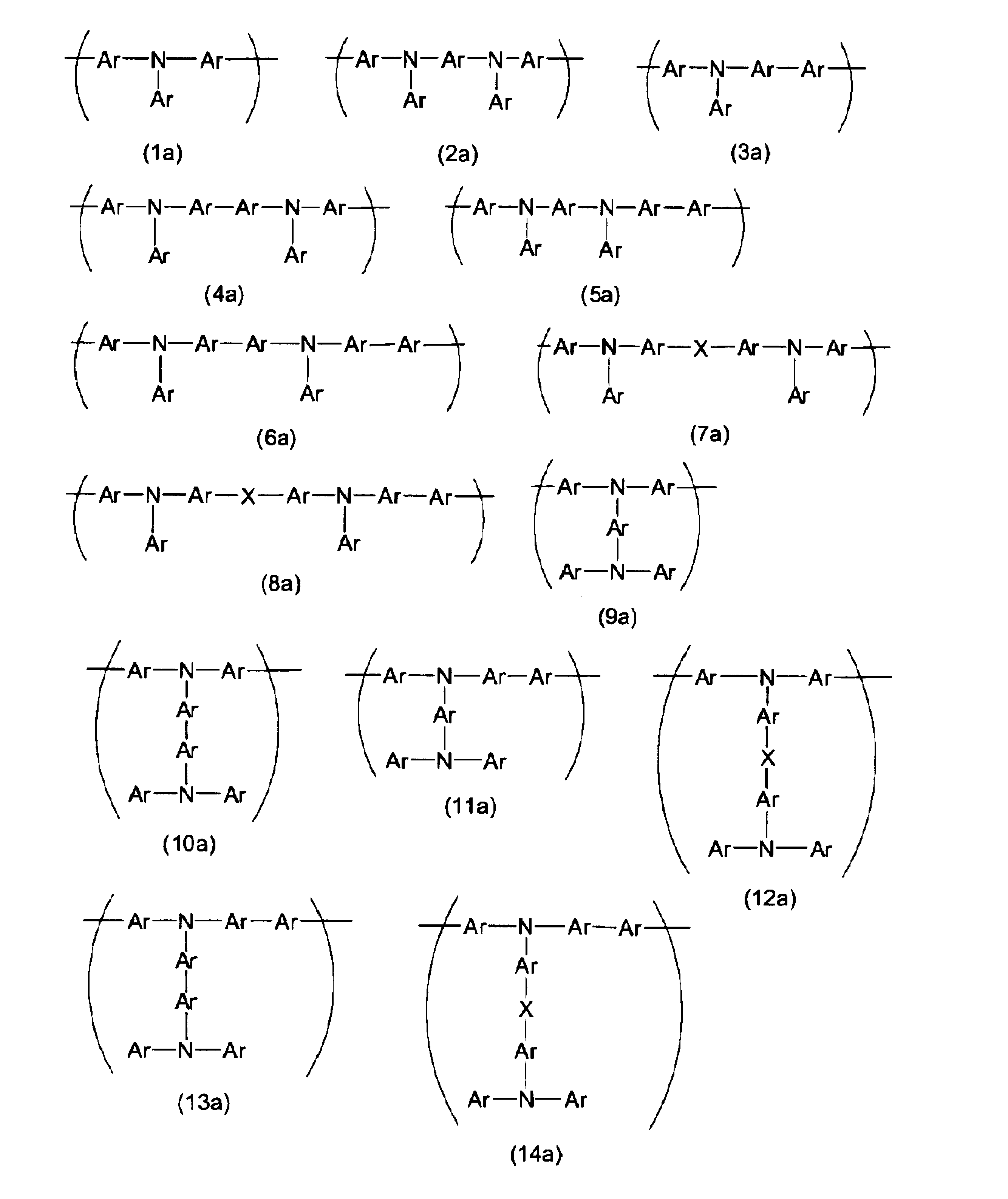
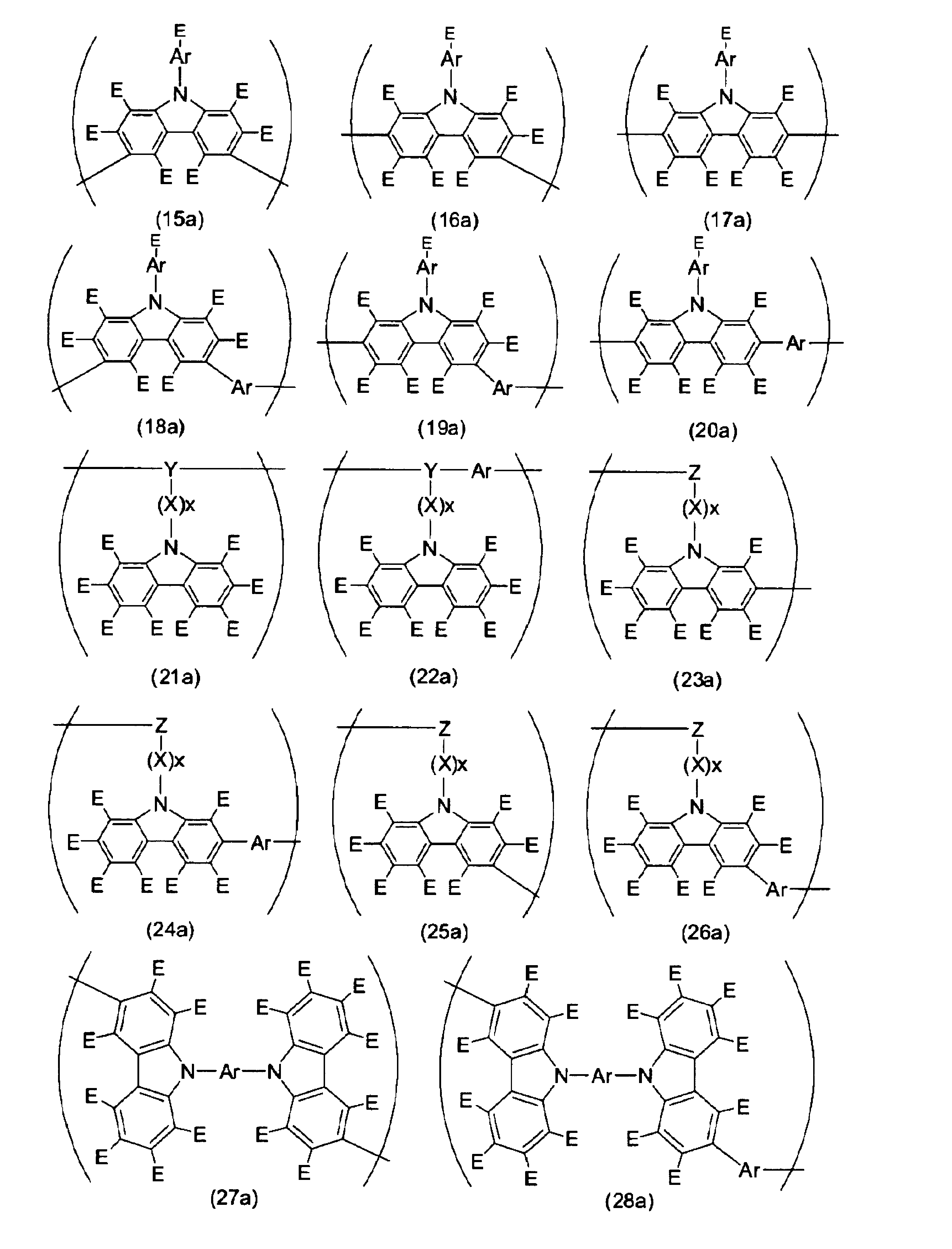


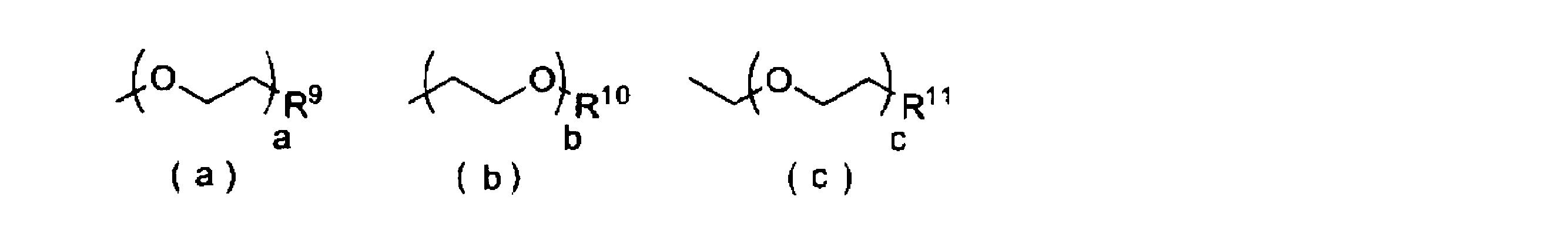


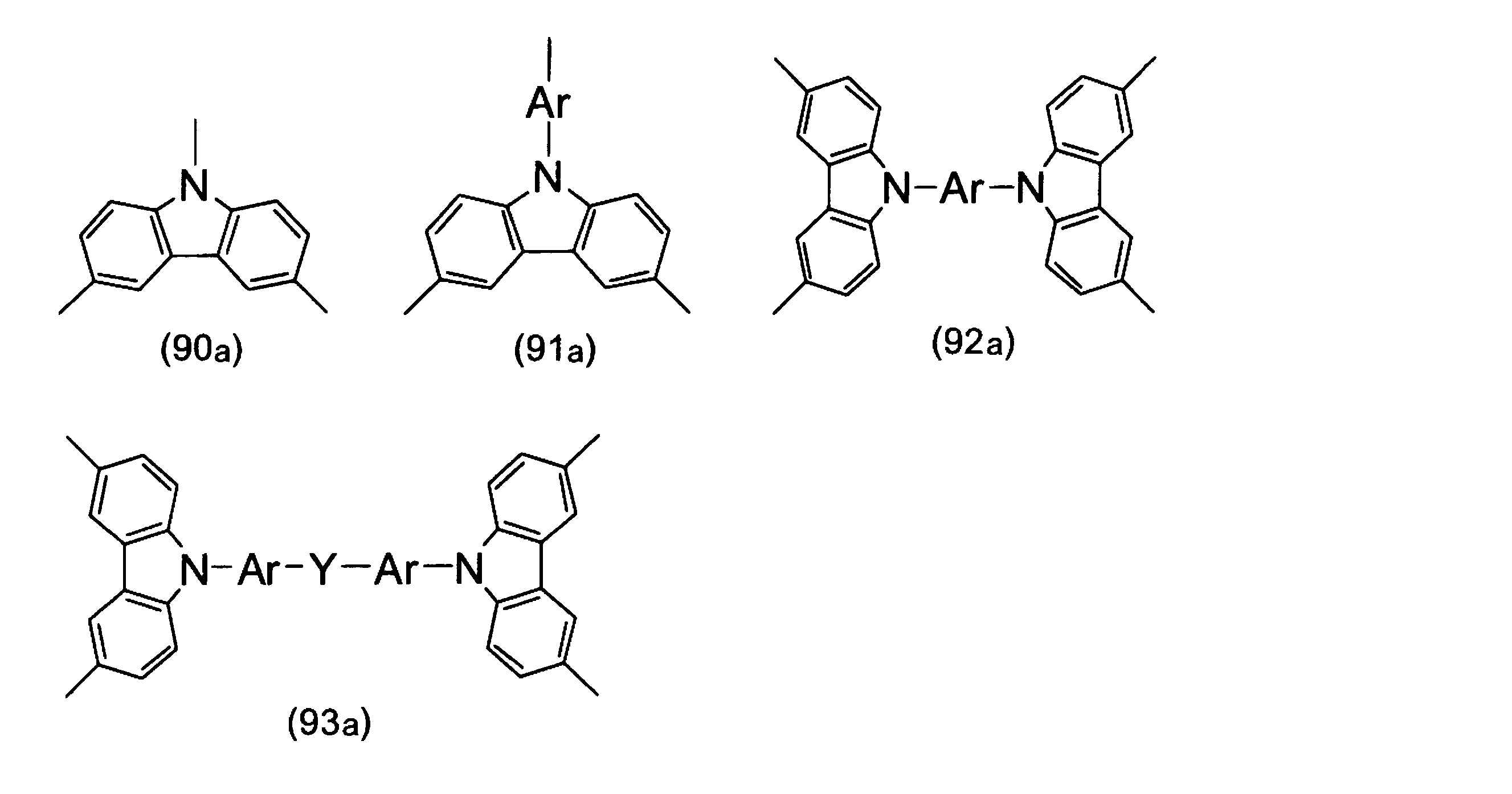
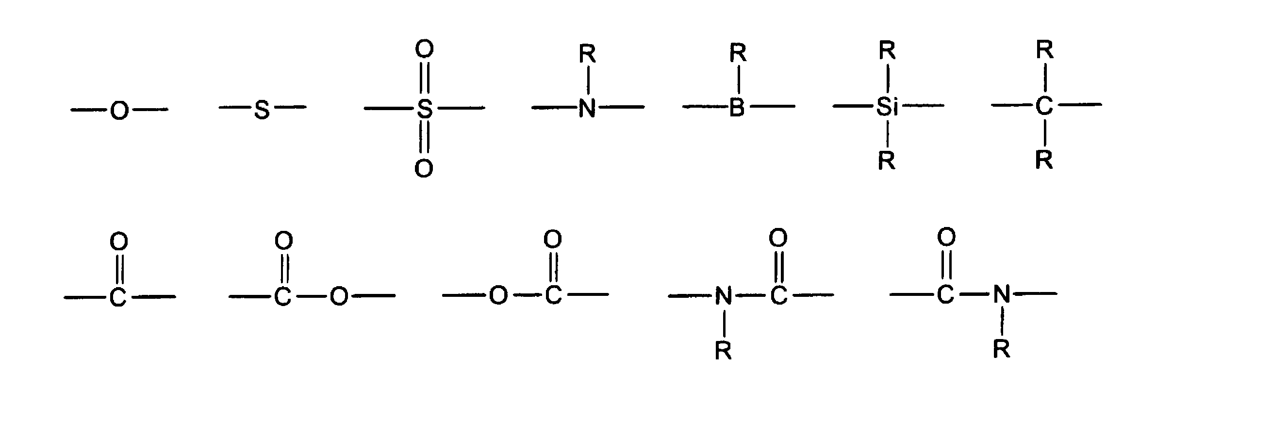


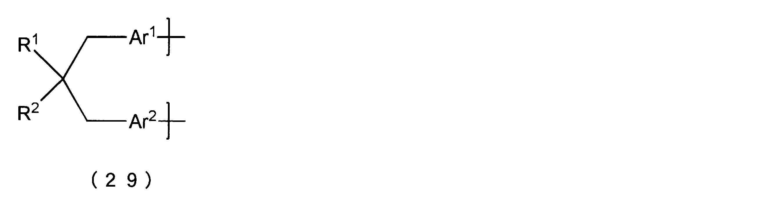
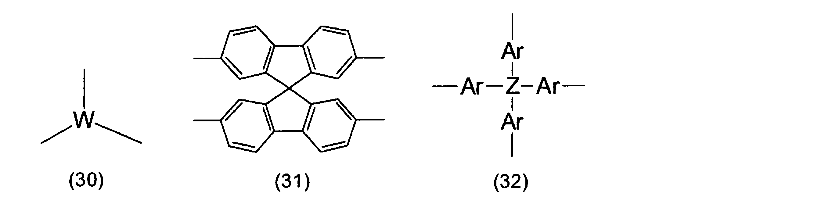
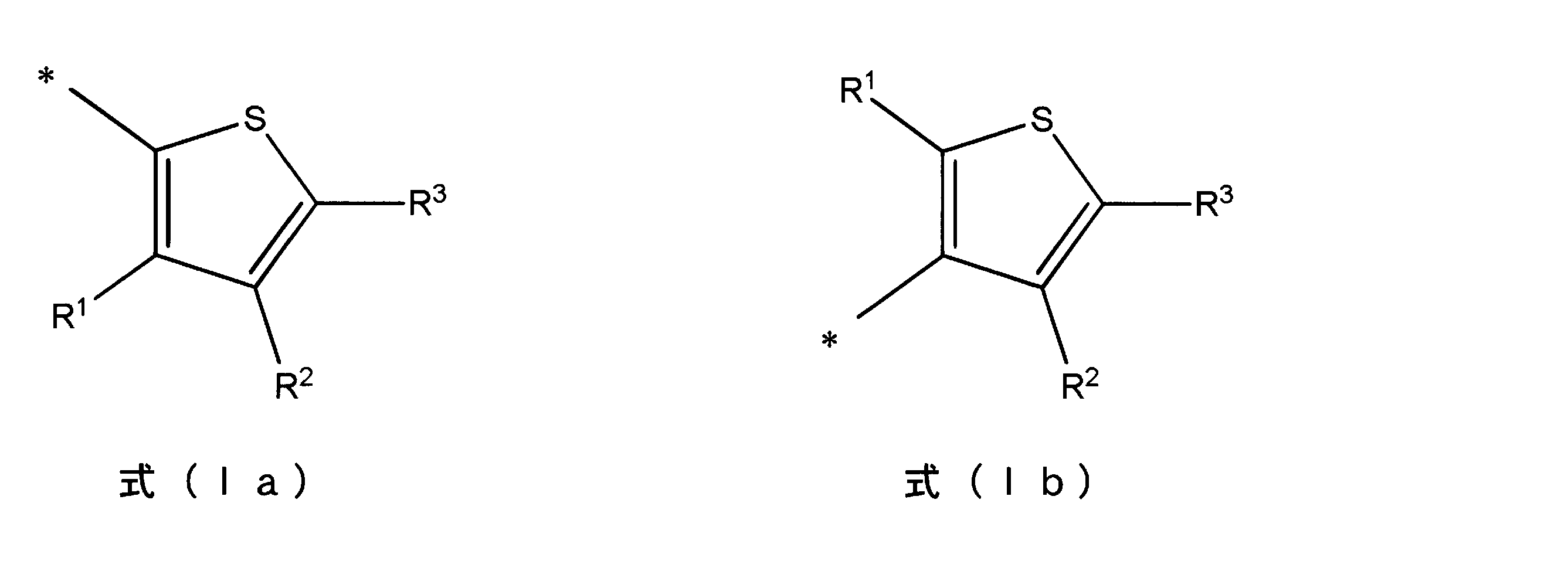
アルキル基としては、例えば、炭素数1~22個の直鎖、環状もしくは分岐アルキル基が挙げられ、直鎖アルキル基が好ましい。炭素数はより好ましくは1~10個である。

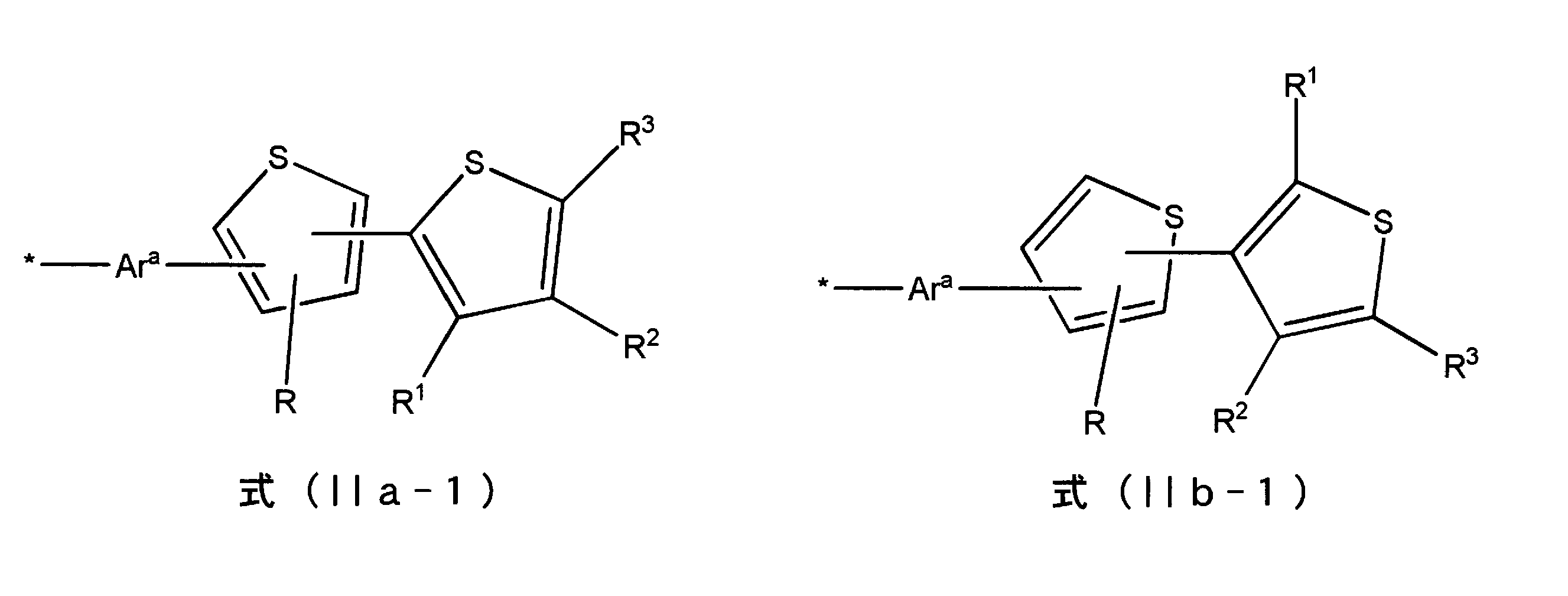


<チエニル基群(A)>


開始剤(B)は、組成物の溶解度を変化させるために用いられる。開始剤(B)としては、組成物中で酸化剤として作用し得る物質を用いることが可能である。ポリマー又はオリゴマー(A)に対して酸化剤として作用し得る物質を用いることは、正孔輸送性向上の観点から好ましい。開始剤(B)としてはカチオンとアニオンからなるオニウム塩が組成物の溶解度の変化の観点から好ましく、以下その詳細について述べる。
カチオンとしては、例えば、H+、カルベニウムイオン、アンモニウムイオン、アニリニウムイオン、ピリジニウムイオン、イミダゾリウムイオン、ピロリジニウムイオン、キノリニウムイオン、イモニウムイオン、アミニウムイオン、オキソニウムイオン、ピリリウムイオン、クロメニリウム、キサンチリウムイオン、ヨードニウムイオン、スルホニウムイオン、ホスホニウムイオン、トロピリウムイオン、遷移金属を有するカチオンなどが挙げられ、カルベニウムイオン、アンモニムイオン、アニリニウムイオン、アミニウムイオン、ヨードニウムイオン、スルホニウムイオン、トロピリウムイオンが好ましい。組成物の溶解度の変化特性及び保存安定性との両立の観点から、アンモニウムイオン、アニリニウムイオン、ヨードニウムイオン、スルホニウムイオンがより好ましい。
アニオンとしては、例えば、F-、Cl-、Br-、I-などのハロゲンイオン;OH-;ClO4 -;FSO3 -、ClSO3 -、CH3SO3 -、C6H5SO3 -、CF3SO3 -などのスルホン酸イオン類;HSO4 -、SO4 2-などの硫酸イオン類;HCO3 -、CO3 2-などの炭酸イオン類;H2PO4 -、HPO4 2-、PO4 3-などのリン酸イオン類;PF6 -、PF5OH-などのフルオロリン酸イオン類;[(CF3CF2)3PF3]-、[(CF3CF2CF2)3PF3]-、[((CF3)2CF)3PF3]-、[((CF3)2CF)2PF4]-、[((CF3)2CFCF2)3PF3]-、[((CF3)2CFCF2)2PF4]-などのフッ素化アルキルフルオロリン酸イオン類;(CF3SO2)3C-、(CF3SO2)2N-などのフルオロアルカンスルホニルメチド、イミドイオン類;BF4 -、B(C6F5)4 -、B(C6H4CF3)4 -などのホウ酸イオン類;SbF6 -、SbF5OH-などのフルオロアンチモン酸イオン類;AsF6 -、AsF5OH-などのフルオロヒ素酸イオン類;AlCl4 -、BiF6 -等が挙げられる。前述のカチオンと組み合わせて用いたときの組成物の溶解度の変化特性の観点から、PF6 -、PF5OH-などのフルオロリン酸イオン類;[(CF3CF2)3PF3]-、[(CF3CF2CF2)3PF3]-、[((CF3)2CF)3PF3]-、[((CF3)2CF)2PF4]-、[((CF3)2CFCF2)3PF3]-、[((CF3)2CFCF2)2PF4]-などのフッ素化アルキルフルオロリン酸イオン類;(CF3SO2)3C-、(CF3SO2)2N-などのフルオロアルカンスルホニルメチド、イミドイオン類;BF4 -、B(C6F5)4 -、B(C6H4CF3)4 -などのホウ酸イオン類;SbF6 -、SbF5OH-などのフルオロアンチモン酸イオン類が好ましく、なかでもホウ酸イオン類が特に好ましい。
溶解度が変化する組成物は、さらに溶媒を含んでいてもよい。溶媒としては、組成物を用いて塗布層を形成することが可能な溶媒を用いることができ、好ましくはポリマー又はオリゴマー(A)及び開始剤(B)を溶解しうる溶媒を用いることができる。
また、本発明の実施形態は、前記組成物を含む正孔輸送材料組成物に関する。
正孔輸送材料組成物とは、ポリマー又はオリゴマー(A)及び開始剤(B)と、一般的には、これらを溶解あるいは分散しうる溶媒とを含んでいればよい。溶媒の例は上述のとおりである。正孔輸送材料組成物は、さらに、低分子化合物、ドーパントとして作用し得る物質などを含んでいてもよい。
また、本発明の実施形態は、前記組成物を含むインク組成物に関する。
インク組成物とは、ポリマー又はオリゴマー(A)及び開始剤(B)と、一般的には、これらを溶解あるいは分散しうる溶媒とを含んでいればよい。溶媒の例は上述のとおりである。インク組成物は、さらに、その他の添加剤、例えば重合禁止剤、安定剤、増粘剤、ゲル化剤、難燃剤、酸化防止剤、還元防止剤、酸化剤、還元剤、表面改質剤、乳化剤、消泡剤、分散剤、界面活性剤などを含んでいてもよい。
また、本発明の実施形態は、前記溶解度が変化する組成物、正孔輸送材料組成物、又はインク組成物から形成した有機層(I)及び(II)(以下、有機層(I)及び/又は有機層(II)を単に「有機層」という場合もある。)に関する。有機層(I)は、これらの組成物を塗布することにより形成することができる。
また、本発明の実施形態は、上述の有機層を有する有機EL素子、有機光電変換素子等の有機エレクトロニクス素子に関する。有機エレクトロニクス素子は、少なくとも2つの電極、及び、電極の間に位置する有機層を有する。
さらに、本発明の実施形態は、有機EL素子を用いた表示素子及び照明装置に関する。
本発明の実施形態の有機EL素子は、前記有機層を含む。有機EL素子は、通常、発光層、陽極、陰極、及び基板を備えており、正孔注入層、電子注入層、正孔輸送層、電子輸送層などの他の層を有していてもよい。有機EL素子は、少なくとも上述の有機層を有しており、例えば、有機層を発光層及び他の層として使用することができ、好ましくは正孔注入層及び/又は正孔輸送層として使用することができる。したがって、有機EL素子の例は、陽極、正孔注入層及び/又は正孔輸送層としての有機層、発光層、及び陰極をこの順に有し、さらにこれらの層の間に任意の層を有していてもよい。以下、各層について詳細に説明する。
発光層に用いる材料としては、低分子化合物であっても、ポリマー又はオリゴマーであってもよく、デンドリマー等も使用可能である。蛍光発光を利用する低分子化合物としては、ペリレン、クマリン、ルブレン、キナクリドン、色素レーザー用色素(例えば、ローダミン、DCM1等)、アルミニウム錯体(例えば、Tris(8-hydroxyquinolinato)aluminum(III)(Alq3))、スチルベン、これらの誘導体などが挙げられる。蛍光発光を利用するポリマー又はオリゴマーとしては、ポリフルオレン、ポリフェニレン、ポリフェニレンビニレン(PPV)、ポリビニルカルバゾール(PVK)、フルオレン-ベンゾチアジアゾール共重合体、フルオレン-トリフェニルアミン共重合体、これらの誘導体及び混合物などが好適に利用できる。
塗布法により形成する場合、有機EL素子を安価に製造することができ、より好ましい。発光層を塗布法によって形成するには、燐光材料と、必要に応じてホスト材料を含む溶液を、公知の塗布法で所望の基体上に塗布することで行うことができる。塗布法としては、例えば、インクジェット法、キャスト法、浸漬法、凸版印刷、凹版印刷、オフセット印刷、平板印刷、凸版反転オフセット印刷、スクリーン印刷、グラビア印刷等の印刷法、スピンコーティング法などが挙げられる。
陰極材料としては、例えば、Li、Ca、Mg、Al、In、Cs、Ba、Mg/Ag、LiF、CsF等の金属又は金属合金であることが好ましい。
陽極としては、金属(例えば、Au)又は金属導電率を有する他の材料を使用することができる。他の材料としては、例えば、酸化物(例えば、ITO:酸化インジウム/酸化錫)、導電性高分子(例えば、ポリチオフェン-ポリスチレンスルホン酸混合物(PEDOT:PSS))が挙げられる。
電子輸送層及び電子注入層としては、例えば、フェナントロリン誘導体(例えば、2,9-Dimethyl-4,7-diphenyl-1,10-phenanthroline(BCP))、ビピリジン誘導体、ニトロ置換フルオレン誘導体、ジフェニルキノン誘導体、チオピランジオキシド誘導体、ナフタレン、ペリレンなどの縮合環テトラカルボン酸無水物、カルボジイミド、フルオレニリデンメタン誘導体、アントラキノジメタン及びアントロン誘導体、オキサジアゾール誘導体(例えば、2-(4-Biphenylyl)-5-(4-tert-butylphenyl-1,3,4-oxadiazole)(PBD))、アルミニウム錯体(例えば、Tris(8-hydroxyquinolinato)aluminum(III)(Alq3)、Bis(2-methyl-8-quninolinato)-4-phenylphenolate aluminum (III) (BAlq))などが挙げられる。さらに、上記オキサジアゾール誘導体において、オキサジアゾール環の酸素原子を硫黄原子に置換したチアジアゾール誘導体、電子吸引基として知られているキノキサリン環を有するキノキサリン誘導体も用いることができる。
有機EL素子に用いることができる基板として、ガラス、プラスチック等の種類は特に限定されることはない。また、透明の基板が好ましく、ガラス、石英、光透過性樹脂フィルム等が好ましく用いられる。樹脂フィルムを用いた場合には、有機EL素子にフレキシブル性を与えることが可能であり(つまり、フレキシブル基板)、特に好ましい。
本発明の実施形態である有機EL素子は、外気の影響を低減させて長寿命化させるため、後述する光電変換素子と同様の方法により封止されていてもよい。
有機EL素子における発光色は特に限定されるものではないが、白色発光素子は家庭用照明、車内照明、時計又は液晶のバックライト等の各種照明器具に用いることができるため好ましい。
本発明の実施形態である表示素子は、既述の有機EL素子を備えている。
例えば、赤・緑・青(RGB)の各画素に対応する素子として、前記有機EL素子を用いることで、カラーの表示素子が得られる。
画像の形成には、マトリックス状に配置した電極でパネルに配列された個々の有機EL素子を直接駆動する単純マトリックス型と、各素子に薄膜トランジスタを配置して駆動するアクティブマトリックス型とがある。前者は、構造は単純ではあるが垂直画素数に限界があるため、文字などの表示に用いられる。後者は、駆動電圧は低く電流が少なくてすみ、明るい高精細画像が得られるので、高品位のディスプレイ用として用いられる。
有機光電変換素子には、有機太陽電池及び有機光センサーが含まれ、通常、光電変換層、電極、及び基板を備えている。さらに、変換効率または空気中の安定性を向上させる目的で、バッファ層、電子輸送層などの他の層を1種以上有していてもよい。有機光電変換素子は、少なくとも上述の有機層を有しており、有機層を光電変換層及びバッファ層として使用することができ、バッファ層として使用することが好ましい。したがって、有機光電変換素子の例は、陽極、バッファ層としての有機層、光電変換層、及び陰極をこの順に有し、さらにこれらの層の間に任意の層を有していてもよい。以下に有機光電変換素子の構成について記載する。
光電変換層には、光を吸収して電荷分離を起こし、起電力を発生するものであれば任意の材料を用いることができる。特に、変換効率の観点から、p型有機半導体と、n型有機半導体とをブレンドした混合物が好ましい。
また、有機光電変換素子は、光電変換層以外に上述のバッファ層を有し、さらに電子輸送層などの層を有していてもよい。バッファ層としては、上述の有機層を用いることができ、電子輸送層としては、LiF、TiOx、ZnOx等が一般的に用いられる。
電極は、導電性を有するものであれば任意の材料を用いることが可能である。電極としては、例えば、白金、金、銀、アルミニウム、クロム、ニッケル、銅、チタン、マグネシウム、カルシウム、バリウム、ナトリウム、フッ化リチウム等の金属あるいはそれらの合金又は塩;酸化インジウム、酸化錫等の金属酸化物、あるいはその合金(ITO);ポリアニリン、ポリピロール、ポリチオフェン、ポリアセチレン等の導電性高分子;塩酸、硫酸、スルホン酸等の酸、FeCl3等のルイス酸、ヨウ素等のハロゲン原子、ナトリウム、カリウム等の金属原子などのドーパントを添加した前記導電性高分子;金属粒子、カーボンブラック、フラーレン、カーボンナノチューブ等の導電性粒子をポリマーバインダー等のマトリクスに分散した導電性の複合材料などが挙げられる。また、これらを組み合わせて用いてもよい。
基板は、各層を支持できるものであれば任意の材料を用いることが可能である。基板としては、例えば、ガラス等の無機材料;ポリエチレンテレフタレート(PET)、ポリエチレンナフタレート(PEN)、ポリエーテルスルホン(PES)、ポリイミド(PI)、ポリエーテルイミド(PEI)、シクロオレフィンポリマー(COP)、ポリフェニレンサルファイド(PPS)、ナイロン、ポリスチレン、ポリエチレン、ポリプロピレン、ポリビニルアルコール、フッ素樹脂、塩化ビニル、セルロース、ポリ塩化ビニリデン、アラミド、ポリウレタン、ポリカーボネート、ポリアリレート、ポリノルボルネン、ポリ乳酸等の有機材料;絶縁性を付与するために表面をコートあるいはラミネートしたステンレス、チタン、アルミニウム等の金属等の複合材料などが挙げられる。また、ガスバリア性の付与のために、酸化珪素、窒化珪素等の無機物を積層した基板を用いてもよい。
本発明の実施形態である有機光電変換素子は、外気の影響を低減させて長寿命化させるため、封止されていてもよい。封止に用いる材料としては、ガラス、エポキシ樹脂、アクリル樹脂、PET、PEN等のプラスチックフィルム、酸化珪素、窒化珪素等の無機物等を用いることができる。
(Pd触媒の調整)
窒素雰囲気下のグローブボックス中で、室温下、サンプル管にトリス(ジベンジリデンアセトン)ジパラジウム(73.2mg、80μmol)を秤取り、アニソール(15mL)を加え、30分間撹拌した。同様に、サンプル管にトリ-tert-ブチルホスフィン(129.6mg、640μmol)を秤取り、アニソール(5mL)を加え、5分間撹拌した。これらの溶液を混合し、室温で30分間撹拌し触媒とした。すべての溶媒は30分以上、窒素バブルにより脱気した後、使用した。
末端にチオフェン環を有するポリマーA

送液ポンプ :L-6050 (株)日立ハイテクノロジーズ
UV-Vis検出器 :L-3000 (株)日立ハイテクノロジーズ
カラム :Gelpack (R) GL-A160S/GL-A150S 日立化成工業(株)
溶離液 :THF(和光純薬製, HPLC用, 安定剤不含)
流速 :1 mL/min
カラム温度 :室温
分子量標準物質:標準ポリスチレン
末端にビチオフェンを有するポリマーB

末端にチオフェン環を有するポリマーC
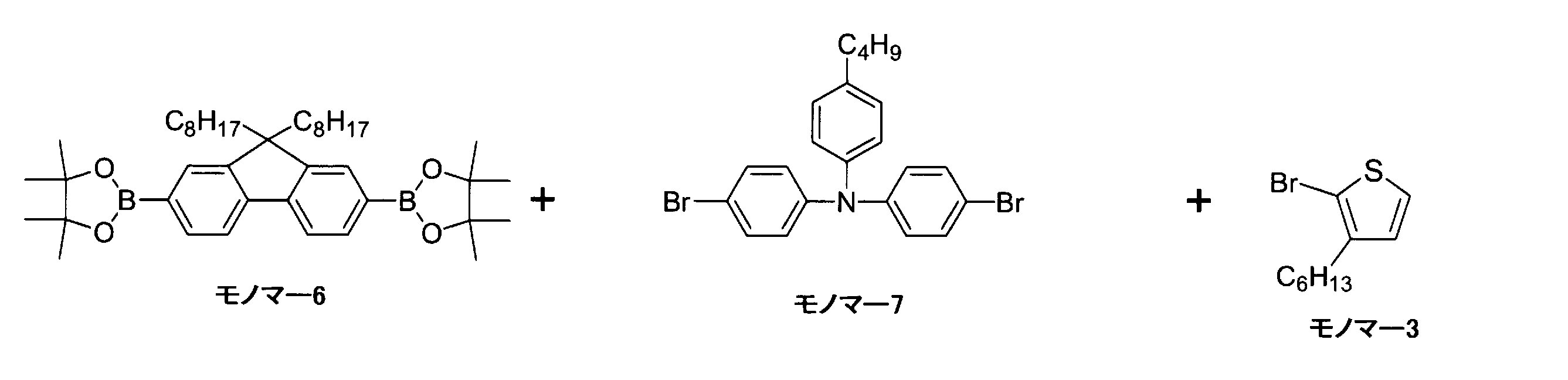
末端にチオフェン環を有するポリマーD

末端にチオフェン環を有するポリマーE

末端にチオフェン環を有するポリマーF
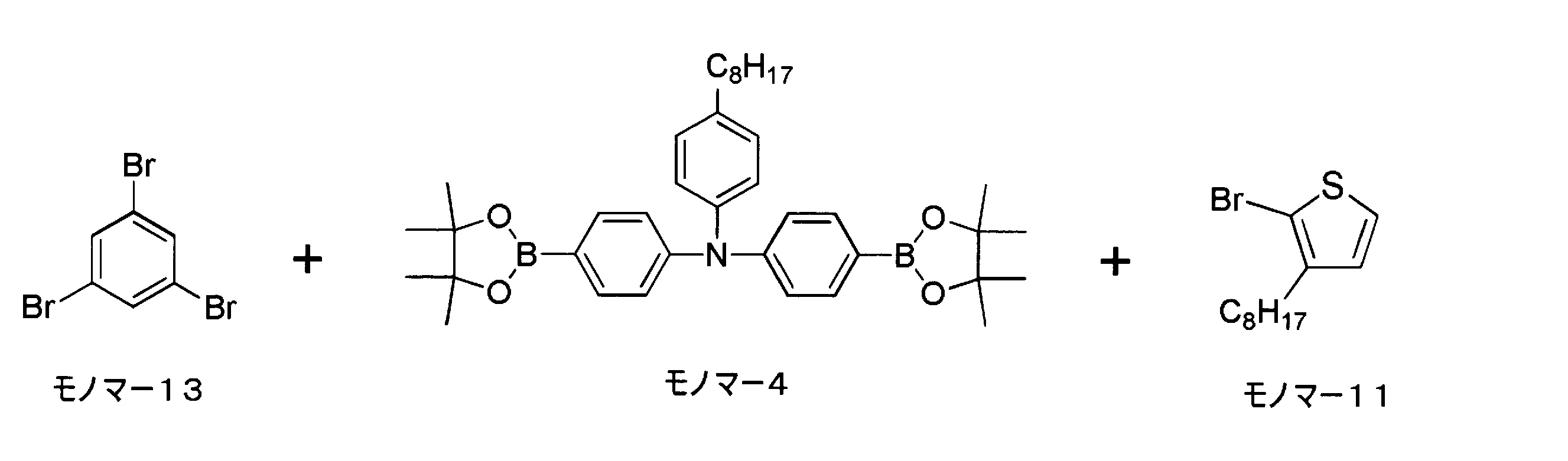
(実施例1)
上記で得たポリマーA~Fをそれぞれトルエンに溶解し(ポリマー4.5mg/465μL)、開始剤1~8の酢酸エチル溶液(50μL、開始剤濃度10μg/1μL)をそれぞれ加え、インク組成物を作製した。いずれのインク組成物も、均一な溶液として得られた。また、カチオンとしてアンモニウムイオン、アニリニウムイオン、ヨードニウムイオン、又はスルホニウムイオンを有する開始剤を用いたインク組成物は、保存安定性に特に優れていた。
開始剤を添加しない以外は、実施例1と同様の条件でインク組成物の作製を行なった。均一な溶液が得られた。
(残膜率評価)
実施例1及び比較例1で作製したインク組成物を22mm×29mm×厚さ1mmの石英ガラス板上に、室温(25℃)で、3000min-1でスピンコートし、薄膜(1)を形成した。その後、薄膜(1)をホットプレート上で210℃、10分間加熱して硬化させ、薄膜(2)(50nm)を形成した。膜厚は、株式会社テックサイエンス製 触針式段差・表面形状測定装置XP-2を用いて測定した。この薄膜(2)を石英ガラス板ごとピンセットで掴んで、トルエン(25℃)を満たした200mLビーカーに浸漬し、10秒間に基板の厚み方向に10往復振動させることによりリンスし、薄膜(3)を得た。リンス前後の薄膜の吸光度の比より、薄膜(3)の残存率(残膜率)を求めた。結果を表1にまとめた。
吸光度の測定は、分光光度計((株)日立製作所製 U-3310)を用いて行った。薄膜について、300~420nmでの極大吸収における吸光度を求めた。


(実施例2:有機EL特性)
上記で得たポリマーAをトルエン(ポリマー4.5mg/465μL)に溶解し、開始剤1の酢酸エチル溶液(50μL、開始剤濃度10μg/1μL)を加え、インク組成物を作製した。ITOを1.6mm幅にパターンニングしたガラス基板上に、このインク組成物を3000min-1でスピンコートし、薄膜を形成した。薄膜をホットプレート上で210℃、10分間加熱して硬化させ、正孔注入層(膜厚50nm)を形成した。

開始剤1を添加しない以外は、実施例2と同様な条件で有機EL素子の作製を行なった。ポリマー発光層の形成時に、正孔注入層とポリマー発光層が混ざり合い、積層構造を作製できなかった。この有機EL素子に、ITOを陽極、Alを陰極として電圧を印加したところ、均質な発光が得られなかった。
(実施例3:有機薄膜太陽電池特性)
上記で得たポリマーBをトルエン(ポリマー4.5mg/465μL)に溶解し、開始剤4の酢酸エチル溶液(50μL、開始剤濃度10μg/1μL)を加え、インク組成物を作製した。ITOを1.6mm幅にパターンニングしたガラス基板上に、このインク組成物を3000min-1でスピンコートし、薄膜を形成した。薄膜をホットプレート上で210℃、10分間加熱して硬化させ、バッファ層(膜厚50nm)を形成した。
開始剤4を添加しない以外は、実施例3と同様な条件で有機光電変換素子の作製を行なった。光電変換層形成時に、バッファ層と光電変換層が混ざり合い、積層構造を作製できなかった。実施例3と同様にエネルギー変換効率を求めた。エネルギー変換効率は0.2%であった。
(実施例4)
ITOを1.6mm幅にパターニングしたガラス基板上に、ポリマーA(100mg)、開始剤5(3.0mg)、及びアニソール(1.91mL)の混合溶液を3000min-1でスピン塗布し、薄膜を形成した。薄膜をホットプレート上で180℃、10分間加熱して電荷輸送層(膜厚125nm)を作製した。次に得られたガラス基板を真空蒸着機中に移し、電荷輸送層上にAl(膜厚100nm)を蒸着した。

これら電荷輸送性評価素子に、ITOを陽極、Alを陰極として電圧を印加し、電圧印加時の電流変化を測定した。表2に10mA/cm2通電に必要な電圧を示した。

実施例4と同様に、ポリマーA(100mg)、開始剤1(3.0mg)、及びアニソール(1.91mL)の混合溶液を用いて、電荷輸送性評価素子を作製した。
実施例4と同様に、ポリマー4(100mg)、開始剤1(3.0mg)、及びアニソール(1.91mL)の混合溶液を用いて、電荷輸送性評価素子を作製した。
これら電荷輸送性評価素子に、ITOを陽極、Alを陰極として電圧を印加し、電圧印加時の電流変化を測定した。結果を図1に示す。実施例5の電荷輸送性評価素子では、比較例5の電荷輸送性評価素子と比べ、1V以下の低電圧領域で1000倍以上の電流が流れていた。本発明の実施形態である有機層は、素子の駆動電圧の低減に有用である。
(実施例6:有機EL信頼性)
上記で得たポリマーA(10mg)、開始剤1(0.5mg)、及びトルエン(1000μL)を混合した塗布溶液を調製した。ITOを1.6mm幅にパターニングしたガラス基板上に、この塗布溶液を、3000min-1でスピンコートし、薄膜を形成した。薄膜をホットプレート上で180℃、10分間加熱して硬化させ、正孔注入層(30nm)を形成した。ここまでは、大気下で行った。
ITOを1.6mm幅にパターンニングしたガラス基板上に、PEDOT:PSS分散液(シュタルク・ヴィテック社製、AI4083 LVW142)を1500min-1でスピンコートし、ホットプレート上で空気中200℃、10分加熱して乾燥させ、正孔注入層(40nm)を形成した。その後、実施例6と同様の方法で多層構造の有機EL素子を作製した。
Claims (20)
- 正孔輸送性を有する繰り返し単位を有し、かつ、置換基を有していてもよいチエニル基を有するポリマー又はオリゴマー(A)、及び開始剤(B)を含有し、熱、光、又は熱と光の両方を加えることにより溶解度が変化する組成物。
- 正孔輸送性を有する繰り返し単位が、芳香族アミン構造を含む繰り返し単位及びカルバゾール構造を含む繰り返し単位からなる群から選択される少なくとも1種の繰り返し単位を含む請求項1記載の組成物。
- ポリマー又はオリゴマー(A)が、下記の式(Ia)で表される構造及び式(Ib)で表される構造からなる群から選択される少なくとも1種の構造を有する請求項1又は2記載の組成物。

- チエニル基を、ポリマー又はオリゴマー(A)の末端に有する請求項1~3いずれか記載の組成物。
- ポリマー又はオリゴマー(A)が、分岐構造を有し、かつ、3つ以上の末端を有するポリマー又はオリゴマーであり、全ての末端中の3つ以上にチエニル基を有する請求項1~4いずれか記載の組成物。
- ポリマー又はオリゴマー(A)が、下記の式(IIa)で表される構造、式(IIb)で表される構造、式(IIIa)で表される構造、及び式(IIIb)で表される構造からなる群から選択される少なくとも1種の構造を有する請求項1~5いずれか記載の組成物。


- 開始剤(B)が、酸化剤である請求項1~6いずれか記載の組成物。
- 開始剤(B)が、オニウム塩である請求項1~7いずれか記載の組成物。
- ポリマー又はオリゴマー(A)の重量平均分子量が、1,000~1000,000である請求項1~8いずれか記載の組成物。
- 溶媒(C)をさらに含有する請求項1~9いずれか記載の組成物。
- 請求項1~10いずれか記載の組成物を含有する正孔輸送材料組成物。
- 請求項1~10いずれか記載の組成物を含有するインク組成物。
- 請求項1~10いずれか記載の組成物、請求項11記載の正孔輸送材料組成物、又は、請求項12記載のインク組成物を、塗布することにより形成した有機層(I)。
- 請求項13記載の有機層(I)の溶解度を変化させる方法であって、前記有機層(I)に熱、光、又は熱と光の両方を加える工程を有する方法。
- 請求項13記載の有機層(I)とは異なる溶解度を有する有機層(II)であって、前記有機層(I)に熱、光、又は熱と光の両方を加えることにより得た有機層(II)。
- 少なくとも2つの電極、及び、前記電極の間に位置する請求項15記載の有機層(II)を有する有機エレクトロニクス素子。
- 陽極、請求項15記載の有機層(II)、発光層、及び陰極を有する有機エレクトロルミネセンス素子。
- 請求項17記載の有機エレクトロルミネセンス素子を用いた表示素子。
- 請求項17記載の有機エレクトロルミネセンス素子を用いた照明装置。
- 陽極、請求項15記載の有機層(II)、光電変換層、及び陰極を有する有機光電変換素子。
Priority Applications (7)
| Application Number | Priority Date | Filing Date | Title |
|---|---|---|---|
| JP2013514256A JP5288084B1 (ja) | 2011-09-26 | 2012-09-26 | 溶解度が変化する組成物、正孔輸送材料組成物、及び、これらを用いた有機エレクトロニクス素子 |
| IN3017CHN2014 IN2014CN03017A (ja) | 2011-09-26 | 2012-09-26 | |
| KR1020147008079A KR101574452B1 (ko) | 2011-09-26 | 2012-09-26 | 용해도가 변화하는 조성물, 정공 수송 재료 조성물, 및, 이들을 사용한 유기 일렉트로닉스 소자 |
| CN201280046988.4A CN103827165B (zh) | 2011-09-26 | 2012-09-26 | 溶解度发生改变的组合物、空穴传输材料组合物和使用了它们的有机电子元件 |
| EP12837270.3A EP2762514B1 (en) | 2011-09-26 | 2012-09-26 | Composition having changeable solubility, hole transport material composition, and organic electronic element produced using each of said compositions |
| US14/347,063 US9252376B2 (en) | 2011-09-26 | 2012-09-26 | Composition capable of changing its solubility, hole transport material composition, and organic electronic element using the same |
| US14/972,225 US9537101B2 (en) | 2011-09-26 | 2015-12-17 | Composition capable of changing its solubility, hole transport material composition, and organic electronic element using the same |
Applications Claiming Priority (2)
| Application Number | Priority Date | Filing Date | Title |
|---|---|---|---|
| JP2011-209610 | 2011-09-26 | ||
| JP2011209610 | 2011-09-26 |
Related Child Applications (2)
| Application Number | Title | Priority Date | Filing Date |
|---|---|---|---|
| US14/347,063 A-371-Of-International US9252376B2 (en) | 2011-09-26 | 2012-09-26 | Composition capable of changing its solubility, hole transport material composition, and organic electronic element using the same |
| US14/972,225 Division US9537101B2 (en) | 2011-09-26 | 2015-12-17 | Composition capable of changing its solubility, hole transport material composition, and organic electronic element using the same |
Publications (1)
| Publication Number | Publication Date |
|---|---|
| WO2013047581A1 true WO2013047581A1 (ja) | 2013-04-04 |
Family
ID=47995611
Family Applications (1)
| Application Number | Title | Priority Date | Filing Date |
|---|---|---|---|
| PCT/JP2012/074687 WO2013047581A1 (ja) | 2011-09-26 | 2012-09-26 | 溶解度が変化する組成物、正孔輸送材料組成物、及び、これらを用いた有機エレクトロニクス素子 |
Country Status (8)
| Country | Link |
|---|---|
| US (2) | US9252376B2 (ja) |
| EP (1) | EP2762514B1 (ja) |
| JP (2) | JP5288084B1 (ja) |
| KR (1) | KR101574452B1 (ja) |
| CN (2) | CN103827165B (ja) |
| IN (1) | IN2014CN03017A (ja) |
| TW (2) | TWI614277B (ja) |
| WO (1) | WO2013047581A1 (ja) |
Cited By (6)
| Publication number | Priority date | Publication date | Assignee | Title |
|---|---|---|---|---|
| JP2017050338A (ja) * | 2015-08-31 | 2017-03-09 | 日立化成株式会社 | 有機エレクトロニクス材料及び有機エレクトロニクス素子 |
| JP2017059718A (ja) * | 2015-09-17 | 2017-03-23 | 日立化成株式会社 | 有機エレクトロニクス材料及び該材料を含むインク組成物、並びに有機エレクトロニクス素子及び有機エレクトロルミネセンス素子 |
| JP2017066289A (ja) * | 2015-09-30 | 2017-04-06 | 日立化成株式会社 | 電荷輸送性材料、該材料を用いたインキ組成物、有機エレクトロニクス素子、有機エレクトロルミネセンス素子、表示素子、照明装置、及び表示装置 |
| JP2017123438A (ja) * | 2016-01-08 | 2017-07-13 | 日立化成株式会社 | 有機エレクトロニクス材料、有機エレクトロニクス素子、及び有機エレクトロルミネセンス素子 |
| WO2018066034A1 (ja) * | 2016-10-03 | 2018-04-12 | 日立化成株式会社 | 組成物、正孔輸送材料組成物、及びインク組成物 |
| WO2018065357A1 (en) | 2016-10-06 | 2018-04-12 | Merck Patent Gmbh | Materials for organic electroluminescent devices |
Families Citing this family (16)
| Publication number | Priority date | Publication date | Assignee | Title |
|---|---|---|---|---|
| WO2012028246A1 (en) * | 2010-09-04 | 2012-03-08 | Merck Patent Gmbh | Conjugated polymers |
| IN2014CN03017A (ja) | 2011-09-26 | 2015-07-03 | Hitachi Chemical Co Ltd | |
| WO2013081052A1 (ja) * | 2011-11-30 | 2013-06-06 | 日立化成株式会社 | 有機エレクトロニクス材料、インク組成物、及び有機エレクトロニクス素子 |
| EP2966942A4 (en) * | 2013-03-08 | 2016-12-07 | Hitachi Chemical Co Ltd | TREATMENT SOLUTION CONTAINING ION COMPOUND, ORGANIC ELECTRONIC ELEMENT, AND METHOD FOR MANUFACTURING ORGANIC ELECTRONIC ELEMENT |
| JP6551238B2 (ja) * | 2014-02-14 | 2019-07-31 | 日立化成株式会社 | ポリマー又はオリゴマー、正孔輸送材料組成物、及び、これらを用いた有機エレクトロニクス素子 |
| US10067483B1 (en) | 2014-08-28 | 2018-09-04 | Apple Inc. | Controlling electrical device based on temperature and voltage |
| JP6582786B2 (ja) * | 2015-09-17 | 2019-10-02 | 日立化成株式会社 | 組成物、電荷輸送材料、及びインク並びにそれらの利用 |
| EP3605637A1 (en) * | 2017-03-29 | 2020-02-05 | Hitachi Chemical Company, Ltd. | Charge transport material and use of same |
| CN111247656B (zh) * | 2017-10-27 | 2023-03-24 | 日立化成株式会社 | 电荷传输性聚合物及有机电子元件 |
| JP6566109B1 (ja) * | 2018-12-12 | 2019-08-28 | 住友化学株式会社 | 高分子化合物、高分子化合物の製造方法及び発光素子 |
| CN115246922A (zh) * | 2021-04-28 | 2022-10-28 | 财团法人工业技术研究院 | 聚合物及包含其的发光装置 |
| US11912816B2 (en) | 2021-04-28 | 2024-02-27 | Industrial Technology Research Institute | Polymer and light-emitting device |
| US11332579B1 (en) | 2021-11-19 | 2022-05-17 | Phillips 66 Company | Fused dithieno benzothiadiazole polymers for organic photovoltaics |
| US11326019B1 (en) | 2021-11-19 | 2022-05-10 | Phillips 66 Company | Fused dithieno benzothiadiazole polymers for organic photovoltaics |
| US11690283B2 (en) | 2021-11-19 | 2023-06-27 | Phillips 66 Company | Fused dithieno benzothiadiazole polymers for organic photovoltaics |
| US11849629B2 (en) | 2021-11-19 | 2023-12-19 | Phillips 66 Company | Fused dithieno benzothiadiazole polymers for organic photovolatics |
Citations (6)
| Publication number | Priority date | Publication date | Assignee | Title |
|---|---|---|---|---|
| JP2004199935A (ja) | 2002-12-17 | 2004-07-15 | Fuji Xerox Co Ltd | 有機電界発光素子 |
| WO2005053056A1 (en) | 2003-10-30 | 2005-06-09 | Merck Patent Gmbh | Process for improved cross-linking of an organic semiconductor layer by using a plastiser containing oxetane groups |
| JP2007302886A (ja) * | 2006-04-14 | 2007-11-22 | Hitachi Chem Co Ltd | 有機エレクトロニクス用材料及びこれを用いた有機エレクトロニクス素子、有機エレクトロルミネセンス素子 |
| JP2007311262A (ja) * | 2006-05-19 | 2007-11-29 | Mitsubishi Chemicals Corp | 電荷輸送材料組成物の製造方法、電荷輸送材料組成物、電荷輸送性薄膜、電荷輸送性薄膜の製造方法および有機電界発光素子 |
| JP2010067960A (ja) * | 2008-08-13 | 2010-03-25 | Mitsubishi Chemicals Corp | 有機電界発光素子、有機el表示装置及び有機el照明 |
| WO2011078387A1 (ja) * | 2009-12-25 | 2011-06-30 | 住友化学株式会社 | 組成物及び該組成物を用いてなる発光素子 |
Family Cites Families (9)
| Publication number | Priority date | Publication date | Assignee | Title |
|---|---|---|---|---|
| KR101072098B1 (ko) * | 2006-07-19 | 2011-10-10 | 히다치 가세고교 가부시끼가이샤 | 유기 일렉트로닉스용 재료, 유기 일렉트로닉스 소자 및 유기 일렉트로루미네센스 소자 |
| CN101490864A (zh) * | 2006-07-19 | 2009-07-22 | 日立化成工业株式会社 | 有机电子材料、有机电子元件和有机电致发光元件 |
| EP3182479B1 (en) * | 2008-02-15 | 2018-10-03 | Mitsubishi Chemical Corporation | Conjugated polymer for organic electroluminescence element |
| WO2009126918A1 (en) * | 2008-04-11 | 2009-10-15 | Plextronics, Inc. | Doped conjugated polymers, devices, and methods of making devices |
| KR101762964B1 (ko) * | 2008-10-27 | 2017-07-28 | 닛산 가가쿠 고교 가부시키 가이샤 | 전하 주입 및 수송 층 |
| CN106957410B (zh) * | 2009-06-01 | 2019-06-18 | 日立化成工业株式会社 | 有机电子材料、组合物、薄膜、有机电子元件、有机电致发光元件、照明装置及显示装置 |
| JP5332934B2 (ja) * | 2009-06-18 | 2013-11-06 | 住友化学株式会社 | 有機光電変換素子 |
| IN2014CN03017A (ja) * | 2011-09-26 | 2015-07-03 | Hitachi Chemical Co Ltd | |
| JP2013072022A (ja) | 2011-09-28 | 2013-04-22 | Kuraray Co Ltd | 導電性インク及びその製造方法 |
-
2012
- 2012-09-26 IN IN3017CHN2014 patent/IN2014CN03017A/en unknown
- 2012-09-26 KR KR1020147008079A patent/KR101574452B1/ko active IP Right Grant
- 2012-09-26 US US14/347,063 patent/US9252376B2/en active Active
- 2012-09-26 TW TW101135378A patent/TWI614277B/zh active
- 2012-09-26 CN CN201280046988.4A patent/CN103827165B/zh active Active
- 2012-09-26 CN CN201610444736.7A patent/CN105885020B/zh active Active
- 2012-09-26 JP JP2013514256A patent/JP5288084B1/ja active Active
- 2012-09-26 WO PCT/JP2012/074687 patent/WO2013047581A1/ja active Application Filing
- 2012-09-26 TW TW106101646A patent/TWI626255B/zh active
- 2012-09-26 EP EP12837270.3A patent/EP2762514B1/en active Active
-
2013
- 2013-06-05 JP JP2013118989A patent/JP5737335B2/ja active Active
-
2015
- 2015-12-17 US US14/972,225 patent/US9537101B2/en active Active
Patent Citations (6)
| Publication number | Priority date | Publication date | Assignee | Title |
|---|---|---|---|---|
| JP2004199935A (ja) | 2002-12-17 | 2004-07-15 | Fuji Xerox Co Ltd | 有機電界発光素子 |
| WO2005053056A1 (en) | 2003-10-30 | 2005-06-09 | Merck Patent Gmbh | Process for improved cross-linking of an organic semiconductor layer by using a plastiser containing oxetane groups |
| JP2007302886A (ja) * | 2006-04-14 | 2007-11-22 | Hitachi Chem Co Ltd | 有機エレクトロニクス用材料及びこれを用いた有機エレクトロニクス素子、有機エレクトロルミネセンス素子 |
| JP2007311262A (ja) * | 2006-05-19 | 2007-11-29 | Mitsubishi Chemicals Corp | 電荷輸送材料組成物の製造方法、電荷輸送材料組成物、電荷輸送性薄膜、電荷輸送性薄膜の製造方法および有機電界発光素子 |
| JP2010067960A (ja) * | 2008-08-13 | 2010-03-25 | Mitsubishi Chemicals Corp | 有機電界発光素子、有機el表示装置及び有機el照明 |
| WO2011078387A1 (ja) * | 2009-12-25 | 2011-06-30 | 住友化学株式会社 | 組成物及び該組成物を用いてなる発光素子 |
Non-Patent Citations (10)
| Title |
|---|
| A. SUZUKI, SYNTHETIC COMMUNICATIONS, vol. 11, no. 7, 1981, pages 513 |
| ADACHI ET AL., APPL. PHYS. LETT., vol. 78, no. 11, 2001, pages 1622 |
| CARLOS A. ZUNIGA; STEPHEN BARLOW; SETH R. MARDER: "Approaches to Solution-Processed Multilayer Organic Light-Emitting Diodes Based on Cross-Linking", CHEM. MATER., vol. 23, no. 3, 2011, pages 658 - 681 |
| GUOLI TU ET AL.: "Conjugated triblock copolymers containing both electron-donor and electron- acceptor blocks", MACROMOLECULES, vol. 39, no. 13, 2006, pages 4327 - 4331, XP055147677 * |
| M. ZEMBAYASHI ET AL., TET. LETT., vol. 47, 1977, pages 4089 |
| M.A. BALDO ET AL., APPLIED PHYSICS LETTERS, vol. 75, 1999, pages 4 |
| M.A. BALDO ET AL., NATURE, vol. 395, 1998, pages 151 |
| M.A. BALDO ET AL., NATURE, vol. 403, 2000, pages 750 |
| See also references of EP2762514A4 |
| T. YAMAMOTO ET AL., BULL. CHEM. SOC. JPN., vol. 51, no. 7, 1978, pages 2091 |
Cited By (10)
| Publication number | Priority date | Publication date | Assignee | Title |
|---|---|---|---|---|
| JP2017050338A (ja) * | 2015-08-31 | 2017-03-09 | 日立化成株式会社 | 有機エレクトロニクス材料及び有機エレクトロニクス素子 |
| JP2017059718A (ja) * | 2015-09-17 | 2017-03-23 | 日立化成株式会社 | 有機エレクトロニクス材料及び該材料を含むインク組成物、並びに有機エレクトロニクス素子及び有機エレクトロルミネセンス素子 |
| JP2017066289A (ja) * | 2015-09-30 | 2017-04-06 | 日立化成株式会社 | 電荷輸送性材料、該材料を用いたインキ組成物、有機エレクトロニクス素子、有機エレクトロルミネセンス素子、表示素子、照明装置、及び表示装置 |
| JP2017123438A (ja) * | 2016-01-08 | 2017-07-13 | 日立化成株式会社 | 有機エレクトロニクス材料、有機エレクトロニクス素子、及び有機エレクトロルミネセンス素子 |
| WO2018066034A1 (ja) * | 2016-10-03 | 2018-04-12 | 日立化成株式会社 | 組成物、正孔輸送材料組成物、及びインク組成物 |
| CN109790360A (zh) * | 2016-10-03 | 2019-05-21 | 日立化成株式会社 | 组合物、空穴传输材料组合物和油墨组合物 |
| JPWO2018066034A1 (ja) * | 2016-10-03 | 2019-08-08 | 日立化成株式会社 | 組成物、正孔輸送材料組成物、及びインク組成物 |
| US11118005B2 (en) | 2016-10-03 | 2021-09-14 | Showa Denko Materials Co., Ltd. | Composition, hole transport material composition, and ink composition |
| CN109790360B (zh) * | 2016-10-03 | 2022-01-25 | 昭和电工材料株式会社 | 组合物、空穴传输材料组合物和油墨组合物 |
| WO2018065357A1 (en) | 2016-10-06 | 2018-04-12 | Merck Patent Gmbh | Materials for organic electroluminescent devices |
Also Published As
| Publication number | Publication date |
|---|---|
| JPWO2013047581A1 (ja) | 2015-03-26 |
| KR101574452B1 (ko) | 2015-12-03 |
| TWI626255B (zh) | 2018-06-11 |
| CN105885020B (zh) | 2018-04-10 |
| US9537101B2 (en) | 2017-01-03 |
| KR20140068103A (ko) | 2014-06-05 |
| JP5737335B2 (ja) | 2015-06-17 |
| CN103827165A (zh) | 2014-05-28 |
| EP2762514A4 (en) | 2015-04-15 |
| CN105885020A (zh) | 2016-08-24 |
| IN2014CN03017A (ja) | 2015-07-03 |
| TW201319114A (zh) | 2013-05-16 |
| EP2762514A1 (en) | 2014-08-06 |
| US9252376B2 (en) | 2016-02-02 |
| TW201718695A (zh) | 2017-06-01 |
| CN103827165B (zh) | 2016-06-29 |
| JP5288084B1 (ja) | 2013-09-11 |
| EP2762514B1 (en) | 2021-03-17 |
| US20160111647A1 (en) | 2016-04-21 |
| TWI614277B (zh) | 2018-02-11 |
| JP2013229614A (ja) | 2013-11-07 |
| US20140231791A1 (en) | 2014-08-21 |
Similar Documents
| Publication | Publication Date | Title |
|---|---|---|
| JP5737335B2 (ja) | 溶解度が変化する組成物、正孔輸送材料組成物、及び、これらを用いた有機エレクトロニクス素子 | |
| KR102324619B1 (ko) | 폴리머 또는 올리고머, 정공 수송 재료 조성물 및 이들을 이용한 유기 일렉트로닉스 소자 | |
| TWI764881B (zh) | 有機電子材料、有機電子元件及有機電致發光元件 | |
| JP6331462B2 (ja) | 有機エレクトロニクス素子の製造方法 | |
| WO2016076375A1 (ja) | 有機エレクトロルミネセンス素子及びその製造方法 | |
| JP6136366B2 (ja) | 有機エレクトロニクス素子及びその製造方法 | |
| JP6827654B2 (ja) | 有機エレクトロニクス材料、インク組成物、有機層、及び有機エレクトロニクス素子 | |
| JP6221230B2 (ja) | 有機エレクトロニクス素子及びその製造方法 | |
| JP6094058B2 (ja) | 有機エレクトロニクス材料、インク組成物、有機エレクトロニクス素子、有機エレクトロルミネセンス素子、及び光電変換素子 | |
| JP5939423B2 (ja) | ポリマー又はオリゴマー、及びこれを用いた有機エレクトロニクス素子 | |
| JP6123288B2 (ja) | 溶解度が変化する組成物、正孔輸送材料組成物、及び、これらを用いた有機エレクトロニクス素子 | |
| JP6690241B2 (ja) | 有機エレクトロニクス材料及びその利用 | |
| WO2017212560A1 (ja) | 有機エレクトロニクス材料及び有機エレクトロニクス素子 | |
| JP2020145235A (ja) | 有機エレクトロニクス材料及びその利用 | |
| JP2020145236A (ja) | 有機エレクトロニクス材料及びその利用 | |
| JP2020098876A (ja) | 有機エレクトロニクス材料 |
Legal Events
| Date | Code | Title | Description |
|---|---|---|---|
| ENP | Entry into the national phase |
Ref document number: 2013514256 Country of ref document: JP Kind code of ref document: A |
|
| 121 | Ep: the epo has been informed by wipo that ep was designated in this application |
Ref document number: 12837270 Country of ref document: EP Kind code of ref document: A1 |
|
| WWE | Wipo information: entry into national phase |
Ref document number: 14347063 Country of ref document: US |
|
| NENP | Non-entry into the national phase |
Ref country code: DE |
|
| ENP | Entry into the national phase |
Ref document number: 20147008079 Country of ref document: KR Kind code of ref document: A |
|
| WWE | Wipo information: entry into national phase |
Ref document number: 2012837270 Country of ref document: EP |