WO2013021992A1 - アクティブマトリクス型表示装置 - Google Patents
アクティブマトリクス型表示装置 Download PDFInfo
- Publication number
- WO2013021992A1 WO2013021992A1 PCT/JP2012/070067 JP2012070067W WO2013021992A1 WO 2013021992 A1 WO2013021992 A1 WO 2013021992A1 JP 2012070067 W JP2012070067 W JP 2012070067W WO 2013021992 A1 WO2013021992 A1 WO 2013021992A1
- Authority
- WO
- WIPO (PCT)
- Prior art keywords
- wiring
- wirings
- common
- terminals
- active matrix
- Prior art date
- Legal status (The legal status is an assumption and is not a legal conclusion. Google has not performed a legal analysis and makes no representation as to the accuracy of the status listed.)
- Ceased
Links
Images







Classifications
-
- G—PHYSICS
- G02—OPTICS
- G02F—OPTICAL DEVICES OR ARRANGEMENTS FOR THE CONTROL OF LIGHT BY MODIFICATION OF THE OPTICAL PROPERTIES OF THE MEDIA OF THE ELEMENTS INVOLVED THEREIN; NON-LINEAR OPTICS; FREQUENCY-CHANGING OF LIGHT; OPTICAL LOGIC ELEMENTS; OPTICAL ANALOGUE/DIGITAL CONVERTERS
- G02F1/00—Devices or arrangements for the control of the intensity, colour, phase, polarisation or direction of light arriving from an independent light source, e.g. switching, gating or modulating; Non-linear optics
- G02F1/01—Devices or arrangements for the control of the intensity, colour, phase, polarisation or direction of light arriving from an independent light source, e.g. switching, gating or modulating; Non-linear optics for the control of the intensity, phase, polarisation or colour
- G02F1/13—Devices or arrangements for the control of the intensity, colour, phase, polarisation or direction of light arriving from an independent light source, e.g. switching, gating or modulating; Non-linear optics for the control of the intensity, phase, polarisation or colour based on liquid crystals, e.g. single liquid crystal display cells
- G02F1/133—Constructional arrangements; Operation of liquid crystal cells; Circuit arrangements
- G02F1/136—Liquid crystal cells structurally associated with a semi-conducting layer or substrate, e.g. cells forming part of an integrated circuit
- G02F1/1362—Active matrix addressed cells
- G02F1/136286—Wiring, e.g. gate line, drain line
-
- G—PHYSICS
- G02—OPTICS
- G02F—OPTICAL DEVICES OR ARRANGEMENTS FOR THE CONTROL OF LIGHT BY MODIFICATION OF THE OPTICAL PROPERTIES OF THE MEDIA OF THE ELEMENTS INVOLVED THEREIN; NON-LINEAR OPTICS; FREQUENCY-CHANGING OF LIGHT; OPTICAL LOGIC ELEMENTS; OPTICAL ANALOGUE/DIGITAL CONVERTERS
- G02F1/00—Devices or arrangements for the control of the intensity, colour, phase, polarisation or direction of light arriving from an independent light source, e.g. switching, gating or modulating; Non-linear optics
- G02F1/01—Devices or arrangements for the control of the intensity, colour, phase, polarisation or direction of light arriving from an independent light source, e.g. switching, gating or modulating; Non-linear optics for the control of the intensity, phase, polarisation or colour
- G02F1/13—Devices or arrangements for the control of the intensity, colour, phase, polarisation or direction of light arriving from an independent light source, e.g. switching, gating or modulating; Non-linear optics for the control of the intensity, phase, polarisation or colour based on liquid crystals, e.g. single liquid crystal display cells
- G02F1/133—Constructional arrangements; Operation of liquid crystal cells; Circuit arrangements
- G02F1/1333—Constructional arrangements; Manufacturing methods
- G02F1/1345—Conductors connecting electrodes to cell terminals
-
- G—PHYSICS
- G02—OPTICS
- G02F—OPTICAL DEVICES OR ARRANGEMENTS FOR THE CONTROL OF LIGHT BY MODIFICATION OF THE OPTICAL PROPERTIES OF THE MEDIA OF THE ELEMENTS INVOLVED THEREIN; NON-LINEAR OPTICS; FREQUENCY-CHANGING OF LIGHT; OPTICAL LOGIC ELEMENTS; OPTICAL ANALOGUE/DIGITAL CONVERTERS
- G02F1/00—Devices or arrangements for the control of the intensity, colour, phase, polarisation or direction of light arriving from an independent light source, e.g. switching, gating or modulating; Non-linear optics
- G02F1/01—Devices or arrangements for the control of the intensity, colour, phase, polarisation or direction of light arriving from an independent light source, e.g. switching, gating or modulating; Non-linear optics for the control of the intensity, phase, polarisation or colour
- G02F1/13—Devices or arrangements for the control of the intensity, colour, phase, polarisation or direction of light arriving from an independent light source, e.g. switching, gating or modulating; Non-linear optics for the control of the intensity, phase, polarisation or colour based on liquid crystals, e.g. single liquid crystal display cells
- G02F1/1306—Details
- G02F1/1309—Repairing; Testing
-
- G—PHYSICS
- G02—OPTICS
- G02F—OPTICAL DEVICES OR ARRANGEMENTS FOR THE CONTROL OF LIGHT BY MODIFICATION OF THE OPTICAL PROPERTIES OF THE MEDIA OF THE ELEMENTS INVOLVED THEREIN; NON-LINEAR OPTICS; FREQUENCY-CHANGING OF LIGHT; OPTICAL LOGIC ELEMENTS; OPTICAL ANALOGUE/DIGITAL CONVERTERS
- G02F1/00—Devices or arrangements for the control of the intensity, colour, phase, polarisation or direction of light arriving from an independent light source, e.g. switching, gating or modulating; Non-linear optics
- G02F1/01—Devices or arrangements for the control of the intensity, colour, phase, polarisation or direction of light arriving from an independent light source, e.g. switching, gating or modulating; Non-linear optics for the control of the intensity, phase, polarisation or colour
- G02F1/13—Devices or arrangements for the control of the intensity, colour, phase, polarisation or direction of light arriving from an independent light source, e.g. switching, gating or modulating; Non-linear optics for the control of the intensity, phase, polarisation or colour based on liquid crystals, e.g. single liquid crystal display cells
- G02F1/133—Constructional arrangements; Operation of liquid crystal cells; Circuit arrangements
- G02F1/136—Liquid crystal cells structurally associated with a semi-conducting layer or substrate, e.g. cells forming part of an integrated circuit
- G02F1/1362—Active matrix addressed cells
- G02F1/136259—Repairing; Defects
-
- G—PHYSICS
- G02—OPTICS
- G02F—OPTICAL DEVICES OR ARRANGEMENTS FOR THE CONTROL OF LIGHT BY MODIFICATION OF THE OPTICAL PROPERTIES OF THE MEDIA OF THE ELEMENTS INVOLVED THEREIN; NON-LINEAR OPTICS; FREQUENCY-CHANGING OF LIGHT; OPTICAL LOGIC ELEMENTS; OPTICAL ANALOGUE/DIGITAL CONVERTERS
- G02F1/00—Devices or arrangements for the control of the intensity, colour, phase, polarisation or direction of light arriving from an independent light source, e.g. switching, gating or modulating; Non-linear optics
- G02F1/01—Devices or arrangements for the control of the intensity, colour, phase, polarisation or direction of light arriving from an independent light source, e.g. switching, gating or modulating; Non-linear optics for the control of the intensity, phase, polarisation or colour
- G02F1/13—Devices or arrangements for the control of the intensity, colour, phase, polarisation or direction of light arriving from an independent light source, e.g. switching, gating or modulating; Non-linear optics for the control of the intensity, phase, polarisation or colour based on liquid crystals, e.g. single liquid crystal display cells
- G02F1/133—Constructional arrangements; Operation of liquid crystal cells; Circuit arrangements
- G02F1/136—Liquid crystal cells structurally associated with a semi-conducting layer or substrate, e.g. cells forming part of an integrated circuit
- G02F1/1362—Active matrix addressed cells
- G02F1/136259—Repairing; Defects
- G02F1/136272—Auxiliary lines
Definitions
- the present invention relates to an active matrix display device.
- Patent Document 1 Japanese Patent Application Laid-Open No. 2003-222895 (Patent Document 1) and Japanese Patent Application Laid-Open No. 2005-249993 (Patent Document 2) are disclosed as prior documents disclosing devices having spare wiring. is there.
- the liquid crystal display device described in Patent Document 1 is a spare for correcting a defect in a display region that passes between input / output terminals in an IC (integrated circuit) mounting portion on a TFT (thin film transistor) array substrate. Wiring is provided.
- a through terminal including an input side terminal and an output side terminal that are electrically connected through the inside of the IC that drives the active matrix element is provided.
- spare wiring is connected to the output side of the through terminal, and a batch stipple line connected for each of RGB used for image inspection is connected to the input side of the through terminal.
- the batch stipple line is cut by a laser or the like before mounting the IC that drives the active matrix element. After mounting the IC that drives the active matrix element, the circuit is configured only by the wiring connected to the through terminals.
- a short-circuit wiring between terminals connecting an input wiring to a TFT and a wiring on the FPC (Flexible Printed Circuits) substrate side is cut by laser irradiation. If there is an input wiring to the TFT that has a disconnection defect, correct the disconnected terminal short-circuit wiring with a metal complex, or skip the laser and skip some input terminal short-circuit wiring. Repair is done by cutting the short circuit wiring between other input terminals.
- the present invention has been made in view of the above problems, and provides an active matrix display device that can be manufactured inexpensively and can be easily repaired, and the configuration of a mounted driver can be simplified. For the purpose.
- the active matrix display device includes an active matrix substrate, a driver mounted on the active matrix substrate, and an external substrate electrically connected to the active matrix substrate.
- the active matrix substrate includes a plurality of first wirings extending in parallel to each other at least in the display region, and a plurality of second wirings extending in parallel to each other in the display region and intersecting the plurality of first wirings via an insulating film. And have.
- the active matrix substrate is located on the display region side in the terminal region located outside the display region on one end side of the plurality of first wires, arranged in the extending direction of the plurality of second wires, and a signal from the driver
- a plurality of first transmission terminals that are respectively sent to a plurality of first wirings, and a display region side in a terminal region that is located outside a display region on one end side of the plurality of first wirings.
- a plurality of second transmission terminals are arranged in the extending direction and send signals from the driver to the plurality of second wirings, respectively.
- the active matrix substrate includes a plurality of first extraction wirings that respectively connect one end side of the plurality of first wirings and the plurality of first transmission terminals, one end side of at least a part of the plurality of second wirings, and the one end thereof. And a plurality of second lead wires respectively connecting the second transmission terminals located on the side.
- the active matrix substrate is electrically connected to the plurality of second lead wirings and supplies a signal to at least a part of the plurality of second wirings, and is opposite to the display region side in the terminal region. And a plurality of output terminals for outputting signals to the driver.
- the active matrix substrate has a terminal group including a plurality of input terminals to which signals are input from an external substrate, located on the side opposite to the display region side when viewed from the plurality of output terminals in the terminal region.
- the active matrix substrate is included in the terminal group and is included in the first common wiring terminal for inputting a signal passing through the plurality of first transmission terminals, and is included in the terminal group and connected to the second lead wiring.
- a second common wiring terminal for inputting signals passing through the plurality of second transmission terminals.
- first common wiring having a first extending portion connected to the first common wiring terminal and extending so as to separate the plurality of first transmission terminals and the plurality of output terminals
- second common wiring having a second extending portion extending so as to divide between the plurality of second transmission terminals and the plurality of output terminals.
- the active matrix substrate is connected to the plurality of first connection wirings provided between each of the plurality of first transmission terminals and the first extension portion of the first common wiring, and the second lead wiring.
- a plurality of second connection wirings provided between each of the plurality of second transmission terminals and the second extending portion of the second common wiring; Furthermore, the active matrix substrate intersects with the second common wiring through the insulating film and intersects with any of the plurality of first connection wirings through the insulating film, and the plurality of first wirings. Crossing one of the plurality of redundant portions located outside the display area via an insulating film and outside the plurality of second lead lines and the first drive circuit in plan view And a second auxiliary wiring that is electrically connected to the second common wiring.
- the active matrix substrate includes a first inhibition unit that inhibits electrical connection between the plurality of first transmission terminals and the first common wiring in the middle of each of the plurality of first connection wirings.
- Each of the second connection wirings has a second obstruction part that obstructs the electrical connection between the plurality of second transmission terminals connected to the second lead-out wiring and the second common wiring.
- the plurality of intersecting portions where the first spare wiring and the plurality of first connection wirings intersect are located on the plurality of first transmission terminal sides from the first obstruction portion in each of the plurality of first connection wirings. Yes.
- the active matrix substrate includes a plurality of third lead wires connected to the other end side of at least a part of the remaining portions of the plurality of second wires that are not connected to the plurality of second lead wires. And a second drive circuit that is electrically connected to the plurality of third lead wires and supplies a signal to at least a part of the remaining portions of the plurality of second wires.
- the active matrix substrate is included in the terminal group, and a third common wiring terminal for inputting signals passing through the plurality of second transmission terminals connected to the third lead wiring, and a third common wiring terminal And a third common wiring having a third extending portion extending so as to divide the plurality of second transmission terminals connected to the third lead wiring and the plurality of output terminals.
- the active matrix substrate includes a plurality of third connection wirings provided between each of the plurality of second transmission terminals connected to the third lead wiring and the third extending portion of the third common wiring; It further has a third spare wiring that intersects with the third common wiring through the insulating film and intersects with any of the plurality of first connection wirings through the insulating film.
- the active matrix substrate intersects with any one of the plurality of redundant portions located on the other end side of each of the plurality of first wirings and outside the display region via an insulating film, and in a plan view, A fourth auxiliary wiring that is located outside the third lead wiring and the second drive circuit and can be electrically connected to the third common wiring is further included.
- Each of the plurality of third connection wirings has a third obstruction part that obstructs the electrical connection between the plurality of second transmission terminals connected to the third lead wiring and the third common wiring.
- the active matrix substrate has a plurality of first common wiring terminals and a plurality of first common wirings.
- Each of the plurality of first common wirings has a first extending portion that is connected to the plurality of first common wiring terminals and extends to divide the plurality of first transmission terminals and the plurality of output terminals.
- the second spare wiring intersects with the second common wiring through a connection or an insulating film.
- the first obstruction part is configured by providing a disconnection part in the middle of each of the plurality of first connection wirings.
- the first connection wiring connected to the first wiring having the disconnection portion among the plurality of first wirings is mutually connected to the first spare wiring intersecting with the first connection wiring.
- the insulating film in the portion interposed between the two is removed and electrically connected.
- the first spare wiring electrically connected to the first connection wiring is electrically removed by removing the second common wiring intersecting with the first spare wiring and the insulating film interposed between them. It is connected to the.
- the second common wiring electrically connected to the first spare wiring is electrically connected to the second spare wiring.
- the second auxiliary wiring is electrically connected to any one of the plurality of redundant portions by removing the insulating film in the portion interposed between them.
- the driver signal input from the first transmission terminal is transmitted to the first wiring electrically connected to the first connection wiring connected to the first spare wiring among the plurality of first wirings. Sent from both one end and the other end.
- the first connection wiring connected to the first wiring having a disconnection portion among the plurality of first wirings is mutually connected to the third spare wiring intersecting with the first connection wiring.
- the insulating film in the portion interposed between the two is removed and electrically connected.
- the third spare wiring electrically connected to the first connection wiring is electrically removed by removing the third common wiring intersecting with the third spare wiring and the insulating film interposed between them. It is connected to the.
- the third common wiring electrically connected to the third spare wiring is electrically connected to the fourth spare wiring.
- the fourth auxiliary wiring is electrically connected to any one of the plurality of redundant portions by removing the insulating film in the portion interposed therebetween.
- the driver signal input from the first transmission terminal is transmitted to the first wiring electrically connected to the first connection wiring connected to the third spare wiring among the plurality of first wirings. Sent from both one end and the other end.
- the second spare wiring and the fourth spare wiring cross each other through a connection or an insulating film so as not to overlap each of the plurality of redundant portions.
- the present invention it can be manufactured inexpensively and easily repaired, and the configuration of the mounted driver can be simplified.
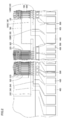
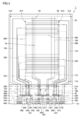
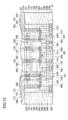
- FIG. 1 is a plan view showing a configuration of an active matrix display device according to Embodiment 1 of the present invention.
- FIG. 4 is a partially enlarged view showing a part of a terminal region in the active matrix display device according to the same embodiment. It is a top view which shows the state in which the disconnection location has arisen in the source wiring of the liquid crystal panel of the active matrix type display apparatus which concerns on the embodiment.
- FIG. 4 is a plan view showing a state in which the liquid crystal panel of the active matrix display device according to the embodiment is irradiated with laser light.
- FIG. 4 is a partial plan view showing a broken portion formed by irradiating a liquid crystal panel of the active matrix display device according to the same embodiment with laser light.
- FIG. 4 is a partially enlarged view showing a part of a terminal region in the active matrix display device according to the same embodiment. It is the elements on larger scale of the VIII part of FIG.
- FIG. 4 is a partial plan view showing a part of a terminal region in the active matrix display device according to the same embodiment.
- FIG. 3 is an enlarged partial plan view showing the configuration of the active matrix display device according to the same embodiment.
- It is a top view which shows the structure of the active matrix type display apparatus which concerns on the modification of this embodiment.
- a liquid crystal panel will be described as an example of a display panel constituting an active matrix display device, but the present invention relates to a microcapsule-type electrophoresis electronic paper, an organic EL (electroluminescence) display, and The present invention can also be applied to a display device other than a liquid crystal panel such as an inorganic EL display.
- FIG. 1 is a plan view showing a configuration of an active matrix display device according to Embodiment 1 of the present invention.
- the wiring formed in the gate electrode layer of the TFT is indicated by a solid line
- the wiring formed in the source / drain electrode layer of the TFT is indicated by a dotted line.
- the inhibition part mentioned later is not formed.
- the active matrix display device 1 includes an active matrix substrate 10 and a counter substrate 20 facing the active matrix substrate 10.
- a liquid crystal material (not shown) is sandwiched between the active matrix substrate 10 and the counter substrate 20.
- the active matrix display device 1 also includes a driver 50 mounted on the active matrix substrate 10, an FPC 40 that is an external substrate electrically connected to the active matrix substrate 10, and a circuit substrate 30.
- the active matrix substrate 10 and the circuit substrate 30 are electrically connected via the FPC 40, but the active matrix display device 1 is connected to the FPC 40 or the circuit substrate 30. May be connected only.
- the counter substrate 20 includes a color filter layer including R (red), G (green), and B (blue) color filters and a black matrix that prevents light leakage between these color filters. Is formed. A common electrode is formed on the color filter layer.
- the active matrix substrate 10 is provided with a display region 60 located substantially at the center of the active matrix substrate 10 and a terminal region 61 where a plurality of input terminals are arranged in the lower part of FIG.
- the terminal region 61 is a region of the active matrix substrate 10 that is not opposed to the counter substrate 20 in a state where the active matrix substrate 10 and the counter substrate 20 are bonded to each other via a liquid crystal material (not shown).
- the active matrix substrate 10 includes a plurality of source lines 100 that are parallel to each other in at least the display region 60, and a plurality of source lines 100 and an insulating film that extend in parallel to each other in the display region 60. A plurality of second wirings that are intersecting with each other are provided.
- the insulating film is made of a material such as SiN x or SiO x .
- FIG. 1 only a part of the plurality of source lines 100 and the plurality of gate lines 200 are illustrated. Note that the numbers of the source wiring 100 and the gate wiring 200 are set as appropriate.
- the plurality of source lines 100 are formed in the display area 60 for each of RGB. That is, in the display region 60, the R source wiring 100, the G source wiring 100, and the B source wiring 100 are formed.
- the present invention is not limited to this in the case of a monochrome liquid crystal panel.
- storage capacitor lines are formed in the display area 60 so as to be parallel to the plurality of gate lines 200.
- switching elements such as TFT or MIM (Metal Insulator Metal) not shown, and pixel electrodes (R, G not shown) connected to the switching elements are provided. Or B) or the like is formed.
- the terminal area 61 is located outside the display area 60 on one end side (the lower side in the drawing) of the plurality of source lines 100.
- a plurality of right source terminals 110 and a plurality of left source terminals 120 which are a plurality of first transmission terminals that respectively send signals from the driver 50 to the plurality of source lines 100 are provided on the display region 60 side in the terminal region 61. Yes.
- the plurality of right source terminals 110 and the plurality of left source terminals 120 are arranged in the extending direction of the plurality of gate wirings 200.
- the driver 50 In order to connect the driver 50 to the terminal area 61, it can be connected by the COG (Chip On Glass) method.
- the driver 50 is provided with a first drive circuit and a second drive circuit that supply signals to the gate wiring 200.
- the first drive circuit is electrically connected to the plurality of second lead lines 250 and supplies a signal to at least a part of the plurality of gate lines 200.
- the second drive circuit is electrically connected to the plurality of third lead lines 260 and supplies signals to at least some of the remaining portions of the plurality of gate lines 200.
- the form of the first drive circuit and the second drive circuit is not limited to this, and at least one may be formed monolithically on the active matrix substrate 10.
- a plurality of right gate terminals 210 and a plurality of left gate terminals 220 which are a plurality of second transmission terminals that respectively send signals from the driver 50 to the plurality of gate lines 200, are provided. It has been.
- the plurality of right gate terminals 210 and the plurality of left gate terminals 220 are arranged in the extending direction of the plurality of gate wirings 200.
- the plurality of right source terminals 110 and the plurality of left source terminals 120 and one end side of the plurality of source wirings 100 are a plurality of right first extraction wirings 170 that are a plurality of first extraction wirings and a plurality of left first extraction wirings. 180 are connected to each other.
- the right source terminal 110 and the left source terminal 120 will be described separately, but the right source terminal 110 and the left source terminal 120 are functionally identical terminals.
- the plurality of right source terminals 110 and the plurality of source wirings 100 are formed with a plurality of right first lead lines so that one right source terminal 110 and one source wiring 100 correspond one-to-one. They are connected by wiring 170.
- the plurality of left source terminals 120 and the plurality of source lines 100 are connected by the plurality of left first lead lines 180 so that one left source terminal 120 and one source line 100 correspond one-to-one. It is connected.
- the plurality of right gate terminals 210 and a part of one end side of the plurality of gate wirings 200 are respectively connected by a plurality of second lead wirings 250.
- the plurality of left gate terminals 220 and the other end side of the remaining portions of the plurality of gate wirings 200 not connected to the plurality of second extraction wirings 250 are respectively connected by a plurality of third extraction wirings 260.
- a part of the plurality of gate wirings 200 and the remaining part of the plurality of gate wirings 200 are alternately formed so as to be parallel to each other.
- the connection configuration of the gate wiring and the lead-out wiring is not limited to that described above.
- a part of the plurality of gate wirings 200 is a gate wiring located in the upper half of the display region 60 and the remaining part of the plurality of gate wirings 200 is used.
- a gate wiring located in the lower half of the display area 60 may be used.
- the plurality of right gate terminals 210 and the plurality of gate wirings 200 are connected by the plurality of second extraction wirings 250 so that one right gate terminal 210 and one gate wiring 200 correspond one-to-one. Yes.
- the plurality of left gate terminals 220 and the plurality of gate wirings 200 are connected by the plurality of third lead wirings 260 so that one left gate terminal 220 and one gate wiring 200 correspond one-to-one. Has been.
- a plurality of output terminals 500 for outputting signals to the driver 50 are provided on the opposite side of the terminal area 61 from the display area 60 side.
- the plurality of output terminals 500 are arranged in the extending direction of the plurality of gate wirings 200.
- a terminal group 400 including a plurality of input terminals 410 to which signals are input from the FPC 40 or the circuit board 30 is provided on the side opposite to the display area 60 when viewed from the plurality of output terminals 500.
- the plurality of input terminals 410 are arranged in the extending direction of the plurality of gate lines 200.
- the terminal group 400 includes a plurality of first common wiring terminals 440, 450, and 460 for inputting signals passing through the plurality of right source terminals 110 and the plurality of left source terminals 120.
- a first common wiring terminal 460 is provided with a plurality of input terminals 410 sandwiched between a first common wiring terminal 440 and a first common wiring terminal 450. ing.
- the terminal group 400 includes a plurality of second common wiring terminals 470 for inputting a signal that passes through the right gate terminal 210 connected to the second lead wiring 250. Further, the terminal group 400 includes a plurality of third common wiring terminals 480 for inputting a signal via the left gate terminal 220 connected to the third lead wiring 260.
- the plurality of first common wiring terminals 440, 450, 460 are connected to the plurality of first common wirings 130, respectively.
- Each of the plurality of first common wirings 130 has a first extending portion 131 that extends so as to separate the plurality of right source terminals 110 and the plurality of left source terminals 120 from the plurality of output terminals 500.
- the plurality of second common wiring terminals 470 are respectively connected to the plurality of second common wirings 230.
- Each of the plurality of second common wirings 230 has a second extending portion 231 that extends so as to separate the plurality of right gate terminals 210 and the plurality of output terminals 500.
- the plurality of third common wiring terminals 480 are connected to the plurality of third common wirings 240, respectively.
- Each of the plurality of third common wirings 240 has a third extending portion 241 that extends so as to separate the plurality of left gate terminals 220 and the plurality of output terminals 500.
- the terminal group 400 includes a plurality of input terminals 410, 420, and 430 connected to the plurality of output terminals 500, respectively.
- FIG. 2 is a partially enlarged view showing a part of the terminal region in the active matrix display device according to the present embodiment.
- first common wires 130 are provided, and one first common wire 130 is provided for each of the plurality of first common wire terminals 440, 450, and 460. Is connected.
- the red pixel common wiring 130R and the first common wiring terminal 440 are connected.
- the green pixel common wiring 130G and the first common wiring terminal 450 are connected.
- the blue pixel common line 130B and the first common line terminal 460 are connected.
- Three second common wirings 230 are provided, and one second common wiring 230 is connected to each of the three second common wiring terminals 470.
- Three third common wires 240 are provided, and one third common wire 240 is connected to each of the three third common wire terminals 480.
- a plurality of first connection wirings that are a plurality of connection wirings between each of the plurality of right source terminals 110 and the plurality of left source terminals 120 and the first extending portions 131 of the plurality of first common wirings 130. 900 is provided. Before the image inspection of the display area 60, the plurality of first connection wirings 900 and the plurality of first common wirings 130 are electrically connected.
- a plurality of second connection wirings 910 that are a plurality of connection wirings are provided between each of the plurality of right gate terminals 210 and the second extending portions 231 of the plurality of second common wirings 230. Before the image inspection of the display area 60, the plurality of second connection wirings 910 and the plurality of second common wirings 230 are electrically connected.
- a plurality of third connection wirings 920 that are a plurality of connection wirings are provided between each of the plurality of left gate terminals 220 and the third extending portions 241 of the plurality of third common wirings 240. Before the image inspection of the display area 60, the plurality of third connection wirings 920 and the plurality of third common wirings 240 are electrically connected.
- three first connection wirings 900 connected to each of the three right source terminals 110 are connected to different first common wirings 130, respectively.
- Three first connection wires 900 connected to each of the three left source terminals 120 are connected to different first common wires 130, respectively.
- the three first common wirings 130 extend from the connected first common wiring terminals 440, 450, and 460 in the extending direction of the plurality of source wirings 100, and then extend to the plurality of gate wirings 200. It changes its direction and extends.
- the three second connection wirings 910 connected to each of the three right gate terminals 210 are connected to different second common wirings 230, respectively.
- Three third connection wirings 920 connected to each of the three left gate terminals 220 are connected to different third common wirings 240, respectively.
- the three second common wirings 230 extend in the extending direction of the plurality of source wirings 100 from each of the three connected second common wiring terminals 470 and then extend in the extending direction of the plurality of gate wirings 200. It changes and extends.
- the three third common wirings 240 extend from the connected third third common wiring terminals 480 in the extending direction of the plurality of source wirings 100 and then extend in the extending direction of the plurality of gate wirings 200. It changes and extends.
- the plurality of right source terminals 110, the plurality of left source terminals 120, and the plurality of output terminals 500 intersect with the second common wiring 230 via an insulating film, and are insulated from the plurality of first connection wirings 900.
- a first spare wiring 700 that intersects with the film is provided.
- the insulating film is made of the same material as the gate insulating film, and is made of a material such as SiN x or SiO x , for example.
- one first spare wiring 700 is provided, and one first spare wiring 700 extends from the second extending portion 231 of one intersecting second common wiring 230. After extending in the extending direction of the plurality of source lines 100, the direction is extended in the extending direction of the plurality of gate lines 200.
- the plurality of source wirings 100 have a plurality of redundant portions 101 that are located on the other end side (upper side in FIG. 1) and outside the display area 60.
- the active matrix substrate 10 crosses any one of the plurality of redundant portions 101 via an insulating film, and is located outside the path that electrically connects the plurality of second lead-out wirings 250 and the second common wiring terminals 470.
- the second auxiliary wiring 710 that can be electrically connected to the second common wiring terminal 470 is formed. That is, the second spare wiring 710 is located outside the plurality of second lead wirings 250 and the first drive circuit in plan view.
- the second spare wiring 710 is connected to one second common wiring 230. Further, the second spare wiring 710 intersects with the redundant portion 101 of all the source wirings 100 through an insulating film.
- the plurality of right source terminals 110 and the plurality of left source terminals 120 and the plurality of output terminals 500 intersect with the third common wiring 240 via an insulating film, and the plurality of first connection wirings 900.
- a third spare wiring 790 that intersects any one of these via an insulating film is provided.
- one third spare wiring 790 is provided, and one third spare wiring 790 is connected to the third extending portion 241 of one intersecting third common wiring 240. After extending in the extending direction of the plurality of source lines 100, the direction is extended in the extending direction of the plurality of gate lines 200.
- the active matrix substrate 10 crosses any one of the plurality of redundant portions 101 via an insulating film, and is positioned outside the path that electrically connects the plurality of third extraction wirings 260 and the third common wiring terminals 480.
- a fourth auxiliary wiring 720 that can be electrically connected to the third common wiring terminal 480 is formed. That is, the fourth preliminary wiring 720 is located outside the plurality of third lead wirings 260 and the second drive circuit in plan view.
- one fourth spare wiring 720 is connected to one third common wiring 240.
- one fourth spare wiring 720 intersects the redundant portion 101 of all the source wirings 100 via an insulating film.
- a storage capacitor wiring 600 is provided so as to surround the display area 60.
- a transfer pad 610 is connected to the auxiliary capacitance wiring 600.
- the common electrode wiring 300 is provided so as to surround the second spare wiring 710 and the fourth spare wiring 720. Common electrode terminals included in the terminal group 400 are connected to the common electrode wiring 300. A transfer pad 310 is further connected to the common electrode wiring 300.
- the transfer pad 310 is connected to a common electrode (not shown) formed on the counter substrate 20. Thereby, a common voltage can be applied to the common electrode formed on the counter substrate 20 from the common electrode terminal.
- the common electrode is not necessarily provided on the counter substrate 20. For example, in a liquid crystal device using a horizontal electric field, the common electrode is provided on the active matrix substrate 10.
- a substrate is manufactured.
- a base substrate for a counter substrate in which a plurality of counter substrate regions to be cut out as a counter substrate 20 is formed by laminating thin films such as a black matrix, a color filter, a conductive film, and an alignment film on a transparent glass substrate.
- a sealing material is applied to one of the base substrates. After the sealing material is applied, both base substrates are bonded to each other.
- Both the bonded base substrates are cut as a mother substrate on which a predetermined number of liquid crystal panels including the active matrix substrate 10 and the counter substrate 20 are formed. That is, the liquid crystal panel shown in FIG. 1 shows one of the liquid crystal panels cut as a mother substrate after the liquid crystal material is injected. Therefore, although not shown, there are other liquid crystal panels on the left and right of the liquid crystal panel of FIG.
- a liquid crystal material is injected into each liquid crystal panel cut as a mother substrate through an injection port formed between the active matrix substrate 10 and the counter substrate 20, for example, by using a vacuum injection method.
- the liquid crystal material may be injected by using a dropping injection method instead of the vacuum injection method.
- the injection port is unnecessary, and the step of sealing the injection port portion is also unnecessary.
- an inspection process for inspecting the electrical connection state of the liquid crystal panel is performed.
- a disconnection, a short circuit, or a defect of the pixel electrode in the active matrix substrate 10 of the liquid crystal panel is inspected.
- an inspection probe is brought into contact with each of the plurality of first common wiring terminals 440, 450, 460, the plurality of second common wiring terminals 470, and the plurality of third common wiring terminals 480, A predetermined voltage is applied.
- the order in which the inspection probes are brought into contact with the plurality of first common wiring terminals 440, 450, 460, the plurality of second common wiring terminals 470, and the plurality of third common wiring terminals 480 is not particularly limited.
- an inspection signal that functions as a scanning signal is input to each of the plurality of gate wirings 200.
- this inspection signal is a signal that turns on the switching element of each pixel for a certain period.
- a test signal that functions as a source signal is input to each of the plurality of source wirings 100.
- This inspection signal is a signal for aligning the liquid crystal in each pixel region in a desired direction.
- the switching element of each pixel is turned on, a test signal that functions as a source signal is input to each pixel electrode, and a common signal is input to the common electrode, whereby a predetermined voltage is applied to the liquid crystal layer.
- irradiation means such as a backlight
- an image is displayed on the display screen of the liquid crystal panel corresponding to the display region 60 of the active matrix substrate 10. It will be displayed.
- the disconnection and short circuit of the wiring in the active matrix substrate 10 of the liquid crystal panel can be inspected, for example, by visual inspection by an inspector.
- an image recognition device may be used, or a detection device that electrically detects disconnection and short-circuiting of the wiring may be used.
- FIG. 3 is a plan view showing a state in which a disconnection portion is generated in the source wiring of the liquid crystal panel of the active matrix display device according to the present embodiment.
- FIG. 4 is a plan view showing a state in which the liquid crystal panel of the active matrix display device according to the present embodiment is irradiated with laser light.
- FIG. 5 is a partial plan view showing a broken portion formed by irradiating the liquid crystal panel of the active matrix display device according to the present embodiment with laser light.
- a repair process is performed in which repair is performed by irradiating a laser beam.
- the laser beam is irradiated with the target 80 as the intersection between the first connection wiring 900 and the third auxiliary wiring 790 that are electrically connected to the source wiring 100 having the disconnection point 70.
- the insulating film in the portion interposed between them is removed, and the third preliminary wiring 790 and the first connection wiring 900 are melt-bonded to form an electric current. Connected.
- the target 80 is irradiated with the laser beam at the intersection of the third auxiliary wiring 790 and the third common wiring 240 electrically connected to the first connection wiring 900.
- the insulating film in the portion interposed between them is removed, and the third preliminary wiring 790 and the third common wiring 240 are fused and electrically connected. Connected to.
- the third common wiring 240 electrically connected to the third spare wiring 790 is connected to the third common wiring terminal 480.
- the laser beam is irradiated with the target 80 as the intersection position of the fourth spare wiring 720 connected to the third common wiring 240 connected to the third common wiring terminal 480 and the redundant portion 101 of the source wiring 100.
- the target 80 By irradiating the target 80 with laser light, the insulating film in the portion interposed between them is removed, and the fourth preliminary wiring 720 and the redundant portion 101 of the source wiring 100 are melt-bonded. Electrically connected.
- the inspection signal input from the third common wiring terminal 480 is applied to one end of the source wiring 100 in the source wiring 100 having the disconnection portion 70. It is sent from both the side and the other end side.
- the signal of the driver 50 input from the left source terminal 120 is sent from both the one end side and the other end side of the source wiring 100 to the source wiring 100 having the disconnection portion 70. become.
- this repair process is not a special additional process because it can be performed in the same process as trimming or blackening, which is a repair process for defective pixels.
- a cutting process for cutting the plurality of first connection wirings 900, the plurality of second connection wirings 910, and the plurality of third connection wirings 920 is performed.
- the cutting process is performed after the repair process.
- the cutting process may be performed before the repair process after the completion of the inspection process.
- a plurality of first connection wirings 900, a plurality of second connection wirings 910, and a plurality of third connection wirings are irradiated by irradiating laser light in the direction indicated by the arrow 90 in FIG. 920 is cut.
- the plurality of right source terminals 110 and the plurality of first common wires 130 are not electrically connected.
- the plurality of left source terminals 120 and the plurality of first common wirings 130 are not electrically connected.
- the plurality of right gate terminals 210 and the plurality of second common wirings 230 are not electrically connected.
- the plurality of left gate terminals 220 and the plurality of third common wirings 240 are not electrically connected.
- each of the plurality of first connection wirings 900 partly interferes with the electrical connection between the plurality of right source terminals 110 and the plurality of left source terminals 120 and the plurality of first common wirings 130. It has the disconnection part 91 which is 1 inhibition part.
- each of the plurality of second connection wirings 910 is in the middle of the disconnection portion 91 that is a second inhibition portion that inhibits electrical connection between the plurality of right gate terminals 210 and the plurality of second common wirings 230.
- Each of the plurality of third connection wirings 920 has a disconnection portion 91 that is a third inhibition portion that inhibits electrical connection between the plurality of left gate terminals 220 and the plurality of third common wirings 240 in the middle.
- the plurality of intersections 901 where the first spare wiring 700 and the plurality of first connection wirings 900 cross each other include the plurality of right source terminals 110 and the plurality of right source terminals 110 and the disconnection portions 91 in each of the plurality of first connection wirings 900.
- the plurality of left source terminals 120 are located.
- the plurality of left source terminals 120 are located.
- a liquid crystal panel is manufactured.
- the method for manufacturing the liquid crystal panel is not limited to the above method.
- a color filter may not be stacked on the counter substrate 20.
- the inspection process and the mounting process may be performed after cutting out each liquid crystal panel.
- the laser in the cutting process since it is not necessary to skip the laser in the cutting process, it can be repaired easily. Further, by effectively using a part of the first connection wiring 900 after cutting as a part of the repair path, it is not necessary to form a path for connecting the input / output terminals to the mounted driver 50. The configuration of the mounted driver 50 can be simplified. Furthermore, by effectively using the common wiring used as the inspection signal input path as a part of the repair path, the area where the repair path is arranged can be prevented from becoming large.
- a repair path is configured using the third spare wiring 790 and the fourth spare wiring 720. Therefore, the third lead wiring 260 and the repair path do not intersect. Therefore, it is possible to reduce the load capacity of the repair path and reduce the delay of the signal flowing through the repair path.
- first spare wiring 700 and the second spare wiring 710 may be used as the repair path depending on the position of the source wiring 100 having the disconnection portion.
- the first connection wiring 900 connected to the source wiring 100 having the disconnection portion among the plurality of source wirings 100 is mutually connected to the first spare wiring 700 intersecting the first connection wiring 900.
- the insulating film in the portion interposed between the two is removed and electrically connected.
- the first auxiliary wiring 700 electrically connected to the first connection wiring 900 is removed from the second common wiring 230 intersecting with the first auxiliary wiring 700 and the insulating film in the portion interposed therebetween. To be electrically connected.
- the second common wiring terminal 470 connected to the second common wiring 230 electrically connected to the first spare wiring 700 is electrically connected to the second spare wiring 710.
- the second auxiliary wiring 710 that is electrically connected to the second common wiring terminal 470 is electrically removed by removing any of the plurality of redundant portions 101 and the insulating film interposed between them. Connected.
- the signal of the driver 50 input from the right source terminal 110 is sourced to the source wiring 100 electrically connected to the first connection wiring 900 connected to the first spare wiring 700. It is sent from both one end side and the other end side of the wiring 100.
- the second lead wiring 250 and the repair route do not intersect. Therefore, it is possible to reduce the load capacity of the repair path and reduce the delay of the signal flowing through the repair path.
- the disconnection portion 91 is provided as the inhibition portion.
- the configuration of the inhibition portion is not limited to this, and for example, a switching element connected to the first connection wiring 900 may be used as the inhibition portion.
- first spare wiring 700 and the third spare wiring 790 are provided in the mounting area in which the driver 50 is mounted in the terminal area 61, a space for providing the first spare wiring 700 and the third spare wiring 790 is provided. It is not necessary to ensure separately, and it can suppress that a liquid crystal panel enlarges.
- the active matrix display device 1 may have a configuration in which the source wiring 100 and the gate wiring 200 are interchanged with each other.
- both the second lead wiring 250 and the third lead wiring 260 are provided, but only one of them may be provided.
- the three first common wirings 130 are provided, but it is sufficient that one or more first common wirings 130 are provided.
- one first spare wiring 700 is provided. However, one or more first spare wirings 700 may be provided, and the number of first spare wirings 700 may be set to the first common wirings 130. The number may be the same.
- the second spare wiring 710 and the second common wiring 230 are connected. However, even if the second spare wiring 710 and the second common wiring 230 intersect with each other through an insulating film. Good.
- the laser beam is irradiated using the intersection position of the second auxiliary wiring 710 and the second common wiring 230 as the target 80. By irradiating the target 80 with laser light, the insulating film in the portion interposed between them is removed, and the second preliminary wiring 710 and the second common wiring 230 are fused and electrically connected. Connected to. Even in this way, repair can be performed.
- a plurality of lead-out lines on the active matrix substrate 10 are divided into a gate layer and a source / drain layer with an insulating film interposed therebetween. Therefore, compared with the case where all the wirings are formed on the same layer, the interval between the adjacent lead wirings in a plan view can be narrowed. Therefore, since the arrangement area of the lead-out wiring in the active matrix substrate 10 can be reduced, the active matrix display device 1 can be downsized.
- the present invention can also be used for purposes other than disconnection repair.
- it can be used for wiring resistance management and defect analysis in the panel manufacturing process.
- When measuring wiring resistance and checking the driver output signal easily measure the wiring resistance or driver output signal by contacting the probe to the common wiring terminal with a specific wiring connected to the spare wiring. Can do.
- the active matrix display device is not limited to the one that has undergone the repair process, but includes those that have not undergone the repair process.
- an active matrix display device according to Embodiment 2 of the present invention will be described. Note that the active matrix display device 2 according to the present embodiment is different from the active matrix display device 1 according to the first embodiment only in the number of spare wirings, and therefore, description of other configurations will not be repeated.
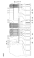
- FIG. 6 is a plan view showing a configuration of an active matrix display device according to Embodiment 2 of the present invention.
- FIG. 7 is a partially enlarged view showing a part of the terminal region in the active matrix display device according to the present embodiment.
- FIG. 8 is a partially enlarged view of the VIII portion in FIG.
- FIG. 9 is a partial plan view showing a part of the terminal region in the active matrix display device according to the present embodiment.
- FIG. 6 shows a state before the first, second, and third inhibition portions are formed.
- the first, second, and third inhibition portions are formed at the same positions as in the active matrix display device 1 according to the first embodiment.
- one first spare line and one second spare line are provided, and the third spare line and the fourth spare line are provided.
- Two spare wirings are provided for each.
- left third spare wiring 791 located on the left side and right third spare wiring 792 located on the right side are provided as the third spare wiring.
- the left third spare wiring 791 intersects the third common wiring 240 of the three third common wirings 240 in which the third extending portion 241 is located at the uppermost position via an insulating film.
- the right third spare wiring 792 intersects the third common wiring 240 of which the third extending portion 241 is located in the middle among the three third common wirings 240 via an insulating film.
- a left fourth spare wiring 721 located on the left side and a right fourth spare wiring 722 located on the right side are provided.
- the left fourth spare wiring 721 is connected to the third common wiring 240 in which the third extending portion 241 is located at the uppermost position among the three third common wirings 240.
- the right fourth spare wiring 722 is connected to the third common wiring 240 in which the third extending portion 241 is located in the middle among the three third common wirings 240.
- the third common line in which the right fourth spare line 722 is connected to the left fourth spare line 721 to connect the right fourth spare line 722 and the third common line 240 is formed so as to straddle the third extension portion 241 of 240.
- the right fourth spare wiring 722 is connected to the TFT source from the gate electrode layer of the TFT by contact holes 723 and 724 formed so as to sandwich the third extending portion 241 of the third common wiring 240 therebetween. / It is again disposed on the gate electrode layer of the TFT via the drain electrode layer.
- the length of the third extension 241 of the third common wiring 240 connected to the left fourth spare wiring 721 is set to the length of the third extension of the third common wiring 240 connected to the right fourth spare wiring 722. It is substantially the same as the length of 241.
- the third extension line 241 of the third common line 240 connected to the left side fourth spare line 721 and the right side third spare line 792 do not intersect with the right side third spare line 792.
- the third common wiring 240 can be connected.
- the source wiring 100 can be repaired more than in the active matrix display device 1 according to the first embodiment, and the load capacity of the repair path can be reduced to reduce the delay of the signal flowing through the repair path. can do.
- an active matrix display device according to Embodiment 3 of the present invention will be described. Note that the active matrix display device 3 according to the present embodiment is different from the active matrix display device 1 according to the first embodiment only in the arrangement of the spare wirings, and therefore, description of other configurations will not be repeated.
- FIG. 10 is a plan view showing a configuration of an active matrix display device according to Embodiment 3 of the present invention.
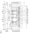
- FIG. 11 is an enlarged partial plan view showing the configuration of the active matrix display device according to the present embodiment.
- the wiring formed in the gate electrode layer of the TFT is indicated by a solid line, and the wiring formed in the source / drain electrode layer of the TFT is indicated by a dotted line.
- 10 and 11 show a state before the first, second, and third inhibition portions are formed.
- the first, second, and third inhibition portions are formed at the same positions as in the active matrix display device 1 according to the first embodiment.
- a plurality of source lines 100 are divided into two groups. Specifically, a right source line group 102 located on the right side and a left source line group 103 located on the left side are provided.
- the plurality of source lines 100 included in the right source line group 102 are connected to the plurality of right first lead lines 170, respectively.
- the plurality of right first lead wires 170 are respectively connected to the plurality of right source terminals 110.
- the plurality of source lines 100 included in the left source line group 103 are connected to the plurality of left first lead lines 180, respectively.
- the plurality of left first lead wires 180 are connected to the plurality of left source terminals 120, respectively.
- the plurality of first connection wirings 900 include a right first connection wiring group 902 located on the right side and a left first connection wiring group 903 located on the left side.
- the first spare wiring 730 extends from the second extending portion 231 of the intersecting second common wiring 230 in the extending direction of the plurality of source wirings 100 and then is directed in the extending direction of the plurality of gate wirings 200. It changes and extends.
- the third spare wiring 740 extends in the extending direction of the plurality of source wirings 100 from the third extending portion 241 of the intersecting third common wiring 240 and then is directed in the extending direction of the plurality of gate wirings 200. It changes and extends.
- the first spare wiring 730 intersects only with the right first connection wiring group 902. That is, the first spare wiring 730 does not intersect the left first connection wiring group 903.
- the third spare wiring 740 intersects only with the left first connection wiring group 903. That is, the third spare wiring 740 does not intersect the right first connection wiring group 902.
- the second spare wiring 760 intersects only the plurality of source wirings 100 included in the right source wiring group 102 in the redundant portion 101.
- the fourth spare wiring 770 intersects only the plurality of source wirings 100 included in the left source wiring group 103 in the redundant portion 101.
- the second spare wiring 760 and the fourth spare wiring 770 intersect with each of the plurality of redundant portions 101 through the insulating film so as not to overlap each other.
- the number of intersections 901 between the first spare wiring 700 and the plurality of first connection wirings 900 can be reduced.
- the number of intersections 904 between the third spare wiring 740 and the plurality of first connection wirings 900 can be reduced.
- the number of intersections between the second spare wiring 760 and the fourth spare wiring 770 and the plurality of source wirings 100 can be reduced. As a result, the load capacity of the repair path can be reduced, and the delay of the signal flowing through the repair path can be reduced.
- this embodiment Compared to the case where the second spare wiring 710 and the fourth spare wiring 720 intersect the redundant portions 101 of all the source wirings 100 as in the active matrix display device 1 according to the first embodiment, this embodiment In the embodiment, a wiring formation region can be reduced. As a result, the outer shape of the panel can be reduced, and a wide laser irradiation area in the cutting process can be secured.
- FIG. 12 is a plan view showing a configuration of an active matrix display device according to a modification of the present embodiment.
- FIG. 13 is an enlarged partial plan view showing the configuration of the active matrix display device according to this modification.
- the wiring formed in the gate electrode layer of the TFT is indicated by a solid line, and the wiring formed in the source / drain electrode layer of the TFT is indicated by a dotted line.
- 12 and 13 show a state before the first, second, and third inhibition portions are formed.
- the first, second, and third inhibition portions are formed at the same positions as in the active matrix display device 3 according to the first embodiment.
- the active matrix display device 3a according to the present modification is different from the active matrix display device 3 according to the third embodiment in terms of the number of spare wirings, description of other configurations will not be repeated.
- the right first spare wiring 731 located on the right side, the left first spare wiring 733 located on the left side, and the right first spare wiring 731 and the left first spare wiring 733 are arranged.
- a middle first auxiliary wiring 732 located between them is provided.
- the right first spare wiring 731, the left first spare wiring 733, and the middle first spare wiring 732 are a plurality of source wirings 100 from each of the second extending portions 231 of the three intersecting second common wirings 230. After extending in the extending direction, the direction of the plurality of gate wirings 200 is changed in the extending direction.
- the right first spare wiring 731, the left first spare wiring 733, and the middle first spare wiring 732 intersect only the right first connection wiring group 902. That is, the right first spare wiring 731, the left first spare wiring 733, and the middle first spare wiring 732 do not intersect the left first connection wiring group 903.
- the lengths of the second extending portions 231 of the three second common wires 230 are substantially the same.
- the right first spare wiring 731, the right first spare wiring 733, and the middle first spare wiring 732 can each intersect with only one second common wiring 230 via an insulating film. it can.
- the right first spare wiring 731, the right first spare wiring 733, and the middle first spare wiring are located at positions where the ends of the second extending portions 231 of the three second common wirings 230 are shifted. 732 cross each other.
- the third spare wiring As the third spare wiring, the left third spare wiring 741 located on the left side, the right third spare wiring 743 located on the right side, and the middle located between the left third spare wiring 741 and the right first spare wiring 743 A side third auxiliary wiring 742 is provided.
- the left third spare wiring 741, the right third spare wiring 743, and the middle third spare wiring 742 are a plurality of source wirings 100 from each of the third extending portions 241 of the three third common wirings 240 that intersect. After extending in the extending direction, the direction of the plurality of gate wirings 200 is changed in the extending direction.
- the left third spare wiring 741, the right third spare wiring 743, and the middle third spare wiring 742 intersect only the left first connection wiring group 903. That is, the left third spare wiring 741, the right third spare wiring 743, and the middle third spare wiring 742 do not intersect the right first connection wiring group 902.
- the lengths of the third extending portions 241 of the three third common wires 240 are substantially the same. In this way, the left third spare wiring 741, the right third spare wiring 743, and the middle third spare wiring 742 can each intersect with only one third common wiring 240 via the insulating film. it can.
- the left third spare wiring 741, the right third spare wiring 743, and the middle third spare wiring are arranged at positions where the ends of the third extending portions 241 of the three third common wirings 240 are shifted from each other. 742 is crossed.
- the right second spare wiring 761 located on the right side As the second spare wiring, the right second spare wiring 761 located on the right side, the left second spare wiring 763 located on the left side, and the middle located between the right second spare wiring 761 and the left second spare wiring 763.
- a side second auxiliary wiring 762 is provided.
- the right second spare wiring 761, the left second spare wiring 763, and the middle second spare wiring 762 are each connected to only one of the three second common wirings 230.
- the connection form is the contact hole connection described in the second embodiment.
- the right second spare wiring 761, the left second spare wiring 763, and the middle second spare wiring 762 cross only the plurality of source wirings 100 included in the right source wiring group 102 in the redundant portion 101.
- a side fourth auxiliary wiring 772 is provided.
- the left fourth spare wiring 771, the right fourth spare wiring 773, and the middle fourth spare wiring 772 are each connected to only one of the three third common wirings 240.
- the connection form is the contact hole connection described in the second embodiment.
- the left fourth spare wiring 771, the right fourth spare wiring 773, and the middle fourth spare wiring 772 intersect only the plurality of source wirings 100 included in the left source wiring group 103 in the redundant portion 101.
- the redundant portions 101 intersect with each other via an insulating film so as not to overlap.
- the source wiring 100 can be repaired more than the active matrix display device 3 according to the third embodiment.
- the active matrix display device 4 according to the present embodiment is different from the active matrix display device 1 according to the first embodiment only in that the gate wiring can be repaired. Therefore, the description of the other configurations will not be repeated.
- FIG. 14 is a plan view showing a configuration of an active matrix display device according to Embodiment 4 of the present invention.
- the wiring formed in the gate electrode layer of the TFT is indicated by a solid line
- the wiring formed in the source / drain electrode layer of the TFT is indicated by a dotted line.
- the active matrix display device 4 includes an active matrix substrate 1010 and a counter substrate 1020 facing the active matrix substrate 1010.
- a liquid crystal material (not shown) is sandwiched between the active matrix substrate 1010 and the counter substrate 1020.
- the active matrix display device 4 includes a driver 1050 mounted on the active matrix substrate 1010, an FPC 1040 that is an external substrate electrically connected to the active matrix substrate 1010, and a circuit substrate 1030.
- the active matrix substrate 1010 and the circuit substrate 1030 are electrically connected via the FPC 1040, but the active matrix substrate 1010 is connected only to the FPC 1040 or the circuit substrate 1030. May be.
- the active matrix substrate 1010 is provided with a display region 1060 located substantially in the center of the active matrix substrate 1010 and a terminal region 1061 located on the right side in FIG.
- the terminal region 1061 is a region of the active matrix substrate 1010 that is not opposed to the counter substrate 1020 in a state where the active matrix substrate 1010 and the counter substrate 1020 are bonded to each other via a liquid crystal material (not shown).
- the active matrix substrate 1010 includes a gate wiring 1100 which is a plurality of first wirings extending in parallel to each other at least in the display region 1060 and a plurality of gate wirings 1100 and an insulating film extending in parallel to each other in the display region 1060.
- a plurality of source lines 1200 that are a plurality of second lines crossing each other are provided.
- the insulating film is made of a material such as SiN x or SiO x .
- FIG. 14 shows only a part of the plurality of gate wirings 1100 and the plurality of source wirings 1200. Note that the number of each of the gate wiring 1100 and the source wiring 1200 is set as appropriate.
- storage capacitor lines are formed in the display area 1060 so as to be parallel to the plurality of gate lines 1100.
- a switching element such as a TFT or MIM (Metal Insulator Metal) not shown, and a pixel electrode (R, G not shown) connected to the switching element are provided. Or B) or the like is formed.
- the terminal area 1061 is located outside the display area 1060 on one end side (right side in the drawing) of the plurality of gate wirings 1100.
- a plurality of upper gate terminals 1110 and a plurality of lower gate terminals 1120 which are a plurality of first transmission terminals that respectively send signals from the driver 1050 to the plurality of gate wirings 1100 are provided on the display region 1060 side in the terminal region 1061. ing.
- the plurality of upper gate terminals 1110 and the plurality of lower gate terminals 1120 are arranged in the extending direction of the plurality of source lines 1200.
- the driver 1050 In order to connect the driver 1050 to the terminal area 1061, it can be connected by a COG (Chip On Glass) method.
- the driver 1050 is provided with a first drive circuit and a second drive circuit that supply a signal to the source wiring 1200.
- the first drive circuit is electrically connected to the plurality of second lead wirings 1250 and supplies a signal to at least a part of the plurality of source wirings 1200.
- the second drive circuit is electrically connected to the plurality of third lead wirings 1260 and supplies a signal to at least some of the remaining portions of the plurality of source wirings 1200.
- the form of the first drive circuit and the second drive circuit is not limited to this, and at least one of them may be formed monolithically on the active matrix substrate 1010.
- a plurality of upper source terminals 1210 and a plurality of lower source terminals 1220 which are a plurality of second transmission terminals that respectively send signals from the driver 1050 to the plurality of source wirings 1200 are provided on the display region 1060 side in the terminal region 1061. Is provided.
- the plurality of upper source terminals 1210 and the plurality of lower source terminals 1220 are arranged in the extending direction of the plurality of source lines 1200.
- the plurality of upper gate terminals 1110 and the plurality of lower gate terminals 1120 and the one end side of the plurality of gate wirings 1100 are a plurality of upper first extraction wirings 1170 and a plurality of lower first ones which are a plurality of first extraction wirings. They are connected to each other by a lead wiring 1180.
- the upper gate terminal 1110 and the lower gate terminal 1120 will be described separately, but the upper gate terminal 1110 and the lower gate terminal 1120 are functionally identical terminals.
- the plurality of upper gate terminals 1110 and the plurality of gate wirings 1100 have a plurality of upper first lead lines so that one upper gate terminal 1110 and one gate wiring 1100 have a one-to-one correspondence. They are connected by wiring 1170.
- a plurality of lower gate terminals 1120 and a plurality of gate wirings 1100 include a plurality of lower first lead lines so that one lower gate terminal 1120 and one gate wiring 1100 correspond one-to-one. They are connected by wiring 1180.
- the plurality of upper source terminals 1210 and one end side of a part of the plurality of source wirings 1200 are respectively connected by a plurality of second extraction wirings 1250.
- the plurality of lower source terminals 1220 and the other ends of the remaining portions of the plurality of source wirings 1200 that are not connected to the plurality of second extraction wirings 1250 are respectively connected by a plurality of third extraction wirings 1260.
- a part of the plurality of source wirings 1200 and the remaining part of the plurality of source wirings 1200 are alternately formed so as to be parallel to each other.
- the connection configuration of the gate wiring and the lead wiring is not limited to the above, and for example, a part of the plurality of source wirings 1200 is a source wiring located in the left half of the display region 1060 and the remaining part of the plurality of source wirings 1200 is used.
- the source wiring may be located in the right half of the display area 1060.
- a plurality of upper source terminals 1210 and a plurality of source wirings 1200 are connected by a plurality of second extraction wirings 1250 so that one upper source terminal 1210 and one source wiring 1200 correspond one-to-one. Yes.
- the plurality of lower source terminals 1220 and the plurality of source wirings 1200 include a plurality of third extraction wirings 1260 so that one lower source terminal 1220 and one source wiring 1200 correspond one-to-one. Connected by.
- a plurality of output terminals 1500 for outputting signals to the driver 1050 are provided on the side opposite to the display area 1060 side in the terminal area 1061.
- the plurality of output terminals 1500 are arranged in the extending direction of the plurality of source lines 1200.
- a terminal group 1400 including a plurality of input terminals 1410 to which signals are input from the FPC 1040 or the circuit board 1030 is provided on the side opposite to the display area 1060 side when viewed from the plurality of output terminals 1500.
- the plurality of input terminals 1410 are arranged in the extending direction of the plurality of source lines 1200.
- the terminal group 1400 includes a plurality of first common wiring terminals 1440, 1450, and 1460 for inputting signals that pass through the plurality of upper gate terminals 1110 and the plurality of lower gate terminals 1120.
- a first common wiring terminal 1460 is provided with a plurality of input terminals 1410 sandwiched between the first common wiring terminal 1440 and the first common wiring terminal 1450. ing.
- the terminal group 1400 includes a plurality of second common wiring terminals 1470 for inputting a signal that passes through the upper source terminal 1210 connected to the second lead wiring 1250. Further, the terminal group 1400 includes a plurality of third common wiring terminals 1480 for inputting a signal that passes through the lower source terminal 1220 connected to the third lead wiring 1260.
- the plurality of first common wiring terminals 1440, 1450, and 1460 are connected to the plurality of first common wirings 1130, respectively.
- Each of the plurality of first common wirings 1130 has a first extending portion 1131 that extends so as to separate the plurality of upper gate terminals 1110 and the plurality of lower gate terminals 1120 from the plurality of output terminals 1500. .
- the plurality of second common wiring terminals 1470 are connected to the plurality of second common wirings 1230, respectively.
- Each of the plurality of second common wirings 1230 has a second extending portion 1231 extending so as to divide between the plurality of upper source terminals 1210 and the plurality of output terminals 1500.
- the plurality of third common wiring terminals 1480 are connected to the plurality of third common wirings 1240, respectively.
- Each of the plurality of third common wirings 1240 has a third extending portion 1241 that extends so as to separate the plurality of lower source terminals 1220 and the plurality of output terminals 1500 from each other.
- the terminal group 1400 includes a plurality of input terminals 1410, 1420, and 1430 connected to the plurality of output terminals 1500, respectively.
- first common wirings 1130 are provided, and one first common wiring 1130 is connected to each of the plurality of first common wiring terminals 1440, 1450, and 1460.
- Three second common wires 1230 are provided, and one second common wire 1230 is connected to each of the three second common wire terminals 1470.
- Three third common wires 1240 are provided, and one third common wire 1240 is connected to each of the three third common wire terminals 1480.
- a plurality of first connection wirings that are a plurality of connection wirings.
- a wiring 1900 is provided. Before the image inspection of the display area 1060, the plurality of first connection wirings 1900 and the plurality of first common wirings 1130 are electrically connected.
- a plurality of second connection wirings 1910 that are a plurality of connection wirings are provided between each of the plurality of upper source terminals 1210 and the second extending portion 1231 of the plurality of second common wirings 1230. Before the image inspection of the display area 1060, the plurality of second connection wirings 1910 and the plurality of second common wirings 1230 are electrically connected.
- a plurality of third connection wirings 1920 that are a plurality of connection wirings are provided between each of the plurality of lower source terminals 1220 and the third extending portion 1241 of the plurality of third common wirings 1240. . Before the image inspection of the display area 1060, the plurality of third connection wirings 1920 and the plurality of third common wirings 1240 are electrically connected.
- three first connection wirings 1900 connected to each of the three upper gate terminals 1110 are connected to different first common wirings 1130, respectively.
- Three first connection wirings 1900 connected to each of the three lower gate terminals 1120 are connected to different first common wirings 1130, respectively.
- the three first common wirings 1130 extend from the connected first common wiring terminals 1440, 1450, and 1460 in the extending direction of the plurality of gate wirings 1100, and then extend to the plurality of source wirings 1200. It changes its direction and extends.
- the three second connection wirings 1910 connected to each of the three upper source terminals 1210 are connected to different second common wirings 1230, respectively.
- Three third connection wirings 1920 connected to each of the three lower source terminals 1220 are connected to different third common wirings 1240, respectively.
- the three second common wirings 1230 extend from the connected second common wiring terminals 1470 in the extending direction of the plurality of gate wirings 1100 and then extend in the extending direction of the plurality of source wirings 1200. It changes and extends.
- the three third common wirings 1240 extend from the connected third common wiring terminals 1480 in the extending direction of the plurality of gate wirings 1100 and then extend in the extending direction of the plurality of source wirings 1200. It changes and extends.
- the second common wiring 1230 intersects with the insulating film, and the plurality of first connection wirings 1900
- a first spare wiring 1700 that intersects with the insulating film interposed therebetween is provided.
- the insulating film is made of the same material as the gate insulating film, and is made of a material such as SiN x or SiO x , for example.
- one first spare wiring 1700 is provided, and one first spare wiring 1700 extends from the second extension portion 1231 of one intersecting second common wiring 1230. After extending in the extending direction of the plurality of gate wirings 1100, the direction is extended in the extending direction of the plurality of source wirings 1200.
- the plurality of gate wirings 1100 have a plurality of redundant portions 1101 positioned on the outer side of the display area 1060 on the other end side (left side in FIG. 14).
- the active matrix substrate 1010 intersects with any of the plurality of redundant portions 1101 via an insulating film, and is positioned outside the path that electrically connects the plurality of second lead wirings 1250 and the second common wiring terminals 1470.
- a second auxiliary wiring 1710 that can be electrically connected to the second common wiring terminal 1470 is formed. That is, the second auxiliary wiring 1710 is located outside the plurality of second lead wirings 1250 and the first drive circuit in plan view.
- the second spare wiring 1710 is connected to one second common wiring 1230. Further, the second spare wiring 1710 intersects with the redundant portion 1101 of all the gate wirings 1100 via an insulating film.
- the plurality of upper gate terminals 1110 and the plurality of lower gate terminals 1120 and the plurality of output terminals 1500 intersect with the third common wiring 1240 via an insulating film, and the plurality of first connection wirings.
- a third spare wiring 1790 that intersects any of 1900 with an insulating film interposed therebetween is provided.
- one third spare line 1790 is provided, and one third spare line 1790 is provided from the third extending portion 1241 of one intersecting third common line 1240. After extending in the extending direction of the plurality of gate wirings 1100, the direction is extended in the extending direction of the plurality of source wirings 1200.
- the active matrix substrate 1010 crosses any of the plurality of redundant portions 1101 via an insulating film, and is positioned outside the path that electrically connects the plurality of third extraction wirings 1260 and the third common wiring terminals 1480.
- a fourth auxiliary wiring 1720 that can be electrically connected to the third common wiring terminal 1480 is formed. That is, the fourth preliminary wiring 1720 is located outside the plurality of third lead wirings 1260 and the second drive circuit in plan view.
- one fourth spare wiring 1720 is connected to one third common wiring 1240.
- one fourth spare wiring 1720 intersects with the redundant portion 1101 of all the gate wirings 1100 via an insulating film.
- a storage capacitor line 1600 is provided so as to surround the display area 1060.
- a transfer pad 1610 is connected to the auxiliary capacity wiring 1600.
- a common electrode wiring 1300 is provided so as to surround the second spare wiring 1710 and the fourth spare wiring 1720.
- Common electrode terminals included in the terminal group 1400 are connected to the common electrode wiring 1300.
- a transfer pad 1310 is further connected to the common electrode wiring 1300.
- the transfer pad 1310 is connected to a common electrode (not shown) formed on the counter substrate 1020. Accordingly, a common voltage can be applied to the common electrode formed on the counter substrate 1020 from the common electrode terminal.
- the common electrode is not necessarily provided on the counter substrate 1020. For example, in a liquid crystal device using a horizontal electric field, the common electrode is provided on the active matrix substrate 1010.
- the first connection wiring 1900, the second connection wiring 1910, and the third connection wiring 1920 are irradiated with the laser light, which is a hindrance. Forming part.
- a plurality of intersections 1901 where the first spare wiring 1700 and the plurality of first connection wirings 1900 intersect each other are a plurality of upper sides than the disconnection portions formed in each of the plurality of first connection wirings 1900. It is located on the gate terminal 1110 and the plurality of lower gate terminals 1120 side.
- a plurality of intersections 1904 at which the third spare wiring 1790 and the plurality of first connection wirings 1900 intersect each other are a plurality of upper gate terminals 1110 than a disconnection portion formed in each of the plurality of first connection wirings 1900. And located on the plurality of lower gate terminals 1120 side.
- the gate wiring 1100 can be repaired.
- a driver 1050 may be mounted on the signal input side of the gate wiring 1100 as in this embodiment. Even in such a configuration, the present invention is applicable.
Landscapes
- Physics & Mathematics (AREA)
- Nonlinear Science (AREA)
- Chemical & Material Sciences (AREA)
- Crystallography & Structural Chemistry (AREA)
- General Physics & Mathematics (AREA)
- Optics & Photonics (AREA)
- Mathematical Physics (AREA)
- Engineering & Computer Science (AREA)
- Microelectronics & Electronic Packaging (AREA)
- Liquid Crystal (AREA)
- Devices For Indicating Variable Information By Combining Individual Elements (AREA)
Abstract
アクティブマトリクス型表示装置においては、第2共通配線(230)と絶縁膜を介して交差し、かつ、複数の第1接続用配線(900)のいずれかと絶縁膜を介して交差する第1予備配線(700)と、複数のソース配線(100)の各々の他端側の部分であって表示領域(60)の外側に位置する複数の冗長部(101)のいずれかと絶縁膜を介して交差し、平面視において複数の第2引出配線(250)および第1駆動回路の外側に位置して、第2共通配線(230)と電気的に接続可能な第2予備配線(710)とを有する。第1予備配線(700)と複数の第1接続用配線(900)とが交差している複数の交差部(901)は、複数の第1接続用配線(900)の各々において第1阻害部より複数のソース端子(110,120)側に位置している。
Description
本発明は、アクティブマトリクス型表示装置に関する。
アクティブマトリクス型表示装置である液晶表示装置において、予備配線を備えた装置を開示した先行文献として特開2003-222895号公報(特許文献1)および特開2005-249993号公報(特許文献2)がある。
特許文献1に記載された液晶表示装置は、TFT(thin film transistor)アレイ基板上において、IC(integrated circuit)の実装部における入出力端子間を通過する、表示領域の欠陥を修正するための予備配線を備えている。また、アクティブマトリクス素子を駆動するICの内部を通して電気的に接続される入力側端子と出力側端子とからなるスルー端子が設けられている。さらに、予備配線がスルー端子の出力側に接続され、画像検査時に使用するRGBごとに接続された一括点画ラインがスルー端子の入力側に接続されている。
アクティブマトリクス素子を駆動するIC実装前に、レーザなどにより一括点画ラインは切断される。アクティブマトリクス素子を駆動するIC実装後においては、スルー端子に接続された配線のみによって回路が構成されている。
特許文献2に記載されたアクティブマトリクス型表示装置においては、TFTへの入力配線とFPC(Flexible Printed Circuits)基板側の配線とを接続する端子間ショート用配線をレーザ照射により切断している。断線不良箇所を有するTFTへの入力配線がある場合には、切断した端子間ショート用配線を金属錯体で修正することにより、または、レーザスキップして一部の入力端子間ショート用配線を除いて他の入力端子間ショート用配線を切断することによりリペアしている。
特許文献1に記載された液晶表示装置においては、実装されるICなどのドライバに、スルー端子に対応した経路および端子を形成する必要がある。特許文献2に記載されたアクティブマトリクス型表示装置においては、リペアする際にレーザスキップまたは金属錯体を用いた修正が必要となり、複雑なリペア方法が必要である。また、アクティブマトリクス基板の外部に予備配線を設けた場合には、製造コストの観点から問題がある。
本発明は上記の問題点に鑑みてなされたものであって、廉価に作製して簡易にリペアすることができるとともに、実装されるドライバの構成を簡略化できる、アクティブマトリクス型表示装置を提供することを目的とする。
本発明に基づくアクティブマトリクス型表示装置は、アクティブマトリクス基板と、アクティブマトリクス基板に実装されるドライバと、アクティブマトリクス基板に電気的に接続される外部基板とを備える。アクティブマトリクス基板は、少なくとも表示領域において互いに平行に延在する複数の第1配線と、表示領域において互いに平行に延在し、複数の第1配線と絶縁膜を介して交差する複数の第2配線とを有する。また、アクティブマトリクス基板は、複数の第1配線の一端側の表示領域の外側に位置する端子領域内の表示領域側に位置し、複数の第2配線の延在方向に並び、ドライバからの信号を複数の第1配線にそれぞれ送る複数の第1送信端子と、複数の第1配線の一端側の表示領域の外側に位置する端子領域内の表示領域側に位置し、複数の第2配線の延在方向に並び、ドライバからの信号を複数の第2配線にそれぞれ送る複数の第2送信端子とを有する。さらに、アクティブマトリクス基板は、複数の第1配線の一端側と複数の第1送信端子とをそれぞれ接続する複数の第1引出配線と、複数の第2配線の少なくとも一部の一端側とこの一端側に位置する前記第2送信端子とをそれぞれ接続する複数の第2引出配線とを有する。また、アクティブマトリクス基板は、複数の第2引出配線に電気的に接続され、複数の第2配線の少なくとも一部に信号を供給する第1駆動回路と、端子領域内の表示領域側とは反対側に位置し、ドライバに対して信号を出力する複数の出力端子とを有する。さらに、アクティブマトリクス基板は、端子領域内において複数の出力端子から見て表示領域側とは反対側に位置し、外部基板から信号が入力される複数の入力端子を含む端子群を有する。また、アクティブマトリクス基板は、端子群に含まれ、複数の第1送信端子を経由する信号を入力するための第1共通配線用端子と、端子群に含まれ、第2引出配線に接続された複数の第2送信端子を経由する信号を入力するための第2共通配線用端子とを有する。さらに、第1共通配線用端子と接続され、複数の第1送信端子と複数の出力端子との間を区切るように延在する第1延在部を有する第1共通配線と、第2共通配線用端子と接続され、第2引出配線に接続された複数の第2送信端子と前記複数の出力端子との間を区切るように延在する第2延在部を有する第2共通配線とを有する。また、アクティブマトリクス基板は、複数の第1送信端子の各々と第1共通配線の第1延在部との間に設けられた複数の第1接続用配線と、第2引出配線に接続された複数の第2送信端子の各々と第2共通配線の第2延在部との間に設けられた複数の第2接続用配線とを有する。さらに、アクティブマトリクス基板は、第2共通配線と絶縁膜を介して交差し、かつ、複数の第1接続用配線のいずれかと絶縁膜を介して交差する第1予備配線と、複数の第1配線の各々の他端側の部分であって表示領域の外側に位置する複数の冗長部のいずれかと絶縁膜を介して交差し、平面視において複数の第2引出配線および第1駆動回路の外側に位置して、第2共通配線と電気的に接続可能な第2予備配線とを有する。また、アクティブマトリクス基板は、複数の第1接続用配線の各々は途中に、複数の第1送信端子と第1共通配線との間の電気的接続を阻害する第1阻害部を有し、複数の第2接続用配線の各々は途中に、第2引出配線に接続された複数の第2送信端子と第2共通配線との間の電気的接続を阻害する第2阻害部を有する。第1予備配線と複数の第1接続用配線とが交差している複数の交差部は、複数の第1接続用配線の各々において第1阻害部より複数の第1送信端子側に位置している。
本発明の一形態においては、アクティブマトリクス基板は、複数の第2引出配線に接続されていない複数の第2配線の残部の少なくとも一部の他端側に接続された複数の第3引出配線と、複数の第3引出配線に電気的に接続され、複数の第2配線の残部の少なくとも一部に信号を供給する第2駆動回路とをさらに有する。また、アクティブマトリクス基板は、端子群に含まれ、第3引出配線に接続された複数の第2送信端子を経由する信号を入力するための第3共通配線用端子と、第3共通配線用端子と接続され、第3引出配線に接続された複数の第2送信端子と複数の出力端子との間を区切るように延在する第3延在部を有する第3共通配線とをさらに有する。さらに、アクティブマトリクス基板は、第3引出配線に接続された複数の第2送信端子の各々と第3共通配線の第3延在部との間に設けられた複数の第3接続用配線と、第3共通配線と絶縁膜を介して交差し、かつ、複数の第1接続用配線のいずれかと絶縁膜を介して交差する第3予備配線とをさらに有する。また、アクティブマトリクス基板は、複数の第1配線の各々の他端側の部分であって表示領域の外側に位置する複数の冗長部のいずれかと絶縁膜を介して交差し、平面視において複数の第3引出配線および第2駆動回路の外側に位置して、第3共通配線と電気的に接続可能な第4予備配線とをさらに有する。複数の第3接続用配線の各々は途中に、第3引出配線に接続された複数の第2送信端子と第3共通配線との間の電気的接続を阻害する第3阻害部を有する。
本発明の一形態においては、アクティブマトリクス基板は、第1共通配線用端子および第1共通配線を各々複数有する。複数の第1共通配線はそれぞれ、複数の第1共通配線用端子と接続され、複数の第1送信端子と複数の出力端子との間を区切るように延在する第1延在部を有する。
本発明の一形態においては、第2予備配線は、第2共通配線と接続または絶縁膜を介して交差している。
本発明の一形態においては、第1阻害部は、複数の第1接続用配線の各々の途中に断線部が設けられることにより構成されている。
本発明の一形態においては、複数の第1配線のうちの断線箇所を有する第1配線と接続された第1接続用配線は、この第1接続用配線に交差する第1予備配線と、互いの間に介在している部分の絶縁膜が除去されて電気的に接続されている。第1接続用配線と電気的に接続された第1予備配線は、この第1予備配線に交差する第2共通配線と、互いの間に介在している部分の絶縁膜が除去されて電気的に接続されている。第1予備配線と電気的に接続された第2共通配線は、第2予備配線と電気的に接続されている。第2予備配線は、複数の冗長部のいずれかと、互いの間に介在している部分の絶縁膜が除去されて電気的に接続されている。複数の第1配線のうち第1予備配線と接続された第1接続用配線と電気的に接続されている第1配線には、第1送信端子から入力されるドライバの信号が第1配線の一端側および他端側の両方から送られる。
本発明の一形態においては、複数の第1配線のうちの断線箇所を有する第1配線と接続された第1接続用配線は、この第1接続用配線に交差する第3予備配線と、互いの間に介在している部分の絶縁膜が除去されて電気的に接続されている。第1接続用配線と電気的に接続された第3予備配線は、この第3予備配線に交差する第3共通配線と、互いの間に介在している部分の絶縁膜が除去されて電気的に接続されている。第3予備配線と電気的に接続された第3共通配線は、第4予備配線と電気的に接続されている。第4予備配線は、複数の冗長部のいずれかと、互いの間に介在している部分の絶縁膜が除去されて電気的に接続されている。複数の第1配線のうち第3予備配線と接続された第1接続用配線と電気的に接続されている第1配線には、第1送信端子から入力されるドライバの信号が第1配線の一端側および他端側の両方から送られる。
本発明の一形態においては、第2予備配線および第4予備配線が、複数の冗長部のそれぞれに対して重複しないように接続または絶縁膜を介して交差している。
本発明によれば、廉価に作製して簡易にリペアすることができるとともに、実装されるドライバの構成を簡略化できる。
以下、本発明の実施形態1に係るアクティブマトリクス型表示装置について説明する。以下の実施形態の説明においては、図中の同一または相当部分には同一符号を付して、その説明は繰り返さない。なお、実施形態の説明において、説明の便宜上、上、下、左、右の表現を用いるが、これらの表現は示した図に基づくものであって発明の構成を限定するものではない。
なお、以下の実施形態においては、アクティブマトリクス型表示装置を構成する表示パネルとして液晶パネルを例として説明するが、本発明は、マイクロカプセル型電気泳動方式の電子ペーパ、有機EL(electroluminescence)ディスプレイおよび無機ELディスプレイなどの液晶パネル以外の表示装置にも適用することができる。
(実施形態1)
図1は、本発明の実施形態1に係るアクティブマトリクス型表示装置の構成を示す平面図である。図1においては、TFTのゲート電極層に形成されている配線を実線で、TFTのソース/ドレイン電極層に形成されている配線を点線で示している。なお、図1に示す状態においては、後述する阻害部が形成されていない。
図1は、本発明の実施形態1に係るアクティブマトリクス型表示装置の構成を示す平面図である。図1においては、TFTのゲート電極層に形成されている配線を実線で、TFTのソース/ドレイン電極層に形成されている配線を点線で示している。なお、図1に示す状態においては、後述する阻害部が形成されていない。
図1に示すように、本実施形態に係るアクティブマトリクス型表示装置1は、アクティブマトリクス基板10と、アクティブマトリクス基板10に対向する対向基板20とを備えている。アクティブマトリクス基板10と対向基板20との間には、図示しない液晶材料が挟持されている。
また、アクティブマトリクス型表示装置1は、アクティブマトリクス基板10に実装されるドライバ50と、アクティブマトリクス基板10に電気的に接続される外部基板であるFPC40および回路基板30とを備える。
本実施形態に係るアクティブマトリクス型表示装置1においては、FPC40を介してアクティブマトリクス基板10と回路基板30とが電気的に接続されているが、アクティブマトリクス型表示装置1はFPC40または回路基板30とのみ接続されていてもよい。
本実施形態に係る対向基板20には、R(赤)、G(緑)、B(青)のカラーフィルタと、これらのカラーフィルタ間の光漏れを防止するブラックマトリクスとを含むカラーフィルタ層が形成されている。また、カラーフィルタ層の上には、共通電極が形成されている。
アクティブマトリクス基板10には、アクティブマトリクス基板10の略中央に位置する表示領域60と、図1中の下方に位置して複数の入力端子が配置される端子領域61とが設けられている。端子領域61は、アクティブマトリクス基板10と対向基板20とが図示しない液晶材料を介して互いに貼り合わされた状態において、アクティブマトリクス基板10における対向基板20と対向していない領域である。
アクティブマトリクス基板10には、少なくとも表示領域60において互いに平行に延在する複数の第1配線であるソース配線100と、表示領域60において互いに平行に延在し、複数のソース配線100と絶縁膜を介して交差する複数の第2配線であるゲート配線200とが設けられている。絶縁膜は、SiNxまたはSiOxなどの材料から形成されている。
図1においては、複数のソース配線100および複数のゲート配線200の一部のみを図示している。なお、ソース配線100およびゲート配線200のそれぞれの数は適宜設定される。
本実施形態においては、複数のソース配線100は、RGB毎に表示領域60に形成されている。つまり、表示領域60には、R用のソース配線100、G用のソース配線100およびB用のソース配線100が形成されている。ただし、モノクロ用の液晶パネルの場合は、これに限定されない。
表示領域60には、複数のソース配線100および複数のゲート配線200以外に、蓄積容量配線が形成されている。蓄積容量配線は、複数のゲート配線200に平行になるように、表示領域60に形成されている。
複数のソース配線100と複数のゲート配線200との交差部分には、図示しないTFTまたはMIM(Metal insulator Metal)などのスイッチング素子、および、このスイッチング素子に接続される図示しない画素電極(R,GまたはB)などが形成されている。
端子領域61は、複数のソース配線100の一端側(図中の下方側)の表示領域60の外側に位置している。端子領域61内の表示領域60側に、ドライバ50からの信号を複数のソース配線100にそれぞれ送る複数の第1送信端子である複数の右側ソース端子110および複数の左側ソース端子120が設けられている。複数の右側ソース端子110および複数の左側ソース端子120は、複数のゲート配線200の延在方向に並んでいる。
ドライバ50を端子領域61に接続するためには、COG(Chip On Glass)方式で接続することができる。ドライバ50には、ゲート配線200に信号を供給する第1駆動回路および第2駆動回路が設けられている。
第1駆動回路は、複数の第2引出配線250に電気的に接続され、複数のゲート配線200の少なくとも一部に信号を供給する。第2駆動回路は、複数の第3引出配線260に電気的に接続され、複数のゲート配線200の残部の少なくとも一部に信号を供給する。ただし、第1駆動回路および第2駆動回路の形態はこれに限られず、少なくとも一方がアクティブマトリクス基板10にモノリシックに形成されていてもよい。
また、端子領域61内の表示領域60側に、ドライバ50からの信号を複数のゲート配線200にそれぞれ送る複数の第2送信端子である複数の右側ゲート端子210および複数の左側ゲート端子220が設けられている。複数の右側ゲート端子210および複数の左側ゲート端子220は、複数のゲート配線200の延在方向に並んでいる。
複数の右側ソース端子110および複数の左側ソース端子120と、複数のソース配線100の一端側とは、複数の第1引出配線である複数の右側第1引出配線170および複数の左側第1引出配線180によりそれぞれ接続されている。なお、説明の便宜上、右側ソース端子110と左側ソース端子120とを分けて説明するが、右側ソース端子110および左側ソース端子120は機能的に同一の端子である。
具体的には、1つの右側ソース端子110と1本のソース配線100とが1対1で対応するように、複数の右側ソース端子110と複数のソース配線100とが、複数の右側第1引出配線170により接続されている。
また、1つの左側ソース端子120と1本のソース配線100とが1対1で対応するように、複数の左側ソース端子120と複数のソース配線100とが、複数の左側第1引出配線180により接続されている。
複数の右側ゲート端子210と、複数のゲート配線200の一部の一端側とは、複数の第2引出配線250によりそれぞれ接続されている。複数の左側ゲート端子220と、複数の第2引出配線250に接続されていない複数のゲート配線200の残部の他端側とは、複数の第3引出配線260によりそれぞれ接続されている。
本実施形態においては、複数のゲート配線200の一部と、複数のゲート配線200の残部とは、1本毎に交互に、かつ互いに平行となるように形成されている。ただし、ゲート配線と引き出し配線の接続構成は上記したものに限られず、たとえば、複数のゲート配線200の一部を表示領域60の上半分に位置するゲート配線とし、複数のゲート配線200の残部を表示領域60の下半分に位置するゲート配線としてもよい。
1つの右側ゲート端子210と1本のゲート配線200とが1対1で対応するように、複数の右側ゲート端子210と複数のゲート配線200とが、複数の第2引出配線250により接続されている。
また、1つの左側ゲート端子220と1本のゲート配線200とが1対1で対応するように、複数の左側ゲート端子220と複数のゲート配線200とが、複数の第3引出配線260により接続されている。
端子領域61内の表示領域60側とは反対側に、ドライバ50に対して信号を出力する複数の出力端子500が設けられている。複数の出力端子500は、複数のゲート配線200の延在方向に並んでいる。
端子領域61内において複数の出力端子500から見て表示領域60側とは反対側に、FPC40または回路基板30から信号が入力される複数の入力端子410を含む端子群400が設けられている。複数の入力端子410は、複数のゲート配線200の延在方向に並んでいる。
端子群400は、複数の右側ソース端子110および複数の左側ソース端子120を経由する信号を入力するための複数の第1共通配線用端子440,450,460を含む。
具体的には、図1中の左から順に、第1共通配線用端子440および第1共通配線用端子450、間に複数の入力端子410を挟んで、第1共通配線用端子460が設けられている。
また、端子群400は、第2引出配線250に接続された右側ゲート端子210を経由する信号を入力するための複数の第2共通配線用端子470を含む。さらに、端子群400は、第3引出配線260に接続された左側ゲート端子220を経由する信号を入力するための複数の第3共通配線用端子480を含む。
複数の第1共通配線用端子440,450,460は、複数の第1共通配線130とそれぞれ接続されている。複数の第1共通配線130の各々は、複数の右側ソース端子110および複数の左側ソース端子120と、複数の出力端子500との間を区切るように延在する第1延在部131を有する。
複数の第2共通配線用端子470は、複数の第2共通配線230とそれぞれ接続されている。複数の第2共通配線230の各々は、複数の右側ゲート端子210と複数の出力端子500との間を区切るように延在する第2延在部231を有する。
複数の第3共通配線用端子480は、複数の第3共通配線240とそれぞれ接続されている。複数の第3共通配線240の各々は、複数の左側ゲート端子220と複数の出力端子500との間を区切るように延在する第3延在部241を有する。
また、端子群400は、複数の出力端子500とそれぞれ接続された複数の入力端子410,420,430を含む。
図2は、本実施形態に係るアクティブマトリクス型表示装置における端子領域の一部を示す一部拡大図である。
図1,2に示すように、本実施形態においては、3本の第1共通配線130を設け、複数の第1共通配線用端子440,450,460のそれぞれに1本の第1共通配線130を接続している。
具体的には、赤画素用共通配線130Rと第1共通配線用端子440とを接続している。緑画素用共通配線130Gと第1共通配線用端子450とを接続している。青画素用共通配線130Bと第1共通配線用端子460とを接続している。
3本の第2共通配線230を設け、3つの第2共通配線用端子470のそれぞれに1本の第2共通配線230を接続している。3本の第3共通配線240を設け、3つの第3共通配線用端子480のそれぞれに1本の第3共通配線240を接続している。
複数の右側ソース端子110および複数の左側ソース端子120の各々と、複数の第1共通配線130の第1延在部131との間に、複数の接続用配線である複数の第1接続用配線900が設けられている。表示領域60の画像検査前においては、複数の第1接続用配線900と複数の第1共通配線130とは、電気的に接続されている。
複数の右側ゲート端子210の各々と、複数の第2共通配線230の第2延在部231との間に、複数の接続用配線である複数の第2接続用配線910が設けられている。表示領域60の画像検査前においては、複数の第2接続用配線910と複数の第2共通配線230とは、電気的に接続されている。
複数の左側ゲート端子220の各々と、複数の第3共通配線240の第3延在部241との間に、複数の接続用配線である複数の第3接続用配線920が設けられている。表示領域60の画像検査前においては、複数の第3接続用配線920と複数の第3共通配線240とは、電気的に接続されている。
本実施形態においては、3つの右側ソース端子110のそれぞれと接続された3本の第1接続用配線900が、それぞれ異なる第1共通配線130に接続されている。3つの左側ソース端子120のそれぞれと接続された3本の第1接続用配線900が、それぞれ異なる第1共通配線130に接続されている。
3本の第1共通配線130は、接続された3つの第1共通配線用端子440,450,460のそれぞれから複数のソース配線100の延在方向に延びたあと、複数のゲート配線200の延在方向に向きを変えて延びている。
3つの右側ゲート端子210のそれぞれと接続された3本の第2接続用配線910が、それぞれ異なる第2共通配線230に接続されている。3つの左側ゲート端子220のそれぞれと接続された3本の第3接続用配線920が、それぞれ異なる第3共通配線240に接続されている。
3本の第2共通配線230は、接続された3つの第2共通配線用端子470のそれぞれから複数のソース配線100の延在方向に延びたあと、複数のゲート配線200の延在方向に向きを変えて延びている。
3本の第3共通配線240は、接続された3つの第3共通配線用端子480のそれぞれから複数のソース配線100の延在方向に延びたあと、複数のゲート配線200の延在方向に向きを変えて延びている。
複数の右側ソース端子110および複数の左側ソース端子120と複数の出力端子500との間で、第2共通配線230と絶縁膜を介して交差し、かつ、複数の第1接続用配線900と絶縁膜を介して交差する第1予備配線700が設けられている。絶縁膜は、ゲート絶縁膜と同じ材料で形成され、たとえば、SiNxまたはSiOxなどの材料から形成されている。
本実施形態においては、1本の第1予備配線700が設けられており、1本の第1予備配線700は、交差している1本の第2共通配線230の第2延在部231から複数のソース配線100の延在方向に延びたあと、複数のゲート配線200の延在方向に向きを変えて延びている。
複数のソース配線100は、各々の他端側(図1中の上方側)の部分であって表示領域60の外側に位置する複数の冗長部101を有する。アクティブマトリクス基板10には、複数の冗長部101のいずれかと絶縁膜を介して交差し、複数の第2引出配線250と第2共通配線用端子470とを電気的に接続する経路の外側に位置して、第2共通配線用端子470と電気的に接続可能な第2予備配線710が形成されている。すなわち、第2予備配線710は、平面視において複数の第2引出配線250および第1駆動回路の外側に位置している。
本実施形態においては、第2予備配線710は、1本の第2共通配線230と接続されている。また、第2予備配線710は、全てのソース配線100の冗長部101と絶縁膜を介して交差している。
また、複数の右側ソース端子110および複数の左側ソース端子120と複数の出力端子500との間で、第3共通配線240と絶縁膜を介して交差し、かつ、複数の第1接続用配線900のいずれかと絶縁膜を介して交差する第3予備配線790が設けられている。
本実施形態においては、1本の第3予備配線790が設けられており、1本の第3予備配線790は、交差している1本の第3共通配線240の第3延在部241から複数のソース配線100の延在方向に延びたあと、複数のゲート配線200の延在方向に向きを変えて延びている。
アクティブマトリクス基板10には、複数の冗長部101のいずれかと絶縁膜を介して交差し、複数の第3引出配線260と第3共通配線用端子480とを電気的に接続する経路の外側に位置して、第3共通配線用端子480と電気的に接続可能な第4予備配線720が形成されている。すなわち、第4予備配線720は、平面視において複数の第3引出配線260および第2駆動回路の外側に位置している。
本実施形態においては、1本の第4予備配線720は、1本の第3共通配線240と接続されている。また、1本の第4予備配線720は、全てのソース配線100の冗長部101と絶縁膜を介して交差している。
表示領域60を囲むように、補助容量配線600が設けられている。補助容量配線600には、トランスファーパッド610が接続されている。
第2予備配線710および第4予備配線720を囲むように、共通電極用配線300が設けられている。共通電極用配線300には、端子群400に含まれる共通電極端子が接続されている。また、共通電極用配線300には、トランスファーパッド310がさらに接続されている。
トランスファーパッド310は、対向基板20に形成されている図示しない共通電極に接続されている。これにより、対向基板20に形成されている共通電極には、共通電極端子から共通電圧を印加することが可能になる。なお、共通電極は必ずしも対向基板20に設けられていなくてもよく、たとえば、水平電界を利用した液晶装置においては、共通電極はアクティブマトリクス基板10に設けられる。
以下、本実施形態に係るアクティブマトリクス型表示装置の液晶パネルを製造する方法ついて説明する。なお、以下の説明では、液晶パネルの電気的な接続状態を検査する検査工程について詳細に説明する。
まず、透明なガラス基板上に、導電膜、絶縁膜、保護膜、配向膜などの薄膜を積層し、アクティブマトリクス基板10として切り出されるべきアクティブマトリクス基板領域が複数形成されるアクティブマトリクス基板用のベース基板を製造する。
次に、透明なガラス基板上に、ブラックマトリクス、カラーフィルタ、導電膜、配向膜などの薄膜を積層し、対向基板20として切り出されるべき対向基板領域が複数形成される対向基板用のベース基板を製造する。両方のベース基板のうちの一方のベース基板にシール材を塗布する。シール材を塗布した後、両方のベース基板を互いに貼り合わせる。
貼り合わされた両方のベース基板は、アクティブマトリクス基板10と対向基板20とを有する液晶パネルが所定の枚数形成されるマザー基板として切断される。すなわち、図1に示す液晶パネルは、液晶材料を注入した後のマザー基板として切断した液晶パネルの1つを示している。したがって、図示していないが、図1の液晶パネルのたとえば左右には他の液晶パネルが存在している。
マザー基板として切断された液晶パネルの個々に、アクティブマトリクス基板10と対向基板20との間に形成される注入口を介して、たとえば、真空注入方式を用いることにより液晶材料を注入する。なお、真空注入方式に代えて、滴下注入方式を用いることにより液晶材料を注入してもよい。この場合、注入口は不要であり、注入口部分を封止する工程も不要である。
端子領域61にドライバ50を取り付ける前に、液晶パネルの電気的な接続状態を検査する検査工程が行われる。検査工程においては、液晶パネルのアクティブマトリクス基板10における配線の断線、短絡または画素電極の欠陥などを検査する。
検査方法として、複数の第1共通配線用端子440,450,460、複数の第2共通配線用端子470および複数の第3共通配線用端子480の各々に、たとえば、検査用プローブを接触させ、所定の電圧を印加する。なお、検査用プローブを複数の第1共通配線用端子440,450,460、複数の第2共通配線用端子470および複数の第3共通配線用端子480に接触させる順番については、特に限定されない。
これにより、複数のゲート配線200の各々に、走査信号として機能する検査信号が入力される。なお、この検査信号は、各画素が有するスイッチング素子を一定期間オンさせる信号である。また、複数のソース配線100の各々に、ソース信号として機能する検査信号が入力される。なお、この検査信号は、各画素領域の液晶を所望の方向に配向させる信号である。
このため、各画素のスイッチング素子がオン状態になり、各画素電極にソース信号として機能する検査信号が入力されて共通電極に共通信号が入力されることで、液晶層に所定の電圧が印加されて液晶の分子配列方向が制御され、たとえば、液晶パネルの背面からバックライトのような照射手段にて光を照射すると、アクティブマトリクス基板10の表示領域60に対応する液晶パネルの表示画面に画像が表示されるようになる。
したがって、液晶パネルの表示画面上で、たとえば、検査員の目視検査により、液晶パネルのアクティブマトリクス基板10における配線の断線および短絡を検査することができる。なお、検査員の目視検査に代えてまたは加えて、画像認識装置を用いてもよいし、配線の断線および短絡を電気的に検出する検出装置などを用いて検査してもよい。
図3は、本実施形態に係るアクティブマトリクス型表示装置の液晶パネルのソース配線に断線箇所が生じている状態を示す平面図である。図4は、本実施形態に係るアクティブマトリクス型表示装置の液晶パネルにレーザ光を照射した状態を示す平面図である。図5は、本実施形態に係るアクティブマトリクス型表示装置の液晶パネルにレーザ光を照射して形成された断線部を示す一部平面図である。
図3に示すように、1本のソース配線100の途中に断線箇所70が生じている場合、第1共通配線用端子450に検査用プローブなどを接触させて検査信号を入力しても、断線箇所70より先に位置する部分(図中の上方の部分)のソース配線100には検査信号が流れない。
そこで、レーザ光を照射してリペアを行なうリペア工程が行なわれる。図4に示すように、断線箇所70を有するソース配線100と電気的に接続されている第1接続用配線900と第3予備配線790との交差位置をターゲット80としてレーザ光を照射する。このターゲット80にレーザ光が照射されることにより、互いの間に介在している部分の絶縁膜が除去されるとともに、第3予備配線790と第1接続用配線900とが溶融結合して電気的に接続される。
同様に、第1接続用配線900と電気的に接続された第3予備配線790と第3共通配線240との交差位置をターゲット80としてレーザ光を照射する。このターゲット80にレーザ光が照射されることにより、互いの間に介在している部分の絶縁膜が除去されるとともに、第3予備配線790と第3共通配線240とが溶融結合して電気的に接続される。
第3予備配線790と電気的に接続された第3共通配線240は、第3共通配線用端子480に接続されている。第3共通配線用端子480に接続されている第3共通配線240と接続されている第4予備配線720とソース配線100の冗長部101との交差位置をターゲット80としてレーザ光を照射する。このターゲット80にレーザ光が照射されることにより、互いの間に介在している部分の絶縁膜が除去されるとともに、第4予備配線720とソース配線100の冗長部101とが溶融結合して電気的に接続される。
上記のように3箇所のターゲット80にレーザ光が照射されることにより、断線箇所70を有するソース配線100には、第3共通配線用端子480から入力される検査信号がこのソース配線100の一端側および他端側の両方から送られるようになる。
よって、ドライバ50の実装後には、断線箇所70を有するソース配線100には、左側ソース端子120から入力されるドライバ50の信号がこのソース配線100の一端側および他端側の両方から送られるようになる。
なお、このリペア工程は、画素不良のリペア工程であるトリミングまたは黒点化などと同工程で行なうことができるため、特別な追加工程にはならない。
上記の検査工程終了後に、複数の第1接続用配線900、複数の第2接続用配線910および複数の第3接続用配線920を切断する切断工程が行なわれる。本実施形態においては、リペア工程後に切断工程を行なったが、検査工程終了後においてリペア工程より前に切断工程を行なってもよい。
切断工程においては、図4の矢印90で示す向きにレーザ光を走査しつつ照射することにより、複数の第1接続用配線900、複数の第2接続用配線910および複数の第3接続用配線920を切断する。
これにより、複数の右側ソース端子110と複数の第1共通配線130とが電気的に導通しなくなる。複数の左側ソース端子120と複数の第1共通配線130とが電気的に導通しなくなる。複数の右側ゲート端子210と複数の第2共通配線230とが電気的に導通しなくなる。複数の左側ゲート端子220と複数の第3共通配線240とが電気的に導通しなくなる。
その結果、複数の第1接続用配線900の各々は途中に、複数の右側ソース端子110および複数の左側ソース端子120と、複数の第1共通配線130との間の電気的接続を阻害する第1阻害部である断線部91を有する。
同様に、複数の第2接続用配線910の各々は途中に、複数の右側ゲート端子210と複数の第2共通配線230との間の電気的接続を阻害する第2阻害部である断線部91を有する。複数の第3接続用配線920の各々は途中に、複数の左側ゲート端子220と複数の第3共通配線240との間の電気的接続を阻害する第3阻害部である断線部91を有する。
第1予備配線700と複数の第1接続用配線900とが交差している複数の交差部901は、複数の第1接続用配線900の各々において、断線部91より複数の右側ソース端子110および複数の左側ソース端子120側に位置している。
第3予備配線790と複数の第1接続用配線900とが交差している複数の交差部904は、複数の第1接続用配線900の各々において、断線部91より複数の右側ソース端子110および複数の左側ソース端子120側に位置している。
切断工程の終了後、マザー基板から個々の液晶パネルを切り出す。切り出した液晶パネルに偏光板などの光学フィルムを貼り付けた後、端子領域61に、複数のソース配線100および複数のゲート配線200を駆動制御するドライバ50を実装する実装工程が行なわれる。
これにより、液晶パネルが製造される。なお、液晶パネルを製造する方法は、上記の方法に限定されるものではない。たとえば、モノクロ用の液晶パネルでは、対向基板20にカラーフィルタを積層しなくてもよい。また、個々の液晶パネルを切り出した後に検査工程、実装工程を行なってもよい。
上記の構成により、図4中の矢印90の向きにレーザ光を走査して照射することにより全ての第1接続用配線900、第2接続用配線910および第3接続用配線920を切断しても、第3予備配線790と第1接続用配線900との電気的接続は維持される。
よって、切断工程においてレーザスキップする必要がないため、簡易にリペアすることができる。また、切断後の第1接続用配線900の一部をリペア用経路の一部として有効利用することにより、実装されるドライバ50に入出力端子間を接続する経路を形成する必要がないため、実装されるドライバ50の構成を簡略化できる。さらに、検査信号の入力経路として利用した共通配線を、リペア用経路の一部として有効利用することにより、リペア用経路を配置する領域が大きくならないようにすることができる。
また、本実施形態に係るアクティブマトリクス基板10においては、第3予備配線790および第4予備配線720を用いてリペア用経路を構成している。そのため、第3引出配線260とリペア用経路とが交差していない。よって、リペア用経路の負荷容量を低減してリペア用経路を流れる信号の遅延を低減することができる。
なお、断線箇所を有するソース配線100の位置によって、リペア用経路として第1予備配線700および第2予備配線710を用いてもよい。
具体的には、複数のソース配線100のうちの断線箇所を有するソース配線100と接続された第1接続用配線900は、この第1接続用配線900に交差する第1予備配線700と、互いの間に介在している部分の絶縁膜が除去されて電気的に接続される。
第1接続用配線900と電気的に接続された第1予備配線700は、この第1予備配線700に交差する第2共通配線230と、互いの間に介在している部分の絶縁膜が除去されて電気的に接続される。
第1予備配線700と電気的に接続された第2共通配線230に接続されている第2共通配線用端子470は、第2予備配線710と電気的に接続される。第2共通配線用端子470と電気的に接続されている第2予備配線710は、複数の冗長部101のいずれかと、互いの間に介在している部分の絶縁膜が除去されて電気的に接続される。
複数のソース配線100のうち第1予備配線700と接続された第1接続用配線900と電気的に接続されているソース配線100には、右側ソース端子110から入力されるドライバ50の信号がソース配線100の一端側および他端側の両方から送られる。
この場合、第2引出配線250とリペア用経路とが交差していない。よって、リペア用経路の負荷容量を低減してリペア用経路を流れる信号の遅延を低減することができる。
なお、本実施形態においては、阻害部として断線部91を設けたが、阻害部の構成はこれに限られず、たとえば、第1接続用配線900に接続したスイッチング素子を阻害部としてもよい。
さらに、端子領域61内においてドライバ50が実装される実装領域に第1予備配線700および第3予備配線790を設けているため、第1予備配線700および第3予備配線790を設けるためのスペースを別途確保する必要がなく、液晶パネルが大型化することを抑制することができる。
また、アクティブマトリクス基板10の外部に予備配線を設けていないため、FPC40および回路基板30に予備配線を設ける工程が必要なく、廉価にアクティブマトリクス型表示装置1を作製することができる。
なお、アクティブマトリクス型表示装置1は、ソース配線100とゲート配線200とが互いに入れ替わった構成を有していてもよい。本実施形態においては、第2引出配線250および第3引出配線260を両方設けたが、どちらか一方のみでもよい。
また、本実施形態においては、3本の第1共通配線130を設けたが、第1共通配線130は1本以上設けられていればよい。また、本実施形態においては、1本の第1予備配線700を設けたが、第1予備配線700は1本以上設けられていればよく、第1予備配線700の数を第1共通配線130の数と同一にしてもよい。
さらに、本実施形態においては、第2予備配線710と第2共通配線230とが接続されていたが、第2予備配線710と第2共通配線230とが絶縁膜を介して交差していてもよい。この場合、第2予備配線710と第2共通配線230との交差位置をターゲット80としてレーザ光を照射する。このターゲット80にレーザ光が照射されることにより、互いの間に介在している部分の絶縁膜が除去されるとともに、第2予備配線710と第2共通配線230とが溶融結合して電気的に接続される。このようにしても、リペアを行なうことができる。
本実施形態においては、アクティブマトリクス基板10上の複数の引き出し配線を絶縁膜を間に挟んで、ゲート層とソース/ドレイン層とに分けて形成している。そのため、同一層上に全ての配線を形成した場合に比較して、平面視において隣接する引き出し配線同士の間隔を狭くすることができる。よって、アクティブマトリクス基板10における引き出し配線の配置領域を縮小することができるため、アクティブマトリクス型表示装置1の小型化を図ることができる。
なお、本発明は、断線のリペア以外の目的にも用いることができる。たとえば、パネル製造工程における配線抵抗管理および不良解析の際に用いることができる。配線抵抗の測定およびドライバの出力信号を確認する際、特定の配線を予備配線に接続した状態で共通配線用端子にプローブを接触させることにより、容易に配線抵抗またはドライバの出力信号を測定することができる。
また、複数のゲート配線または複数のソース配線を、接続配線を介して共通配線に接続することにより、ゲート配線およびソース配線の帯電を分散することができ、静電気対策を講じることができる。
さらに、本実施形態に係るアクティブマトリクス型表示装置には、リペア工程が行なわれたものだけに限られず、リペア工程が行なわれていないものも含まれる。
以下、本発明の実施形態2に係るアクティブマトリクス型表示装置について説明する。なお、本実施形態に係るアクティブマトリクス型表示装置2は、予備配線の数のみ実施形態1に係るアクティブマトリクス型表示装置1と異なるため、他の構成については説明を繰り返さない。
(実施形態2)
図6は、本発明の実施形態2に係るアクティブマトリクス型表示装置の構成を示す平面図である。図7は、本実施形態に係るアクティブマトリクス型表示装置における端子領域の一部を示す一部拡大図である。図8は、図7のVIII部の部分拡大図である。図9は、本実施形態に係るアクティブマトリクス型表示装置における端子領域の一部を示す一部平面図である。
図6は、本発明の実施形態2に係るアクティブマトリクス型表示装置の構成を示す平面図である。図7は、本実施形態に係るアクティブマトリクス型表示装置における端子領域の一部を示す一部拡大図である。図8は、図7のVIII部の部分拡大図である。図9は、本実施形態に係るアクティブマトリクス型表示装置における端子領域の一部を示す一部平面図である。
図6~9においては、TFTのゲート電極層に形成されている配線を実線で、TFTのソース/ドレイン電極層に形成されている配線を点線で示している。なお、図6は第1、第2、第3阻害部を形成する前の状態を示している。第1、第2、第3阻害部は、実施形態1に係るアクティブマトリクス型表示装置1と同様の位置に形成される。
図6~9に示すように、本発明の実施形態2に係るアクティブマトリクス型表示装置2においては、第1予備配線および第2予備配線がそれぞれ1本ずつ設けられ、第3予備配線および第4予備配線がそれぞれ2本ずつ設けられている。
具体的には、第3予備配線として、左側に位置する左側第3予備配線791および右側に位置する右側第3予備配線792が設けられている。左側第3予備配線791は、3本の第3共通配線240のうち第3延在部241が最も上方に位置している第3共通配線240に絶縁膜を介して交差している。右側第3予備配線792は、3本の第3共通配線240のうち第3延在部241が中間に位置している第3共通配線240に絶縁膜を介して交差している。
第4予備配線として、左側に位置する左側第4予備配線721および右側に位置する右側第4予備配線722が設けられている。左側第4予備配線721は、3本の第3共通配線240のうち第3延在部241が最も上方に位置している第3共通配線240に接続されている。右側第4予備配線722は、3本の第3共通配線240のうち第3延在部241が中間に位置している第3共通配線240に接続されている。
図7,8に示すように、右側第4予備配線722と第3共通配線240とを接続するために、右側第4予備配線722が、左側第4予備配線721と接続された第3共通配線240の第3延在部241を跨ぐように形成されている。
そのために、右側第4予備配線722は、第3共通配線240の第3延在部241を互いの間に挟むように形成されたコンタクトホール723,724により、TFTのゲート電極層からTFTのソース/ドレイン電極層を介して、再びTFTのゲート電極層に配設されている。
また、左側第4予備配線721と接続された第3共通配線240の第3延在部241の長さを、右側第4予備配線722と接続された第3共通配線240の第3延在部241の長さと略同一にしている。
このようにすることにより、左側第4予備配線721と接続された第3共通配線240の第3延在部241と右側第3予備配線792とを交差させることなく、右側第3予備配線792と第3共通配線240とを接続することができる。
上記の構成により、実施形態1に係るアクティブマトリクス型表示装置1より多くソース配線100のリペアを行なうことができるとともに、リペア用経路の負荷容量を低減してリペア用経路を流れる信号の遅延を低減することができる。
以下、本発明の実施形態3に係るアクティブマトリクス型表示装置について説明する。なお、本実施形態に係るアクティブマトリクス型表示装置3は、予備配線の配置のみ実施形態1に係るアクティブマトリクス型表示装置1と異なるため、他の構成については説明を繰り返さない。
(実施形態3)
図10は、本発明の実施形態3に係るアクティブマトリクス型表示装置の構成を示す平面図である。図11は、本実施形態に係るアクティブマトリクス型表示装置の構成を示す部分平面拡大図である。
図10は、本発明の実施形態3に係るアクティブマトリクス型表示装置の構成を示す平面図である。図11は、本実施形態に係るアクティブマトリクス型表示装置の構成を示す部分平面拡大図である。
図10,11においては、TFTのゲート電極層に形成されている配線を実線で、TFTのソース/ドレイン電極層に形成されている配線を点線で示している。なお、図10,11は第1、第2、第3阻害部を形成する前の状態を示している。第1、第2、第3阻害部は、実施形態1に係るアクティブマトリクス型表示装置1と同様の位置に形成される。
図10,11に示すように、本発明の実施形態3に係るアクティブマトリクス型表示装置3においては、複数のソース配線100が2つの群に分けられている。具体的には、図中の右側に位置する右側ソース配線群102および左側に位置する左側ソース配線群103が設けられている。
右側ソース配線群102に含まれる複数のソース配線100は、複数の右側第1引出配線170にそれぞれ接続されている。複数の右側第1引出配線170は、複数の右側ソース端子110にそれぞれ接続されている。
左側ソース配線群103に含まれる複数のソース配線100は、複数の左側第1引出配線180にそれぞれ接続されている。複数の左側第1引出配線180は、複数の左側ソース端子120にそれぞれ接続されている。
複数の第1接続用配線900は、右側に位置する右側第1接続用配線群902および左側に位置する左側第1接続用配線群903を含む。
第1予備配線730は、交差している第2共通配線230の第2延在部231から複数のソース配線100の延在方向に延びたあと、複数のゲート配線200の延在方向に向きを変えて延びている。
第3予備配線740は、交差している第3共通配線240の第3延在部241から複数のソース配線100の延在方向に延びたあと、複数のゲート配線200の延在方向に向きを変えて延びている。
第1予備配線730は、右側第1接続用配線群902とのみ交差している。すなわち、第1予備配線730は、左側第1接続用配線群903とは交差していない。第3予備配線740は、左側第1接続用配線群903とのみ交差している。すなわち、第3予備配線740は、右側第1接続用配線群902とは交差していない。
第2予備配線760は、冗長部101において、右側ソース配線群102に含まれる複数のソース配線100とのみ交差している。第4予備配線770は、冗長部101において、左側ソース配線群103に含まれる複数のソース配線100とのみ交差している。
すなわち、第2予備配線760および第4予備配線770が、複数の冗長部101のそれぞれに対して重複しないように絶縁膜を介して交差している。
本実施形態においては、第1予備配線700と複数の第1接続用配線900との交差部901の数を少なくすることができる。第3予備配線740と複数の第1接続用配線900との交差部904の数を少なくすることができる。また、第2予備配線760および第4予備配線770と複数のソース配線100との交差部の数を少なくすることができる。その結果、リペア経路の負荷容量を低減してリペア用経路を流れる信号の遅延を低減することができる。
実施形態1に係るアクティブマトリクス型表示装置1のように、第2予備配線710および第4予備配線720と全てのソース配線100の冗長部101とを交差するようにした場合に比べて、本実施形態では配線の形成領域を低減できる。その結果、パネルの外形を小型化できるとともに、切断工程のレーザ照射領域を広く確保することができる。
以下、本実施形態3の変形例に係るアクティブマトリクス型表示装置3aについて説明する。
図12は、本実施形態の変形例に係るアクティブマトリクス型表示装置の構成を示す平面図である。図13は、本変形例に係るアクティブマトリクス型表示装置の構成を示す部分平面拡大図である。
図12,13においては、TFTのゲート電極層に形成されている配線を実線で、TFTのソース/ドレイン電極層に形成されている配線を点線で示している。なお、図12,13は第1、第2、第3阻害部を形成する前の状態を示している。第1、第2、第3阻害部は、実施形態1に係るアクティブマトリクス型表示装置3と同様の位置に形成される。
本変形例に係るアクティブマトリクス型表示装置3aは、予備配線の数のみ実施形態3に係るアクティブマトリクス型表示装置3と異なるため、他の構成については説明を繰り返さない。
図12,13に示すように、本変形例に係るアクティブマトリクス型表示装置3aにおいては、第1予備配線および第2予備配線がそれぞれ3本ずつ設けられ、第3予備配線および第4予備配線がそれぞれ3本ずつ設けられている。
具体的には、第1予備配線として、右側に位置する右側第1予備配線731、左側に位置する左側第1予備配線733、および、右側第1予備配線731と左側第1予備配線733との間に位置する中側第1予備配線732が設けられている。
右側第1予備配線731、左側第1予備配線733および中側第1予備配線732は、交差している3本の第2共通配線230の第2延在部231のそれぞれから複数のソース配線100の延在方向に延びたあと、複数のゲート配線200の延在方向に向きを変えて延びている。
右側第1予備配線731、左側第1予備配線733および中側第1予備配線732は、右側第1接続用配線群902とのみ交差している。すなわち、右側第1予備配線731、左側第1予備配線733および中側第1予備配線732は、左側第1接続用配線群903とは交差していない。
また、3本の第2共通配線230の第2延在部231の長さは略同一にされている。このようにすることにより、右側第1予備配線731、右側第1予備配線733および中側第1予備配線732を、それぞれ1本の第2共通配線230とのみ絶縁膜を介して交差させることができる。
すなわち、3本の第2共通配線230の第2延在部231の端部がずれて位置している箇所に、右側第1予備配線731、右側第1予備配線733および中側第1予備配線732をそれぞれ交差させている。
第3予備配線として、左側に位置する左側第3予備配線741、右側に位置する右側第3予備配線743、および、左側第3予備配線741と右側第1予備配線743との間に位置する中側第3予備配線742が設けられている。
左側第3予備配線741、右側第3予備配線743および中側第3予備配線742は、交差している3本の第3共通配線240の第3延在部241のそれぞれから複数のソース配線100の延在方向に延びたあと、複数のゲート配線200の延在方向に向きを変えて延びている。
左側第3予備配線741、右側第3予備配線743および中側第3予備配線742は、左側第1接続用配線群903とのみ交差している。すなわち、左側第3予備配線741、右側第3予備配線743および中側第3予備配線742は、右側第1接続用配線群902とは交差していない。
また、3本の第3共通配線240の第3延在部241の長さは略同一にされている。このようにすることにより、左側第3予備配線741、右側第3予備配線743および中側第3予備配線742を、それぞれ1本の第3共通配線240とのみ絶縁膜を介して交差させることができる。
すなわち、3本の第3共通配線240の第3延在部241の端部がずれて位置している箇所において、左側第3予備配線741、右側第3予備配線743および中側第3予備配線742をそれぞれ交差させている。
第2予備配線として、右側に位置する右側第2予備配線761、左側に位置する左側第2予備配線763、および、右側第2予備配線761と左側第2予備配線763との間に位置する中側第2予備配線762が設けられている。
右側第2予備配線761、左側第2予備配線763および中側第2予備配線762は、それぞれ3本の第2共通配線230のうちの1本とのみ接続されている。接続形態は、実施形態2において説明したコンタクトホールによる接続である。
右側第2予備配線761、左側第2予備配線763および中側第2予備配線762は、冗長部101において、右側ソース配線群102に含まれる複数のソース配線100とのみ交差している。
第4予備配線として、左側に位置する左側第4予備配線771、右側に位置する右側第4予備配線773、および、左側第4予備配線771と右側第4予備配線773との間に位置する中側第4予備配線772が設けられている。
左側第4予備配線771、右側第4予備配線773および中側第4予備配線772は、それぞれ3本の第3共通配線240のうちの1本とのみ接続されている。接続形態は、実施形態2において説明したコンタクトホールによる接続である。
左側第4予備配線771、右側第4予備配線773および中側第4予備配線772は、冗長部101において、左側ソース配線群103に含まれる複数のソース配線100とのみ交差している。
すなわち、右側第2予備配線761、左側第2予備配線763および中側第2予備配線762と、左側第4予備配線771、右側第4予備配線773および中側第4予備配線772とが、複数の冗長部101のそれぞれに対して重複しないように絶縁膜を介して交差している。
上記の構成により、実施形態3に係るアクティブマトリクス型表示装置3より多くソース配線100のリペアを行なうことができる。
以下、本発明の実施形態4に係るアクティブマトリクス型表示装置について説明する。なお、本実施形態に係るアクティブマトリクス型表示装置4は、ゲート配線のリペアが可能である点のみ実施形態1に係るアクティブマトリクス型表示装置1と異なるため、他の構成については説明を繰り返さない。
(実施形態4)
図14は、本発明の実施形態4に係るアクティブマトリクス型表示装置の構成を示す平面図である。図14においては、TFTのゲート電極層に形成されている配線を実線で、TFTのソース/ドレイン電極層に形成されている配線を点線で示している。
図14は、本発明の実施形態4に係るアクティブマトリクス型表示装置の構成を示す平面図である。図14においては、TFTのゲート電極層に形成されている配線を実線で、TFTのソース/ドレイン電極層に形成されている配線を点線で示している。
図14に示すように、本発明の実施形態4に係るアクティブマトリクス型表示装置4には、アクティブマトリクス基板1010と、アクティブマトリクス基板1010に対向する対向基板1020とを備えている。アクティブマトリクス基板1010と対向基板1020との間には、図示しない液晶材料が挟持されている。
また、アクティブマトリクス型表示装置4は、アクティブマトリクス基板1010に実装されるドライバ1050と、アクティブマトリクス基板1010に電気的に接続される外部基板であるFPC1040および回路基板1030とを備える。
本実施形態に係るアクティブマトリクス型表示装置4においては、FPC1040を介してアクティブマトリクス基板1010と回路基板1030とが電気的に接続されているが、アクティブマトリクス基板1010はFPC1040または回路基板1030とのみ接続されていてもよい。
アクティブマトリクス基板1010には、アクティブマトリクス基板1010の略中央に位置する表示領域1060と、図14中の右側に位置して複数の入力端子が配置される端子領域1061とが設けられている。端子領域1061は、アクティブマトリクス基板1010と対向基板1020とが図示しない液晶材料を介して互いに貼り合わされた状態において、アクティブマトリクス基板1010における対向基板1020と対向していない領域である。
アクティブマトリクス基板1010には、少なくとも表示領域1060において互いに平行に延在する複数の第1配線であるゲート配線1100と、表示領域1060において互いに平行に延在し、複数のゲート配線1100と絶縁膜を介して交差する複数の第2配線であるソース配線1200とが設けられている。絶縁膜は、SiNxまたはSiOxなどの材料から形成されている。
図14においては、複数のゲート配線1100および複数のソース配線1200の一部のみを図示している。なお、ゲート配線1100およびソース配線1200のそれぞれの数は適宜設定される。
表示領域1060には、複数のゲート配線1100および複数のソース配線1200以外に、蓄積容量配線が形成されている。蓄積容量配線は、複数のゲート配線1100に平行になるように、表示領域1060に形成されている。
複数のゲート配線1100と複数のソース配線1200との交差部分には、図示しないTFTまたはMIM(Metal insulator Metal)などのスイッチング素子、および、このスイッチング素子に接続される図示しない画素電極(R,GまたはB)などが形成されている。
端子領域1061は、複数のゲート配線1100の一端側(図中の右側)の表示領域1060の外側に位置している。端子領域1061内の表示領域1060側に、ドライバ1050からの信号を複数のゲート配線1100にそれぞれ送る複数の第1送信端子である複数の上側ゲート端子1110および複数の下側ゲート端子1120が設けられている。複数の上側ゲート端子1110および複数の下側ゲート端子1120は、複数のソース配線1200の延在方向に並んでいる。
ドライバ1050を端子領域1061に接続するためには、COG(Chip On Glass)方式で接続することができる。ドライバ1050には、ソース配線1200に信号を供給する第1駆動回路および第2駆動回路が設けられている。
第1駆動回路は、複数の第2引出配線1250に電気的に接続され、複数のソース配線1200の少なくとも一部に信号を供給する。第2駆動回路は、複数の第3引出配線1260に電気的に接続され、複数のソース配線1200の残部の少なくとも一部に信号を供給する。ただし、第1駆動回路および第2駆動回路の形態はこれに限られず、少なくとも一方がアクティブマトリクス基板1010にモノリシックに形成されていてもよい。
また、端子領域1061内の表示領域1060側に、ドライバ1050からの信号を複数のソース配線1200にそれぞれ送る複数の第2送信端子である複数の上側ソース端子1210および複数の下側ソース端子1220が設けられている。複数の上側ソース端子1210および複数の下側ソース端子1220は、複数のソース配線1200の延在方向に並んでいる。
複数の上側ゲート端子1110および複数の下側ゲート端子1120と、複数のゲート配線1100の一端側とは、複数の第1引出配線である複数の上側第1引出配線1170および複数の下側第1引出配線1180によりそれぞれ接続されている。なお、説明の便宜上、上側ゲート端子1110と下側ゲート端子1120とを分けて説明するが、上側ゲート端子1110および下側ゲート端子1120は機能的に同一の端子である。
具体的には、1つの上側ゲート端子1110と1本のゲート配線1100とが1対1で対応するように、複数の上側ゲート端子1110と複数のゲート配線1100とが、複数の上側第1引出配線1170により接続されている。
また、1つの下側ゲート端子1120と1本のゲート配線1100とが1対1で対応するように、複数の下側ゲート端子1120と複数のゲート配線1100とが、複数の下側第1引出配線1180により接続されている。
複数の上側ソース端子1210と、複数のソース配線1200の一部の一端側とは、複数の第2引出配線1250によりそれぞれ接続されている。複数の下側ソース端子1220と、複数の第2引出配線1250に接続されていない複数のソース配線1200の残部の他端側とは、複数の第3引出配線1260によりそれぞれ接続されている。
本実施形態においては、複数のソース配線1200の一部と、複数のソース配線1200の残部とは、1本毎に交互に、かつ互いに平行となるように形成されている。ただし、ゲート配線と引き出し配線の接続構成は上記したものに限られず、たとえば、複数のソース配線1200の一部を表示領域1060の左半分に位置するソース配線とし、複数のソース配線1200の残部を表示領域1060の右半分に位置するソース配線としてもよい。
1つの上側ソース端子1210と1本のソース配線1200とが1対1で対応するように、複数の上側ソース端子1210と複数のソース配線1200とが、複数の第2引出配線1250により接続されている。
また、1つの下側ソース端子1220と1本のソース配線1200とが1対1で対応するように、複数の下側ソース端子1220と複数のソース配線1200とが、複数の第3引出配線1260により接続されている。
端子領域1061内の表示領域1060側とは反対側に、ドライバ1050に対して信号を出力する複数の出力端子1500が設けられている。複数の出力端子1500は、複数のソース配線1200の延在方向に並んでいる。
端子領域1061内において複数の出力端子1500から見て表示領域1060側とは反対側に、FPC1040または回路基板1030から信号が入力される複数の入力端子1410を含む端子群1400が設けられている。複数の入力端子1410は、複数のソース配線1200の延在方向に並んでいる。
端子群1400は、複数の上側ゲート端子1110および複数の下側ゲート端子1120を経由する信号を入力するための複数の第1共通配線用端子1440,1450,1460を含む。
具体的には、図1中の下から順に、第1共通配線用端子1440および第1共通配線用端子1450、間に複数の入力端子1410を挟んで、第1共通配線用端子1460が設けられている。
また、端子群1400は、第2引出配線1250に接続された上側ソース端子1210を経由する信号を入力するための複数の第2共通配線用端子1470を含む。さらに、端子群1400は、第3引出配線1260に接続された下側ソース端子1220を経由する信号を入力するための複数の第3共通配線用端子1480を含む。
複数の第1共通配線用端子1440,1450,1460は、複数の第1共通配線1130とそれぞれ接続されている。複数の第1共通配線1130の各々は、複数の上側ゲート端子1110および複数の下側ゲート端子1120と、複数の出力端子1500との間を区切るように延在する第1延在部1131を有する。
複数の第2共通配線用端子1470は、複数の第2共通配線1230とそれぞれ接続されている。複数の第2共通配線1230の各々は、複数の上側ソース端子1210と複数の出力端子1500との間を区切るように延在する第2延在部1231を有する。
複数の第3共通配線用端子1480は、複数の第3共通配線1240とそれぞれ接続されている。複数の第3共通配線1240の各々は、複数の下側ソース端子1220と複数の出力端子1500との間を区切るように延在する第3延在部1241を有する。
また、端子群1400は、複数の出力端子1500とそれぞれ接続された複数の入力端子1410,1420,1430を含む。
本実施形態においては、3本の第1共通配線1130を設け、複数の第1共通配線用端子1440,1450,1460のそれぞれに1本の第1共通配線1130を接続している。
3本の第2共通配線1230を設け、3つの第2共通配線用端子1470のそれぞれに1本の第2共通配線1230を接続している。3本の第3共通配線1240を設け、3つの第3共通配線用端子1480のそれぞれに1本の第3共通配線1240を接続している。
複数の上側ゲート端子1110および複数の下側ゲート端子1120の各々と、複数の第1共通配線1130の第1延在部1131との間に、複数の接続用配線である複数の第1接続用配線1900が設けられている。表示領域1060の画像検査前においては、複数の第1接続用配線1900と複数の第1共通配線1130とは、電気的に接続されている。
複数の上側ソース端子1210の各々と、複数の第2共通配線1230の第2延在部1231との間に、複数の接続用配線である複数の第2接続用配線1910が設けられている。表示領域1060の画像検査前においては、複数の第2接続用配線1910と複数の第2共通配線1230とは、電気的に接続されている。
複数の下側ソース端子1220の各々と、複数の第3共通配線1240の第3延在部1241との間に、複数の接続用配線である複数の第3接続用配線1920が設けられている。表示領域1060の画像検査前においては、複数の第3接続用配線1920と複数の第3共通配線1240とは、電気的に接続されている。
本実施形態においては、3つの上側ゲート端子1110のそれぞれと接続された3本の第1接続用配線1900が、それぞれ異なる第1共通配線1130に接続されている。3つの下側ゲート端子1120のそれぞれと接続された3本の第1接続用配線1900が、それぞれ異なる第1共通配線1130に接続されている。
3本の第1共通配線1130は、接続された3つの第1共通配線用端子1440,1450,1460のそれぞれから複数のゲート配線1100の延在方向に延びたあと、複数のソース配線1200の延在方向に向きを変えて延びている。
3つの上側ソース端子1210のそれぞれと接続された3本の第2接続用配線1910が、それぞれ異なる第2共通配線1230に接続されている。3つの下側ソース端子1220のそれぞれと接続された3本の第3接続用配線1920が、それぞれ異なる第3共通配線1240に接続されている。
3本の第2共通配線1230は、接続された3つの第2共通配線用端子1470のそれぞれから複数のゲート配線1100の延在方向に延びたあと、複数のソース配線1200の延在方向に向きを変えて延びている。
3本の第3共通配線1240は、接続された3つの第3共通配線用端子1480のそれぞれから複数のゲート配線1100の延在方向に延びたあと、複数のソース配線1200の延在方向に向きを変えて延びている。
複数の上側ゲート端子1110および複数の下側ゲート端子1120と複数の出力端子1500との間で、第2共通配線1230と絶縁膜を介して交差し、かつ、複数の第1接続用配線1900と絶縁膜を介して交差する第1予備配線1700が設けられている。絶縁膜は、ゲート絶縁膜と同じ材料で形成され、たとえば、SiNxまたはSiOxなどの材料から形成されている。
本実施形態においては、1本の第1予備配線1700が設けられており、1本の第1予備配線1700は、交差している1本の第2共通配線1230の第2延在部1231から複数のゲート配線1100の延在方向に延びたあと、複数のソース配線1200の延在方向に向きを変えて延びている。
複数のゲート配線1100は、各々の他端側(図14中の左側)の部分であって表示領域1060の外側に位置する複数の冗長部1101を有する。アクティブマトリクス基板1010には、複数の冗長部1101のいずれかと絶縁膜を介して交差し、複数の第2引出配線1250と第2共通配線用端子1470とを電気的に接続する経路の外側に位置して、第2共通配線用端子1470と電気的に接続可能な第2予備配線1710が形成されている。すなわち、第2予備配線1710は、平面視において複数の第2引出配線1250および第1駆動回路の外側に位置している。
本実施形態においては、第2予備配線1710は、1本の第2共通配線1230と接続されている。また、第2予備配線1710は、全てのゲート配線1100の冗長部1101と絶縁膜を介して交差している。
また、複数の上側ゲート端子1110および複数の下側ゲート端子1120と複数の出力端子1500との間で、第3共通配線1240と絶縁膜を介して交差し、かつ、複数の第1接続用配線1900のいずれかと絶縁膜を介して交差する第3予備配線1790が設けられている。
本実施形態においては、1本の第3予備配線1790が設けられており、1本の第3予備配線1790は、交差している1本の第3共通配線1240の第3延在部1241から複数のゲート配線1100の延在方向に延びたあと、複数のソース配線1200の延在方向に向きを変えて延びている。
アクティブマトリクス基板1010には、複数の冗長部1101のいずれかと絶縁膜を介して交差し、複数の第3引出配線1260と第3共通配線用端子1480とを電気的に接続する経路の外側に位置して、第3共通配線用端子1480と電気的に接続可能な第4予備配線1720が形成されている。すなわち、第4予備配線1720は、平面視において複数の第3引出配線1260および第2駆動回路の外側に位置している。
本実施形態においては、1本の第4予備配線1720は、1本の第3共通配線1240と接続されている。また、1本の第4予備配線1720は、全てのゲート配線1100の冗長部1101と絶縁膜を介して交差している。
表示領域1060を囲むように、補助容量配線1600が設けられている。補助容量配線1600には、トランスファーパッド1610が接続されている。
第2予備配線1710および第4予備配線1720を囲むように、共通電極用配線1300が設けられている。共通電極用配線1300には、端子群1400に含まれる共通電極端子が接続されている。また、共通電極用配線1300には、トランスファーパッド1310がさらに接続されている。
トランスファーパッド1310は、対向基板1020に形成されている図示しない共通電極に接続されている。これにより、対向基板1020に形成されている共通電極には、共通電極端子から共通電圧を印加することが可能になる。なお、共通電極は必ずしも対向基板1020に設けられていなくてもよく、たとえば、水平電界を利用した液晶装置においては、共通電極はアクティブマトリクス基板1010に設けられる。
上記の構成において、レーザ光の照射によるリペア工程が行なわれた後、第1接続用配線1900、第2接続用配線1910および第3接続用配線1920にレーザ光を照射して阻害部である断線部を形成する。
このとき、第1予備配線1700と複数の第1接続用配線1900とが交差している複数の交差部1901は、複数の第1接続用配線1900の各々において形成された断線部より複数の上側ゲート端子1110および複数の下側ゲート端子1120側に位置している。
第3予備配線1790と複数の第1接続用配線1900とが交差している複数の交差部1904は、複数の第1接続用配線1900の各々において形成された断線部より複数の上側ゲート端子1110および複数の下側ゲート端子1120側に位置している。
上記の構成により、ゲート配線1100のリペアを行なうことができる。デジタルスチルカメラおよびプリンタなどの製品に用いられる液晶モジュールでは、本実施形態のように、ゲート配線1100の信号入力側にドライバ1050を実装する場合がある。このような構成においても、本発明は適用可能である。
また、上記の実施形態の各構成において互いに組み合わせ可能な構成を適宜組み合わせることは、本発明において当然に想定している。
今回開示された実施形態はすべての点で例示であって制限的なものではないと考えられるべきである。本発明の範囲は上記した説明ではなくて請求の範囲によって示され、請求の範囲と均等の意味および範囲内でのすべての変更が含まれることが意図される。
1,2,3,3a,4 アクティブマトリクス型表示装置、10,1010 アクティブマトリクス基板、20,1020 対向基板、30,1030 回路基板、50,1050 ドライバ、60,1060 表示領域、61,1061 端子領域、70 断線箇所、80 ターゲット、91 断線部、100,1200 ソース配線、101,1101 冗長部、102 右側ソース配線群、103 左側ソース配線群、110 右側ソース端子、120 左側ソース端子、130,1130 第1共通配線、130B 青画素用共通配線、130G 緑画素用共通配線、130R 赤画素用共通配線、131,1131 第1延在部、170,180,1170,1180 第1引出配線、200,1100 ゲート配線、210 右側ゲート端子、220 左側ゲート端子、230,1230 第2共通配線、231,1231 第2延在部、240,1240 第3共通配線、241,1241 第3延在部、250,1250 第2引出配線、260,1260 第3引出配線、300,1300 共通電極用配線、310,610,1310,1610 トランスファーパッド、400,1400 端子群、410,420,430,1410,1420,1430 入力端子、440,450,460,1440,1450,1460 第1共通配線用端子、470,1470 第2共通配線用端子、480,1480 第3共通配線用端子、500,1500 出力端子、600,1600 補助容量配線、700,730,731,732,733,743,1700 第1予備配線、710,760,761,762,763,1710 第2予備配線、720,721,722,770,771,772,773,1720 第4予備配線、723,724 コンタクトホール、740,741,742,743,790,791,792,1790 第3予備配線、900,1900 第1接続用配線、901,904,1901,1904 交差部、902,903 第1接続用配線群、910,1910 第2接続用配線、920,1920 第3接続用配線、1110 上側ゲート端子、1120 下側ゲート端子、1210 上側ソース端子、1220 下側ソース端子。
Claims (8)
- アクティブマトリクス基板(10)と、
前記アクティブマトリクス基板(10)に実装されるドライバ(50)と、
前記アクティブマトリクス基板(10)に電気的に接続される外部基板(30,40)と
を備えるアクティブマトリクス型表示装置であって、
前記アクティブマトリクス基板(10)は、
少なくとも表示領域(60)において互いに平行に延在する複数の第1配線(100)と、
前記表示領域(60)において互いに平行に延在し、前記複数の第1配線(100)と絶縁膜を介して交差する複数の第2配線(200)と、
前記複数の第1配線(100)の一端側の前記表示領域(60)の外側に位置する端子領域(61)内の前記表示領域(60)側に位置し、前記複数の第2配線(200)の延在方向に並び、前記ドライバ(50)からの信号を前記複数の第1配線(100)にそれぞれ送る複数の第1送信端子(110,120)と、
前記複数の第1配線(100)の一端側の前記表示領域(60)の外側に位置する端子領域(61)内の前記表示領域(60)側に位置し、前記複数の第2配線(200)の延在方向に並び、前記ドライバ(50)からの信号を前記複数の第2配線(200)にそれぞれ送る複数の第2送信端子(210,220)と、
前記複数の第1配線(100)の一端側と前記複数の第1送信端子(110,120)とをそれぞれ接続する複数の第1引出配線(170,180)と、
前記複数の第2配線(200)の少なくとも一部の一端側と該一端側に位置する前記第2送信端子(210)とをそれぞれ接続する複数の第2引出配線(250)と、
前記複数の第2引出配線(250)に電気的に接続され、前記複数の第2配線(200)の少なくとも一部に信号を供給する第1駆動回路(50)と、
前記端子領域(61)内の前記表示領域(60)側とは反対側に位置し、前記ドライバ(50)に対して信号を出力する複数の出力端子(500)と、
前記端子領域(61)内において前記複数の出力端子(500)から見て前記表示領域(60)側とは反対側に位置し、前記外部基板(30,40)から信号が入力される複数の入力端子(410)を含む端子群(400)と、
前記端子群(400)に含まれ、前記複数の第1送信端子(110,120)を経由する信号を入力するための第1共通配線用端子(440,450,460)と、
前記端子群(400)に含まれ、前記第2引出配線(250)に接続された前記複数の第2送信端子(210)を経由する信号を入力するための第2共通配線用端子(470)と、
前記第1共通配線用端子(440,450,460)と接続され、前記複数の第1送信端子(110,120)と前記複数の出力端子(500)との間を区切るように延在する第1延在部(131)を有する第1共通配線(130)と、
前記第2共通配線用端子(470)と接続され、前記第2引出配線(250)に接続された前記複数の第2送信端子(210)と前記複数の出力端子(500)との間を区切るように延在する第2延在部(231)を有する第2共通配線(230)と、
前記複数の第1送信端子(110,120)の各々と前記第1共通配線(130)の前記第1延在部(131)との間に設けられた複数の第1接続用配線(900)と、
前記第2引出配線(250)に接続された前記複数の第2送信端子(210)の各々と前記第2共通配線(230)の前記第2延在部(231)との間に設けられた複数の第2接続用配線(910)と、
前記第2共通配線(230)と絶縁膜を介して交差し、かつ、前記複数の第1接続用配線(900)のいずれかと絶縁膜を介して交差する第1予備配線(700)と、
前記複数の第1配線(100)の各々の他端側の部分であって前記表示領域(60)の外側に位置する複数の冗長部(101)のいずれかと絶縁膜を介して交差し、平面視において前記複数の第2引出配線(250)および前記第1駆動回路(50)の外側に位置して、前記第2共通配線(230)と電気的に接続可能な第2予備配線(710)とを有し、
前記複数の第1接続用配線(900)の各々は途中に、前記複数の第1送信端子(110,120)と前記第1共通配線(130)との間の電気的接続を阻害する第1阻害部を有し、
前記複数の第2接続用配線(910)の各々は途中に、前記第2引出配線(250)に接続された前記複数の第2送信端子(210)と前記第2共通配線(230)との間の電気的接続を阻害する第2阻害部を有し、
前記第1予備配線(700)と前記複数の第1接続用配線(900)とが交差している複数の交差部(901)は、前記複数の第1接続用配線(900)の各々において前記第1阻害部より前記複数の第1送信端子(110,120)側に位置している、アクティブマトリクス型表示装置。 - 前記アクティブマトリクス基板(10)は、
前記複数の第2引出配線(250)に接続されていない前記複数の第2配線(200)の残部の少なくとも一部の他端側に接続された複数の第3引出配線(260)と、
前記複数の第3引出配線(260)に電気的に接続され、前記複数の第2配線(200)の残部の少なくとも一部に信号を供給する第2駆動回路(50)と、
前記端子群(400)に含まれ、前記第3引出配線(260)に接続された前記複数の第2送信端子(220)を経由する信号を入力するための第3共通配線用端子(480)と、
前記第3共通配線用端子(480)と接続され、前記第3引出配線(260)に接続された前記複数の第2送信端子(220)と前記複数の出力端子(500)との間を区切るように延在する第3延在部(241)を有する第3共通配線(240)と、
前記第3引出配線(260)に接続された前記複数の第2送信端子(220)の各々と前記第3共通配線(240)の前記第3延在部(241)との間に設けられた複数の第3接続用配線(920)と、
前記第3共通配線(240)と絶縁膜を介して交差し、かつ、前記複数の第1接続用配線(900)のいずれかと絶縁膜を介して交差する第3予備配線(790)と、
前記複数の第1配線(100)の各々の他端側の部分であって前記表示領域(60)の外側に位置する複数の冗長部(101)のいずれかと絶縁膜を介して交差し、平面視において前記複数の第3引出配線(260)および前記第2駆動回路(50)の外側に位置して、前記第3共通配線(240)と電気的に接続可能な第4予備配線(720)とをさらに有し、
前記複数の第3接続用配線(920)の各々は途中に、前記第3引出配線(260)に接続された前記複数の第2送信端子(220)と前記第3共通配線(240)との間の電気的接続を阻害する第3阻害部を有する、請求項1に記載のアクティブマトリクス型表示装置。 - 前記アクティブマトリクス基板(10)は、前記第1共通配線用端子(440,450,460)および前記第1共通配線(130)を各々複数有し、
複数の前記第1共通配線(130)はそれぞれ、複数の前記第1共通配線用端子(440,450,460)と接続され、前記複数の第1送信端子(110,120)と前記複数の出力端子(500)との間を区切るように延在する前記第1延在部(131)を有する、請求項1または2に記載のアクティブマトリクス型表示装置。 - 前記第2予備配線(710)は、前記第2共通配線(230)と接続または絶縁膜を介して交差している、請求項1から3のいずれかに記載のアクティブマトリクス型表示装置。
- 前記第1阻害部は、前記複数の第1接続用配線(900)の各々の途中に断線部(91)が設けられることにより構成されている、請求項1から4のいずれかに記載のアクティブマトリクス型表示装置。
- 前記複数の第1配線(100)のうちの断線箇所を有する第1配線(100)と接続された第1接続用配線(900)は、該第1接続用配線(900)に交差する前記第1予備配線(700)と、互いの間に介在している部分の前記絶縁膜が除去されて電気的に接続されており、
前記第1接続用配線(900)と電気的に接続された第1予備配線(700)は、該第1予備配線(700)に交差する前記第2共通配線(230)と、互いの間に介在している部分の前記絶縁膜が除去されて電気的に接続されており、
前記第1予備配線(700)と電気的に接続された前記第2共通配線(230)は、前記第2予備配線(710)と電気的に接続されており、
前記第2予備配線(710)は、前記複数の冗長部(101)のいずれかと、互いの間に介在している部分の前記絶縁膜が除去されて電気的に接続されており、
前記複数の第1配線(100)のうち前記第1予備配線(700)と接続された前記第1接続用配線(900)と電気的に接続されている第1配線(100)には、前記第1送信端子(110,120)から入力される前記ドライバ(50)の信号が前記第1配線(100)の一端側および他端側の両方から送られる、請求項1から5のいずれかに記載のアクティブマトリクス型表示装置。 - 前記複数の第1配線(100)のうちの断線箇所を有する第1配線(100)と接続された第1接続用配線(900)は、該第1接続用配線(900)に交差する前記第3予備配線(790)と、互いの間に介在している部分の前記絶縁膜が除去されて電気的に接続されており、
前記第1接続用配線(900)と電気的に接続された第3予備配線(790)は、該第3予備配線(790)に交差する前記第3共通配線(240)と、互いの間に介在している部分の前記絶縁膜が除去されて電気的に接続されており、
前記第3予備配線(790)と電気的に接続された前記第3共通配線(240)は、前記第4予備配線(720)と電気的に接続されており、
前記第4予備配線(720)は、前記複数の冗長部(101)のいずれかと、互いの間に介在している部分の前記絶縁膜が除去されて電気的に接続されており、
前記複数の第1配線(100)のうち前記第3予備配線(790)と接続された前記第1接続用配線(900)と電気的に接続されている第1配線(100)には、前記第1送信端子(110,120)から入力される前記ドライバ(50)の信号が前記第1配線(100)の一端側および他端側の両方から送られる、請求項2に記載のアクティブマトリクス型表示装置。 - 前記第2予備配線(760)および前記第4予備配線(770)が、前記複数の冗長部(101)のそれぞれに対して重複しないように接続または絶縁膜を介して交差している、請求項2または請求項7に記載のアクティブマトリクス型表示装置。
Priority Applications (1)
| Application Number | Priority Date | Filing Date | Title |
|---|---|---|---|
| US14/237,511 US9405162B2 (en) | 2011-08-10 | 2012-08-07 | Active matrix display device with auxiliary repair line |
Applications Claiming Priority (2)
| Application Number | Priority Date | Filing Date | Title |
|---|---|---|---|
| JP2011174663 | 2011-08-10 | ||
| JP2011-174663 | 2011-08-10 |
Publications (1)
| Publication Number | Publication Date |
|---|---|
| WO2013021992A1 true WO2013021992A1 (ja) | 2013-02-14 |
Family
ID=47668499
Family Applications (1)
| Application Number | Title | Priority Date | Filing Date |
|---|---|---|---|
| PCT/JP2012/070067 Ceased WO2013021992A1 (ja) | 2011-08-10 | 2012-08-07 | アクティブマトリクス型表示装置 |
Country Status (2)
| Country | Link |
|---|---|
| US (1) | US9405162B2 (ja) |
| WO (1) | WO2013021992A1 (ja) |
Cited By (4)
| Publication number | Priority date | Publication date | Assignee | Title |
|---|---|---|---|---|
| US9097921B2 (en) | 2011-07-15 | 2015-08-04 | Sharp Kabushiki Kaisha | Active matrix display device |
| CN104965325A (zh) * | 2015-08-03 | 2015-10-07 | 合肥鑫晟光电科技有限公司 | 一种阵列基板、其修复方法、显示面板及显示装置 |
| WO2018159395A1 (ja) * | 2017-02-28 | 2018-09-07 | シャープ株式会社 | 配線基板及び表示装置 |
| JP7497645B2 (ja) | 2020-08-18 | 2024-06-11 | セイコーエプソン株式会社 | 電気光学パネル、電気光学装置、及び電子機器 |
Families Citing this family (4)
| Publication number | Priority date | Publication date | Assignee | Title |
|---|---|---|---|---|
| CN105182599B (zh) * | 2015-10-23 | 2018-12-18 | 京东方科技集团股份有限公司 | 显示面板和显示装置 |
| US20180373069A1 (en) * | 2017-06-27 | 2018-12-27 | Wuhan China Star Optoelectronics Technology Co., Ltd. | Cog panel convenient for testing |
| CN111736380A (zh) * | 2019-07-26 | 2020-10-02 | 友达光电股份有限公司 | 显示面板及其制造方法 |
| CN116259265B (zh) * | 2023-05-10 | 2023-07-21 | 惠科股份有限公司 | 显示面板修复方法、显示面板及显示器 |
Citations (10)
| Publication number | Priority date | Publication date | Assignee | Title |
|---|---|---|---|---|
| JPH09146121A (ja) * | 1995-09-21 | 1997-06-06 | Advanced Display:Kk | 液晶表示装置 |
| JPH09311646A (ja) * | 1995-12-21 | 1997-12-02 | Xerox Corp | 修正構造を含むアレイ回路を有する製品及び修正構造を含むアレイ回路を有する製品の生成方法 |
| JPH10253978A (ja) * | 1997-03-13 | 1998-09-25 | Advanced Display:Kk | 液晶表示装置 |
| JPH1164876A (ja) * | 1997-08-26 | 1999-03-05 | Mitsubishi Electric Corp | マトリックス型表示装置 |
| JP2001005027A (ja) * | 1999-06-24 | 2001-01-12 | Matsushita Electric Ind Co Ltd | 液晶表示装置およびそれを用いた液晶表示応用機器 |
| JP2001166704A (ja) * | 1999-12-09 | 2001-06-22 | Fujitsu Ltd | 表示装置 |
| JP2002221947A (ja) * | 2001-01-26 | 2002-08-09 | Sharp Corp | マトリクス型表示装置 |
| JP2003344874A (ja) * | 2002-05-30 | 2003-12-03 | Fujitsu Display Technologies Corp | 液晶表示装置用基板の欠陥修復方法及びそれに用いられる欠陥修復装置 |
| JP2005234492A (ja) * | 2004-02-23 | 2005-09-02 | Fujitsu Display Technologies Corp | 表示装置用基板、液晶表示パネル及び液晶表示装置並びにリペア用配線の欠陥検査方法 |
| JP2009020477A (ja) * | 2007-07-16 | 2009-01-29 | Au Optronics Corp | フラットパネルディスプレイ用下部基板 |
Family Cites Families (5)
| Publication number | Priority date | Publication date | Assignee | Title |
|---|---|---|---|---|
| JP2003222895A (ja) | 2002-01-29 | 2003-08-08 | Matsushita Electric Ind Co Ltd | 液晶表示装置 |
| JP4583052B2 (ja) | 2004-03-03 | 2010-11-17 | 株式会社 日立ディスプレイズ | アクティブマトリクス型表示装置 |
| CN100589155C (zh) * | 2005-08-12 | 2010-02-10 | 夏普株式会社 | 显示装置、液晶显示装置和显示装置的制造方法 |
| KR101347846B1 (ko) | 2006-12-27 | 2014-01-07 | 삼성디스플레이 주식회사 | 박막 트랜지스터 기판, 이를 포함하는 액정표시장치 및이의 리페어 방법 |
| US9097921B2 (en) | 2011-07-15 | 2015-08-04 | Sharp Kabushiki Kaisha | Active matrix display device |
-
2012
- 2012-08-07 US US14/237,511 patent/US9405162B2/en not_active Expired - Fee Related
- 2012-08-07 WO PCT/JP2012/070067 patent/WO2013021992A1/ja not_active Ceased
Patent Citations (10)
| Publication number | Priority date | Publication date | Assignee | Title |
|---|---|---|---|---|
| JPH09146121A (ja) * | 1995-09-21 | 1997-06-06 | Advanced Display:Kk | 液晶表示装置 |
| JPH09311646A (ja) * | 1995-12-21 | 1997-12-02 | Xerox Corp | 修正構造を含むアレイ回路を有する製品及び修正構造を含むアレイ回路を有する製品の生成方法 |
| JPH10253978A (ja) * | 1997-03-13 | 1998-09-25 | Advanced Display:Kk | 液晶表示装置 |
| JPH1164876A (ja) * | 1997-08-26 | 1999-03-05 | Mitsubishi Electric Corp | マトリックス型表示装置 |
| JP2001005027A (ja) * | 1999-06-24 | 2001-01-12 | Matsushita Electric Ind Co Ltd | 液晶表示装置およびそれを用いた液晶表示応用機器 |
| JP2001166704A (ja) * | 1999-12-09 | 2001-06-22 | Fujitsu Ltd | 表示装置 |
| JP2002221947A (ja) * | 2001-01-26 | 2002-08-09 | Sharp Corp | マトリクス型表示装置 |
| JP2003344874A (ja) * | 2002-05-30 | 2003-12-03 | Fujitsu Display Technologies Corp | 液晶表示装置用基板の欠陥修復方法及びそれに用いられる欠陥修復装置 |
| JP2005234492A (ja) * | 2004-02-23 | 2005-09-02 | Fujitsu Display Technologies Corp | 表示装置用基板、液晶表示パネル及び液晶表示装置並びにリペア用配線の欠陥検査方法 |
| JP2009020477A (ja) * | 2007-07-16 | 2009-01-29 | Au Optronics Corp | フラットパネルディスプレイ用下部基板 |
Cited By (5)
| Publication number | Priority date | Publication date | Assignee | Title |
|---|---|---|---|---|
| US9097921B2 (en) | 2011-07-15 | 2015-08-04 | Sharp Kabushiki Kaisha | Active matrix display device |
| CN104965325A (zh) * | 2015-08-03 | 2015-10-07 | 合肥鑫晟光电科技有限公司 | 一种阵列基板、其修复方法、显示面板及显示装置 |
| CN104965325B (zh) * | 2015-08-03 | 2018-10-30 | 合肥鑫晟光电科技有限公司 | 一种阵列基板、其修复方法、显示面板及显示装置 |
| WO2018159395A1 (ja) * | 2017-02-28 | 2018-09-07 | シャープ株式会社 | 配線基板及び表示装置 |
| JP7497645B2 (ja) | 2020-08-18 | 2024-06-11 | セイコーエプソン株式会社 | 電気光学パネル、電気光学装置、及び電子機器 |
Also Published As
| Publication number | Publication date |
|---|---|
| US20140184966A1 (en) | 2014-07-03 |
| US9405162B2 (en) | 2016-08-02 |
Similar Documents
| Publication | Publication Date | Title |
|---|---|---|
| WO2013011855A1 (ja) | アクティブマトリクス型表示装置 | |
| JP5438798B2 (ja) | アクティブマトリクス基板、表示装置、アクティブマトリクス基板の製造方法または検査方法、および表示装置の製造方法または検査方法 | |
| CN101999095B (zh) | 有源矩阵基板、显示装置、有源矩阵基板的检查方法和显示装置的检查方法 | |
| CN101965606B (zh) | 有源矩阵基板、显示装置、有源矩阵基板的检查方法和显示装置的检查方法 | |
| WO2013021992A1 (ja) | アクティブマトリクス型表示装置 | |
| CN110352452B (zh) | 配线基板和显示装置 | |
| CN110716357B (zh) | 显示装置以及显示装置的基板 | |
| US20080029784A1 (en) | Thin film transistor array panel for a display | |
| KR20140084601A (ko) | 디스플레이 장치용 어레이 기판 | |
| US10153244B2 (en) | Display Device | |
| KR101137863B1 (ko) | 박막트랜지스터 어레이 기판 | |
| KR102034069B1 (ko) | 터치타입 액정표시장치 및 이의 검사방법 | |
| US10529744B2 (en) | Display device | |
| KR20160090971A (ko) | 표시장치용 표시패널 및 표시패널 검사 방법 | |
| JP2011013471A (ja) | 検査回路構造及びディスプレイパネル | |
| KR20050006521A (ko) | 액정 표시 장치 및 그 검사 방법 | |
| JP2022076989A (ja) | 配線基板、表示パネル、および配線基板の欠陥修理方法 | |
| JP2022096844A (ja) | 表示パネル及び表示装置 | |
| WO2020189007A1 (ja) | 表示装置 | |
| KR20050005257A (ko) | 액정 표시 장치 | |
| JP2007183446A (ja) | 電気光学装置、電気光学装置用基板、電気光学装置の製造方法、電気光学装置用基板の製造方法 |
Legal Events
| Date | Code | Title | Description |
|---|---|---|---|
| 121 | Ep: the epo has been informed by wipo that ep was designated in this application |
Ref document number: 12822697 Country of ref document: EP Kind code of ref document: A1 |
|
| WWE | Wipo information: entry into national phase |
Ref document number: 14237511 Country of ref document: US |
|
| NENP | Non-entry into the national phase |
Ref country code: DE |
|
| 122 | Ep: pct application non-entry in european phase |
Ref document number: 12822697 Country of ref document: EP Kind code of ref document: A1 |
|
| NENP | Non-entry into the national phase |
Ref country code: JP |