WO2013011983A1 - Module à éléments optiques, module de transmission optique et procédé de fabrication d'un module de transmission optique - Google Patents
Module à éléments optiques, module de transmission optique et procédé de fabrication d'un module de transmission optique Download PDFInfo
- Publication number
- WO2013011983A1 WO2013011983A1 PCT/JP2012/068108 JP2012068108W WO2013011983A1 WO 2013011983 A1 WO2013011983 A1 WO 2013011983A1 JP 2012068108 W JP2012068108 W JP 2012068108W WO 2013011983 A1 WO2013011983 A1 WO 2013011983A1
- Authority
- WO
- WIPO (PCT)
- Prior art keywords
- optical element
- optical
- hole
- substrate
- optical fiber
- Prior art date
Links
- 230000003287 optical effect Effects 0.000 title claims abstract description 168
- 230000005540 biological transmission Effects 0.000 title claims abstract description 85
- 238000004519 manufacturing process Methods 0.000 title claims abstract description 14
- 239000013307 optical fiber Substances 0.000 claims abstract description 110
- 239000000758 substrate Substances 0.000 claims abstract description 97
- 238000003780 insertion Methods 0.000 claims description 18
- 230000037431 insertion Effects 0.000 claims description 18
- 238000012545 processing Methods 0.000 abstract description 6
- 239000000853 adhesive Substances 0.000 description 42
- 230000001070 adhesive effect Effects 0.000 description 40
- 238000012986 modification Methods 0.000 description 20
- 230000004048 modification Effects 0.000 description 20
- 238000003384 imaging method Methods 0.000 description 8
- 238000004891 communication Methods 0.000 description 4
- 229910000679 solder Inorganic materials 0.000 description 4
- 238000006243 chemical reaction Methods 0.000 description 3
- 239000000463 material Substances 0.000 description 3
- 239000000919 ceramic Substances 0.000 description 2
- 239000003795 chemical substances by application Substances 0.000 description 2
- 238000005253 cladding Methods 0.000 description 2
- 238000013461 design Methods 0.000 description 2
- 230000002542 deteriorative effect Effects 0.000 description 2
- 230000000694 effects Effects 0.000 description 2
- 239000011521 glass Substances 0.000 description 2
- 238000005304 joining Methods 0.000 description 2
- 239000011347 resin Substances 0.000 description 2
- 229920005989 resin Polymers 0.000 description 2
- 230000008054 signal transmission Effects 0.000 description 2
- 239000004593 Epoxy Substances 0.000 description 1
- 230000008878 coupling Effects 0.000 description 1
- 238000010168 coupling process Methods 0.000 description 1
- 238000005859 coupling reaction Methods 0.000 description 1
- 238000005516 engineering process Methods 0.000 description 1
- 239000000835 fiber Substances 0.000 description 1
- 230000003902 lesion Effects 0.000 description 1
- 239000002184 metal Substances 0.000 description 1
- 238000000034 method Methods 0.000 description 1
- 230000002093 peripheral effect Effects 0.000 description 1
- 238000000206 photolithography Methods 0.000 description 1
- 238000002604 ultrasonography Methods 0.000 description 1
- 238000012285 ultrasound imaging Methods 0.000 description 1
Images


Classifications
-
- H—ELECTRICITY
- H01—ELECTRIC ELEMENTS
- H01S—DEVICES USING THE PROCESS OF LIGHT AMPLIFICATION BY STIMULATED EMISSION OF RADIATION [LASER] TO AMPLIFY OR GENERATE LIGHT; DEVICES USING STIMULATED EMISSION OF ELECTROMAGNETIC RADIATION IN WAVE RANGES OTHER THAN OPTICAL
- H01S5/00—Semiconductor lasers
- H01S5/02—Structural details or components not essential to laser action
- H01S5/022—Mountings; Housings
- H01S5/023—Mount members, e.g. sub-mount members
- H01S5/02325—Mechanically integrated components on mount members or optical micro-benches
- H01S5/02326—Arrangements for relative positioning of laser diodes and optical components, e.g. grooves in the mount to fix optical fibres or lenses
-
- H—ELECTRICITY
- H01—ELECTRIC ELEMENTS
- H01L—SEMICONDUCTOR DEVICES NOT COVERED BY CLASS H10
- H01L31/00—Semiconductor devices sensitive to infrared radiation, light, electromagnetic radiation of shorter wavelength or corpuscular radiation and specially adapted either for the conversion of the energy of such radiation into electrical energy or for the control of electrical energy by such radiation; Processes or apparatus specially adapted for the manufacture or treatment thereof or of parts thereof; Details thereof
- H01L31/02—Details
- H01L31/0232—Optical elements or arrangements associated with the device
- H01L31/02325—Optical elements or arrangements associated with the device the optical elements not being integrated nor being directly associated with the device
-
- A—HUMAN NECESSITIES
- A61—MEDICAL OR VETERINARY SCIENCE; HYGIENE
- A61B—DIAGNOSIS; SURGERY; IDENTIFICATION
- A61B1/00—Instruments for performing medical examinations of the interior of cavities or tubes of the body by visual or photographical inspection, e.g. endoscopes; Illuminating arrangements therefor
- A61B1/00002—Operational features of endoscopes
- A61B1/00011—Operational features of endoscopes characterised by signal transmission
- A61B1/00013—Operational features of endoscopes characterised by signal transmission using optical means
-
- G—PHYSICS
- G02—OPTICS
- G02B—OPTICAL ELEMENTS, SYSTEMS OR APPARATUS
- G02B6/00—Light guides; Structural details of arrangements comprising light guides and other optical elements, e.g. couplings
- G02B6/24—Coupling light guides
- G02B6/36—Mechanical coupling means
- G02B6/3628—Mechanical coupling means for mounting fibres to supporting carriers
- G02B6/3632—Mechanical coupling means for mounting fibres to supporting carriers characterised by the cross-sectional shape of the mechanical coupling means
- G02B6/3644—Mechanical coupling means for mounting fibres to supporting carriers characterised by the cross-sectional shape of the mechanical coupling means the coupling means being through-holes or wall apertures
-
- G—PHYSICS
- G02—OPTICS
- G02B—OPTICAL ELEMENTS, SYSTEMS OR APPARATUS
- G02B6/00—Light guides; Structural details of arrangements comprising light guides and other optical elements, e.g. couplings
- G02B6/24—Coupling light guides
- G02B6/42—Coupling light guides with opto-electronic elements
- G02B6/4201—Packages, e.g. shape, construction, internal or external details
- G02B6/4202—Packages, e.g. shape, construction, internal or external details for coupling an active element with fibres without intermediate optical elements, e.g. fibres with plane ends, fibres with shaped ends, bundles
-
- G—PHYSICS
- G02—OPTICS
- G02B—OPTICAL ELEMENTS, SYSTEMS OR APPARATUS
- G02B6/00—Light guides; Structural details of arrangements comprising light guides and other optical elements, e.g. couplings
- G02B6/24—Coupling light guides
- G02B6/42—Coupling light guides with opto-electronic elements
- G02B6/4201—Packages, e.g. shape, construction, internal or external details
- G02B6/4256—Details of housings
- G02B6/4257—Details of housings having a supporting carrier or a mounting substrate or a mounting plate
-
- H—ELECTRICITY
- H01—ELECTRIC ELEMENTS
- H01L—SEMICONDUCTOR DEVICES NOT COVERED BY CLASS H10
- H01L33/00—Semiconductor devices with at least one potential-jump barrier or surface barrier specially adapted for light emission; Processes or apparatus specially adapted for the manufacture or treatment thereof or of parts thereof; Details thereof
- H01L33/48—Semiconductor devices with at least one potential-jump barrier or surface barrier specially adapted for light emission; Processes or apparatus specially adapted for the manufacture or treatment thereof or of parts thereof; Details thereof characterised by the semiconductor body packages
- H01L33/58—Optical field-shaping elements
-
- G—PHYSICS
- G02—OPTICS
- G02B—OPTICAL ELEMENTS, SYSTEMS OR APPARATUS
- G02B6/00—Light guides; Structural details of arrangements comprising light guides and other optical elements, e.g. couplings
- G02B6/24—Coupling light guides
- G02B6/42—Coupling light guides with opto-electronic elements
- G02B6/4201—Packages, e.g. shape, construction, internal or external details
- G02B6/4219—Mechanical fixtures for holding or positioning the elements relative to each other in the couplings; Alignment methods for the elements, e.g. measuring or observing methods especially used therefor
- G02B6/4236—Fixing or mounting methods of the aligned elements
- G02B6/4239—Adhesive bonding; Encapsulation with polymer material
-
- H—ELECTRICITY
- H01—ELECTRIC ELEMENTS
- H01L—SEMICONDUCTOR DEVICES NOT COVERED BY CLASS H10
- H01L2224/00—Indexing scheme for arrangements for connecting or disconnecting semiconductor or solid-state bodies and methods related thereto as covered by H01L24/00
- H01L2224/01—Means for bonding being attached to, or being formed on, the surface to be connected, e.g. chip-to-package, die-attach, "first-level" interconnects; Manufacturing methods related thereto
- H01L2224/10—Bump connectors; Manufacturing methods related thereto
- H01L2224/12—Structure, shape, material or disposition of the bump connectors prior to the connecting process
- H01L2224/13—Structure, shape, material or disposition of the bump connectors prior to the connecting process of an individual bump connector
-
- H—ELECTRICITY
- H01—ELECTRIC ELEMENTS
- H01L—SEMICONDUCTOR DEVICES NOT COVERED BY CLASS H10
- H01L2224/00—Indexing scheme for arrangements for connecting or disconnecting semiconductor or solid-state bodies and methods related thereto as covered by H01L24/00
- H01L2224/01—Means for bonding being attached to, or being formed on, the surface to be connected, e.g. chip-to-package, die-attach, "first-level" interconnects; Manufacturing methods related thereto
- H01L2224/42—Wire connectors; Manufacturing methods related thereto
- H01L2224/44—Structure, shape, material or disposition of the wire connectors prior to the connecting process
- H01L2224/45—Structure, shape, material or disposition of the wire connectors prior to the connecting process of an individual wire connector
- H01L2224/45001—Core members of the connector
- H01L2224/45099—Material
- H01L2224/451—Material with a principal constituent of the material being a metal or a metalloid, e.g. boron (B), silicon (Si), germanium (Ge), arsenic (As), antimony (Sb), tellurium (Te) and polonium (Po), and alloys thereof
- H01L2224/45138—Material with a principal constituent of the material being a metal or a metalloid, e.g. boron (B), silicon (Si), germanium (Ge), arsenic (As), antimony (Sb), tellurium (Te) and polonium (Po), and alloys thereof the principal constituent melting at a temperature of greater than or equal to 950°C and less than 1550°C
- H01L2224/45144—Gold (Au) as principal constituent
-
- H—ELECTRICITY
- H01—ELECTRIC ELEMENTS
- H01L—SEMICONDUCTOR DEVICES NOT COVERED BY CLASS H10
- H01L2224/00—Indexing scheme for arrangements for connecting or disconnecting semiconductor or solid-state bodies and methods related thereto as covered by H01L24/00
- H01L2224/01—Means for bonding being attached to, or being formed on, the surface to be connected, e.g. chip-to-package, die-attach, "first-level" interconnects; Manufacturing methods related thereto
- H01L2224/42—Wire connectors; Manufacturing methods related thereto
- H01L2224/47—Structure, shape, material or disposition of the wire connectors after the connecting process
- H01L2224/48—Structure, shape, material or disposition of the wire connectors after the connecting process of an individual wire connector
- H01L2224/4805—Shape
- H01L2224/4809—Loop shape
- H01L2224/48091—Arched
-
- H—ELECTRICITY
- H01—ELECTRIC ELEMENTS
- H01L—SEMICONDUCTOR DEVICES NOT COVERED BY CLASS H10
- H01L2224/00—Indexing scheme for arrangements for connecting or disconnecting semiconductor or solid-state bodies and methods related thereto as covered by H01L24/00
- H01L2224/01—Means for bonding being attached to, or being formed on, the surface to be connected, e.g. chip-to-package, die-attach, "first-level" interconnects; Manufacturing methods related thereto
- H01L2224/42—Wire connectors; Manufacturing methods related thereto
- H01L2224/47—Structure, shape, material or disposition of the wire connectors after the connecting process
- H01L2224/48—Structure, shape, material or disposition of the wire connectors after the connecting process of an individual wire connector
- H01L2224/484—Connecting portions
- H01L2224/48463—Connecting portions the connecting portion on the bonding area of the semiconductor or solid-state body being a ball bond
- H01L2224/48465—Connecting portions the connecting portion on the bonding area of the semiconductor or solid-state body being a ball bond the other connecting portion not on the bonding area being a wedge bond, i.e. ball-to-wedge, regular stitch
-
- H—ELECTRICITY
- H01—ELECTRIC ELEMENTS
- H01L—SEMICONDUCTOR DEVICES NOT COVERED BY CLASS H10
- H01L2224/00—Indexing scheme for arrangements for connecting or disconnecting semiconductor or solid-state bodies and methods related thereto as covered by H01L24/00
- H01L2224/73—Means for bonding being of different types provided for in two or more of groups H01L2224/10, H01L2224/18, H01L2224/26, H01L2224/34, H01L2224/42, H01L2224/50, H01L2224/63, H01L2224/71
- H01L2224/732—Location after the connecting process
- H01L2224/73251—Location after the connecting process on different surfaces
- H01L2224/73265—Layer and wire connectors
-
- H—ELECTRICITY
- H01—ELECTRIC ELEMENTS
- H01S—DEVICES USING THE PROCESS OF LIGHT AMPLIFICATION BY STIMULATED EMISSION OF RADIATION [LASER] TO AMPLIFY OR GENERATE LIGHT; DEVICES USING STIMULATED EMISSION OF ELECTROMAGNETIC RADIATION IN WAVE RANGES OTHER THAN OPTICAL
- H01S5/00—Semiconductor lasers
- H01S5/02—Structural details or components not essential to laser action
- H01S5/022—Mountings; Housings
- H01S5/0225—Out-coupling of light
- H01S5/02251—Out-coupling of light using optical fibres
-
- H—ELECTRICITY
- H01—ELECTRIC ELEMENTS
- H01S—DEVICES USING THE PROCESS OF LIGHT AMPLIFICATION BY STIMULATED EMISSION OF RADIATION [LASER] TO AMPLIFY OR GENERATE LIGHT; DEVICES USING STIMULATED EMISSION OF ELECTROMAGNETIC RADIATION IN WAVE RANGES OTHER THAN OPTICAL
- H01S5/00—Semiconductor lasers
- H01S5/10—Construction or shape of the optical resonator, e.g. extended or external cavity, coupled cavities, bent-guide, varying width, thickness or composition of the active region
- H01S5/18—Surface-emitting [SE] lasers, e.g. having both horizontal and vertical cavities
- H01S5/183—Surface-emitting [SE] lasers, e.g. having both horizontal and vertical cavities having only vertical cavities, e.g. vertical cavity surface-emitting lasers [VCSEL]
Definitions
- the present invention relates to an optical device module, an optical transmission module, and a method of manufacturing the optical transmission module.
- medical endoscopes allow observation of a lesion by inserting the insertion part deeply into the body, and further enable medical examination and treatment in the body by using treatment tools in combination as necessary.
- an endoscope there is an endoscope provided with an imaging device in which an imaging element such as a CCD is incorporated at the tip of the insertion portion.
- an imaging element with a large number of pixels that enables clearer image observation has been developed, and the use of an imaging element with a large number of pixels in an endoscope has been studied.
- the tip outer diameter and tip length of the endoscope insertion portion be as small as possible, and an optical transmission module incorporated in the endoscope is constructed.
- the width and length of the light element module, which is a hard part, should also be as small as possible.
- a ferrule in which one end of an optical fiber is inserted and fixed is applied to a substrate mounted on the surface facing the photoelectric conversion element and the holding member.
- a through hole is formed by inserting the through hole formed in the holding member, and a through hole is formed on the substrate to expose the end face of the optical fiber fixed by the ferrule and the holding member;
- a module for optical communication to be performed is described (see, for example, Patent Document 1).
- the present invention has been made in view of the above, and enables high-speed signal transmission between an imaging element having a large number of pixels and a signal processing apparatus, and can miniaturize an optical element module, a light transmission module, and light
- An object of the present invention is to provide a method of manufacturing a transmission module.
- an optical element module comprises an optical element having a light receiving portion for inputting an optical signal or a light emitting portion for outputting an optical signal;
- An optical element module including: an optical element module including: a through hole for inserting an optical fiber for inputting and outputting an optical signal input and output from the light receiving portion or the light emitting portion of the optical element;
- a guide holding member is mounted side by side in the longitudinal direction, and the through hole has a cylindrical shape having substantially the same diameter as the outer diameter of the optical fiber.
- the optical element is flip chip mounted on the substrate such that the light emitting portion or the light receiving portion faces the substrate, and the guide holding member is The substrate is mounted on the surface opposite to the surface on which the optical element is mounted, and the substrate has a hole for transmitting and receiving an optical signal between the optical element and the optical fiber located on different surfaces. It is characterized by
- the inner diameter of the hole is equal to or larger than the inner diameter of the through hole.
- the optical element module according to the present invention is characterized in that, in the above-mentioned invention, an end of the through hole in contact with the substrate has a tapered shape.
- the end of the through hole on the optical fiber insertion port side has a tapered shape.
- a convex member protruding from the mounting surface is formed around the hole portion of the mounting surface of the optical device on the substrate.
- a convex member protruding from the mounting surface is formed around the hole of the mounting surface of the guide holding member of the substrate.
- the optical element is mounted by wire bonding so that the light emitting portion or the light receiving portion is positioned on the opposite side to the mounting surface with the substrate.
- the guide holding member is mounted on the same surface as the surface of the substrate on which the optical element is mounted.
- the optical element module according to the present invention is characterized in that, in the above-mentioned invention, the through hole has a cylindrical shape having substantially the same diameter as the outer diameter of the optical fiber, and the optical fiber insertion port side has a tapered shape.
- the light emitting portion or the light receiving portion is viewed from an end surface of an optical fiber inserted between the light element side end surface of the through hole and the light emitting portion or the light receiving portion. It has a space in which the distance to the part can be adjusted.
- An optical transmission module is an optical transmission module using the optical element module described above, further comprising an optical fiber inserted into the through hole, the optical fiber being the optical fiber One end face of the fiber and the light emitting part or the light receiving part of the optical element are optically aligned and joined to the guide holding member.
- a transmission module having a light emitting unit which is optically aligned with the other end face of the optical fiber and outputs an optical signal to a light receiving unit of the optical element.
- the light emitting device further comprises a receiving module having a light emitting unit for inputting the light signal output from the light receiving unit of the light element.
- an optical element having a light receiving portion for inputting an optical signal or a light emitting portion for outputting an optical signal, a substrate on which the optical element is mounted, and light on the optical element
- a method of manufacturing an optical transmission module including an optical fiber for inputting or outputting a signal, an optical element mounting step of mounting the optical element on the surface of the substrate, and the optical element mounting step after the optical element mounting step.
- a guide holding member for arranging and mounting a guide holding member having a cylindrical through hole having substantially the same diameter as the outer diameter of the optical fiber so that the guide holding member and the optical element are aligned in the thickness direction of the substrate After the optical fiber is inserted into the through hole and the end face of the optical fiber is optically aligned with the light emitting part or the light receiving part, the optical fiber is held in the guide holding step. Characterized in that it comprises a joining step of joining the member.
- an optical element module including an optical element and a substrate on which the optical element is mounted, a guide holding member having a through hole for inserting an optical fiber and the optical element in the thickness direction of the substrate
- the optical fiber is inserted through the cylindrical through-hole having substantially the same diameter as the outer diameter of the optical fiber, and the distance from the end face of the optical fiber to be inserted to the light emitting unit or the light receiving unit is adjusted.
- FIG. 1 is a cross-sectional view of an optical element module according to Embodiment 1 of the present invention.
- FIG. 2 is a cross-sectional view of a light transmission module using the light element module of FIG.
- FIG. 3 is a cross-sectional view of a fixed portion of the optical element module and the optical fiber of the light transmission module of FIG.
- FIG. 4 is a plan view of the hole portion of the substrate of the light transmission module of FIG. 2 as viewed from the surface emitting laser side.
- FIG. 5 is a cross-sectional view of the optical element module according to the second embodiment.
- FIG. 6 is a perspective view of a guide holding member used in the second embodiment.
- FIG. 7 is a cross-sectional view of an optical transmission module in which an optical fiber is inserted and fixed to the optical element module of FIG.
- FIG. 8 is a cross-sectional view of the optical element module according to the first modification of the second embodiment.
- FIG. 9 is a cross-sectional view of the optical element module according to the second modification of the second embodiment.
- FIG. 10 is a cross-sectional view of the light transmission module according to the third embodiment.
- FIG. 11 is a plan view of the hole portion of the substrate of the light transmission module of FIG. 10 as viewed from the surface emitting laser side.
- FIG. 12 is a cross-sectional view of the light transmission module according to the first modification of the third embodiment.
- FIG. 13 is a cross-sectional view of the light transmission module according to the second modification of the third embodiment.
- FIG. 14 is a cross-sectional view of the light transmission module according to the third modification of the third embodiment.
- FIG. 15 is a cross-sectional view of the optical element module according to the fourth embodiment.
- FIG. 16 is a cross-sectional view of an optical transmission module in which an optical fiber is inserted and fixed to the optical element module of FIG.
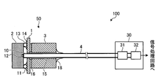
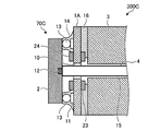
- FIG. 1 is a cross-sectional view of an optical element module 50 according to Embodiment 1 of the present invention.
- FIG. 2 is a cross-sectional view of a light transmission module 100 using the light element module 50 of FIG.
- FIG. 3 is a cross-sectional view of a fixed portion of the optical element module 50 and the optical fiber 4 of the light transmission module 100 of FIG.
- FIG. 4 is a plan view of the hole 10 of the substrate 1 of the light transmission module 100 of FIG. 2 as viewed from the surface emitting laser 2 side.
- the optical transmission module 100 transmits an optical signal to the optical element module 50, the optical fiber 4 for transmitting an optical signal, and the optical element module 50, or transmits an optical signal from the optical element module 50.
- an optical element module 30 for receiving.
- the light element module 50 and the light element module 30 function as a transmission module or a reception module, but when one functions as a transmission module, the other functions as a reception module.
- the case where the light element module 50 is a transmission module and the light element module 30 is a reception module will be described.
- the optical element module 50 includes a substrate 1, a surface emitting laser 2 as a light emitting element mounted on the substrate 1, and a guide holding member 3 mounted on the surface of the substrate 1 facing the mounting surface of the surface emitting laser 2. Equipped with The optical fiber 4 is bonded to the optical element module 50, and the optical element module 30 is connected to the other end face of the optical fiber 4.
- the light element module 30 receives the light signal output from the surface emitting laser 2 and converts the impedance of the converted current signal into a voltage signal by converting the current signal into a light receiving element 31 that is a photodiode (hereinafter referred to as PD) that performs light-current conversion.
- a transimpedance amplifier 32 hereinafter referred to as TIA 32.
- the light element module 30 is further connected to an external signal processing circuit via the TIA 32.
- the guide holding member 3 and the surface emitting laser 2 are arranged and mounted in the thickness direction of the substrate 1 on the facing surface of the substrate 1.
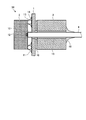
- the substrate 1 an FPC substrate, a ceramic substrate, a glass-epoxy substrate, a glass substrate, a Si substrate or the like is used.
- a connection electrode 11 is formed on the substrate 1, and an electrical signal is transmitted to the surface emitting laser 2 through the connection electrode 11.
- the surface emitting laser 2 is a flip chip type mounted on the substrate 1 such that the light emitting unit 12 faces the substrate 1.
- an Au bump 13 is formed on the surface emitting laser 2 and is bonded onto the connection electrode 11 of the substrate 1 by ultrasonic waves.
- An adhesive 14 such as an underfill material or a side fill material is injected into the joint portion, and the adhesive 14 is cured and mounted.
- solder paste or the like may be printed on the substrate 1 without using the Au bumps 13 and the surface emitting laser 2 may be disposed, and then the solder may be melted and mounted by reflow or the like.
- solder bumps may be formed on the surface-emitting laser 2 and mounted and solder-melted on the connection electrodes 11 of the substrate 1 using a mounting apparatus.
- the guide holding member 3 has a cylindrical through hole 15 having substantially the same diameter as the outer diameter of the optical fiber 4 to be held.
- the through hole 15 may have a prismatic shape as long as the inner surface can hold the optical fiber 4 in addition to a cylindrical shape.
- the material of the guide holding member 3 is ceramic, Si, glass, a metal member such as SUS, or the like.
- the substrate 1 has a hole 10 for transmitting and receiving an optical signal to and from the surface emitting laser 2.
- the inner diameter of the hole 10 is equal to or slightly larger than the inner diameter of the through hole 15.
- the optical fiber 4 inserted into the through hole 15 of the guide holding member 3 and mounted on the optical element module 50 receives the light emitted from the light emitting unit 12 of the surface emitting laser 2 through the hole 10.
- the center of the light emitting portion 12 of the surface emitting laser 2 and the center of the hole 10 are aligned using a two-field optical system, and the hole 10 directly below the light emitting portion 12. Implement to be located.
- the center of the light emitting portion 12 of the surface emitting laser 2 and the center of the through hole 15 are aligned and mounted using a two-field optical system.
- the mounting of the optical fiber 4 on the optical element module 50 is performed through the through hole 15.
- the optical element module 50 can adjust the distance from the end surface of the inserted optical fiber 4 to the light emitting unit 12 between the end surface of the through hole 15 on the surface emitting laser 2 side and the light emitting unit 12. And 17.
- a space 17 is a gap between the surface emitting laser 2 and the substrate 1.
- the optical fiber 4 is inserted into the through hole 15, is inserted through the hole 10 to the vicinity of the light emitting unit 12, and can efficiently input the light output from the light emitting unit 12 with the guide holding member 3 with the adhesive 18. It joins and it becomes the light transmission module 100.
- FIG. When the optical fiber 4 is simply joined, the light emitting portion 12 and the end face of the optical fiber 4 may be brought into contact and joined.
- the optical fiber 4 comprises a core 19 for transmitting light and a cladding 20 provided on the outer periphery of the core 19 and is inserted into the through hole 15 in a state not covered by a jacket of resin or the like.
- the outer diameter of the optical fiber 4 is the diameter of the cladding 20.
- the diameter of the core 19 is about 50 ⁇ m
- the light emitting region of the light emitting unit 12 of the surface emitting laser 2 is a circle of about 20 ⁇ m.
- the light emitting area of the light emitting unit 12 is included in FIG.
- the surface emitting laser 2 receives an electrical signal from an electronic device (not shown) mounted on the substrate 1, converts the received electrical signal into an optical signal, and emits the light. 12 is turned on / off, an optical signal output from the light emitting unit 12 is input to the optical fiber 4, the optical fiber 4 transmits the optical signal to a signal processing device (not shown), etc., and data is transmitted.
- the optical transmission module 100 can easily position the optical fiber 4 with only the guide holding member 3 and can also hold the optical fiber 4, so that downsizing can be achieved. In addition, optical coupling between the optical fiber 4 and the surface emitting laser 2 becomes possible without deteriorating the bonding strength of the optical fiber 4.
- the light transmission module 100 performing optical communication between the surface emitting laser 2 and the optical fiber 4 has been described, but a light transmission module in which the surface emitting laser 2 is changed to a light receiving element as an optical element. Also in this case, the optical fiber 4 can be easily positioned and held only by the guide holding member 3. Therefore, the optical transmission module having the surface emitting laser 2 mounted thereon can be miniaturized as well as the optical fiber 4 and the light receiving element can be optically coupled without deteriorating the bonding strength of the optical fiber 4.
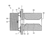
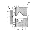
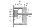
- FIG. 5 is a cross-sectional view of the optical element module 60 according to the second embodiment.
- FIG. 6 is a perspective view of a guide holding member 3A used in the second embodiment.
- FIG. 7 is a cross-sectional view of the light transmission module 200 in which the optical fiber 4 is inserted and fixed to the optical element module 60 of FIG. Although the light transmission module 200 of FIG. 7 is formed of the optical element module 60 and the optical fiber 4, the light element is not provided on the other end face of the optical fiber 4 as in the light transmission module 100 of the first embodiment.
- the module 30 may be connected.
- tapers 21 and 22 are formed at both ends of the through hole 15 respectively.
- the guide holding member 3A is mounted on the substrate 1 by applying the adhesive 16 to the mounting surface of the substrate 1 and then mounting the guide holding member 3A on the adhesive 16 by an apparatus such as a bonder.
- the agent 16 is cured and mounted.
- the adhesive 16 is formed in the hole 10 of the substrate 1 And may be cured. If the adhesive 16 protrudes into the hole 10 and is hardened, there arises a problem that the optical fiber 4 can not be inserted into the hole 10.
- the excess adhesive 16 remains in the taper 21 even if the supply amount of the adhesive 16 is excessive, and the hole 10 is formed. There is no protrusion inside and the insertion of the optical fiber 4 can be performed without any problem. Thereby, the yield at the time of optical element module 60 manufacture can be improved.
- the optical fiber 4 is inserted into the through hole 15 in which the taper 22 is formed on the insertion side, is inserted through the hole 10 to the vicinity of the light emitting unit 12, and is output from the light emitting unit 12. It is joined with the guide holding member 3A by the adhesive 18 at a position where light can be efficiently input.
- the optical fiber 4 can be easily inserted into the through hole 15. Further, since the adhesive 18 is supplied into the taper 22 to bond the optical fiber 4 and the guide holding member 3A, the bonding area between the guide holding member 3A and the optical fiber 4 can be increased, and the bonding strength can be improved. it can.
- a cylindrical groove having a diameter larger than the inner diameter of the through hole 15 may be formed at both end portions of the through hole 15.
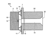
- an optical device module 60B shown in FIG. 8 is exemplified.
- the taper 21 is formed only on the side in contact with the substrate 1 in the through hole 15 of the guide holding member 3B.
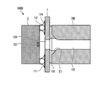
- an optical device module 60C shown in FIG. 9 is exemplified.
- the through hole 15 of the guide holding member 3C is formed with a taper 22 only on the optical fiber 4 insertion opening side.
- the adhesive 18 is used.
- the adhesion area can be increased and the adhesion strength can be improved by supplying.
- the through hole 15 may have an integral tapered shape from the side of the insertion opening of the optical fiber 4 to the side of the outlet.
- a holding portion having substantially the same diameter as the outer diameter of the optical fiber 4 is provided on the outlet side of the optical fiber 4 to prevent misalignment when bonding the optical fiber 4 to the guide holding member 3C. It is preferable to be able to align.
- FIG. 10 is a cross-sectional view of the light transmission module 300 according to the third embodiment.
- FIG. 11 is a plan view of the hole 10 of the substrate 1A of the light transmission module 300 of FIG. 10 as viewed from the surface emitting laser 2 side.
- the light transmission module 300 of FIG. 10 is formed of the optical element module 70 and the optical fiber 4, the light element is not provided on the other end face of the optical fiber 4 as in the light transmission module 100 of the first embodiment.
- the module 30 may be connected.
- the convex member 23 and the convex member 24 are formed around the hole 10 of the substrate 1A.
- the convex member 23 has a short cylindrical shape formed around the hole 10 on the mounting side of the guide holding member 3A of the substrate 1A.
- the convex member 24 has a short cylindrical shape formed around the hole 10 on the mounting side of the surface emitting laser 2 of the substrate 1A.
- the inner diameters of the convex member 23 and the convex member 24 are the same as or slightly larger than the diameter of the hole 10.
- FIG. 11 is a plan view of the hole 10 of the substrate 1A of the light transmission module 300 of FIG.
- the convex member 23 has the same shape as the convex member 24 and
- the plan view of the hole portion 10 of the substrate 1A of the light transmission module 300 viewed from the guide member 3A side is the same as FIG. 11 (the convex member 24 becomes the convex member 23).
- the convex member 23 and the convex member 24 are formed of a resist or the like, and the resist is applied to the surface of the substrate 1A, and formed into a desired shape by a photolithography process.
- the guide holding member 3A is mounted on the substrate 1A by applying the adhesive 16 to the outer peripheral portion of the convex member 23, which is the mounting surface of the substrate 1A, and then using the guide holding member 3A with an apparatus such as a bonder. It mounts on the board
- the adhesive 16 is blocked by the convex member 23 even when a large amount of the adhesive 16 is applied.
- the adhesive 16 flows into the taper 21 of the guide holding member 3A, the adhesive 16 can be prevented from sticking out into the hole 10, so that the optical fiber 4 can be inserted without any problem. Thereby, the yield at the time of light transmission module 300 manufacture can be improved.
- the surface emitting laser 2 is mounted on the substrate 1A by forming an Au bump 13 on the connection surface of the surface emitting laser 2 with the substrate 1A and arranging the Au bump 13 on the connection electrode 11 of the substrate 1A. Bonding is performed by an ultrasonic device, the adhesive 14 is injected into the joint, and the adhesive 14 is cured and mounted.
- the convex member 24 clamps the adhesive 14 by forming the convex member 24 around the hole 10 on the mounting side of the surface emitting laser 2 of the substrate 1A. Thereby, the protrusion of the adhesive 14 into the hole 10 can be prevented, and the yield at the time of manufacturing the light transmission module 300 can be improved because the insertion of the optical fiber 4 can be performed without any problem.
- a light transmission module 300B shown in FIG. 12 is exemplified.
- the convex member 24 is formed only around the hole 10 of the surface emitting laser 2 mounting surface of the substrate 1B.
- the convex member 24 is formed around the hole 10 of the surface-emitting laser 2 mounting surface to prevent the adhesive 14 from protruding into the hole 10, and the insertion of the optical fiber 4 is a problem. It can be done without. Further, since the taper 21 is formed in the through hole 15 of the guide holding member 3B on the side in contact with the substrate 1B, the adhesive 16 can be prevented from protruding into the hole 10.
- a light transmission module 300C shown in FIG. 13 is exemplified.
- the convex members 23 and 24 are formed around the hole 10 of the substrate 1A. Further, in the second modification, no taper is formed in the through hole 15 on the substrate 1A side of the guide holding member 3.
- the convex member 24 is formed on the periphery of the hole 10 of the surface emitting laser 2 mounting surface to prevent the adhesive 14 from protruding into the hole 10, thereby causing the optical fiber 4 to be inserted. It can be done without.
- the convex member 23 Furthermore, by forming the convex member 23 around the hole 10 of the mounting surface of the guide holding member 3, the protrusion of the adhesive 16 into the hole 10 is prevented, and the optical fiber 4 is inserted without problems. Can. Even if the convex member 23 is formed around the through hole 15 of the guide holding member 3, the same effect can be obtained.
- a light transmission module 300D shown in FIG. 14 is exemplified.
- the convex member 23 is formed only around the hole 10 on the surface on which the guide holding member 3 is mounted on the substrate 1D.
- the convex member 23 is formed around the hole 10 of the mounting surface of the guide holding member 3 to prevent the adhesive 16 from protruding into the hole 10, and the insertion of the optical fiber 4 is a problem. It can be done without.
- the convex member 23 is formed around the through hole 15 of the guide holding member 3, the same effect can be obtained.
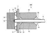
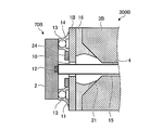
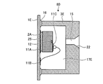
- Embodiment 4 The light transmission module 400 according to the fourth embodiment uses, as an optical element, a wire bonding type surface emitting laser mounted on a substrate such that the light emitting unit is positioned opposite to the mounting surface with the substrate.
- FIG. 15 is a cross-sectional view of the optical element module 80 according to the fourth embodiment.
- FIG. 16 is a cross-sectional view of the light transmission module 400 in which the optical fiber 4 is inserted and fixed to the optical element module 80 of FIG.
- the light transmission module 400 of FIG. 16 is formed of the optical element module 80 and the optical fiber 4, the optical element is provided on the other end face of the optical fiber 4 as in the light transmission module 100 of the first embodiment.
- the module 30 may be connected.
- connection electrode 11A and the connection electrode 11B are formed on the substrate 1E.
- a conductive adhesive 25 such as Ag paste or solder paste is applied on the connection electrode 11A, and the surface emitting laser 2A is disposed so that the light emitting unit 12 is located opposite to the mounting surface with the substrate 1E.
- the agent 25 is heated to die-bond the surface emitting laser 2A to the connection electrode 11A.
- a connection electrode 11C is formed on the light emitting portion 12 side of the surface emitting laser 2A, and the connection electrode 11C and the connection electrode 11B are wire-bonded by an Au wire or the like.
- the wire bonding portion may be reinforced by a resin adhesive as required.
- the guide holding member 3E has a space 17E for housing the surface emitting laser 2A inside, and is mounted on the surface emitting laser 2A mounting surface of the substrate 1E. After applying the adhesive 16 to the substrate 1E, the guide holding member 3E is mounted on the adhesive 16 by a bonder or the like, and the adhesive 16 is cured to mount the guide holding member 3E. In mounting the guide holding member 3E on the substrate 1E, the center of the light emitting portion 12 of the surface emitting laser 2 and the center of the through hole 15 are aligned and mounted using a two-field optical system.
- the mounting of the optical fiber 4 on the optical element module 80 is performed through the through hole 15.
- the through hole 15 has a cylindrical shape having a diameter substantially the same as the outer diameter of the optical fiber 4.
- a taper 22 is formed on the optical fiber 4 insertion side of the through hole 15.
- the optical fiber 4 is inserted into the through hole 15 through the taper 22 and is inserted to the vicinity of the light emitting unit 12 and can efficiently input the light output from the light emitting unit 12 with the guide holding member 3E with the adhesive 18 It is joined.
- the light transmission module 400 according to the fourth embodiment is obtained.
- the taper 22 is formed on the through hole 15 on the side where the optical fiber 4 is inserted, so that the optical fiber 4 can be easily inserted into the through hole 15. Furthermore, since the adhesive 18 is supplied into the taper 22 to bond the optical fiber 4 and the guide holding member 3E, the bonding area between the guide holding member 3E and the optical fiber 4 can be increased, and the bonding strength can be improved. it can.
- the surface emitting laser 2A and the guide holding member 3E are collectively mounted on one side surface of the substrate 1E. This enables the manufacture of the optical transmission module 400 with a high degree of freedom in design.
- the manufacturing method of the light element module, the light transmission module, and the light transmission module according to the present invention is suitable for use in high-speed signal transmission between an imaging element having a large number of pixels and a signal processing apparatus. Further, the light transmission module according to the present invention is particularly suitable for applications where data communication is performed at high speed and miniaturization is required, such as, for example, an endoscope and an ultrasound imaging system (ultrasound endoscope).
Abstract
La présente invention concerne un module à éléments optiques, un module DE transmission optique et un procédé de fabrication dudit module de transmission optique par lequel il est possible d'émettre un signal haute vitesse entre un élément de capture à grande quantité de pixels et un dispositif de traitement de signaux, et avec lequel une miniaturisation est possible. Le module à éléments optiques (50) comprend un laser d'émission de lumière planaire (2) qui réalise une sortie d'un signal optique, un substrat (1) sur lequel ledit laser (2) est monté, et un élément de retenue de guidage (3) comprenant en outre un trou traversant (15) permettant de faire passer une fibre optique qui reçoit une entrée du signal optique qui est sorti dudit laser (2) et qui est monté en position alignée sur ledit laser (2) dans le sens de l'épaisseur du substrat (1). Le trou traversant (15) possède une forme de colonne présentant approximativement le même diamètre que le diamètre externe de la fibre optique.
Priority Applications (2)
| Application Number | Priority Date | Filing Date | Title |
|---|---|---|---|
| EP12814657.8A EP2735899B1 (fr) | 2011-07-21 | 2012-07-17 | Module à éléments optiques, module de transmission optique et procédé de fabrication d'un module de transmission optique |
| US14/104,345 US9385249B2 (en) | 2011-07-21 | 2013-12-12 | Optical element module, optical transmission module, and method of manufacturing optical transmission module |
Applications Claiming Priority (2)
| Application Number | Priority Date | Filing Date | Title |
|---|---|---|---|
| JP2011-159847 | 2011-07-21 | ||
| JP2011159847A JP5809866B2 (ja) | 2011-07-21 | 2011-07-21 | 光素子モジュール、光伝送モジュール、および光伝送モジュールの製造方法 |
Related Child Applications (1)
| Application Number | Title | Priority Date | Filing Date |
|---|---|---|---|
| US14/104,345 Continuation US9385249B2 (en) | 2011-07-21 | 2013-12-12 | Optical element module, optical transmission module, and method of manufacturing optical transmission module |
Publications (1)
| Publication Number | Publication Date |
|---|---|
| WO2013011983A1 true WO2013011983A1 (fr) | 2013-01-24 |
Family
ID=47558160
Family Applications (1)
| Application Number | Title | Priority Date | Filing Date |
|---|---|---|---|
| PCT/JP2012/068108 WO2013011983A1 (fr) | 2011-07-21 | 2012-07-17 | Module à éléments optiques, module de transmission optique et procédé de fabrication d'un module de transmission optique |
Country Status (4)
| Country | Link |
|---|---|
| US (1) | US9385249B2 (fr) |
| EP (1) | EP2735899B1 (fr) |
| JP (1) | JP5809866B2 (fr) |
| WO (1) | WO2013011983A1 (fr) |
Cited By (4)
| Publication number | Priority date | Publication date | Assignee | Title |
|---|---|---|---|---|
| WO2013129026A1 (fr) * | 2012-02-28 | 2013-09-06 | オリンパス株式会社 | Module de conversion photoélectrique et unité de transmission optique |
| EP3072434A4 (fr) * | 2013-11-18 | 2017-07-19 | Olympus Corporation | Endoscope |
| EP3075298A4 (fr) * | 2013-11-28 | 2017-07-26 | Olympus Corporation | Endoscope |
| US11762156B2 (en) | 2018-04-26 | 2023-09-19 | Olympus Corporation | Optical module for endoscope, endoscope, and manufacturing method of optical module for endoscope |
Families Citing this family (23)
| Publication number | Priority date | Publication date | Assignee | Title |
|---|---|---|---|---|
| JP6411088B2 (ja) | 2013-09-26 | 2018-10-24 | オリンパス株式会社 | 光伝送モジュールおよび内視鏡 |
| JP6321933B2 (ja) * | 2013-09-26 | 2018-05-09 | オリンパス株式会社 | 光伝送モジュール、及び内視鏡 |
| JP6226782B2 (ja) | 2014-03-13 | 2017-11-08 | オリンパス株式会社 | 光伝送モジュールおよび光伝送モジュールの製造方法 |
| JP6382586B2 (ja) * | 2014-06-11 | 2018-08-29 | オリンパス株式会社 | 光伝送モジュール、および光伝送モジュールの製造方法 |
| JP6382585B2 (ja) * | 2014-06-11 | 2018-08-29 | オリンパス株式会社 | 光伝送モジュール |
| JP2016004130A (ja) * | 2014-06-16 | 2016-01-12 | オリンパス株式会社 | 光伝送モジュールおよび光伝送モジュールの製造方法 |
| JP6485840B2 (ja) * | 2015-01-23 | 2019-03-20 | オリンパス株式会社 | 光伝送モジュールおよび内視鏡 |
| US9541717B2 (en) | 2015-01-30 | 2017-01-10 | Avago Technologies General IP (Singapore) Pta. Ltd. | Optoelectronic assembly incorporating an optical fiber alignment structure |
| JPWO2016185537A1 (ja) * | 2015-05-18 | 2018-03-01 | オリンパス株式会社 | 内視鏡、および光伝送モジュール |
| JPWO2016189691A1 (ja) * | 2015-05-27 | 2018-03-15 | オリンパス株式会社 | 内視鏡および光伝送モジュール |
| JPWO2017109930A1 (ja) * | 2015-12-25 | 2018-10-18 | オリンパス株式会社 | 撮像モジュールおよび内視鏡 |
| US10186584B2 (en) | 2016-08-18 | 2019-01-22 | Uchicago Argonne, Llc | Systems and methods for forming diamond heterojunction junction devices |
| WO2018134933A1 (fr) * | 2017-01-19 | 2018-07-26 | オリンパス株式会社 | Module de optique et endoscope |
| WO2018138778A1 (fr) | 2017-01-24 | 2018-08-02 | オリンパス株式会社 | Endoscope |
| US20190129108A1 (en) | 2017-10-31 | 2019-05-02 | Versalume LLC | Modular Laser Connector Packaging System and Method |
| WO2019163014A1 (fr) * | 2018-02-21 | 2019-08-29 | オリンパス株式会社 | Module optique d'endoscope, endoscope et méthode de fabrication d'un module optique d'endoscope |
| WO2020075253A1 (fr) | 2018-10-11 | 2020-04-16 | オリンパス株式会社 | Dispositif d'imagerie endoscopique, endoscope et procédé de fabrication de dispositif d'imagerie endoscopique |
| US10551542B1 (en) | 2018-12-11 | 2020-02-04 | Corning Incorporated | Light modules and devices incorporating light modules |
| WO2020217277A1 (fr) * | 2019-04-22 | 2020-10-29 | オリンパス株式会社 | Procédé de fabrication d'un dispositif d'imagerie destiné à un endoscope, dispositif d'imagerie destiné à un endoscope, et endoscope |
| CN110412700B (zh) * | 2019-07-26 | 2022-05-17 | 西安微电子技术研究所 | 一种综合电子高速光互连模块集成结构及集成方法 |
| JP7399180B2 (ja) * | 2019-09-30 | 2023-12-15 | 京セラ株式会社 | 光素子搭載用パッケージ、電子装置及び電子モジュール |
| WO2021260854A1 (fr) * | 2020-06-24 | 2021-12-30 | オリンパス株式会社 | Module optique pour endoscope et endoscope |
| US20220196875A1 (en) * | 2020-12-23 | 2022-06-23 | TE Connectivity Services Gmbh | Light source for an optical sensor |
Citations (9)
| Publication number | Priority date | Publication date | Assignee | Title |
|---|---|---|---|---|
| JPS594509U (ja) * | 1982-06-29 | 1984-01-12 | 日本板硝子株式会社 | 光ファイバー端子 |
| JPS63107408U (fr) * | 1986-12-26 | 1988-07-11 | ||
| JPH0990175A (ja) | 1995-09-28 | 1997-04-04 | Kyocera Corp | 光通信用モジュール |
| JP2005286284A (ja) * | 2004-02-03 | 2005-10-13 | Sony Chem Corp | 機能素子実装モジュール並びに光機能素子実装モジュール及びその製造方法 |
| JP2006145787A (ja) * | 2004-11-18 | 2006-06-08 | Hakusan Mfg Co Ltd | 光コネクタおよびその製造方法 |
| JP2007316548A (ja) * | 2006-05-29 | 2007-12-06 | Fujikura Ltd | 光ファイバアレイ |
| JP2009047937A (ja) * | 2007-08-20 | 2009-03-05 | Sony Corp | 光送信/光受信モジュール及び光モジュールの製造方法並びに光通信モジュール |
| JP2009206158A (ja) * | 2008-02-26 | 2009-09-10 | Sumitomo Electric Ind Ltd | レーザモジュールおよびレーザ装置 |
| JP2010048940A (ja) * | 2008-08-20 | 2010-03-04 | Fuji Xerox Co Ltd | 光学装置 |
Family Cites Families (11)
| Publication number | Priority date | Publication date | Assignee | Title |
|---|---|---|---|---|
| US6243508B1 (en) * | 1999-06-01 | 2001-06-05 | Picolight Incorporated | Electro-opto-mechanical assembly for coupling a light source or receiver to an optical waveguide |
| JP2002252430A (ja) * | 2001-02-26 | 2002-09-06 | Ricoh Co Ltd | 光通信システム |
| JP2002250846A (ja) * | 2001-02-26 | 2002-09-06 | Seiko Epson Corp | 光モジュール及びその製造方法並びに光伝達装置 |
| JP2002311305A (ja) * | 2001-04-13 | 2002-10-23 | Seiko Epson Corp | 光ファイバ支持部材およびこれを用いた光送信装置 |
| WO2004097486A1 (fr) * | 2003-04-29 | 2004-11-11 | Pirelli & C. S.P.A. | Structure de couplage pour fibres optiques et procede d'elaboration |
| JP3991318B2 (ja) * | 2004-01-20 | 2007-10-17 | セイコーエプソン株式会社 | 光モジュールの製造方法、光通信装置、電子機器 |
| EP1741136A2 (fr) * | 2004-04-13 | 2007-01-10 | SA Intexys | Procede de fabrication de circuits electroniques et optoelectroniques |
| US7352935B2 (en) * | 2004-08-17 | 2008-04-01 | Kabushiki Kaisha Toshiba | Optoelectronic conversion header, LSI package with interface module, method of manufacturing optoelectronic conversion header, and optical interconnection system |
| JP4829902B2 (ja) * | 2006-01-31 | 2011-12-07 | 富士通株式会社 | 光モジュールおよびその製造方法 |
| JP5049145B2 (ja) * | 2008-01-22 | 2012-10-17 | 日東電工株式会社 | 光導波路デバイスの製法 |
| US9442255B2 (en) * | 2010-06-29 | 2016-09-13 | Ultra Communications, Inc. | Low profile fiber-to-module interface with relaxed alignment tolerances |
-
2011
- 2011-07-21 JP JP2011159847A patent/JP5809866B2/ja active Active
-
2012
- 2012-07-17 EP EP12814657.8A patent/EP2735899B1/fr not_active Not-in-force
- 2012-07-17 WO PCT/JP2012/068108 patent/WO2013011983A1/fr active Application Filing
-
2013
- 2013-12-12 US US14/104,345 patent/US9385249B2/en active Active
Patent Citations (9)
| Publication number | Priority date | Publication date | Assignee | Title |
|---|---|---|---|---|
| JPS594509U (ja) * | 1982-06-29 | 1984-01-12 | 日本板硝子株式会社 | 光ファイバー端子 |
| JPS63107408U (fr) * | 1986-12-26 | 1988-07-11 | ||
| JPH0990175A (ja) | 1995-09-28 | 1997-04-04 | Kyocera Corp | 光通信用モジュール |
| JP2005286284A (ja) * | 2004-02-03 | 2005-10-13 | Sony Chem Corp | 機能素子実装モジュール並びに光機能素子実装モジュール及びその製造方法 |
| JP2006145787A (ja) * | 2004-11-18 | 2006-06-08 | Hakusan Mfg Co Ltd | 光コネクタおよびその製造方法 |
| JP2007316548A (ja) * | 2006-05-29 | 2007-12-06 | Fujikura Ltd | 光ファイバアレイ |
| JP2009047937A (ja) * | 2007-08-20 | 2009-03-05 | Sony Corp | 光送信/光受信モジュール及び光モジュールの製造方法並びに光通信モジュール |
| JP2009206158A (ja) * | 2008-02-26 | 2009-09-10 | Sumitomo Electric Ind Ltd | レーザモジュールおよびレーザ装置 |
| JP2010048940A (ja) * | 2008-08-20 | 2010-03-04 | Fuji Xerox Co Ltd | 光学装置 |
Cited By (7)
| Publication number | Priority date | Publication date | Assignee | Title |
|---|---|---|---|---|
| WO2013129026A1 (fr) * | 2012-02-28 | 2013-09-06 | オリンパス株式会社 | Module de conversion photoélectrique et unité de transmission optique |
| US9625664B2 (en) | 2012-02-28 | 2017-04-18 | Olympus Corporation | Photoelectric conversion module and optical transmission unit |
| EP3072434A4 (fr) * | 2013-11-18 | 2017-07-19 | Olympus Corporation | Endoscope |
| US10088669B2 (en) | 2013-11-18 | 2018-10-02 | Olympus Corporation | Endoscope |
| EP3075298A4 (fr) * | 2013-11-28 | 2017-07-26 | Olympus Corporation | Endoscope |
| US10568491B2 (en) | 2013-11-28 | 2020-02-25 | Olympus Corporation | Endoscope |
| US11762156B2 (en) | 2018-04-26 | 2023-09-19 | Olympus Corporation | Optical module for endoscope, endoscope, and manufacturing method of optical module for endoscope |
Also Published As
| Publication number | Publication date |
|---|---|
| US20140097459A1 (en) | 2014-04-10 |
| EP2735899A1 (fr) | 2014-05-28 |
| JP5809866B2 (ja) | 2015-11-11 |
| US9385249B2 (en) | 2016-07-05 |
| EP2735899B1 (fr) | 2018-09-05 |
| EP2735899A4 (fr) | 2015-03-25 |
| JP2013025092A (ja) | 2013-02-04 |
Similar Documents
| Publication | Publication Date | Title |
|---|---|---|
| WO2013011983A1 (fr) | Module à éléments optiques, module de transmission optique et procédé de fabrication d'un module de transmission optique | |
| US9762329B2 (en) | Optical transmission module and imaging device | |
| JP6321933B2 (ja) | 光伝送モジュール、及び内視鏡 | |
| US9207412B2 (en) | Optical transmission module and endoscope | |
| US9435925B2 (en) | Optical fiber cable connecting structure | |
| US10088669B2 (en) | Endoscope | |
| WO2018173261A1 (fr) | Endoscope et module composite photoélectrique | |
| WO2018150512A1 (fr) | Module optique, endoscope et procédé de fabrication de module optique | |
| JP2009169116A (ja) | 光モジュールおよびその作製方法 | |
| US20180078114A1 (en) | Endoscope and optical transmission module | |
| JP2009047937A (ja) | 光送信/光受信モジュール及び光モジュールの製造方法並びに光通信モジュール | |
| US20170315310A1 (en) | Optical transmission module and endoscope | |
| US11762156B2 (en) | Optical module for endoscope, endoscope, and manufacturing method of optical module for endoscope | |
| US20180368659A1 (en) | Optical transmitter and endoscope | |
| JP2015097588A (ja) | 光伝送モジュール及び内視鏡 | |
| JP6081160B2 (ja) | 光素子モジュール、光伝送モジュール、および光伝送モジュールの製造方法 | |
| WO2017141369A1 (fr) | Module de transmission optique, et endoscope | |
| US10838194B2 (en) | Optical transmission module and endoscope | |
| JP2016001237A (ja) | 光伝送モジュール | |
| WO2020217277A1 (fr) | Procédé de fabrication d'un dispositif d'imagerie destiné à un endoscope, dispositif d'imagerie destiné à un endoscope, et endoscope | |
| JP2004336025A (ja) | 光モジュール、光モジュール実装基板、光伝送モジュール、双方向光伝送モジュール、光モジュールの製造方法 | |
| JP2018105907A (ja) | 光モジュールおよび内視鏡 |
Legal Events
| Date | Code | Title | Description |
|---|---|---|---|
| 121 | Ep: the epo has been informed by wipo that ep was designated in this application |
Ref document number: 12814657 Country of ref document: EP Kind code of ref document: A1 |
|
| WWE | Wipo information: entry into national phase |
Ref document number: 2012814657 Country of ref document: EP |
|
| NENP | Non-entry into the national phase |
Ref country code: DE |