WO2012176914A1 - 基板処理時間設定方法及び記憶媒体 - Google Patents
基板処理時間設定方法及び記憶媒体 Download PDFInfo
- Publication number
- WO2012176914A1 WO2012176914A1 PCT/JP2012/066090 JP2012066090W WO2012176914A1 WO 2012176914 A1 WO2012176914 A1 WO 2012176914A1 JP 2012066090 W JP2012066090 W JP 2012066090W WO 2012176914 A1 WO2012176914 A1 WO 2012176914A1
- Authority
- WO
- WIPO (PCT)
- Prior art keywords
- time
- lot
- substrate processing
- standby time
- substrate
- Prior art date
- Legal status (The legal status is an assumption and is not a legal conclusion. Google has not performed a legal analysis and makes no representation as to the accuracy of the status listed.)
- Ceased
Links
Images



Classifications
-
- H—ELECTRICITY
- H10—SEMICONDUCTOR DEVICES; ELECTRIC SOLID-STATE DEVICES NOT OTHERWISE PROVIDED FOR
- H10P—GENERIC PROCESSES OR APPARATUS FOR THE MANUFACTURE OR TREATMENT OF DEVICES COVERED BY CLASS H10
- H10P72/00—Handling or holding of wafers, substrates or devices during manufacture or treatment thereof
- H10P72/06—Apparatus for monitoring, sorting, marking, testing or measuring
- H10P72/0612—Production flow monitoring, e.g. for increasing throughput
-
- G—PHYSICS
- G05—CONTROLLING; REGULATING
- G05B—CONTROL OR REGULATING SYSTEMS IN GENERAL; FUNCTIONAL ELEMENTS OF SUCH SYSTEMS; MONITORING OR TESTING ARRANGEMENTS FOR SUCH SYSTEMS OR ELEMENTS
- G05B19/00—Program-control systems
- G05B19/02—Program-control systems electric
- G05B19/418—Total factory control, i.e. centrally controlling a plurality of machines, e.g. direct or distributed numerical control [DNC], flexible manufacturing systems [FMS], integrated manufacturing systems [IMS] or computer integrated manufacturing [CIM]
- G05B19/41865—Total factory control, i.e. centrally controlling a plurality of machines, e.g. direct or distributed numerical control [DNC], flexible manufacturing systems [FMS], integrated manufacturing systems [IMS] or computer integrated manufacturing [CIM] characterised by job scheduling, process planning, material flow
-
- G—PHYSICS
- G05—CONTROLLING; REGULATING
- G05B—CONTROL OR REGULATING SYSTEMS IN GENERAL; FUNCTIONAL ELEMENTS OF SUCH SYSTEMS; MONITORING OR TESTING ARRANGEMENTS FOR SUCH SYSTEMS OR ELEMENTS
- G05B2219/00—Program-control systems
- G05B2219/30—Nc systems
- G05B2219/31—From computer integrated manufacturing till monitoring
- G05B2219/31429—Predict end of job execution, schedule new job beforehand
-
- G—PHYSICS
- G05—CONTROLLING; REGULATING
- G05B—CONTROL OR REGULATING SYSTEMS IN GENERAL; FUNCTIONAL ELEMENTS OF SUCH SYSTEMS; MONITORING OR TESTING ARRANGEMENTS FOR SUCH SYSTEMS OR ELEMENTS
- G05B2219/00—Program-control systems
- G05B2219/30—Nc systems
- G05B2219/45—Nc applications
- G05B2219/45031—Manufacturing semiconductor wafers
-
- Y—GENERAL TAGGING OF NEW TECHNOLOGICAL DEVELOPMENTS; GENERAL TAGGING OF CROSS-SECTIONAL TECHNOLOGIES SPANNING OVER SEVERAL SECTIONS OF THE IPC; TECHNICAL SUBJECTS COVERED BY FORMER USPC CROSS-REFERENCE ART COLLECTIONS [XRACs] AND DIGESTS
- Y02—TECHNOLOGIES OR APPLICATIONS FOR MITIGATION OR ADAPTATION AGAINST CLIMATE CHANGE
- Y02P—CLIMATE CHANGE MITIGATION TECHNOLOGIES IN THE PRODUCTION OR PROCESSING OF GOODS
- Y02P90/00—Enabling technologies with a potential contribution to greenhouse gas [GHG] emissions mitigation
- Y02P90/02—Total factory control, e.g. smart factories, flexible manufacturing systems [FMS] or integrated manufacturing systems [IMS]
Definitions
- the present invention relates to a substrate processing time setting method and a storage medium.
- a substrate processing apparatus that performs plasma processing, for example, dry etching processing or film forming processing, on a semiconductor device wafer (hereinafter simply referred to as “wafer”) as a substrate
- a lot of wafers for example, 25 wafers
- the wafer is taken out from the supplied carrier, and each wafer is subjected to plasma processing in a single wafer.
- the substrate processing apparatus responsible for the latter half of the semiconductor device manufacturing process may be in a standby (idle) state until the end of the plasma processing of all wafers in one lot in the substrate processing apparatus responsible for the first half.
- the idle state plasma processing is not performed in the process module of the substrate processing apparatus, so that the state in the processing chamber of the process module changes from a state optimal for predetermined plasma processing. If the idle state is too long, the state in the processing chamber may change to a state inappropriate for the predetermined plasma processing, so that the carrier of the next lot is supplied and the predetermined plasma processing is performed on each wafer of the carrier. Before, the dummy wafer is carried into the processing chamber, and the dummy wafer is subjected to a dummy processing similar to the predetermined plasma processing, and the state in the processing chamber is changed to a state suitable for the predetermined plasma processing. Further, whether or not to execute the dummy process is determined based on whether or not the time when the idle state is exceeded exceeds a predetermined time (see, for example, Patent Document 1).
- An object of the present invention is to provide a substrate processing time setting method and a storage medium that can eliminate dummy processing as much as possible.
- a substrate processing time setting method in a substrate processing apparatus for performing predetermined processing on a single wafer on one lot of substrates including a plurality of substrates In the substrate processing apparatus, a first supply time for calculating a second lot supplied to the substrate processing apparatus after the supply of the first lot including the substrate that is currently subjected to the predetermined processing is calculated.
- a second calculation step for calculating an expected end time of the predetermined process for all the substrates of the first lot, the calculated expected supply time, and the calculated expected end time
- a determination step for determining whether or not the waiting time is longer than a reference waiting time that requires dummy processing, and when the calculated expected waiting time is equal to or greater than the reference waiting time, the unprocessed in the first lot
- an additional setting step of additionally setting an auxiliary waiting time during the predetermined processing of each of the substrates.
- a substrate processing time setting method is provided.
- the auxiliary waiting time when the auxiliary waiting time is additionally set in the additional setting step, the waiting time continues after the completion of the predetermined processing of all the substrates of the first lot.
- all the auxiliary standby times set are the same length.
- the first calculation step is executed to execute the substrate processing. It is preferable to calculate the expected supply time of the second lot supplied to the apparatus.
- the length of the auxiliary standby time is preferably shorter than the reference standby time.
- a computer storing a program for causing a computer to execute a substrate processing time setting method in a substrate processing apparatus for performing predetermined processing on a single wafer on a lot of substrates including a plurality of substrates.
- the substrate processing time setting method supplies the substrate processing apparatus with the first lot including the substrate that is currently performing the predetermined processing in the substrate processing apparatus.
- the substrate processing time setting method may include the predetermined processing for all the substrates in the first lot when the auxiliary waiting time is additionally set in the additional setting step. Another determination step for determining whether or not another standby time that is a standby time following the end of the process is longer than the reference standby time, and when the other standby time is equal to or greater than the reference standby time, the addition It is preferable to further include a deletion step of deleting the auxiliary waiting time set as described above.
- the expected supply time of the second lot to be supplied to the substrate processing apparatus after the supply of the first lot including the substrate currently undergoing the predetermined processing in the substrate processing apparatus, and the first lot Based on the expected end time of the predetermined processing of all the substrates, an expected standby time that is a standby time after completion of the predetermined processing of all the substrates in the first lot in the substrate processing apparatus is calculated and calculated. If the expected standby time is equal to or greater than the reference standby time that requires dummy processing, the auxiliary standby time is additionally set during the predetermined processing of each unprocessed substrate in the first lot. The end time of the predetermined processing for all the substrates in the lot can be delayed, so that the actual waiting time can be made shorter than the reference waiting time. As a result, dummy processing can be eliminated as much as possible.
- FIG. 1 is a plan view for explaining a substrate processing apparatus and related apparatuses for executing a substrate processing time setting method according to the present embodiment.
- FIG. 1 in a clean room 10 of a semiconductor device manufacturing factory, there are six substrate processing apparatuses 11, a stocker 13 that stocks a large number of carriers 12, and guides 14 that connect the vicinity of each substrate processing apparatus 11 and the stocker 13. And an automatic material handling system (AMHS) 15 such as an OHT (Overhead Hoist Transport).
- AMHS automatic material handling system
- each substrate processing apparatus 11, stocker 13 and AMHS 15 are communicably connected to a host computer (not shown) by wire or wirelessly.
- One carrier 12 accommodates one lot of wafers composed of a plurality of, for example, 25 wafers.
- Each carrier 12 is transported between the stocker 13 and each substrate processing apparatus 11 by the AMHS 15 and, when loaded into each substrate processing apparatus 11, plasma processing is performed on each wafer accommodated in the carrier 12 by the substrate processing apparatus 11, for example, Then, a dry etching process or a film forming process is performed.
- Each substrate processing apparatus 11 takes out a wafer from three load ports 16 that receive the loaded carrier 12, and the carrier 12 received in the load port 16, and accommodates the wafer subjected to plasma processing in the carrier 12.
- a process module 18 for accommodating each wafer in a processing chamber and performing plasma processing on the wafer, and a controller (not shown) for controlling the operation of each module.
- the wafer is transferred from the load port 16 through the loader module 17 and the transfer module 19 to the process chamber of the process module 18 in a single wafer.
- the wafer is transferred from the processing chamber of the process module 18 to the load port 16 via the transfer module 19 and the loader module 17 in a single wafer, and then accommodated in the carrier 12.
- the carrier 12 When each wafer is subjected to plasma processing and one lot of processed wafers are stored in the carrier 12, the carrier 12 is unloaded from the substrate processing apparatus 11, and then the next plasma processing is performed on each wafer by the AMHS 15. It is carried into the substrate processing apparatus 11 to be applied. Therefore, in the same substrate processing apparatus 11, the same plasma processing is repeatedly performed on each wafer of a plurality of lots.
- each process module 18 of the substrate processing apparatus 11 does not perform the plasma processing on the wafer and enters a standby (idle) state.
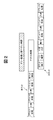
- FIG. 2 is a time chart for explaining idle time.
- the horizontal direction corresponds to the passage of time.
- the carrier 12 containing the wafer of the next lot is carried into the substrate processing apparatus 11 by the AMHS 15 (indicated by “carrying in the next lot C” in the drawing), but each wafer of the next lot is immediately subjected to plasma processing.
- the controller of the substrate processing apparatus 11 informs the host computer of the identification number of the carrier 12 loaded, and inquires about the contents of the plasma processing to be performed on each wafer of the carrier 12 (indicated by “CID confirmation” in the figure). .
- the host computer determines the contents of the plasma processing corresponding to the contacted identification number, contacts the controller of the substrate processing apparatus 11 (indicated by “determined PJ etc.” in the figure), and the contents of the plasma processing, etc.
- the controller that has received the communication controls the operation of each module and first carries the first wafer of the next lot from the carrier 12 into the processing chamber of the process module 18 to perform plasma processing on the wafer.
- the processing and the loading / unloading of wafers between the processing chambers of the carrier 12 through the process module 18 are repeated.
- each process module of the substrate processing apparatus 11 is the time from when the carrier 12 containing the processed wafer of this lot is unloaded until the first wafer of the next lot is subjected to plasma processing.
- the time when 18 does not perform plasma processing on the wafer is defined as “idle time” (standby time).
- the state in the processing chamber changes from the state optimal for the plasma processing.
- the longer the idle time the more the state in the processing chamber becomes inappropriate for the plasma processing. Approaching. Therefore, when the idle time is longer than the time (hereinafter referred to as “dummy processing required idle time”) (reference standby time) during which the state in the processing chamber changes to a state inappropriate for plasma processing, In order to change the state to a state suitable for plasma processing, dummy processing is performed in the processing chamber of each process module 18.
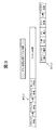
- FIG. 3 is a time chart for explaining the dummy processing.
- the horizontal direction corresponds to the passage of time.
- the idle time is longer than the idle time required for the dummy processing.
- the carrier 12 containing the wafer of the next lot is loaded into the substrate processing apparatus 11, it is immediately subjected to CID confirmation, PJ determination, and the like.
- a dummy wafer that is not used for manufacturing a semiconductor device is carried into the processing chamber of each process module 18 from the outside of the substrate processing apparatus 11 (“Dummy loading” in the figure).
- the dummy process having the content similar to the content of the plasma process received from the host computer is applied to the loaded dummy wafer (indicated by “dummy process” in the figure). Thereby, the state in the processing chamber changes to a state suitable for plasma processing.
- the first wafer of the next lot is carried into the processing chamber of the process module 18 and subjected to plasma processing. Thereafter, the plasma processing of each wafer and the wafer between the carrier 12 and the processing chamber of the process module 18 are performed. Is repeatedly carried in and out.
- the dummy process is an essentially unnecessary process, and there is a possibility that the throughput is lowered and the cost is increased.
- various processing times in the lot are set so as to minimize the idle time that continues after the plasma processing of all the wafers in the lot.
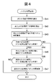
- FIG. 4 is a flowchart showing an idle time addition process as a substrate processing time setting method according to the present embodiment.
- the expected end time of the plasma processing of all wafers in the next lot in the other substrate processing apparatus 11 that performs the plasma processing of the previous process on each wafer before the plasma processing performed on each wafer by the substrate processing apparatus 11. Is calculated by the controller of another substrate processing apparatus 11 and communicated to the host computer.
- the host computer calculates the estimated supply time of the next lot to the substrate processing apparatus 11 based on the predicted completion time in the other substrate processing apparatus 11 (step S41) (first calculation step).
- the calculated expected supply time is notified to the controller of the substrate processing apparatus 11.
- the controller of the substrate processing apparatus 11 calculates the expected end time of plasma processing for all wafers in the lot (step S42) (second calculation step), and further receives the estimated supply time and calculation of the received next lot. Based on the estimated plasma processing end time of the lot, the expected idle time (expected standby time) following the completion of the plasma processing for all the wafers in the lot is calculated (step S43) (third step).
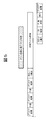
- FIG. 5 is a time chart for explaining the expected idle time.
- the horizontal direction corresponds to the passage of time.
- the carrier 12 containing the processed wafer of this lot is unloaded when it is assumed that dummy processing is not performed regardless of the supply time of the second lot. This corresponds to the time from when the first wafer of the next lot is subjected to plasma processing.
- the controller of the substrate processing apparatus 11 determines whether or not the expected idle time is longer than the idle time required for dummy processing (step S44) (determination step).
- step S44 if the expected idle time is shorter than the idle time required for dummy processing, for example, as shown in FIG. 2, the controller of the substrate processing apparatus 11 sets the plasma processing start time of each unprocessed wafer in this lot, This process is terminated without changing the start time of loading / unloading of each wafer.
- the expected idle time is equal to or longer than the idle time required for dummy processing, as shown in FIG. 6, during the plasma processing of each unprocessed wafer of this lot, more specifically, the plasma of a certain unprocessed wafer.
- the next unprocessed wafer is loaded into the processing chamber of the process module 18 (“loading” in the drawing).
- a supplementary idle time (auxiliary standby time) is additionally set (step S45) (additional setting step).
- the auxiliary idle time is set by the number obtained by subtracting 1 from the number of unprocessed wafers in this lot.
- Each auxiliary idle time has the same length and is set shorter than the idle time required for dummy processing.
- each auxiliary idle time is the time when the carrier 12 containing the plasma-processed wafer of this lot is carried out when the auxiliary idle time is added and set (the right end of “carrying out this lot C” in the figure). Is set so as not to be later than the expected supply time of the next lot (the left end of “next lot C loading” in the figure).
- step S45 the idle time after the plasma processing of all the wafers in this lot when the auxiliary idle time is additionally set in step S45 (hereinafter referred to as “actual idle time”) (other standby time)
- step S46 the controller of the substrate processing apparatus 11 determines whether or not the calculated actual idle time is longer than the dummy processing-required idle time (step S46) (other determination step).
- step S46 if the actual idle time is shorter than the idle time required for the dummy process, this process is terminated. On the other hand, if the actual idle time is equal to or greater than the idle time necessary for the dummy process, it is added in step S45. All the auxiliary idle times set in the above are deleted (step S47) (deletion step), and as shown in FIG. 3, the idle time is returned to a state longer than the dummy process required idle time, and this process is terminated.
- the auxiliary idle time is additionally set during the plasma process for each unprocessed wafer in this lot.
- the plasma processing end time of all the wafers in this lot can be delayed, so that the actual idle time can be made shorter than the dummy processing required idle time.
- dummy processing can be eliminated as much as possible.
- each auxiliary idle time is additionally set in step S45 of FIG. 4, if the actual idle time is equal to or longer than the idle time required for dummy processing, it is necessary to execute dummy processing. That is, dummy processing is further executed after waiting for each auxiliary idle time, and the processing time is unnecessarily extended.
- the actual idle time is equal to or longer than the dummy process-required idle time, all the auxiliary idle times set in step S45 are deleted. As a result, it is possible to prevent further dummy processing from being performed after waiting for each auxiliary idle time, thereby preventing unnecessary increase in processing time.
- each auxiliary idle time set additionally has the same length.
- each auxiliary idle time does not have to be the same length, and each auxiliary idle time is an idle that requires dummy processing. If the actual idle time is shorter than the time required for dummy processing, the length of each auxiliary idle time can be freely set. For example, as shown in FIG. 7, the auxiliary idle time may be set to be shorter as the last wafer of this lot is approached. In this case, since the total amount of idle time immediately before the plasma processing of the first wafer of the next lot can be reduced, the plasma processing can be more stably performed on the first wafer of the next lot.
- the controller of the other substrate processing apparatus 11 makes all of the next lots in the other substrate processing apparatus 11 when the plasma processing (other predetermined processing) of the first wafer of the next lot is completed.
- the estimated end time of the plasma processing of the wafer is calculated and notified to the host computer, and the host computer calculates the estimated supply time of the next lot to the substrate processing apparatus 11 based on the notified estimated end time. Also good. Thereby, it is possible to quickly calculate the expected idle time and determine whether or not the calculated expected idle time is equal to or greater than the dummy process required idle time. As a result, the auxiliary idle time can be additionally set with a time margin.
- the host computer calculates the expected supply time of the next lot to the substrate processing apparatus 11, but the controller of the substrate processing apparatus 11 performs the other substrate processing from the controller of the other substrate processing apparatus 11.
- the expected supply time of plasma processing in the apparatus 11 may be directly received, and the expected supply time may be calculated based on the expected completion time.
- the controller of the substrate processing apparatus 11 calculates the expected idle time, but the host computer receives the expected end time of the plasma processing of all wafers of this lot from the controller of the substrate processing apparatus 11.
- the estimated idle time may be calculated based on the estimated end time and the estimated supply time of the next lot, and the host computer may determine whether the estimated idle time is longer than the idle time required for dummy processing. Good.
- An object of the present invention is to supply a computer or the like a storage medium that records a software program that implements the functions of the above-described embodiments, and the computer CPU reads and executes the program stored in the storage medium. Is also achieved.
- the program itself read from the storage medium realizes the functions of the above-described embodiment, and the program and the storage medium storing the program constitute the present invention.
- Examples of storage media for supplying the program include RAM, NV-RAM, floppy (registered trademark) disk, hard disk, magneto-optical disk, CD-ROM, CD-R, CD-RW, DVD (DVD-). Any optical disc such as ROM, DVD-RAM, DVD-RW, DVD + RW), magnetic tape, non-volatile memory card, other ROM, or the like may be used.
- the program may be supplied to the computer by downloading it from another computer or database (not shown) connected to the Internet, a commercial network, a local area network, or the like.
- the function expansion board or This includes a case where the CPU or the like provided in the function expansion unit performs part or all of the actual processing and the functions of the above-described embodiments are realized by the processing.
- the form of the program may be in the form of object code, a program executed by an interpreter, script data supplied to the OS, and the like.
Landscapes
- Engineering & Computer Science (AREA)
- General Engineering & Computer Science (AREA)
- Manufacturing & Machinery (AREA)
- Quality & Reliability (AREA)
- Physics & Mathematics (AREA)
- General Physics & Mathematics (AREA)
- Automation & Control Theory (AREA)
- Container, Conveyance, Adherence, Positioning, Of Wafer (AREA)
- Drying Of Semiconductors (AREA)
- Chemical Vapour Deposition (AREA)
Abstract
Description
12 キャリア
18 プロセスモジュール
Claims (7)
- 複数枚の基板を含む1ロットの前記基板へ枚葉に所定の処理を施す基板処理装置における基板処理時間設定方法であって、
前記基板処理装置において現在、前記所定の処理を施している前記基板を含む第1のロットの供給後に前記基板処理装置に供給される第2のロットの供給予想時刻を算出する第1の算出ステップと、
前記第1のロットの全ての前記基板の前記所定の処理の終了予想時刻を算出する第2の算出ステップと、
前記算出された供給予想時刻及び前記算出された終了予想時刻に基づいて、前記基板処理装置における前記第1のロットの全ての前記基板の前記所定の処理の終了後に続く待機時間である予想待機時間を算出する第3の算出ステップと、
前記算出された予想待機時間がダミー処理を必要とする基準待機時間よりも長いか否かを判定する判定ステップと、
前記算出された予想待機時間が前記基準待機時間以上である場合、前記第1のロットにおける未処理の各前記基板の前記所定の処理の間に補助待機時間を追加して設定する追加設定ステップとを有することを特徴とする基板処理時間設定方法。 - 前記追加設定ステップにおいて前記補助待機時間が追加して設定された際における、前記第1のロットの全ての前記基板の前記所定の処理の終了後に続く待機時間である他の待機時間が前記基準待機時間よりも長いか否かを判定する他の判定ステップと、
前記他の待機時間が前記基準待機時間以上である場合、前記追加して設定された補助待機時間を削除する削除ステップとをさらに有することを特徴とする請求項1記載の基板処理時間設定方法。 - 前記設定される全ての前記補助待機時間は同じ長さであることを特徴とする請求項1記載の基板処理時間設定方法。
- 他の基板処理装置において前記第2のロットにおける最初の前記基板の他の所定の処理が終了した際に、前記第1の算出ステップを実行して前記基板処理装置に供給される第2のロットの供給予想時刻を算出することを特徴とする請求項1記載の基板処理時間設定方法。
- 前記補助待機時間の長さは前記基準待機時間よりも短いことを特徴とする請求項1記載の基板処理時間設定方法。
- 複数枚の基板を含む1ロットの前記基板へ枚葉に所定の処理を施す基板処理装置における基板処理時間設定方法をコンピュータに実行させるプログラムを格納するコンピュータで読み取り可能な記憶媒体であって、前記基板処理時間設定方法は、
前記基板処理装置において現在、前記所定の処理を施している前記基板を含む第1のロットの供給後に前記基板処理装置に供給される第2のロットの供給予想時刻を算出する第1の算出ステップと、
前記第1のロットの全ての前記基板の前記所定の処理の終了予想時刻を算出する第2の算出ステップと、
前記算出された供給予想時刻及び前記算出された終了予想時刻に基づいて、前記基板処理装置における前記第1のロットの全ての前記基板の前記所定の処理の終了後に続く待機時間である予想待機時間を算出する第3の算出ステップと、
前記算出された予想待機時間がダミー処理を必要とする基準待機時間よりも長いか否かを判定する判定ステップと、
前記算出された予想待機時間が前記基準待機時間以上である場合、前記第1のロットにおける未処理の各前記基板の前記所定の処理の間に補助待機時間を追加して設定する追加設定ステップとを有することを特徴とする記憶媒体。 - 前記基板処理時間設定方法は、
前記追加設定ステップにおいて前記補助待機時間が追加して設定された際における、前記第1のロットの全ての前記基板の前記所定の処理の終了後に続く待機時間である他の待機時間が前記基準待機時間よりも長いか否かを判定する他の判定ステップと、
前記他の待機時間が前記基準待機時間以上である場合、前記追加して設定された補助待機時間を削除する削除ステップとをさらに有することを特徴とする請求項6記載の記憶媒体。
Priority Applications (2)
| Application Number | Priority Date | Filing Date | Title |
|---|---|---|---|
| US14/122,987 US9389607B2 (en) | 2011-06-24 | 2012-06-18 | Method for setting substrate-treatment time, and storage medium |
| KR1020137034014A KR101723264B1 (ko) | 2011-06-24 | 2012-06-18 | 기판 처리 시간 설정 방법 및 기억 매체 |
Applications Claiming Priority (2)
| Application Number | Priority Date | Filing Date | Title |
|---|---|---|---|
| JP2011140459A JP5813389B2 (ja) | 2011-06-24 | 2011-06-24 | 基板処理時間設定方法及び記憶媒体 |
| JP2011-140459 | 2011-06-24 |
Publications (1)
| Publication Number | Publication Date |
|---|---|
| WO2012176914A1 true WO2012176914A1 (ja) | 2012-12-27 |
Family
ID=47422741
Family Applications (1)
| Application Number | Title | Priority Date | Filing Date |
|---|---|---|---|
| PCT/JP2012/066090 Ceased WO2012176914A1 (ja) | 2011-06-24 | 2012-06-18 | 基板処理時間設定方法及び記憶媒体 |
Country Status (5)
| Country | Link |
|---|---|
| US (1) | US9389607B2 (ja) |
| JP (1) | JP5813389B2 (ja) |
| KR (1) | KR101723264B1 (ja) |
| TW (1) | TWI538080B (ja) |
| WO (1) | WO2012176914A1 (ja) |
Families Citing this family (7)
| Publication number | Priority date | Publication date | Assignee | Title |
|---|---|---|---|---|
| JP2014116545A (ja) * | 2012-12-12 | 2014-06-26 | Tokyo Electron Ltd | 基板処理装置 |
| JP6244131B2 (ja) * | 2013-07-29 | 2017-12-06 | 株式会社日立国際電気 | 基板処理装置及びその制御方法、並びにプログラム |
| JP2016103496A (ja) * | 2014-11-27 | 2016-06-02 | 株式会社日立ハイテクノロジーズ | プラズマ処理装置 |
| DE102015211941A1 (de) * | 2015-06-26 | 2016-12-29 | Zf Friedrichshafen Ag | Verfahren und Vorrichtung zur Reduzierung eines Energiebedarfs einer Werkzeugmaschine und Werkzeugmaschinensystem |
| US10438828B2 (en) | 2016-10-03 | 2019-10-08 | Applied Materials, Inc. | Methods and apparatus to prevent interference between processing chambers |
| JP7013618B2 (ja) | 2020-02-03 | 2022-01-31 | 株式会社日立ハイテク | プラズマ処理装置およびプラズマ処理方法 |
| JP7638733B2 (ja) * | 2021-03-03 | 2025-03-04 | 東京エレクトロン株式会社 | 表示方法、制御装置 |
Citations (3)
| Publication number | Priority date | Publication date | Assignee | Title |
|---|---|---|---|---|
| JPH10326731A (ja) * | 1996-12-19 | 1998-12-08 | Applied Materials Inc | 全プロセス集積化用プロセスレシピと調整レシピのチャンバ間同期化 |
| JP2001351964A (ja) * | 2000-06-09 | 2001-12-21 | Nec Corp | 半導体製造ラインの搬送制御システム及び方法並びに記録媒体 |
| JP2011091334A (ja) * | 2009-10-26 | 2011-05-06 | Ulvac Japan Ltd | 基板処理装置 |
Family Cites Families (6)
| Publication number | Priority date | Publication date | Assignee | Title |
|---|---|---|---|---|
| JP3660582B2 (ja) * | 2000-12-04 | 2005-06-15 | 株式会社日立製作所 | プラズマエッチング処理装置 |
| US7139631B2 (en) * | 2003-03-12 | 2006-11-21 | Asml Holding N.V. | Method and system to compensate for scanner system timing variability in a semiconductor wafer fabrication system |
| JP5080724B2 (ja) | 2004-03-05 | 2012-11-21 | 東京エレクトロン株式会社 | 基板処理装置、基板処理方法、及びプログラム |
| US20050233477A1 (en) | 2004-03-05 | 2005-10-20 | Tokyo Electron Limited | Substrate processing apparatus, substrate processing method, and program for implementing the method |
| JP4353903B2 (ja) * | 2005-01-07 | 2009-10-28 | 東京エレクトロン株式会社 | クラスタツールの処理システム |
| JP4646941B2 (ja) * | 2007-03-30 | 2011-03-09 | 東京エレクトロン株式会社 | 基板処理装置及びその処理室内の状態安定化方法 |
-
2011
- 2011-06-24 JP JP2011140459A patent/JP5813389B2/ja active Active
-
2012
- 2012-06-13 TW TW101121159A patent/TWI538080B/zh active
- 2012-06-18 US US14/122,987 patent/US9389607B2/en active Active
- 2012-06-18 KR KR1020137034014A patent/KR101723264B1/ko active Active
- 2012-06-18 WO PCT/JP2012/066090 patent/WO2012176914A1/ja not_active Ceased
Patent Citations (3)
| Publication number | Priority date | Publication date | Assignee | Title |
|---|---|---|---|---|
| JPH10326731A (ja) * | 1996-12-19 | 1998-12-08 | Applied Materials Inc | 全プロセス集積化用プロセスレシピと調整レシピのチャンバ間同期化 |
| JP2001351964A (ja) * | 2000-06-09 | 2001-12-21 | Nec Corp | 半導体製造ラインの搬送制御システム及び方法並びに記録媒体 |
| JP2011091334A (ja) * | 2009-10-26 | 2011-05-06 | Ulvac Japan Ltd | 基板処理装置 |
Also Published As
| Publication number | Publication date |
|---|---|
| KR101723264B1 (ko) | 2017-04-04 |
| KR20140031949A (ko) | 2014-03-13 |
| US20140188267A1 (en) | 2014-07-03 |
| TW201316428A (zh) | 2013-04-16 |
| JP2013008834A (ja) | 2013-01-10 |
| JP5813389B2 (ja) | 2015-11-17 |
| TWI538080B (zh) | 2016-06-11 |
| US9389607B2 (en) | 2016-07-12 |
Similar Documents
| Publication | Publication Date | Title |
|---|---|---|
| JP5813389B2 (ja) | 基板処理時間設定方法及び記憶媒体 | |
| JP5392190B2 (ja) | 基板処理システム及び基板処理方法 | |
| US6351686B1 (en) | Semiconductor device manufacturing apparatus and control method thereof | |
| JP5187274B2 (ja) | 基板処理装置、基板処理方法及び記憶媒体 | |
| JP7803631B2 (ja) | 基板処理システム、基板処理方法及び記録媒体 | |
| KR102738840B1 (ko) | 도포, 현상 장치 및 도포, 현상 방법 | |
| US10133264B2 (en) | Method of performing aging for a process chamber | |
| JP5223778B2 (ja) | 基板処理装置、基板処理方法及び記憶媒体 | |
| WO2017038237A1 (ja) | 保管装置および保管方法 | |
| CN101540274B (zh) | 基板处理系统的洗净方法和基板处理系统 | |
| CN115910844A (zh) | 基板处理装置、半导体器件的制造方法以及记录介质 | |
| JP2007335626A (ja) | 基板処理システムおよび基板搬送方法 | |
| JP2009026916A (ja) | 塗布、現像装置及び塗布、現像装置の運転方法並びに記憶媒体 | |
| KR102243966B1 (ko) | 도포, 현상 장치, 도포, 현상 장치의 운전 방법 및 기억 매체 | |
| KR102172308B1 (ko) | 도포, 현상 장치, 도포, 현상 방법 및 기억 매체 | |
| JP4584872B2 (ja) | 基板処理システムおよび基板搬送方法 | |
| JP6113670B2 (ja) | 基板処理装置、その運用方法及び記憶媒体 | |
| US20080202260A1 (en) | Scheduling method and program for a substrate treating apparatus | |
| JP2017117930A (ja) | 処理システム及び処理プログラム | |
| TW201703178A (zh) | 控制傳送至半導體機台的方法、裝置及系統 | |
| TWI626703B (zh) | 轉移系統 | |
| JP5348290B2 (ja) | 基板処理装置、基板処理方法及び記憶媒体 | |
| TW201423888A (zh) | 處理方法及處理裝置 | |
| JP2000344342A (ja) | 基板処理装置 | |
| JP2004356606A (ja) | 製造装置及び製造方法 |
Legal Events
| Date | Code | Title | Description |
|---|---|---|---|
| 121 | Ep: the epo has been informed by wipo that ep was designated in this application |
Ref document number: 12802312 Country of ref document: EP Kind code of ref document: A1 |
|
| WWE | Wipo information: entry into national phase |
Ref document number: 14122987 Country of ref document: US |
|
| ENP | Entry into the national phase |
Ref document number: 20137034014 Country of ref document: KR Kind code of ref document: A |
|
| NENP | Non-entry into the national phase |
Ref country code: DE |
|
| 122 | Ep: pct application non-entry in european phase |
Ref document number: 12802312 Country of ref document: EP Kind code of ref document: A1 |