WO2012176370A1 - シリコンウェーハ及びその製造方法 - Google Patents
シリコンウェーハ及びその製造方法 Download PDFInfo
- Publication number
- WO2012176370A1 WO2012176370A1 PCT/JP2012/003121 JP2012003121W WO2012176370A1 WO 2012176370 A1 WO2012176370 A1 WO 2012176370A1 JP 2012003121 W JP2012003121 W JP 2012003121W WO 2012176370 A1 WO2012176370 A1 WO 2012176370A1
- Authority
- WO
- WIPO (PCT)
- Prior art keywords
- silicon wafer
- wafer
- lpd
- mirror
- polished
- Prior art date
- Legal status (The legal status is an assumption and is not a legal conclusion. Google has not performed a legal analysis and makes no representation as to the accuracy of the status listed.)
- Ceased
Links
Images


Classifications
-
- H—ELECTRICITY
- H01—ELECTRIC ELEMENTS
- H01L—SEMICONDUCTOR DEVICES NOT COVERED BY CLASS H10
- H01L21/00—Processes or apparatus adapted for the manufacture or treatment of semiconductor or solid state devices or of parts thereof
- H01L21/02—Manufacture or treatment of semiconductor devices or of parts thereof
- H01L21/04—Manufacture or treatment of semiconductor devices or of parts thereof the devices having potential barriers, e.g. a PN junction, depletion layer or carrier concentration layer
- H01L21/18—Manufacture or treatment of semiconductor devices or of parts thereof the devices having potential barriers, e.g. a PN junction, depletion layer or carrier concentration layer the devices having semiconductor bodies comprising elements of Group IV of the Periodic Table or AIIIBV compounds with or without impurities, e.g. doping materials
- H01L21/30—Treatment of semiconductor bodies using processes or apparatus not provided for in groups H01L21/20 - H01L21/26
- H01L21/322—Treatment of semiconductor bodies using processes or apparatus not provided for in groups H01L21/20 - H01L21/26 to modify their internal properties, e.g. to produce internal imperfections
-
- C—CHEMISTRY; METALLURGY
- C30—CRYSTAL GROWTH
- C30B—SINGLE-CRYSTAL GROWTH; UNIDIRECTIONAL SOLIDIFICATION OF EUTECTIC MATERIAL OR UNIDIRECTIONAL DEMIXING OF EUTECTOID MATERIAL; REFINING BY ZONE-MELTING OF MATERIAL; PRODUCTION OF A HOMOGENEOUS POLYCRYSTALLINE MATERIAL WITH DEFINED STRUCTURE; SINGLE CRYSTALS OR HOMOGENEOUS POLYCRYSTALLINE MATERIAL WITH DEFINED STRUCTURE; AFTER-TREATMENT OF SINGLE CRYSTALS OR A HOMOGENEOUS POLYCRYSTALLINE MATERIAL WITH DEFINED STRUCTURE; APPARATUS THEREFOR
- C30B15/00—Single-crystal growth by pulling from a melt, e.g. Czochralski method
- C30B15/20—Controlling or regulating
- C30B15/203—Controlling or regulating the relationship of pull rate (v) to axial thermal gradient (G)
-
- H—ELECTRICITY
- H01—ELECTRIC ELEMENTS
- H01L—SEMICONDUCTOR DEVICES NOT COVERED BY CLASS H10
- H01L21/00—Processes or apparatus adapted for the manufacture or treatment of semiconductor or solid state devices or of parts thereof
- H01L21/02—Manufacture or treatment of semiconductor devices or of parts thereof
- H01L21/02002—Preparing wafers
- H01L21/02005—Preparing bulk and homogeneous wafers
- H01L21/02008—Multistep processes
- H01L21/0201—Specific process step
- H01L21/02024—Mirror polishing
-
- C—CHEMISTRY; METALLURGY
- C30—CRYSTAL GROWTH
- C30B—SINGLE-CRYSTAL GROWTH; UNIDIRECTIONAL SOLIDIFICATION OF EUTECTIC MATERIAL OR UNIDIRECTIONAL DEMIXING OF EUTECTOID MATERIAL; REFINING BY ZONE-MELTING OF MATERIAL; PRODUCTION OF A HOMOGENEOUS POLYCRYSTALLINE MATERIAL WITH DEFINED STRUCTURE; SINGLE CRYSTALS OR HOMOGENEOUS POLYCRYSTALLINE MATERIAL WITH DEFINED STRUCTURE; AFTER-TREATMENT OF SINGLE CRYSTALS OR A HOMOGENEOUS POLYCRYSTALLINE MATERIAL WITH DEFINED STRUCTURE; APPARATUS THEREFOR
- C30B15/00—Single-crystal growth by pulling from a melt, e.g. Czochralski method
- C30B15/14—Heating of the melt or the crystallised materials
-
- C—CHEMISTRY; METALLURGY
- C30—CRYSTAL GROWTH
- C30B—SINGLE-CRYSTAL GROWTH; UNIDIRECTIONAL SOLIDIFICATION OF EUTECTIC MATERIAL OR UNIDIRECTIONAL DEMIXING OF EUTECTOID MATERIAL; REFINING BY ZONE-MELTING OF MATERIAL; PRODUCTION OF A HOMOGENEOUS POLYCRYSTALLINE MATERIAL WITH DEFINED STRUCTURE; SINGLE CRYSTALS OR HOMOGENEOUS POLYCRYSTALLINE MATERIAL WITH DEFINED STRUCTURE; AFTER-TREATMENT OF SINGLE CRYSTALS OR A HOMOGENEOUS POLYCRYSTALLINE MATERIAL WITH DEFINED STRUCTURE; APPARATUS THEREFOR
- C30B29/00—Single crystals or homogeneous polycrystalline material with defined structure characterised by the material or by their shape
- C30B29/02—Elements
- C30B29/06—Silicon
-
- C—CHEMISTRY; METALLURGY
- C30—CRYSTAL GROWTH
- C30B—SINGLE-CRYSTAL GROWTH; UNIDIRECTIONAL SOLIDIFICATION OF EUTECTIC MATERIAL OR UNIDIRECTIONAL DEMIXING OF EUTECTOID MATERIAL; REFINING BY ZONE-MELTING OF MATERIAL; PRODUCTION OF A HOMOGENEOUS POLYCRYSTALLINE MATERIAL WITH DEFINED STRUCTURE; SINGLE CRYSTALS OR HOMOGENEOUS POLYCRYSTALLINE MATERIAL WITH DEFINED STRUCTURE; AFTER-TREATMENT OF SINGLE CRYSTALS OR A HOMOGENEOUS POLYCRYSTALLINE MATERIAL WITH DEFINED STRUCTURE; APPARATUS THEREFOR
- C30B33/00—After-treatment of single crystals or homogeneous polycrystalline material with defined structure
- C30B33/02—Heat treatment
-
- H—ELECTRICITY
- H01—ELECTRIC ELEMENTS
- H01L—SEMICONDUCTOR DEVICES NOT COVERED BY CLASS H10
- H01L21/00—Processes or apparatus adapted for the manufacture or treatment of semiconductor or solid state devices or of parts thereof
- H01L21/02—Manufacture or treatment of semiconductor devices or of parts thereof
- H01L21/04—Manufacture or treatment of semiconductor devices or of parts thereof the devices having potential barriers, e.g. a PN junction, depletion layer or carrier concentration layer
- H01L21/18—Manufacture or treatment of semiconductor devices or of parts thereof the devices having potential barriers, e.g. a PN junction, depletion layer or carrier concentration layer the devices having semiconductor bodies comprising elements of Group IV of the Periodic Table or AIIIBV compounds with or without impurities, e.g. doping materials
- H01L21/30—Treatment of semiconductor bodies using processes or apparatus not provided for in groups H01L21/20 - H01L21/26
- H01L21/322—Treatment of semiconductor bodies using processes or apparatus not provided for in groups H01L21/20 - H01L21/26 to modify their internal properties, e.g. to produce internal imperfections
- H01L21/3221—Treatment of semiconductor bodies using processes or apparatus not provided for in groups H01L21/20 - H01L21/26 to modify their internal properties, e.g. to produce internal imperfections of silicon bodies, e.g. for gettering
-
- H—ELECTRICITY
- H10—SEMICONDUCTOR DEVICES; ELECTRIC SOLID-STATE DEVICES NOT OTHERWISE PROVIDED FOR
- H10D—INORGANIC ELECTRIC SEMICONDUCTOR DEVICES
- H10D62/00—Semiconductor bodies, or regions thereof, of devices having potential barriers
- H10D62/50—Physical imperfections
-
- C—CHEMISTRY; METALLURGY
- C30—CRYSTAL GROWTH
- C30B—SINGLE-CRYSTAL GROWTH; UNIDIRECTIONAL SOLIDIFICATION OF EUTECTIC MATERIAL OR UNIDIRECTIONAL DEMIXING OF EUTECTOID MATERIAL; REFINING BY ZONE-MELTING OF MATERIAL; PRODUCTION OF A HOMOGENEOUS POLYCRYSTALLINE MATERIAL WITH DEFINED STRUCTURE; SINGLE CRYSTALS OR HOMOGENEOUS POLYCRYSTALLINE MATERIAL WITH DEFINED STRUCTURE; AFTER-TREATMENT OF SINGLE CRYSTALS OR A HOMOGENEOUS POLYCRYSTALLINE MATERIAL WITH DEFINED STRUCTURE; APPARATUS THEREFOR
- C30B15/00—Single-crystal growth by pulling from a melt, e.g. Czochralski method
- C30B15/20—Controlling or regulating
-
- H—ELECTRICITY
- H10—SEMICONDUCTOR DEVICES; ELECTRIC SOLID-STATE DEVICES NOT OTHERWISE PROVIDED FOR
- H10D—INORGANIC ELECTRIC SEMICONDUCTOR DEVICES
- H10D62/00—Semiconductor bodies, or regions thereof, of devices having potential barriers
- H10D62/50—Physical imperfections
- H10D62/57—Physical imperfections the imperfections being on the surface of the semiconductor body, e.g. the body having a roughened surface
Definitions
- the present invention relates to a silicon wafer in which LPD (Light Point Defect) on the surface is reduced to the limit, and a method for manufacturing the same.
- LPD Light Point Defect
- a silicon wafer used as a material for manufacturing a semiconductor device is sliced from a silicon single crystal grown by a Czochralski (CZ) method, in particular, a Magnetic field applied Czochralski (MCZ) method for producing a crystal while applying a magnetic field.
- CZ Czochralski
- MCZ Magnetic field applied Czochralski
- a polished substrate is used.
- a laser type particle counter is used for the quality evaluation of the silicon wafer surface, and with the miniaturization of the element design rule, the particle detection size is 45 nm or less. For this reason, it is possible to prevent minute defects caused by processing in the mirror polishing process of the wafer surface, and minute foreign matter and impurities in the subsequent wafer cleaning.
- Non-patent Document 1 a COP (Non-patent Document 1) exists as a crystal defect on the silicon wafer surface and a concave depression is formed on the wafer surface, it is measured as LPD by a laser particle counter. That is, an object that is not an actual foreign object may be detected as a particle. It has been reported that these crystal defects are formed according to the temperature gradient (G) and the growth rate (V) during crystal growth (Non-patent Document 2). Further, a manufacturing method in which these G and V are controlled, for example, Patent Document 1, reports a method for controlling the formation of crystal defects by reducing the growth rate of a silicon single crystal.
- the COP is substantially increased by pulling at a speed (V) not exceeding the maximum pulling speed of the single crystal that is substantially proportional to the temperature gradient (G) of the boundary region in the solid phase / liquid phase of the silicon single crystal. It has been reported that no defect-free crystals are obtained.
- JP-A-6-56588 Japanese Patent Laid-Open No. 7-257991 WO2010 / 140671A1 publication JP-A-9-64052 Jpn. J. Appl. Phys. , 29 (1990), L1947-L1949 Japan Society for Crystal Growth vol. 25 No. 5, (1998) Jpn. J. Appl. Phys. , 31 (1990), L1947 Latest silicon devices and crystal technology, Realize, published on December 26, 2005 171 Analytical Handbook for ULSI Manufacturing, Realize, published on July 29, 1994, p. 115
- micro LPD formation causes are reported to be caused by heavy metal contamination on the wafer.
- typical heavy metal contamination is contamination by copper (Cu), which occurs in a polishing process, a cleaning process, a heat treatment process, or the like for manufacturing a wafer.
- Copper contamination is likely to occur because the diffusion rate of copper is faster than other heavy metals.
- Patent Document 4 For cleaning the surface of the wafer, for example, HF solution, HF / H 2 O 2 solution, HCl solution, HCl / H 2 O 2 solution, HCl / HF solution, SC1 solution, H 2 SO 4 / H 2 are used.
- An O 2 solution or the like is used. It is disclosed that heavy metals are reduced by these treatments.
- the present invention has been made in view of the above problems, and is a method for manufacturing a silicon wafer from a defect-free silicon single crystal grown by the CZ method, in which a minute LPD is reduced to the limit, and an inspection process and shipping.
- An object is to provide a silicon wafer.
- a silicon wafer is produced from a defect-free silicon single crystal grown by the CZ method, After preparing a silicon wafer sliced from the defect-free silicon single crystal and mirror-polished, A heat treatment step of heat-treating the mirror-polished silicon wafer at a temperature of 500 ° C. or more and 600 ° C. or less for 4 hours or more and 6 hours or less; There is provided a method for producing a silicon wafer, comprising performing a re-polishing step of re-polishing the silicon wafer after the heat treatment step so that the polishing amount becomes 1.5 ⁇ m or more.
- LPD can be reduced by removing them by a re-polishing step. Therefore, even if defect-free silicon single crystals are contaminated with heavy metals during growth, LPD is reduced to the limit, and silicon wafers that can be manufactured with high yield can be produced with low yield of defective products in the inspection process and shipping stage. Become a method.
- the silicon wafer manufacturing method of the present invention can reduce micro LPDs having a size of about 45 nm, which could not be removed in the past, to the limit regardless of the type of heavy metal that causes LPD. is there.
- the silicon wafer having 10 / wafer or less LPD having a particle size of 37 nm to 120 nm, which is detected by a particle counter, can be manufactured.
- a silicon wafer having a diameter of 300 mm or more as the sliced and mirror-polished silicon wafer.
- a heat treatment step and a re-polishing step can be performed to produce a silicon wafer in which minute LPD is reliably reduced.
- a silicon wafer that has been subjected to a heat treatment of a mirror-polished silicon wafer and re-polished, wherein the number of LPDs with a particle size of 37 nm to 120 nm detected by a particle counter is 10 / wafer or less I will provide a.
- the defect generation rate is low in the inspection process and the shipping stage, and the wafer for process confirmation used in the semiconductor element manufacturing process and the highly integrated semiconductor element It becomes a silicon wafer suitable for manufacturing.
- the diameter of the silicon wafer is preferably 300 mm or more.
- a large-diameter wafer used for such a state-of-the-art application is a process confirmation wafer used in a more advanced semiconductor element manufacturing process and a silicon wafer that is optimal for manufacturing highly integrated semiconductor elements.
- the heat treatment process is performed to collect heavy metals that cause LPD in the vicinity of the surface of the silicon wafer after mirror polishing, and this is performed by the re-polishing process. Since the LPD can be reduced by removing the defect, even if the defect-free silicon single crystal is contaminated with heavy metals during the growth, the LPD is reduced to the limit, and the defective product generation rate is increased in the inspection process and the shipping stage.
- This is a silicon wafer manufacturing method capable of manufacturing a low silicon wafer with a high yield.
- the silicon wafer of the present invention is a high-quality silicon wafer in which LPD is reduced to the limit when measurement is performed with a particle counter, and a process confirmation wafer used in a semiconductor element manufacturing process, It is possible to provide an optimal silicon wafer for manufacturing a highly integrated semiconductor device.
- the present invention is not limited thereto.
- the detection size can be set by the particle counter.
- the problem is that LPDs derived from heavy metals are detected at a high density, and these LPDs cannot be easily removed. Therefore, development of a silicon wafer manufacturing method capable of reducing the heavy metal-derived LPD to the limit and development of a silicon wafer having the LPD reduced to the limit have been desired.
- the inventors of the present invention have made extensive studies as described above and found that the cause of LPD formation of a silicon wafer sliced from a defect-free silicon single crystal is a heavy metal, particularly Cu and Ni, mixed in a trace amount during pulling. . These aggregate and grow to a minute size due to the thermal history during the production of the silicon single crystal.
- the present inventors selectively etch in the case of Cu to form minute pits, and in the case of Ni, the etching slows down to form minute hillocks (convex shape). And found that these shapes are detected as LPD by a laser type particle counter.
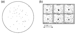
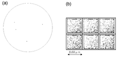
- FIG. 1A LPD was detected even though the silicon wafer was cut from a defect-free silicon single crystal. Therefore, in order to investigate the actual state of the detected LPD, the surface of the mirror-polished wafer I was observed using a scanning electron microscope (SEM).
- FIG. 1B shows six observation results of typical defect shapes observed. As shown in FIG. 1B, the observed LPD shape was found to be a pit-like defect.
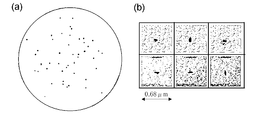
- FIG. 2A shows the detected LPD map in the wafer surface
- FIG. 2B shows the observation result of the surface of the mirror-polished wafer II by SEM.
- FIG. 2A it was confirmed that LPD was generated on the surface of the mirror polished wafer II.
- FIG. 2B it was found that the shape of the LPD detected at this time was a convex hillock. From this difference in shape, it was found that the cause of LPD formation in the mirror-polished wafer II is different from that in the mirror-polished wafer I.
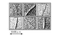
- FIG. 4 The observation result by SEM of a typical PID formed on the mirror-polished wafer IV is shown in FIG. As shown in FIG. 4, the shape of the PID was an elongated line. This clearly shows that the defects of the mirror polished wafers I and II are different from those of the PID.
- Example 5 Re-polishing of mirror-polished wafer I
- the LPD formed on the mirror-polished wafer I of Experimental Example 1 is clearly different from the cavity defect (COP) shown in Experimental Example 3 from detailed shape observation by SEM.
- polishing process shown in Experimental example 4 was shown.
- the mirror-polished wafer I was re-polished to obtain a mirror-polished wafer V, and the LPD of the mirror-polished wafer V was measured again.
- the re-polishing was performed with a polishing amount of 1.5 ⁇ m.
- the LPD map after re-polishing is shown in FIG.
- the mirror-polished wafer V has the same irregular pit-like defects as those of the mirror-polished wafer I.
- the pit-like defects are caused by the polishing process. It was confirmed that it was not a thing.
- Example 6 Repolishing of mirror polished wafer II
- the LPD formed on the mirror-polished wafer II in Experimental Example 2 is clearly different from the cavity defect (COP) shown in Experimental Example 3 from detailed shape observation by SEM. Moreover, the defect shape different from PID by the influence of the grinding
- the mirror-polished wafer II was re-polished to give a mirror-polished wafer VI, and the LPD of the mirror-polished wafer VI was measured again. .
- the re-polishing was performed with a polishing amount of 1.5 ⁇ m.
- FIG. 6A shows the LPD map after re-polishing
- FIG. 6A shows the LPD map after re-polishing
- FIGS. 6 (a) and 6 (b) show the confirmation result of the defect shape by SEM.
- the mirror-polished wafer VI had the same irregular convex hillocks as the mirror-polished wafer II. From this, it was confirmed that the PLD defect of the mirror polished wafer II was not caused by the polishing process.
- the heat treatment atmosphere was a nitrogen atmosphere
- the heat treatment temperature was 1000 ° C.
- the time was 60 minutes.
- Table 1 shows the results when impurities were measured again on the heat-treated mirror-polished wafer I by the WSA method and compared with a normal product. Among various heavy metal impurities, Cu was detected at about one digit higher concentration. In Table 1, ND indicates that it is below the detection limit.
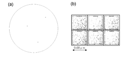
- the silicon wafer shown in Experimental Example 2 was heat-treated in a nitrogen atmosphere at 500 ° C. for 6 hours. Thereafter, the surface was repolished by 1.5 ⁇ m to prepare a mirror polished wafer VIII, and LPD measurement was performed with a particle counter.
- the LPD measurement result is shown in FIG. 8A, and the defect observation result by SEM is shown in FIG. 8B.
- LPD was significantly reduced compared to FIG. 2 (a).
- the hillock-like defect was lose
- the LPD was sufficiently reduced at the heat treatment temperature of 500 ° C., but the number of LPDs was 102 / wafer at the heat treatment temperature of 400 ° C. As a result, the effect of reducing the LPD was insufficient. This is presumably because the diffusion rate of Ni in the silicon wafer was relatively slow, and the heat treatment temperature of less than 500 ° C. did not sufficiently move to the silicon wafer surface.
- the LPD was 6 / wafer sufficiently low after the heat treatment and re-polishing. This is thought to be because the diffusion rate of Cu in the silicon wafer is very fast, easily moves to the surface of the silicon wafer, and can be removed by re-polishing.
- the heat treatment temperature is set to 500 ° C. or higher in order to avoid re-heat treatment and re-polishing.
- the heat processing temperature shall be 600 degrees C or less.
- Example 10 LPD reduction effect when heat treatment time is changed
- the heat treatment temperature was 500 ° C.
- the re-polishing amount was 1.5 ⁇ m
- the heat treatment time was 4 levels of 3 hours, 4 hours, 6 hours, and 8 hours.
- Table 4 shows the measurement results of the number of LPDs of each mirror-polished wafer after the heat treatment step and the re-polishing step.
- the LPD was sufficiently reduced in the heat treatment time of 4 hours or more and up to 8 hours, but the number of LPDs was 68 under the condition of the heat treatment time of 3 hours. / Wafer and LPD reduction effect was insufficient. Further, in the mirror polished wafer I of Experimental Example 1, even when the heat treatment time was 3 hours, the LPD was a low value of 4 pieces / wafer.
- the heat treatment time is set to 4 hours or longer so that re-heat treatment and re-polishing are not necessary.
- the heat treatment time exceeds 6 hours, the process time becomes long and the production efficiency decreases.
- the heat treatment time is longer than 6 hours, it greatly affects the precipitation characteristics of interstitial oxygen in the silicon wafer. That is, it adversely affects BMD (Bulk Micro Defect) characteristics. If BMD is formed in the vicinity of the wafer surface due to excessive oxygen precipitation, it may cause a leak in the semiconductor element formation process thereafter. Therefore, in the present invention, the heat treatment time is set to 6 hours or less in order to avoid these problems.
- the re-polishing amount is set to 1.5 ⁇ m or more so as not to be additionally re-polished.
- the heavy metal is gathered near the surface of the silicon wafer after mirror polishing without reducing the yield, and the LPD is reduced by removing it by the repolishing process.
- a method can reduce microLPD having a size of about 45 nm, which could not be removed in the past, due to heavy metal contamination during crystal growth that causes LPD.
- the present inventors have found that even if a defect-free silicon single crystal is contaminated with heavy metals at the time of growth, LPD is reduced to the limit, and a silicon wafer with a low defective product generation rate in the inspection process and the shipping stage is obtained.
- the present inventors have found a method of manufacturing a silicon wafer that can be manufactured with a high yield. The present invention will be described below.
- the present invention is a method for producing a silicon wafer from a defect-free silicon single crystal grown by the CZ method, After preparing a silicon wafer sliced from the defect-free silicon single crystal and mirror-polished, A heat treatment step of heat-treating the mirror-polished silicon wafer at a temperature of 500 ° C. or more and 600 ° C. or less for 4 hours or more and 6 hours or less;
- the silicon wafer manufacturing method is characterized by performing a re-polishing step of re-polishing the silicon wafer after the heat treatment step so that the polishing amount becomes 1.5 ⁇ m or more.
- the defect-free silicon single crystal can be grown by the CZ method, particularly by the MCZ method to which a magnetic field is applied.
- the defect-free silicon single crystal means a silicon single crystal composed of the entire N-region having no void type defect, OSF, or dislocation cluster.
- a silicon single crystal has an excess of interstitial silicon point defects caused by the presence of excess silicon atoms in the V-region where there are excessive vacancy-type point defects caused by a shortage of silicon atoms.
- grow-in defects FPD, LSTD, COP, etc.
- the concentration of these two point defects is determined from the relationship between the crystal pulling rate (growth rate) V in the CZ method and the temperature gradient G in the vicinity of the solid-liquid interface in the crystal. Since the parameter V / G determines the total concentration of point defects, a crystal with an N-region extending across the entire lateral surface can be manufactured by adjusting the pulling speed so that V / G becomes a predetermined value. It is known that the crystal of the entire N-region can be expanded in the length direction by maintaining the pulling speed when the N-region spreads horizontally.
- the defect-free silicon single crystal in the present invention is a silicon single crystal of the entire N-region grown in this way.
- a defect-free silicon single crystal is sliced, and the sliced wafer is mirror-polished to prepare a silicon wafer.
- This wafer processing step is not particularly limited, and any of the generally performed steps can be applied. In particular, after slicing, chamfering, lapping, etching, and mirror polishing are typical, but other processes may be used. Although not particularly limited, it is preferable to prepare a silicon wafer having a diameter of 300 mm or more as a sliced and mirror-polished silicon wafer. Even for a large-diameter wafer used for such a state-of-the-art product, a high-quality silicon wafer with reduced LPD can be produced by performing the heat treatment step and the re-polishing step of the present invention.
- the mirror-polished silicon wafer is heat-treated at a temperature of 500 ° C. or more and 600 ° C. or less for 4 hours or more and 6 hours or less.
- a relatively low temperature heat treatment process utilizing the high diffusion rate of heavy metals, particularly Cu and Ni, in the silicon single crystal, Cu and Ni are brought into the vicinity of the surface of the silicon wafer after mirror polishing. Can be assembled.
- the heat treatment furnace to be used is not particularly limited, and it is efficient if a vertical or horizontal batch furnace is used.
- the heat treatment temperature is set to 500 ° C. or higher so that no additional heat treatment is required in consideration of the contamination state of which heavy metal is contaminated, and the heat from the wafer support part during the heat treatment.
- the temperature is set to 600 ° C. or lower.
- the heat treatment time is set to 4 hours or more so that no additional heat treatment is required, and 6 hours so as not to adversely affect the production efficiency and BMD characteristics. The following.
- the silicon wafer after the heat treatment step is re-polished so that the polishing amount becomes 1.5 ⁇ m or more.
- the polishing amount is set to 1.5 ⁇ m or more so that additional re-polishing is not necessary.
- the polishing method can be any polishing method generally used for silicon wafers, and is not particularly limited. For example, CMP using colloidal silica as an abrasive can be performed.
- the LPD is reduced to the limit, and in the inspection process and the shipping stage when manufacturing the silicon wafer The defective product generation rate is reduced, and a silicon wafer manufacturing method with a good yield is obtained.
- the silicon wafer having 10 / wafer or less LPD having a particle size of 37 nm to 120 nm detected by a particle counter can be produced.
- LPD is reduced, a silicon wafer having a lower defect generation rate in the inspection process and the shipping stage can be manufactured with a high yield.
- the silicon wafer produced by the silicon wafer manufacturing method has an LPD reduced to the utmost even when a defect-free silicon single crystal is contaminated with heavy metal during growth, and the defective product generation rate in the inspection process and the shipping stage.
- the process confirmation wafer used in the most advanced semiconductor element manufacturing process and a silicon wafer optimal for manufacturing highly integrated semiconductor elements are obtained.
- a silicon wafer obtained by heat-treating a mirror-polished silicon wafer and re-polished wherein the number of LPDs having a particle size of 37 nm to 120 nm detected by a particle counter is 10 / wafer or less.
- a wafer can be obtained.
- the LPD is reduced to the limit, the defective product generation rate is low in the inspection process and the shipping stage, and the process confirmation wafer used in the most advanced semiconductor element manufacturing process
- the silicon wafer is suitable for manufacturing highly integrated semiconductor devices.
- the diameter of the said silicon wafer is 300 mm or more.
- Such a state-of-the-art large-diameter wafer is an optimal silicon wafer for manufacturing a process confirmation wafer used in a semiconductor element manufacturing process or a highly integrated semiconductor element.
- Example 1 A quartz crucible with a diameter of 810 mm is filled with 410 kg of polycrystalline silicon, and a defect-free silicon single crystal with a diameter of 300 mm is grown by controlling the temperature gradient (G) and growth rate (V) of the solid / liquid layer boundary region of silicon. did. At this time, boron was doped so that the specific resistance was 10 ⁇ ⁇ cm, and the crystal axis orientation was ⁇ 100>.
- the defect-free silicon single crystal was sliced, chamfered, lapped, etched, and mirror-polished to produce a mirror-polished wafer. This mirror-polished wafer was heat-treated in a nitrogen atmosphere at a heat treatment temperature of 500 ° C.
- Example 2 A mirror-polished wafer produced in the same manner as in Example 1 was heat-treated at a heat treatment temperature of 600 ° C. and a heat treatment time of 4 hours, and re-polished to a re-polishing amount of 1.5 ⁇ m to produce a silicon wafer.
- Table 6 shows the detection results of LPD.
- Example 3 A mirror-polished wafer produced in the same manner as in Example 1 was heat-treated at a heat treatment temperature of 500 ° C. and a heat treatment time of 6 hours, and re-polished to a re-polishing amount of 1.5 ⁇ m to produce a silicon wafer.
- Table 6 shows the detection results of LPD.
- Example 4 A mirror-polished wafer produced in the same manner as in Example 1 was heat-treated at a heat treatment temperature of 500 ° C. and a heat treatment time of 4 hours, and re-polished to a re-polishing amount of 2.0 ⁇ m to produce a silicon wafer.
- Table 6 shows the detection results of LPD.
- Example 1 A mirror-polished wafer produced in the same manner as in Example 1 was heat-treated at a heat treatment temperature of 400 ° C. and a heat treatment time of 4 hours, and re-polished to a re-polishing amount of 1.5 ⁇ m to produce a silicon wafer.
- Table 6 shows the detection results of LPD.
- Example 2 A mirror-polished wafer produced in the same manner as in Example 1 was heat-treated at a heat treatment temperature of 700 ° C. and a heat treatment time of 4 hours, and re-polished to a re-polishing amount of 1.5 ⁇ m to produce a silicon wafer.
- Table 6 shows the detection results of LPD.
- Example 3 A mirror-polished wafer produced in the same manner as in Example 1 was heat-treated at a heat treatment temperature of 500 ° C. and a heat treatment time of 3 hours, and re-polished to a re-polishing amount of 1.5 ⁇ m to produce a silicon wafer.
- Table 6 shows the detection results of LPD.
- Example 4 A mirror-polished wafer produced in the same manner as in Example 1 was heat-treated at a heat treatment temperature of 500 ° C. and a heat treatment time of 8 hours, and re-polished to a re-polishing amount of 1.5 ⁇ m to produce a silicon wafer.
- Table 6 shows the detection results of LPD.
- Example 5 A mirror-polished wafer produced in the same manner as in Example 1 was heat-treated at a heat treatment temperature of 500 ° C. and a heat treatment time of 4 hours, and re-polished to a re-polishing amount of 1.0 ⁇ m to produce a silicon wafer.
- Table 6 shows the detection results of LPD.
- Examples 1 to 4 of the present invention heat treatment at a relatively low temperature of 500 to 600 ° C. for 4 to 6 hours is performed by utilizing the high diffusion rate of heavy metals, particularly Cu and Ni, in a silicon single crystal.
- heavy metals can be gathered in the vicinity of the surface of the silicon wafer after mirror polishing, and further, by removing this by a re-polishing process with a polishing amount of 1.5 ⁇ m or more, LPD can be reduced. It was shown that it can be done.
- the silicon wafer of the present invention is used, the LPD is reduced to the limit, the defective product generation rate is low in the inspection process and the shipping stage, the wafer for process confirmation used in the state-of-the-art semiconductor device manufacturing process, and a highly integrated wafer It becomes a silicon wafer most suitable for the manufacture of semiconductor elements.
- the present invention is not limited to the above embodiment.
- the above-described embodiment is an exemplification, and the present invention has substantially the same configuration as the technical idea described in the claims of the present invention, and any device that exhibits the same function and effect is the present invention. It is included in the technical scope of the invention.
Landscapes
- Chemical & Material Sciences (AREA)
- Engineering & Computer Science (AREA)
- Crystallography & Structural Chemistry (AREA)
- Materials Engineering (AREA)
- Metallurgy (AREA)
- Organic Chemistry (AREA)
- Physics & Mathematics (AREA)
- Condensed Matter Physics & Semiconductors (AREA)
- General Physics & Mathematics (AREA)
- Manufacturing & Machinery (AREA)
- Computer Hardware Design (AREA)
- Microelectronics & Electronic Packaging (AREA)
- Power Engineering (AREA)
- Thermal Sciences (AREA)
- Crystals, And After-Treatments Of Crystals (AREA)
- Testing Or Measuring Of Semiconductors Or The Like (AREA)
Priority Applications (2)
| Application Number | Priority Date | Filing Date | Title |
|---|---|---|---|
| KR1020137033445A KR101905826B1 (ko) | 2011-06-20 | 2012-05-14 | 실리콘 웨이퍼 및 그 제조 방법 |
| US14/122,356 US9337013B2 (en) | 2011-06-20 | 2012-05-14 | Silicon wafer and method for producing the same |
Applications Claiming Priority (2)
| Application Number | Priority Date | Filing Date | Title |
|---|---|---|---|
| JP2011-135891 | 2011-06-20 | ||
| JP2011135891A JP5682471B2 (ja) | 2011-06-20 | 2011-06-20 | シリコンウェーハの製造方法 |
Publications (1)
| Publication Number | Publication Date |
|---|---|
| WO2012176370A1 true WO2012176370A1 (ja) | 2012-12-27 |
Family
ID=47422235
Family Applications (1)
| Application Number | Title | Priority Date | Filing Date |
|---|---|---|---|
| PCT/JP2012/003121 Ceased WO2012176370A1 (ja) | 2011-06-20 | 2012-05-14 | シリコンウェーハ及びその製造方法 |
Country Status (4)
| Country | Link |
|---|---|
| US (1) | US9337013B2 (enExample) |
| JP (1) | JP5682471B2 (enExample) |
| KR (1) | KR101905826B1 (enExample) |
| WO (1) | WO2012176370A1 (enExample) |
Cited By (1)
| Publication number | Priority date | Publication date | Assignee | Title |
|---|---|---|---|---|
| CN104749802A (zh) * | 2013-12-30 | 2015-07-01 | 三星显示有限公司 | 制造显示装置的方法 |
Families Citing this family (8)
| Publication number | Priority date | Publication date | Assignee | Title |
|---|---|---|---|---|
| WO2015186288A1 (ja) * | 2014-06-02 | 2015-12-10 | 株式会社Sumco | シリコンウェーハおよびその製造方法 |
| DE102015224933A1 (de) * | 2015-12-11 | 2017-06-14 | Siltronic Ag | Monokristalline Halbleiterscheibe und Verfahren zur Herstellung einer Halbleiterscheibe |
| JP6920849B2 (ja) | 2017-03-27 | 2021-08-18 | 株式会社荏原製作所 | 基板処理方法および装置 |
| EP3728704B1 (en) | 2017-12-21 | 2023-02-01 | GlobalWafers Co., Ltd. | Method of treating a single crystal silicon ingot to improve the lls ring/core pattern |
| JP6933187B2 (ja) * | 2018-05-01 | 2021-09-08 | 信越半導体株式会社 | 半導体シリコンウェーハの金属不純物除去方法 |
| JP7279682B2 (ja) * | 2020-04-17 | 2023-05-23 | 信越半導体株式会社 | シリコンウェーハの評価方法 |
| JP7251516B2 (ja) * | 2020-04-28 | 2023-04-04 | 信越半導体株式会社 | ウェーハの欠陥領域の判定方法 |
| KR102661941B1 (ko) * | 2021-10-14 | 2024-04-29 | 에스케이실트론 주식회사 | 웨이퍼의 결함 영역의 평가 방법 |
Citations (2)
| Publication number | Priority date | Publication date | Assignee | Title |
|---|---|---|---|---|
| JP2006004983A (ja) * | 2004-06-15 | 2006-01-05 | Shin Etsu Handotai Co Ltd | シリコンウエーハの製造方法及びシリコンウエーハ |
| JP2011014645A (ja) * | 2009-06-30 | 2011-01-20 | Covalent Materials Corp | シリコンウエハの熱処理方法 |
Family Cites Families (8)
| Publication number | Priority date | Publication date | Assignee | Title |
|---|---|---|---|---|
| JP2521007B2 (ja) | 1992-06-30 | 1996-07-31 | 九州電子金属株式会社 | シリコン単結晶の製造方法 |
| IT1280041B1 (it) | 1993-12-16 | 1997-12-29 | Wacker Chemitronic | Procedimento per il tiraggio di un monocristallo di silicio |
| JP3575644B2 (ja) | 1995-08-28 | 2004-10-13 | 三菱住友シリコン株式会社 | シリコンウェーハの製造方法 |
| US20020185053A1 (en) | 2001-05-24 | 2002-12-12 | Lu Fei | Method for calibrating nanotopographic measuring equipment |
| JP2009212354A (ja) * | 2008-03-05 | 2009-09-17 | Sumco Corp | シリコン基板の製造方法 |
| JP5446160B2 (ja) * | 2008-07-31 | 2014-03-19 | 株式会社Sumco | 再生シリコンウェーハの製造方法 |
| EP2722423B1 (en) * | 2009-03-25 | 2017-01-11 | Sumco Corporation | Method of manufacturing a silicon wafer |
| US8877643B2 (en) | 2009-06-05 | 2014-11-04 | Sumco Corporation | Method of polishing a silicon wafer |
-
2011
- 2011-06-20 JP JP2011135891A patent/JP5682471B2/ja active Active
-
2012
- 2012-05-14 WO PCT/JP2012/003121 patent/WO2012176370A1/ja not_active Ceased
- 2012-05-14 KR KR1020137033445A patent/KR101905826B1/ko active Active
- 2012-05-14 US US14/122,356 patent/US9337013B2/en active Active
Patent Citations (2)
| Publication number | Priority date | Publication date | Assignee | Title |
|---|---|---|---|---|
| JP2006004983A (ja) * | 2004-06-15 | 2006-01-05 | Shin Etsu Handotai Co Ltd | シリコンウエーハの製造方法及びシリコンウエーハ |
| JP2011014645A (ja) * | 2009-06-30 | 2011-01-20 | Covalent Materials Corp | シリコンウエハの熱処理方法 |
Cited By (3)
| Publication number | Priority date | Publication date | Assignee | Title |
|---|---|---|---|---|
| CN104749802A (zh) * | 2013-12-30 | 2015-07-01 | 三星显示有限公司 | 制造显示装置的方法 |
| US20150187637A1 (en) * | 2013-12-30 | 2015-07-02 | Samsung Display Co., Ltd. | Manufacturing method for display device |
| US9362159B2 (en) * | 2013-12-30 | 2016-06-07 | Samsung Display Co., Ltd. | Manufacturing method for display device |
Also Published As
| Publication number | Publication date |
|---|---|
| JP5682471B2 (ja) | 2015-03-11 |
| JP2013004825A (ja) | 2013-01-07 |
| KR101905826B1 (ko) | 2018-10-08 |
| KR20140046420A (ko) | 2014-04-18 |
| US9337013B2 (en) | 2016-05-10 |
| US20140103492A1 (en) | 2014-04-17 |
Similar Documents
| Publication | Publication Date | Title |
|---|---|---|
| JP5682471B2 (ja) | シリコンウェーハの製造方法 | |
| KR100581047B1 (ko) | 실리콘 단결정 웨이퍼의 제조방법 및 실리콘 단결정 웨이퍼 | |
| KR101389058B1 (ko) | 실리콘 웨이퍼 및 그 제조방법 | |
| KR100573473B1 (ko) | 실리콘 웨이퍼 및 그 제조방법 | |
| KR100788988B1 (ko) | 에피텍셜 웨이퍼용 실리콘 단결정 웨이퍼, 에피텍셜웨이퍼 및 이들의 제조방법 그리고 평가방법 | |
| KR101272659B1 (ko) | 실리콘 단결정의 제조 방법, 실리콘 단결정 잉곳 및 실리콘 웨이퍼 | |
| TWI548785B (zh) | 矽晶圓及其製造方法 | |
| JP2002187794A (ja) | シリコンウェーハおよびこれに用いるシリコン単結晶の製造方法 | |
| JP4854936B2 (ja) | シリコンウエーハの製造方法及びシリコンウエーハ | |
| KR20210037655A (ko) | 실리콘 웨이퍼의 품질 평가 방법, 실리콘 웨이퍼의 제조 방법 및 실리콘 웨이퍼 | |
| JP3589119B2 (ja) | エピタキシャルウェーハの製造方法 | |
| KR100566824B1 (ko) | 실리콘 반도체기판 및 그의 제조방법 | |
| JP4196602B2 (ja) | エピタキシャル成長用シリコンウエーハ及びエピタキシャルウエーハ並びにその製造方法 | |
| KR100854673B1 (ko) | 어닐링된 웨이퍼를 제조하는 방법 | |
| JP6493105B2 (ja) | エピタキシャルシリコンウェーハ | |
| JP4092993B2 (ja) | 単結晶育成方法 | |
| JP4089137B2 (ja) | シリコン単結晶の製造方法およびエピタキシャルウェーハの製造方法 | |
| JP2004119446A (ja) | アニールウエーハの製造方法及びアニールウエーハ | |
| JP5282762B2 (ja) | シリコン単結晶の製造方法 | |
| CN109509704B (zh) | 外延硅晶片的制备方法 | |
| JP2004221435A (ja) | 半導体ウエーハの製造方法及び半導体ウエーハ | |
| JP2007073594A (ja) | エピタキシャルシリコンウェーハの製造方法 | |
| JP5012721B2 (ja) | シリコンエピタキシャルウェーハ | |
| JP2002134513A (ja) | シリコンウェーハの熱処理方法 | |
| JP2009035481A (ja) | シリコン単結晶ウエーハ |
Legal Events
| Date | Code | Title | Description |
|---|---|---|---|
| 121 | Ep: the epo has been informed by wipo that ep was designated in this application |
Ref document number: 12803406 Country of ref document: EP Kind code of ref document: A1 |
|
| WWE | Wipo information: entry into national phase |
Ref document number: 14122356 Country of ref document: US |
|
| ENP | Entry into the national phase |
Ref document number: 20137033445 Country of ref document: KR Kind code of ref document: A |
|
| NENP | Non-entry into the national phase |
Ref country code: DE |
|
| 122 | Ep: pct application non-entry in european phase |
Ref document number: 12803406 Country of ref document: EP Kind code of ref document: A1 |