WO2012173162A1 - 量子ナノドット、二次元量子ナノドットアレイ及びこれを用いた半導体装置並びに製造方法 - Google Patents
量子ナノドット、二次元量子ナノドットアレイ及びこれを用いた半導体装置並びに製造方法 Download PDFInfo
- Publication number
- WO2012173162A1 WO2012173162A1 PCT/JP2012/065172 JP2012065172W WO2012173162A1 WO 2012173162 A1 WO2012173162 A1 WO 2012173162A1 JP 2012065172 W JP2012065172 W JP 2012065172W WO 2012173162 A1 WO2012173162 A1 WO 2012173162A1
- Authority
- WO
- WIPO (PCT)
- Prior art keywords
- quantum
- dimensional
- quantum nanodot
- nanodot
- layer
- Prior art date
- Legal status (The legal status is an assumption and is not a legal conclusion. Google has not performed a legal analysis and makes no representation as to the accuracy of the status listed.)
- Ceased
Links
Images
















Classifications
-
- B—PERFORMING OPERATIONS; TRANSPORTING
- B82—NANOTECHNOLOGY
- B82Y—SPECIFIC USES OR APPLICATIONS OF NANOSTRUCTURES; MEASUREMENT OR ANALYSIS OF NANOSTRUCTURES; MANUFACTURE OR TREATMENT OF NANOSTRUCTURES
- B82Y10/00—Nanotechnology for information processing, storage or transmission, e.g. quantum computing or single electron logic
-
- H—ELECTRICITY
- H10—SEMICONDUCTOR DEVICES; ELECTRIC SOLID-STATE DEVICES NOT OTHERWISE PROVIDED FOR
- H10D—INORGANIC ELECTRIC SEMICONDUCTOR DEVICES
- H10D48/00—Individual devices not covered by groups H10D1/00 - H10D44/00
- H10D48/383—Quantum effect devices, e.g. of devices using quantum reflection, diffraction or interference effects
-
- B—PERFORMING OPERATIONS; TRANSPORTING
- B82—NANOTECHNOLOGY
- B82Y—SPECIFIC USES OR APPLICATIONS OF NANOSTRUCTURES; MEASUREMENT OR ANALYSIS OF NANOSTRUCTURES; MANUFACTURE OR TREATMENT OF NANOSTRUCTURES
- B82Y20/00—Nanooptics, e.g. quantum optics or photonic crystals
-
- B—PERFORMING OPERATIONS; TRANSPORTING
- B82—NANOTECHNOLOGY
- B82Y—SPECIFIC USES OR APPLICATIONS OF NANOSTRUCTURES; MEASUREMENT OR ANALYSIS OF NANOSTRUCTURES; MANUFACTURE OR TREATMENT OF NANOSTRUCTURES
- B82Y40/00—Manufacture or treatment of nanostructures
-
- H—ELECTRICITY
- H01—ELECTRIC ELEMENTS
- H01S—DEVICES USING THE PROCESS OF LIGHT AMPLIFICATION BY STIMULATED EMISSION OF RADIATION [LASER] TO AMPLIFY OR GENERATE LIGHT; DEVICES USING STIMULATED EMISSION OF ELECTROMAGNETIC RADIATION IN WAVE RANGES OTHER THAN OPTICAL
- H01S5/00—Semiconductor lasers
- H01S5/30—Structure or shape of the active region; Materials used for the active region
- H01S5/34—Structure or shape of the active region; Materials used for the active region comprising quantum well or superlattice structures, e.g. single quantum well [SQW] lasers, multiple quantum well [MQW] lasers or graded index separate confinement heterostructure [GRINSCH] lasers
- H01S5/341—Structures having reduced dimensionality, e.g. quantum wires
- H01S5/3412—Structures having reduced dimensionality, e.g. quantum wires quantum box or quantum dash
-
- H—ELECTRICITY
- H01—ELECTRIC ELEMENTS
- H01S—DEVICES USING THE PROCESS OF LIGHT AMPLIFICATION BY STIMULATED EMISSION OF RADIATION [LASER] TO AMPLIFY OR GENERATE LIGHT; DEVICES USING STIMULATED EMISSION OF ELECTROMAGNETIC RADIATION IN WAVE RANGES OTHER THAN OPTICAL
- H01S5/00—Semiconductor lasers
- H01S5/30—Structure or shape of the active region; Materials used for the active region
- H01S5/34—Structure or shape of the active region; Materials used for the active region comprising quantum well or superlattice structures, e.g. single quantum well [SQW] lasers, multiple quantum well [MQW] lasers or graded index separate confinement heterostructure [GRINSCH] lasers
- H01S5/343—Structure or shape of the active region; Materials used for the active region comprising quantum well or superlattice structures, e.g. single quantum well [SQW] lasers, multiple quantum well [MQW] lasers or graded index separate confinement heterostructure [GRINSCH] lasers in AIIIBV compounds, e.g. AlGaAs-laser, InP-based laser
-
- H—ELECTRICITY
- H10—SEMICONDUCTOR DEVICES; ELECTRIC SOLID-STATE DEVICES NOT OTHERWISE PROVIDED FOR
- H10D—INORGANIC ELECTRIC SEMICONDUCTOR DEVICES
- H10D48/00—Individual devices not covered by groups H10D1/00 - H10D44/00
- H10D48/30—Devices controlled by electric currents or voltages
-
- H—ELECTRICITY
- H10—SEMICONDUCTOR DEVICES; ELECTRIC SOLID-STATE DEVICES NOT OTHERWISE PROVIDED FOR
- H10D—INORGANIC ELECTRIC SEMICONDUCTOR DEVICES
- H10D62/00—Semiconductor bodies, or regions thereof, of devices having potential barriers
- H10D62/80—Semiconductor bodies, or regions thereof, of devices having potential barriers characterised by the materials
- H10D62/81—Semiconductor bodies, or regions thereof, of devices having potential barriers characterised by the materials of structures exhibiting quantum-confinement effects, e.g. single quantum wells; of structures having periodic or quasi-periodic potential variation
- H10D62/812—Single quantum well structures
- H10D62/814—Quantum box structures
-
- H—ELECTRICITY
- H10—SEMICONDUCTOR DEVICES; ELECTRIC SOLID-STATE DEVICES NOT OTHERWISE PROVIDED FOR
- H10F—INORGANIC SEMICONDUCTOR DEVICES SENSITIVE TO INFRARED RADIATION, LIGHT, ELECTROMAGNETIC RADIATION OF SHORTER WAVELENGTH OR CORPUSCULAR RADIATION
- H10F10/00—Individual photovoltaic cells, e.g. solar cells
-
- H—ELECTRICITY
- H10—SEMICONDUCTOR DEVICES; ELECTRIC SOLID-STATE DEVICES NOT OTHERWISE PROVIDED FOR
- H10F—INORGANIC SEMICONDUCTOR DEVICES SENSITIVE TO INFRARED RADIATION, LIGHT, ELECTROMAGNETIC RADIATION OF SHORTER WAVELENGTH OR CORPUSCULAR RADIATION
- H10F10/00—Individual photovoltaic cells, e.g. solar cells
- H10F10/10—Individual photovoltaic cells, e.g. solar cells having potential barriers
- H10F10/17—Photovoltaic cells having only PIN junction potential barriers
- H10F10/172—Photovoltaic cells having only PIN junction potential barriers comprising multiple PIN junctions, e.g. tandem cells
-
- H—ELECTRICITY
- H10—SEMICONDUCTOR DEVICES; ELECTRIC SOLID-STATE DEVICES NOT OTHERWISE PROVIDED FOR
- H10F—INORGANIC SEMICONDUCTOR DEVICES SENSITIVE TO INFRARED RADIATION, LIGHT, ELECTROMAGNETIC RADIATION OF SHORTER WAVELENGTH OR CORPUSCULAR RADIATION
- H10F10/00—Individual photovoltaic cells, e.g. solar cells
- H10F10/10—Individual photovoltaic cells, e.g. solar cells having potential barriers
- H10F10/19—Photovoltaic cells having multiple potential barriers of different types, e.g. tandem cells having both PN and PIN junctions
-
- H—ELECTRICITY
- H10—SEMICONDUCTOR DEVICES; ELECTRIC SOLID-STATE DEVICES NOT OTHERWISE PROVIDED FOR
- H10F—INORGANIC SEMICONDUCTOR DEVICES SENSITIVE TO INFRARED RADIATION, LIGHT, ELECTROMAGNETIC RADIATION OF SHORTER WAVELENGTH OR CORPUSCULAR RADIATION
- H10F77/00—Constructional details of devices covered by this subclass
- H10F77/10—Semiconductor bodies
- H10F77/14—Shape of semiconductor bodies; Shapes, relative sizes or dispositions of semiconductor regions within semiconductor bodies
- H10F77/143—Shape of semiconductor bodies; Shapes, relative sizes or dispositions of semiconductor regions within semiconductor bodies comprising quantum structures
- H10F77/1433—Quantum dots
-
- H—ELECTRICITY
- H01—ELECTRIC ELEMENTS
- H01S—DEVICES USING THE PROCESS OF LIGHT AMPLIFICATION BY STIMULATED EMISSION OF RADIATION [LASER] TO AMPLIFY OR GENERATE LIGHT; DEVICES USING STIMULATED EMISSION OF ELECTROMAGNETIC RADIATION IN WAVE RANGES OTHER THAN OPTICAL
- H01S2304/00—Special growth methods for semiconductor lasers
-
- H—ELECTRICITY
- H10—SEMICONDUCTOR DEVICES; ELECTRIC SOLID-STATE DEVICES NOT OTHERWISE PROVIDED FOR
- H10K—ORGANIC ELECTRIC SOLID-STATE DEVICES
- H10K85/00—Organic materials used in the body or electrodes of devices covered by this subclass
- H10K85/761—Biomolecules or bio-macromolecules, e.g. proteins, chlorophyl, lipids or enzymes
-
- H—ELECTRICITY
- H10—SEMICONDUCTOR DEVICES; ELECTRIC SOLID-STATE DEVICES NOT OTHERWISE PROVIDED FOR
- H10P—GENERIC PROCESSES OR APPARATUS FOR THE MANUFACTURE OR TREATMENT OF DEVICES COVERED BY CLASS H10
- H10P50/00—Etching of wafers, substrates or parts of devices
- H10P50/69—Etching of wafers, substrates or parts of devices using masks for semiconductor materials
- H10P50/691—Etching of wafers, substrates or parts of devices using masks for semiconductor materials for Group V materials or Group III-V materials
- H10P50/692—Etching of wafers, substrates or parts of devices using masks for semiconductor materials for Group V materials or Group III-V materials characterised by their composition, e.g. multilayer masks or materials
-
- H—ELECTRICITY
- H10—SEMICONDUCTOR DEVICES; ELECTRIC SOLID-STATE DEVICES NOT OTHERWISE PROVIDED FOR
- H10P—GENERIC PROCESSES OR APPARATUS FOR THE MANUFACTURE OR TREATMENT OF DEVICES COVERED BY CLASS H10
- H10P50/00—Etching of wafers, substrates or parts of devices
- H10P50/71—Etching of wafers, substrates or parts of devices using masks for conductive or resistive materials
-
- H—ELECTRICITY
- H10—SEMICONDUCTOR DEVICES; ELECTRIC SOLID-STATE DEVICES NOT OTHERWISE PROVIDED FOR
- H10P—GENERIC PROCESSES OR APPARATUS FOR THE MANUFACTURE OR TREATMENT OF DEVICES COVERED BY CLASS H10
- H10P76/00—Manufacture or treatment of masks on semiconductor bodies, e.g. by lithography or photolithography
- H10P76/40—Manufacture or treatment of masks on semiconductor bodies, e.g. by lithography or photolithography of masks comprising inorganic materials
- H10P76/405—Manufacture or treatment of masks on semiconductor bodies, e.g. by lithography or photolithography of masks comprising inorganic materials characterised by their composition, e.g. multilayer masks
-
- Y—GENERAL TAGGING OF NEW TECHNOLOGICAL DEVELOPMENTS; GENERAL TAGGING OF CROSS-SECTIONAL TECHNOLOGIES SPANNING OVER SEVERAL SECTIONS OF THE IPC; TECHNICAL SUBJECTS COVERED BY FORMER USPC CROSS-REFERENCE ART COLLECTIONS [XRACs] AND DIGESTS
- Y02—TECHNOLOGIES OR APPLICATIONS FOR MITIGATION OR ADAPTATION AGAINST CLIMATE CHANGE
- Y02E—REDUCTION OF GREENHOUSE GAS [GHG] EMISSIONS, RELATED TO ENERGY GENERATION, TRANSMISSION OR DISTRIBUTION
- Y02E10/00—Energy generation through renewable energy sources
- Y02E10/50—Photovoltaic [PV] energy
- Y02E10/548—Amorphous silicon PV cells
Definitions
- the present invention relates to a quantum nanodot, a two-dimensional quantum nanodot array, a semiconductor device using these, and a manufacturing method. More specifically, the present invention relates to a quantum nanodot having high uniformity of about 10 nm or less, a high-density two-dimensional quantum nanodot array in which the quantum nanodots are arranged two-dimensionally, and a quantum nanodot of the two-dimensional quantum nanodot array.
- the present invention relates to a two-dimensional quantum nanodot array in which an intermediate layer made of a semiconductor or an insulator is filled in between and which can control light absorption characteristics and carrier transport characteristics, and further relates to a semiconductor device and a manufacturing method using the same.
- An exposure of 22 nm has been put into practical use as a minimum processing dimension in fine processing of a semiconductor integrated circuit.
- an electron beam or a focused ion beam (FIB) is used for processing up to about 10 nm.
- processing using an electron beam or FIB processing of 10 nm or less is considered difficult.
- Such a processing method is a method of reducing the size by cutting from above, and is called a so-called top-down technique.
- a material corresponding to the Bohr radius of excitons (excitons) in a semiconductor behaves as a quantum dot due to three-dimensional quantum confinement of carriers, and further exhibits a quantum size effect.
- the quantum size effect can control the band gap energy (Eg) by changing the size of the quantum dots.
- Minibands occur in multiple quantum dots. This miniband is closely tied to the confined energy level.
- the layer arranged between a plurality of quantum dots is called an intermediate layer.
- SiC is a promising material for the intermediate layer.
- a mini-band can be easily formed in the intermediate layer made of SiC and the solar cell made of Si quantum dots.
- the present inventors have produced quantum dots made of Si or GaAs using ferritin, which is a protein containing a metal, to produce quantum dots of about 12 nm (see Non-Patent Documents 5 and 6).
- quantum dots having a size on the order of nm, particularly smaller than 10 nm by a conventional technique such as a plasma process involving lithography and a sputtering technique involving annealing. Further, a flexible process is required for a semiconductor device using different quantum dot materials and quantum nanodots such as Si and a compound semiconductor, but has not yet been realized.
- an object of the present invention is to provide a quantum nanodot having a dimension of about 10 nm or less, a two-dimensional quantum nanodot array, a semiconductor device using the same, and a manufacturing method, which have been difficult with conventional methods. .
- the inventor of the present invention uses a monolayer of a protein containing a metal having a diameter of several nanometers in a two-dimensional direction, and further prevents defects in a semiconductor or the like that becomes a quantum nanodot, so that It is possible to form quantum nanodots, control quantum confinement effects such as diameter and thickness of quantum nanodots, control light absorption characteristics and light emission, and directly control light emission and emission wavelength from Si quantum nanodots. Observed ahead of the world and reached the present invention.
- the quantum nanodot of the present invention is made of a semiconductor, and the outer diameter in the two-dimensional direction is not more than twice the Bohr radius of excitons in the semiconductor.
- the semiconductor is preferably Si, and the outer diameter in the two-dimensional direction is 10 nm or less.
- the quantum nanodot of the present invention can emit light.
- the quantum nanodot of the present invention preferably has an emission peak at 665 nm having a half-width of about 0.2 eV in photoluminescence characteristics excited at 400 nm.
- the quantum nanodot can preferably control the quantum confinement effect by changing the thickness and the dimension in the two-dimensional direction.
- the surface density of the quantum nanodot is preferably 1 ⁇ 10 12 / cm 2 to 5 ⁇ 10 12 / cm 2 .
- the quantum nanodot is made of a semiconductor, and the outer diameter in the two-dimensional direction is not more than twice the Bohr radius of excitons in the semiconductor, A large number of these quantum nanodots are uniformly arranged in two dimensions, and the interval between the quantum nanodots is 1 nm to 10 nm.
- the semiconductor is preferably Si, and the outer diameter in the two-dimensional direction is 10 nm or less.
- the quantum nanodot preferably emits light.
- Quantum nanodots preferably have a 665 nm emission peak half-width of about 0.2 eV in the photoluminescence properties excited at 400 nm.
- the surface density of the quantum nanodot is preferably 1 ⁇ 10 12 / cm 2 to 5 ⁇ 10 12 / cm 2 .
- an intermediate layer made of a semiconductor or an insulator is filled between the two-dimensional quantum nanodot arrays.
- the transport characteristics of the two-dimensional quantum nanodot array are controlled by the distance between adjacent quantum nanodots.
- the optical absorption characteristics and carrier transport characteristics of the two-dimensional quantum nanodot array are controlled by the distance between adjacent quantum nanodots.
- the intermediate layer is preferably made of a semiconductor or an insulator having a band gap larger than that of the quantum nanodot.
- the intermediate layer is preferably any of SiO 2 , Si 3 O 4 , and SiC.
- the transport properties of the two-dimensional quantum nanodot array are controlled by the intermediate layer and the distance between adjacent quantum nanodots.
- the optical absorption properties of the two-dimensional quantum nanodot array can be controlled by the intermediate layer and the distance between adjacent quantum nanodots.
- a semiconductor device of the present invention includes the two-dimensional quantum nanodot array described in any of the above.
- the semiconductor device is preferably a solar cell.
- the solar cell is preferably composed of at least a two-dimensional quantum nanodot array and includes two or more layers having different band gap energies.
- a plurality of two-dimensional quantum nanodot arrays having the same band gap may be stacked.
- the semiconductor device is preferably a semiconductor laser, and the active layer of the semiconductor laser is composed of a two-dimensional quantum nanodot array.
- the method for producing a two-dimensional quantum nanodot array of the present invention comprises a protein encapsulating a metal whose outer diameter in the two-dimensional direction is not more than twice the Bohr radius of excitons in a semiconductor.
- Two-dimensionally arranged quantum nanodots consisting of semiconductor layers, formed in a two-dimensional direction on a semiconductor layer to be quantum nanodots, etched with proteins, and etched with a compound containing a metal exposed by etching as a mask And a compound containing a metal is etched.
- the metal-encapsulating protein is preferably Listeria ferritin.
- the semiconductor layer is preferably deposited using neutral particles.
- the semiconductor layer is preferably etched using neutral particles.
- a layer serving as an intermediate layer is deposited on the two-dimensional quantum nanodot formed after etching the compound containing metal.
- the quantum nanodot of the present invention has a high quantum confinement effect because the dimension in the two-dimensional direction is not more than twice the Bohr radius of excitons in a semiconductor, and is highly oriented and dense. For this reason, quantum nanodots made of Si generate direct transitional light emission.
- the two-dimensional quantum nanodot array of the present invention has a dimension in the two-dimensional direction that is not more than twice the Bohr radius of excitons in a semiconductor, is highly oriented, and has a high density. Good characteristics.
- an efficient semiconductor device can be obtained due to the quantum confinement effect.
- a two-dimensional quantum nanodot array smaller than about 10 nm can be produced with high orientation and high density using a protein containing a metal as a template.
- FIG. 1A is a plan view
- FIG. 1B is a cross-sectional view taken along line II in FIG.
- FIG. 1A is a plan view
- FIG. 1B is a cross-sectional view taken along line II in FIG.
- FIG. 1A is a plan view
- FIG. 1B is a cross-sectional view taken along line II in FIG.
- It is an expanded sectional view of the quantum nanodot of FIG.
- FIG. 1B is a cross-sectional view taken along line II in FIG.
- FIG. 1A is a plan view
- FIG. 1B is a cross-sectional view taken along line II in FIG.
- FIG. 1A is a plan view
- FIG. 1B is a cross-sectional view taken along line II in FIG.
- FIG. 1A is a plan view
- FIG. 1B is a cross-sectional view taken along line II in FIG.
- FIG. 1A is a plan view
- FIG. 1B is a cross-sectional
- FIG. 6 is a band diagram of the two-dimensionally arranged quantum nanodot array of FIG. 5. It is a specific example of a band diagram in which quantum nanodots are Si and various intermediate layers are used, and the intermediate layers are (a) SiO 2 , (b) Si 3 O 4 , and (c) SiC.
- (A) shows the cross section of the two-dimensional quantum nanodot array structure which has an intermediate
- (b) has shown typical IV characteristic for demonstrating the transport characteristic. It is a figure explaining the light absorption characteristic of the two-dimensional quantum nanodot array structure which has an intermediate
- FIG. 12 It is sectional drawing which shows the structure of the semiconductor laser diode using the two-dimensional quantum nanodot array which has an intermediate
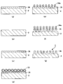
- A)-(h) is a figure which shows sequentially the manufacturing method of a two-dimensional quantum nanodot array.
- the two-dimensional Si quantum nanodot array having (c) shows the case of the two-dimensional Si quantum nanodot array having the intermediate layer made of the SiO 2 film of the embodiment. It is a graph which shows a Tauc plot, (a) is a SiC film having a thickness of 5 nm, (b) is a two-dimensional Si quantum nanodot array having an intermediate layer made of the SiC film of the example, and (c) is SiO of the example. A case of a two-dimensional Si quantum nanodot array having an intermediate layer composed of two films is shown. It is a graph which compares the measurement result of the absorption coefficient of the quantum nanodot array arranged two-dimensionally, (a) is an example and (b) is a comparative example.
- (A)-(g) is a figure which shows sequentially the manufacturing method of the two-dimensional quantum nanodot array which consists of GaAs. It is PL spectrum of GaAs after performing NB etching and the conventional plasma etching. It is a scanning electron microscope image of the surface of the listeria ferritin arranged two-dimensionally on the NB oxide film formed in GaAs. It is the FTIR spectrum figure which measured the GaAs surface after an oxygen radical process by the Fourier spectroscopy. It is a figure of the scanning electron microscope image which shows the cross section after carrying out NB etching of GaAs. It is a figure of the scanning electron microscope image in the surface of the GaAs quantum nanodot array arranged two-dimensionally.
- a film composed of a 3 nm SiO 2 layer and Si quantum nanodots shows a case of a single SiC layer having a thickness of 5 nm.
- (a) is IV characteristic
- (b) is a figure which shows the space probability of an electron. It is a graph which shows the measurement result of the light absorption coefficient of a solar cell, (a) is a solar cell which has a 2 nm-thick SiC layer and Si quantum nanodot with a thickness of 4 nm, (b) is thickness. The case of a solar cell having a 2 nm SiC layer is shown. It is a figure which shows IV characteristic of a solar cell. It is a figure which shows the relationship between the wavelength of a solar cell, and external quantum efficiency.
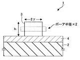
- FIG. 1A and 1B are diagrams showing the configuration of a two-dimensionally arranged quantum nanodot array 1 according to the present invention, where FIG. 1A is a plan view and FIG. 1B is a cross-sectional view taken along line II in FIG. .
- FIG. 2 is a schematic enlarged cross-sectional view of the quantum nanodot 3 of FIG.
- two-dimensionally arranged quantum nanodots hereinafter abbreviated as two-dimensional quantum nanodots
- Each quantum nanodot 3 is made of a semiconductor and has a dimension that causes a quantum effect.
- the semiconductor a material made of an inorganic material or an organic material can be used.
- the inorganic semiconductor include single element semiconductors such as Si and Ge, compound semiconductors, mixed crystals of a plurality of compound semiconductors, and the like.
- the substrate 2 a substrate material capable of forming the quantum nanodots 3 on the surface of the substrate 2 can be used.
- the above-described semiconductor substrate 2 or a substrate 2 made of glass or quartz glass may be used.
- a substrate in which an insulating film 4 such as an oxide film is formed on a semiconductor substrate 2 may be used.
- the quantum nanodot 3 has a dimension in the two-dimensional direction that is not more than twice the Bohr radius of excitons in the semiconductor.
- the quantum nanodot 3 has a thickness in a direction perpendicular to the two-dimensional direction.
- the semiconductor is Si
- the exciton Bohr radius in Si is about 5 nm.
- the Bohr radius of excitons in Si is also simply referred to as Bohr radius.
- FIG. 3 is a diagram showing the dimensions of the quantum nanodot 3.
- the quantum nanodot 3 has dimensions of Lx, Ly, and Lz in the xyz direction.
- the z direction is the thickness direction of the cross-sectional structure shown in FIG.
- the energy of electrons of the quantum nanodot 3 shown in FIG. 3 is expressed by the following formula (1) (see Non-Patent Document 7).
- n, m, and l are quantum numbers
- h bar is Planck's constant / 2 ⁇
- m * is an effective mass of a semiconductor forming the quantum nanodot 3.
- the electron energy can be obtained if Lx, Ly, and Lz are determined.
- the dimension of the quantum nanodot is referred to as an outer diameter.
- the outer diameter is a diameter when the area shape of the quantum nanodot is approximated by a circle.
- Quantum nanodots are arranged at intervals of 1 nm to 10 nm.
- the quantum nanodot 3 is made of Si, light can be emitted when the diameter in the two-dimensional direction is 6 nm to 10 nm.
- a direct transition type and an Auger effect type are conceivable as described later.
- the direct transition type that is, direct transition light emission is a transition approaching a direct transition.
- FIG. 4 is an energy band structure illustrating direct transition and indirect transition. As shown in FIG. 4, the direct transition is a vertical transition in the k space.
- heat and sound which are unnecessary energy for light emission, are also changed, that is, lattice vibration is involved, so light is not emitted efficiently.
- the surface density of the quantum nanodot 3 can be set to 1 ⁇ 10 12 / cm 2 to 5 ⁇ 10 12 / cm 2 .
- the surface density can be adjusted by changing the interval between the quantum nanodots in the range of 1 nm to 10 nm.
- quantum nanodots are formed of Si, for example, in the photoluminescence characteristics excited at 400 nm, the half-width of the 665 nm emission peak is about 0.2 eV.
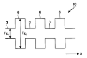
- FIG. 5A and 5B are diagrams showing another technical configuration of the two-dimensionally arranged quantum nanodot array, in which FIG. 5A is a plan view and FIG. 5B is a cross-sectional view taken along line II-II in FIG.
- the two-dimensional quantum nanodot array 10 shown in FIG. 5 differs from the two-dimensional quantum nanodot array 1 shown in FIG. 1 in that an intermediate layer 6 is disposed between the quantum nanodots 3.
- the intermediate layer 6 is made of a semiconductor or an insulator.
- the intermediate layer 6 may be a semiconductor or an insulator having a band gap larger than that of the quantum nanodot 3.
- the intermediate layer 6 may be, for example, any one of SiO 2 , Si 3 O 4 , and SiC.
- layers composed of the quantum nanodots 3 may be formed in multiple layers.
- optical absorption characteristics and transport characteristics of the two-dimensional quantum nanodot array 10 are controlled by the intermediate layer 6 and the distance between adjacent quantum nanodots 3.
- FIG. 6 is a band diagram of the two-dimensional quantum nanodot array 10 of FIG.
- FIG. 6 is a band diagram when the layer composed of the quantum nanodots 3 of the two-dimensional quantum nanodot array 10 is formed in multiple layers.
- FIG. 6 shows a case where the band gap of the intermediate layer 6 is larger than the band gap of the quantum nanodot 3, the band gap of the quantum nanodot 3 is Eg 1 , and the band gap of the intermediate layer 6 is Eg 2 .
- FIG. 7 is a specific example of a band diagram in which the quantum nanodot 3 is Si and various intermediate layers 6 are used.
- the intermediate layers 6 are (a) SiO 2 , (b) Si 3 O 4 , and (c) SiC, respectively. This case is shown.
- FIG. 7 shows a case where the band gap of the intermediate layer 6 is larger than the band gap of the quantum nanodot 3, the band gap of the quantum nanodot 3 is Eg 1 , and the band gap of the intermediate layer 6 is Eg 2 .
- the band gap of Si is 1.1 eV
- the band gaps of SiC, Si 3 N 4 , and SiO 2 are 2.5 eV, 5.3 eV, and 9 eV, respectively.
- the two-dimensional quantum nanodot array 10 having the intermediate layer 6 has a so-called superlattice structure.
- the two-dimensional quantum nanodot array 15 having the intermediate layer 6 is also referred to as a superlattice quantum nanodot layer.
- FIG. 8 is a diagram for explaining the transport characteristics of the two-dimensional quantum nanodot array structure 15 having the intermediate layer 6, where (a) shows the structure and (b) shows the schematic IV characteristics of (a). Show.
- the two-dimensionally arranged quantum nanodot array structure 15 in FIG. 8A is a diode, and a two-dimensional quantum nanodot array 10 having an intermediate layer 6 is formed on the n-type substrate 2.
- a structure in which a p layer 7 is formed on the intermediate layer 6 is shown.
- the quantum nanodot array 10 is made of Si
- the n-type substrate 2 and the p layer 7 can be similarly formed of Si.
- the IV characteristic changes depending on the interval S between adjacent quantum nanodots 3, that is, the width of the intermediate layer 6 inserted between adjacent quantum nanodots 3. Show.
- the interval S is shortened, the current easily flows, that is, the transport characteristics are improved.
- the transport characteristics are further improved by direct tunnel injection.
- the transport properties can also be changed by the material of the intermediate layer 6.
- the electrical conductivity is higher than that in the case where the intermediate layer 6 is made of SiO 2 and the transport characteristics are improved. .
- the two-dimensional quantum nanodot array 10 is combined with the distance between the intermediate layer 6 and the adjacent quantum nanodot 3 and the band gap of the material forming the intermediate layer 6.
- the transport characteristics of the are controlled.
- the improvement of carrier transport characteristics depends on how the wave functions overlap between quantum dots. That is, when the distance between the quantum nanodots is shortened and the intermediate layer 6 having a small band gap is used, the wave functions of the quantum nanodots 3 overlap to form a miniband. As a result, the tunnel movement of the carriers formed by the quantum nanodots 3 is promoted, and the carrier transport characteristics are promoted.
- the interval between the quantum nanodots is shortened, a single electron tunnel effect is generated, that is, a Coulomb brocade is generated, and the voltage for this is also lowered.
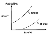
- FIG. 9 is a diagram for explaining the light absorption characteristics of the two-dimensional quantum nanodot array 10 having the intermediate layer 6.
- the light absorption characteristics can be increased by changing the material of the intermediate layer 6 from SiO 2 to SiC, for example. .
- SiO 2 , Si 3 O 4 , SiC, or the like for the region between the quantum nanodots 3, that is, the intermediate layer 6 or the interlayer, it is possible to control light absorption and carrier transport characteristics.
- FIG. 10 is a perspective view showing the structure of the solar cell 20 formed by two-dimensionally arranging the quantum nanodot array 10 having the intermediate layer 6 of the present invention.
- the solar cell 20 includes a first solar cell layer 21 made of Si, a second solar cell layer 22 formed on the first solar cell layer 21, and a second solar cell.
- the n-layer electrode 25 is formed.
- the first solar cell layer 21 is a so-called pin diode in which a p layer 21a, an i layer 21b, and an n layer 21c made of Si are sequentially stacked, and a band gap (Eg) is 1.1 eV, Responds to about 1100 nm.
- the second solar cell layer 22 includes a p layer 22a formed on the n layer 21c, a first superlattice quantum nanodot layer 22b formed on the p layer 22a, and a first superlattice quantum nanodot layer 22b.
- the n layer 22c is formed on the top.
- the configuration of the second solar cell layer 22 is such that the i layer 21b of the first solar cell layer 21 is a first superlattice quantum nanodot layer 22b having a band gap different from that of the i layer 21b. is there.
- the band gap (Eg) of the quantum nanodot 3 in the first superlattice quantum nanodot layer 22b is 1.5 eV, and the wavelength responds to about 800 nm.
- the band gap (Eg) of the quantum nanodot 3 can be controlled by adjusting the size of the quantum nanodot 3 as described above.
- the first superlattice quantum nanodot layer 22b is composed of a two-dimensional quantum nanodot array having a single layer structure including the quantum nanodots 3 and the intermediate layer 6 shown in FIG.
- the first superlattice quantum nanodot layer 22b may be formed by stacking a plurality of two-dimensional quantum nanodot arrays having the same band gap. That is, a structure in which a plurality of, for example, 5 to 10 layers of two-dimensional quantum nanodot arrays having a single layer structure are stacked may be used.
- the configuration of the third solar cell layer 23 is the same as the configuration of the second solar cell layer 22.
- the third solar cell layer 23 includes a p layer 23a formed on the n layer 22c of the second solar cell layer 22, a second superlattice quantum nanodot layer 23b formed on the p layer 23a, And n layer 23c formed on two superlattice quantum nanodot layers 23b.
- the band gap (Eg) of the quantum nanodot 3 in the second superlattice quantum nanodot layer 23b is 2 eV and responds to a wavelength of about 600 nm.
- the band gap (Eg) of the quantum nanodot 3 can be controlled by adjusting the size of the quantum nanodot 3 as described above.
- the second superlattice quantum nanodot layer 23b is composed of a two-dimensional quantum nanodot array having a single layer structure including the quantum nanodots 3 and the intermediate layer 6 shown in FIG.
- the second superlattice quantum nanodot layer 23b may be formed by stacking a plurality of two-dimensional quantum nanodot arrays having the same band gap. That is, a structure in which a plurality of, for example, 5 to 10 layers of two-dimensional quantum nanodot arrays having a single layer structure are stacked may be used.
- the n-layer electrode 25 formed on the uppermost layer of the third solar cell layer 23 may be further covered with a protective film 26.
- the protective film 26 is preferably a light transmissive material.
- a transparent electrode such as an oxide made of indium and tin (Indium Tin Oxide, hereinafter referred to as ITO) can be used.
- the solar cell 20 described above is a so-called tandem type in which a pin type first solar cell layer 21, a second solar cell layer 22, and a third solar cell layer 23 are connected in series. It has a solar cell structure.
- Each of these layers 21, 22, and 23 corresponds to about 1100 nm, about 800 nm, and about 600 nm, so that electrons and holes are efficiently formed in the infrared region and the visible light region of sunlight.
- the intermediate layer 6 of the first and second superlattice quantum nanodot layers allows electrons and holes generated by sunlight irradiation to be efficiently transported to the electrode.
- the intermediate layer 6 is made of, for example, SiC, and the interval between the quantum nanodots 3 may be set to an interval on the order of nm so that tunnel injection is likely to occur. This interval is, for example, 2 nm to 6 nm, preferably 3 nm or less.
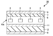
- FIG. 11 is a cross-sectional view showing the structure of a semiconductor laser diode 30 using the two-dimensionally arranged quantum nanodot array 10 of the present invention.
- An intermediate layer 6 is filled between the quantum nanodots 3.
- the semiconductor laser diode 30 using the two-dimensional quantum nanodot array 10 having the intermediate layer 6 includes an n layer 11 formed on the substrate 2 and a two-dimensional arrangement formed on the n layer 11.
- the active layer composed of the quantum nanodot array 10a and the p-layer 7 formed on the two-dimensionally arranged quantum nanodot array 10 are sequentially included.
- An n layer electrode 8 is formed on the substrate 2 side, and a p layer electrode 9 is formed on the p layer 7.
- the two-dimensional quantum nanodot array 10 having the intermediate layer 6 operates as the active layer 10a.
- the quantum nanodot 3 can be made of GaAs and the intermediate layer 6 can be made of AlGaAs.
- the interval between the quantum nanodots 3 is preferably 6 to 10 nm so that a miniband is not realized in the active layer 10a.
- an n-type cladding layer is provided between the n layer 11 and the active layer 10a, and a p-type cladding layer is provided between the p layer 7 and the active layer 10a. It may be provided.
- the n-type and p-type cladding layers are made of a material having a larger band gap than the n-layer 11 and the p-layer 7.
- FIG. 12 is a diagram illustrating a method of manufacturing the two-dimensional quantum nanodot arrays 1 and 10 in the order of steps.
- a semiconductor layer 31 is formed on the substrate 2.
- the semiconductor layer 31 is described as a poly-Si layer.
- a 3 nm surface oxide film (SiO 2 ) 32 is deposited on the poly-Si layer 31 by an apparatus using neutral particles developed by the present inventor (see Patent Document 1).
- NB Neutral Beam
- a protein 33 containing a metal is deposited two-dimensionally on SiO 2 32. Since the size of the quantum nanodot 3 is determined by the size of the metal encapsulated in the protein, a protein encapsulating the metal is used so that the quantum nanodot 3 of 10 nm or less can be obtained.
- the protein encapsulating the metal is, for example, Listeria ferritin 33.
- Listeria ferritin 33 is a complex composed of a protein and a metal, and is also called a bioconjugate.
- hemoglobin is composed of four proteins including a heme group in which an iron oxide (Fe 2 O 3 ) core is bonded to the center of a cyclic compound called porphyrin.
- Listeria ferritin is obtained by culturing in E. coli.
- the iron oxide (Fe 2 O 3 ) core is also simply called an iron core.
- Etching is performed by NF 3 gas / hydrogen radical treatment to remove SiO 2 32 on the surface, and poly Si 31 is removed by NB etching.
- SiO 2 32 is isotropically etched by NF 3 gas / hydrogen radical treatment using the iron oxide core 34a as a mask, the dimensions of the SiO 2 32 below the iron oxide core 34a are changed when the etching time is changed. Can be changed.
- anisotropic (vertical) NB etching may be performed using the iron oxide core 34a and the SiO 2 32 as a mask. In this step, the shape of the mask is transferred as Si quantum nanodots.
- the anisotropic etching can be performed by a neutral particle beam (NB) using chlorine.
- NB neutral particle beam
- the etching rate of the silicon oxide film is slow, but further etching is performed.
- the dimension of the quantum nanodot 3 can be determined by the dimension of SiO 2 32. In this way, it is possible to control the dimensions of the quantum nanodot 3.
- the semiconductor used for the quantum nanodot has been described as Si, but it can also be applied to a compound semiconductor such as GaAs.
- the following steps are performed after the steps (a) to (f).
- the material of the intermediate layer 6 will be described as SiC.
- the surface SiO 2 layer is removed by NF 3 treatment or the like.
- SiC thicker than the quantum nanodot 3 is deposited on the Si quantum dots by sputtering or the like.
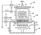
- FIG. 13 is a diagram illustrating a configuration of a deposition apparatus 40 using neutral particles.
- a neutral particle beam generating unit 60 is provided, for example, in the upper part of the reaction chamber 50.
- a support base 54 on which a semiconductor wafer 53 to be processed is placed is provided.
- the support base 54 has a temperature control device (not shown), and the semiconductor wafer 53 is controlled to a predetermined temperature.
- the reaction chamber 50 has a gas inlet 55 and an exhaust mechanism 56. The inside of the reaction chamber 50 is maintained at a predetermined pressure by the exhaust mechanism 56, and the source gas is guided from the gas inlet 55 onto the semiconductor wafer 53 on the support base 54. If an etching gas is used as the source gas, the deposition apparatus 40 using neutral particles becomes an etching apparatus.
- the neutral particle beam generator 60 has a plasma chamber 62 made of, for example, quartz.
- a gas inlet 67 is provided in the upper part of the plasma chamber 62, and a gas used for the reaction is introduced into the plasma chamber 62 from the gas inlet 67.
- a coil 68 is wound around the plasma chamber 62. One end of the coil 68 is grounded, and the other end is connected to a high frequency power source 69.
- An anode electrode 70 as an upper electrode is provided in the upper part inside the plasma chamber 62.
- the anode electrode 70 is connected to a direct current power source 71 and a high frequency power source 69.
- a cathode electrode 72 as a lower electrode is provided at a boundary portion between the lower portion of the plasma chamber 62 and the reaction chamber 50.
- the cathode electrode 72 is connected to a DC power source 73 for bias through a switch SW.
- the DC power source 73 is a variable power source, and the DC power source 73 can change the electric field between the anode electrode 70 and the cathode electrode 72.
- the DC power source 73 may be connected to a bias low frequency power source 74 via a switch SW.
- the cathode electrode 72 is made of carbon, for example, and has a plurality of openings 72a.
- the opening 72 a has an aspect ratio (ratio between the thickness of the cathode electrode 72 and the diameter of the opening 72 a) in a range of, for example, 10 or more and 20 or less, and an opening ratio (a plurality of surface areas of the cathode electrode 72 with respect to the surface area).
- the ratio of the opening area by the opening 72a) is set to a range of, for example, 50% or less and 30% or more.
- the cathode electrode 72 neutralizes and passes positive charged particles, and blocks electrons, UV light, or photons generated from the plasma.
- a pressure difference between the reaction chamber 50 and the plasma chamber 62 is provided.
- the pressure in the reaction chamber 50 is set to 100 mmTorr or more, for example, and the pressure in the plasma chamber 62 is set to 1 Torr or more, for example.
- the iron oxide core 34a was removed by NB etching.
- the formed quantum nanodots made of Si had a thickness of 4 nm, a diameter of 6 to 7 nm, and an average interval between the quantum nanodots of 12.2 nm. The size distribution of these quantum nanodots was 8.3%.
- the iron oxide core 34a was removed by wet etching with HCl.
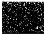
- FIG. 14A and 14B are diagrams of a scanning electron microscope image of the two-dimensionally arranged quantum nanodot array 10 having the intermediate layer 6 manufactured by the manufacturing method shown in FIG. 12, where FIG. 14A shows the surface, and FIG. 14B shows the cross section. ing. An enlarged SEM image is also inserted in the lower left of FIG. As apparent from FIG.
- the diameter of each quantum nanodot 3 is 6.4 nm
- the surface density of the quantum nanodot 3 is Was 1.2 ⁇ 10 12 / cm 2
- the SiO 2 layer 32, the Si quantum nanodots 3 and the intermediate layer 6 are formed on the substrate. It can be seen that the diameter and thickness of the Si quantum nanodots 3 are uniform, and the intermediate layer 6 is formed between and above the Si quantum nanodots 3.
- FIG. 15 is a diagram of a scanning electron microscopic image of the surface of a two-dimensionally arranged quantum nanodot array 10 having an intermediate layer 6 produced using conventional ferritin.
- the surface density of the quantum nanodot 3 is 7 ⁇ 10. 11 / cm 2 .
- the quantum nanodots 3 in the quantum nanodot array 10 having the intermediate layer 6 and two-dimensionally arranged produced by the above-described manufacturing method are highly oriented and have a high density.
- high orientation means that the sizes of the quantum nanodots 3 themselves are uniform, and the interval between the quantum nanodots 3, that is, the interval in the two-dimensional direction of the intermediate layer 6 is the same.
- the high density of the quantum nanodots 3 means that the surface density of the quantum nanodots 3 is 1 ⁇ 10 12 / cm 2 or more.
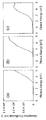
- FIG. 16 is a diagram showing measurement results of the time-resolved photoluminescence method, where (a) is a PL spectrum, (b) is an attenuation characteristic of the PL spectrum of (a), and (c) is an enlarged view of the PL spectrum. is there. As shown in FIGS.
- a photoluminescence spectrum (also referred to as a PL spectrum) is obtained from the quantum nanodot array 10 having the intermediate layer 6 and two-dimensionally arranged, and the center wavelength is 665 nm ( 1.85 eV).
- the full width at half maximum of this spectrum was 0.2 eV. This value was found to be significantly narrower than the half-value width (0.5 eV) (see Non-Patent Documents 8 and 9) of a conventional Si nanocrystal or a sample prepared by self-assembly by thermal annealing or ion implantation.
- 0.1 eV has recently been reported as the half-width of the PL spectrum of a Si nanocrystal composed of a single crystal (see Non-Patent Document 10).
- FIG. 17 is a diagram showing the attenuation characteristics of the time-resolved photoluminescence method, (a) shows high-density quantum nanodots of the example, and (b) shows a comparative example.
- a comparative example is a low-density quantum nanodot. As is clear from FIG. 17, it has been found that the lifetime of light emission from the low-density quantum nanodots is longer than that in the example.
- the remarkably narrow half-width of the PL spectrum obtained in the example is that the Si quantum nanodots 3 are composed of uniform dimensions and shapes, and are not indirect transitions as in bulk Si but directly transitional. This indicates that a transition is occurring.
- FIG. 18 is a graph showing the thickness dependence of the Si quantum nanodot 3 with respect to the photon energy at the peak wavelength of the PL spectrum.
- the horizontal axis of FIG. 18 is the thickness (nm) of the Si quantum nanodot 3, and the vertical axis is the photon energy (eV) of the PL spectrum peak wavelength.
- the photon energies when the thickness of the Si quantum nanodot 3 is 4 nm, 6 nm, and 8 nm were about 1.78 eV, 1.82 eV, and 1.85 eV, respectively. From this, it was found that the peak wavelength of the PL spectrum can be changed by changing the thickness of the Si quantum nanodot 3.
- FIG. 19 is a graph showing the diameter dependence of the quantum nanodot 3 with respect to the band gap.
- the horizontal axis in FIG. 19 is the diameter of the quantum nanodot 3 made of Si and the thickness (nm) of the natural oxide film, and the vertical axis is the band gap energy (eV) obtained from the PL spectrum.
- the band gap energy (eV) obtained from the PL spectrum.
- the band gap of the Si quantum nanodot 3 of the example having a diameter of about 6 nm is about 2 eV.
- the band gaps of the Si quantum nanodots of the comparative example having diameters of about 10.5 nm and 12.5 nm were about 1.9 eV and 1.8 eV, respectively. From this, the band gap of the quantum nanodot 3, that is, the state of quantum confinement, can be changed by changing the diameter of the Si quantum nanodot 3.
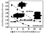
- FIG. 20 is a graph showing the thickness dependence of the quantum nanodot 3 with respect to the band gap.
- the horizontal axis of FIG. 20 is the thickness (nm) of the quantum nanodot 3 made of Si, and the vertical axis is the band gap energy (eV) obtained from the PL spectrum.
- the quantum nanodot 3 made of the conventional ferritin shown in FIG. 20 and the quantum nanodot made of polycrystalline Si having a thickness of 2 to 8 nm are also shown.
- the thickness of the Si quantum nanodot 3 of the example is 2 to 6 nm and this thickness is smaller than the Bohr radius (about 5 nm), the quantum confinement effect in the thickness and diameter directions I understand that there is.
- the thickness of the conventional Si quantum nanodot 3 is 10 nm and this thickness is larger than the Bohr radius (about 5 nm), it can be seen that there is a weak quantum confinement effect only in the diameter direction.
- the band gap of the quantum nanodot 3 that is, the quantum confinement state, by changing not only the diameter but also the thickness of the Si quantum nanodot 3 of the embodiment.
- the remarkably narrow half width of the PL spectrum obtained in the example is that the Si quantum nanodots 3 are composed of uniform dimensions and shapes, and that the obtained Si quantum nanodots 3 are free of defects. I understood. Furthermore, it has been found that direct transitional light emission can be obtained by the quantum confinement effect due to the short decay characteristics of the time-resolved photoluminescence method and the thickness dependence of the Si quantum nanodots 3.
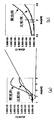
- FIG. 21 shows IV characteristics of the two-dimensional quantum nanodot array 10 having the intermediate layer 6, where (a) shows the interval between the quantum nanodots 3 of the example is 12 nm, and (b) shows the interval between the quantum nanodots of the comparative example. The case of 30 nm or more is shown. From FIG.
- the high-density Si quantum nanodot 3 of the example can obtain high conductance and non-linear IV characteristics that change stepwise.
- FIG. 21B it was found that in the Si quantum nanodot 3 of the comparative example, a current was much less likely to flow than in the example, and the conductance was low.
- the Si quantum nanodots 3 are closely arranged and coupled to the intermediate layer 6 in the plane, so in the two-dimensional quantum nanodot array 10 having the intermediate layer 6 It can be estimated that a miniband is formed.
- the absorption characteristics of the two-dimensional quantum nanodot array 10 having the produced intermediate layer 6 will be described.
- the absorption characteristics of the prepared two-dimensional quantum nanodot array 10 having the SiC intermediate layer 6 were measured using an ultraviolet-visible-near infrared (UV-Vis-FIR) spectrophotometer.
- a SiC film having a thickness of 5 nm was also measured as a comparative example.
- the absorption coefficient ( ⁇ ) at each photon energy was calculated by the following equation (2).
- I 0 is the incident light intensity
- I is the transmitted light intensity
- R the reflectance
- d the thickness of the quantum nanodot 3.
- FIG. 22 is a graph showing the measurement results of the absorption coefficient measured from the ultraviolet-visible-near-infrared spectroscopic measurement, where (a) is a SiC film with a thickness of 5 nm, and (b) is from the SiC film of the example.
- (C) shows the case of a two-dimensional Si quantum nanodot array having the intermediate layer 6 made of the SiO 2 film of the embodiment.
- the horizontal axis in FIG. 22 is photon energy (eV), and the vertical axis is the absorption coefficient (cm ⁇ 1 ).
- the thickness of both the SiC film and Si is 4 nm.
- the thickness of the SiO 2 film is 3 nm, the thickness of Si is 4 nm. 22 (b) and 22 (c), the absorption edge of the two-dimensionally arranged Si quantum nanodot array 10 of the example hardly changes.
- the two-dimensional quantum nano dot array 10 with an intermediate layer 6 made of SiC film was found that the absorption coefficient than the case of two-dimensional quantum nano dot array 10 with an intermediate layer 6 made of SiO 2 film is large.
- the large absorption coefficient of the two-dimensionally arranged quantum nanodot array 10 in which the intermediate layer 6 is made of a SiC film is due to photon absorption of the SiC film.
- the band gap (Eg) was obtained from each absorption coefficient measured in FIG. 22 by Tauc plot shown in the following equation (3).
- ⁇ is the absorption coefficient
- h is the Planck constant
- ⁇ is the photon frequency
- Eg is the bandgap energy.
- the power of the left side of equation (2), 1/2 assumes an indirect transition.
- ( ⁇ h ⁇ ) 1/2 is plotted on the Y-axis
- photon energy is plotted on the X-axis
- FIG. 23 is a graph showing a Tauc plot, where (a) is a 5 nm thick SiC film, (b) is a two-dimensional Si quantum nanodot array 10 having an intermediate layer 6 made of the SiC film of the example, (c) ) Shows the case of the two-dimensional Si quantum nanodot array 10 having the intermediate layer 6 made of the SiO 2 film of the embodiment.
- the horizontal axis of FIG. 23 is photon energy (eV), and the vertical axis is ( ⁇ h ⁇ ) 1/2 (cm ⁇ 1 eV 1/2 ).
- the thickness of both the SiC film and Si is 4 nm.
- the thickness of the SiO 2 film is 3 nm, the thickness of Si is 4 nm.
- FIG. 23A shows that the Eg of the SiC film having a thickness of 5 nm is 3.4 eV. From FIG. 23 (b), the Eg of the Si quantum nanodot array 10 having a thickness of 4 nm and having an intermediate layer 6 made of a SiC film having a thickness of 4 nm and arranged in a two-dimensional manner and having a thickness of 4 nm is 2.0 eV. I understand that.
- This value is the same value as that of the Si quantum nanodot array 10 having the intermediate layer 6 made of the SiO 2 film shown in FIG. From this, since the band gap of Si is smaller than the band gap of SiC, the band gap of the Si quantum nanodot array 10 having the intermediate layer 6 made of SiC film and two-dimensionally arranged is the structure of the quantum nanodot array 10 made of Si. It can be seen that From the above, the absorption coefficient is larger than that in the case where the intermediate layer 6 is made of SiO 2 without changing the Eg of the two-dimensionally arranged Si quantum nanodot array 10 having the intermediate layer 6 made of the SiC film of the embodiment. It turns out that you can.
- FIG. 24 is a graph comparing the absorption coefficients of the example and the comparative example of the two-dimensionally arranged quantum nanodot array 10, wherein (a) is a measured value, and (b) is a circle indicated by a dotted line in (a).
- FIG. The horizontal axis in FIG. 24 is photon energy (eV), and the vertical axis is the absorption coefficient (cm ⁇ 1 ).
- eV photon energy
- the vertical axis is the absorption coefficient (cm ⁇ 1 ).
- Listeria ferritin 33 is used, and conventional ferritin is used in the comparative example. From FIG. 24, it was found that the absorption coefficient of the example using Listeria ferritin 33 was increased by about 5 times compared to the comparative example using ferritin.
- FIGS. 25A to 25G show a method of manufacturing the two-dimensional quantum nanodot array 1 made of GaAs in the order of steps.
- a GaAs substrate 2 is prepared.
- a natural oxide film 36 is formed on the surface of the GaAs substrate 2.
- B The natural oxide film 36 on the GaAs substrate 2 was removed by hydrogen radicals. The flow rate of hydrogen was 40 sccm, and hydrogen radicals were generated by a high frequency power source of 13.56 MHz and 200 W.
- the GaAs substrate was inserted into the oxidation chamber of the NB device, and an oxide film 38 having a thickness of 1 nm was formed on the GaAs substrate at room temperature.
- This oxide film 38 is called a GaAs oxide film or an NB oxide film.
- the flow rate of oxygen was 5 sccm, and the pressure was 0.14 Pa.
- the high frequency power supply of 13.56 MHz is 500 W output.
- a two-dimensional array of Listeria ferritin 33 was deposited on SiO 2 .
- the shell of Listeria ferritin 33 was removed by oxygen radical treatment.
- a two-dimensional array 34 composed of iron oxide cores 34a is deposited on the GaAs oxide film.
- the two-dimensional array 34 composed of these iron oxide cores serves as an etching mask for the next step.
- GaAs etching was performed with NB.
- the iron oxide core 34a was removed by wet etching with HCl.
- FIG. 26 is a PL spectrum of GaAs after NB etching and conventional plasma etching.
- NB etching stripe patterns having widths of 5, 3, 1, and 0.7 ⁇ m were used.
- the comparative sample is a GaAs substrate that is not etched without a pattern.
- the horizontal axis in FIG. 26 is the stripe width ( ⁇ m), and the vertical axis is the PL spectrum intensity normalized by the PL spectrum intensity of the comparative sample.
- FIG. 26 in the case of NB etching, it was found that the PL spectrum intensity of GaAs after etching is almost the same as that before etching and does not depend on the stripe width.
- NB etching In contrast to NB etching, the PL spectrum of GaAs after conventional plasma etching increases non-radiative recombination due to damage caused by damage, and the PL spectrum intensity decreases, and the degree is more pronounced as the stripe width is narrower. (See Non-Patent Document 11). From this, it can be seen that NB etching has the advantage of not damaging the GaAs surface. Therefore, this NB etching is a method suitable for the manufacturing method of the GaAs quantum nanodot 3.
- Listeria ferritin 33 is generated from DNA information and includes a core made of uniform 7 nm iron oxide (Fe 2 O 3 ). In order to form a monomolecular layer of listeria ferritin 33 that is uniform and has a high in-plane density, the condition of the surface oxide film is an important factor. A conventional mechanism of self-assembly of ferritin has been studied (see Non-Patent Document 6). A highly hydrophilic surface can reduce the adsorptive power of Listeria ferritin 33 and can help to have sufficient freedom for movement of Listeria ferritin 33.
- the repulsive force due to the negative charge of Listeria ferritin 33 itself can help to prevent multilayering that occurs during the movement of Listeria ferritin 33.
- a monolayer of listeria ferritin 33 arranged in two dimensions with high in-plane density can be formed by self-assembly.
- the NB oxide film (GaAs-NBO) formed on the GaAs surface by the NB device described above has high hydrophilicity and a high zeta potential of ⁇ 20 mV (Non-patent Document 6).
- FIG. 27 is a scanning electron microscope image of the surface of Listeria ferritin 33 formed on an NB oxide film formed on GaAs and arranged two-dimensionally. As is clear from FIG. 27, it can be seen that Listeria ferritin 33 formed in GaAs has no vacancies.
- FIG. 28 is an FTIR spectrum obtained by measuring the GaAs surface after the oxygen radical treatment by Fourier spectroscopy.
- the horizontal axis in FIG. 28 is the wave number (cm ⁇ 1 ), and the vertical axis is the absorption rate (arbitrary scale).
- GaAs etching was performed under the following conditions. Etching conditions Etching gas: Mixed gas of chlorine (Cl 2 ) and argon (Ar) Chlorine gas flow rate: 9 sccm Argon gas flow rate: 31 sccm 13.56MHz power supply output: 800W Output of low frequency bias power supply: 16W Substrate temperature: -16 ° C
- FIG. 29 is a scanning electron microscope image of the cross section after NB etching of GaAs. As is apparent from FIG. 29, it is found that a column having a nano-order dimension made of GaAs having a high aspect ratio of 9 nm in diameter and 30 nm in depth is formed. Further, the surface on the bottom side of GaAs subjected to NB etching, that is, the etched surface was flat, and the unevenness of the etched surface was 1 nm.
- the removal of the iron oxide core was confirmed by X-ray photoelectron spectroscopy (XPS) measurement.
- XPS X-ray photoelectron spectroscopy
- FIG. 30 is a scanning electron microscope image on the surface of the two-dimensionally arranged GaAs quantum nanodot array 1. The magnification is 40,000 times. As is clear from FIG. 30, the diameter is about 7 nm. The thickness of each quantum nanodot 3 was about 10 nm, and the surface density of the quantum nanodot 3 was 7 ⁇ 10 11 / cm 2 .
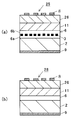
- FIGS. 31A and 31B are cross-sectional views showing the structures of the solar cells 25 and 28.
- FIG. 31A shows the structure when the Si quantum nanodot 3 is used
- FIG. 31B shows the structure when the SiC layer 6 is used alone.
- a solar cell 25 using Si quantum nanodots 3 includes a p-layer electrode 9, a substrate 2 made of p-type Si, an Si quantum nanodot 3, an intermediate layer 6, and an n-type made of n-type Si.
- the layer 11, the protective film 26, and the n-layer electrode 8 are included.
- the Si quantum nanodot 3 is formed between the first intermediate layer 6a and the second intermediate layer 6b.
- the intermediate layer 6 SiC or SiO 2 is used.
- the solar cell 25 using the Si quantum nanodot 3 is expressed as 2 nm SiC / 2 nm SiND / 2 nm.
- 2 nm SiC is the SiC layer 6 having a thickness of 2 nm
- 2 nm SiND is the Si quantum nanodot 3 having a thickness of 2 nm.
- the solar cell 28 using the SiC layer 6 includes a p-layer electrode 9, a substrate 2 made of p-type Si, an SiC layer 6, an n-layer 11 made of n-type Si, and a protective film 26.
- the n-layer electrode 8 is included.
- the solar cell 28 using the SiC layer 6 is expressed as 2 nm SiC.
- 2 nm is the thickness of the SiC layer 6.
- Solar cells 25 and 28 using the SiC layer 6 and the Si quantum nanodots 3 were manufactured as follows. Using a p substrate 2 having a thickness of 400 ⁇ m and 1.0 to 1.5 ⁇ , a two-dimensional quantum nanodot array 1 was manufactured by the method shown in FIG. The uppermost layer is the SiC layer 6. The formed two-dimensional quantum nanodot array 1 had a diameter of about 6.4 nm (see FIG. 14). On the SiC layer 6, an Si layer having a thickness of 30 nm at 600 ° C. was epitaxially grown by an electron beam evaporation method. The grown Si layer was made into an n layer 11 doped with phosphorus (P) by a diffusion method using RTA (Rapid Thermal Annealing). This layer is a very thin n + layer, also called an n emitter layer. On the n layer 11, an ITO film having a thickness of 70 nm to be the protective film 26 is formed. The ITO film 26 is a so-called transparent electrode.
- the electrode 9 is formed on the p substrate 2 with aluminum paste.
- the finger electrode 8 is formed by silver paste.
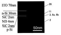
- FIG. 32 is a view showing a scanning electron microscope (SEM) image of a cross section of the solar cell 25 using the manufactured Si quantum nanodot 3.
- SEM scanning electron microscope
- FIG. 33 is a graph showing the measurement result of the absorption coefficient measured from the ultraviolet-visible-near-infrared spectroscopic measurement, wherein (a) is a film composed of the SiC layer 6 having a thickness of 3 nm and the Si quantum nanodots 3; b) shows a film composed of the SiO 2 layer 6 having a thickness of 3 nm and the Si quantum nanodot 3, and (c) shows a case of the film having only the SiC layer 6 having a thickness of 5 nm. From FIG.
- the light absorption at 2 eV to 3 eV is a film composed of the SiO 2 layer 6 and the Si quantum nanodot 3 as the intermediate layer, or the SiC layer 6 alone. It can be seen that there is a marked increase compared to the other films.
- FIG. 34 is a diagram showing the IV characteristics and (b) the electron spatial probability in the two-dimensional quantum nanodot 3 having the intermediate layer 6.
- FIG. 34A shows that when the intermediate layer 6 is made of SiC, a larger current and a lower threshold voltage can be obtained than when the intermediate layer 6 is made of SiO 2 . This is because when the intermediate layer 6 is made of SiC, the coupling of the wave function between the Si quantum nanodots 3 becomes strong, and a wide intermediate band is formed.
- FIG. 34 (b) is a diagram showing the spatial probability of electrons obtained by calculating the Schrodinger equation in the intermediate layer 6 and the three adjacent quantum nanodots 3 by the classical envelope function theory.
- the horizontal axis in the figure is the interval between the quantum nanodot arrays, and the vertical axis is the logarithmic scale electron spatial probability.
- the wave function is more easily diffused across the barrier, so that they are easily coupled to each other.
- the coupling of wave functions is stronger than in the case where the intermediate layer 6 is a SiO 2 layer, so that light absorption and carrier mobility are increased. To do.
- FIG. 35 is a graph showing the measurement results of the light absorption coefficient of the solar cells 25 and 28, in which (a) shows a solar cell having the SiC layer 6 having a thickness of 2 nm and the Si quantum nanodot 3 having a thickness of 4 nm. Batteries 25 and (b) show the case of the solar battery 28 having the SiC layer 6 having a thickness of 2 nm. From FIG. 35, in the case of the solar cell 25 having the SiC layer 6 having a thickness of 2 nm and the quantum nanodot 3 having a thickness of 4 nm, the solar cell 28 having the SiC layer 6 having a thickness of 2 nm. It was found that the light absorption characteristics are much better than
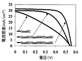
- FIG. 36 is a diagram illustrating the IV characteristics of the solar cells 25 and 28.
- the horizontal axis in FIG. 36 is the voltage (V) generated in the solar cell, and the vertical axis is the current density (mA / cm 2 ) flowing through the solar cell. From FIG. 36, in the case of the solar cell 25 having the SiC layer 6 and the Si quantum nanodot 3, the current density is larger than that of the solar cell 28 having the SiC layer 6 having a thickness of 2 nm. It turns out that it is obtained.
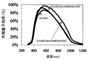
- FIG. 37 is a diagram showing the relationship between the wavelengths of the solar cells 25 and 28 and the external quantum efficiency.
- the horizontal axis in FIG. 37 is the wavelength (nm), and the vertical axis is the external quantum efficiency (%) of the solar cell. From FIG. 37, in the case of the solar cell 25 having the SiC layer 6 and the Si quantum nanodot 3, the peak of the external quantum efficiency was obtained at about 620 nm. It was found that in the solar cell 28 having the SiC layer 6 with a thickness of 2 nm, the peak of the external quantum efficiency moves to the short wavelength side, that is, blue shifts.
- Table 1 summarizes the short-circuit current density J sc (mA / cm 2 ), open-circuit voltage V oc (V), fill factor (also referred to as Fill Factor, FF), and solar cell efficiency (%) for each solar cell. Show.
- the fill factor (FF) is expressed by the following equation (4).
- V max and I max are the voltage and current at the maximum output point of the solar cell, respectively, and Isc is a short circuit current. Efficiency of the solar cell, V oc, I sc, increases in proportion to the fill factor.
- the short-circuit current density is 29.9 mA / cm 2 and the open circuit voltage is 0. .539V
- fill factor was 58%
- efficiency was 9.3%
- the short-circuit current density is 31.3 mA / cm 2
- the open-circuit voltage is 0.556 V
- the fill factor is 72%
- the efficiency is 12 It was 6%.
- the short-circuit current density is 29.0 mA / cm 2
- the open circuit voltage is 0.544 V
- the fill factor is 34%
- the efficiency of the solar cell 28 is 5. 4%.
- the solar cell 25 having the SiC layer 6 having a thickness of 2 nm and the Si quantum nanodot 3 having a thickness of 4 nm all of the short-circuit current density, the open-circuit voltage, the fill factor, and the efficiency are large. Excellent results were obtained.
- a two-dimensional quantum nanodot array having a single layer structure including the quantum nanodots 3 and the intermediate layer 6 is used.
- the solar cell Increases efficiency.
Landscapes
- Engineering & Computer Science (AREA)
- Physics & Mathematics (AREA)
- Chemical & Material Sciences (AREA)
- Nanotechnology (AREA)
- Condensed Matter Physics & Semiconductors (AREA)
- Optics & Photonics (AREA)
- General Physics & Mathematics (AREA)
- Crystallography & Structural Chemistry (AREA)
- Electromagnetism (AREA)
- Biophysics (AREA)
- Life Sciences & Earth Sciences (AREA)
- Manufacturing & Machinery (AREA)
- Mathematical Physics (AREA)
- Theoretical Computer Science (AREA)
- Photovoltaic Devices (AREA)
- Semiconductor Lasers (AREA)
Abstract
Description
上記構成において、好ましくは、半導体はSiであり、二次元方向の外径が10nm以下である。
本発明の量子ナノドットは、発光を生じ得る。本発明の量子ナノドットは、好ましくは、400nmで励起されるフォトルミネッセンス特性において、665nmの発光ピ-クの半値幅が約0.2eVである。
量子ナノドットは、好ましくは、厚さと二次元方向の寸法とを変えることで量子閉じ込め効果を制御できる。
量子ナノドットの面密度は、好ましくは、1×10¹²/cm2から5×1012/cm2である。
上記構成において、好ましくは、半導体はSiであり、二次元方向の外径が10nm以下である。
量子ナノドットは、好ましくは発光が生じる。量子ナノドットは、好ましくは、400nmで励起されるフォトルミネッセンス特性において、665nmの発光ピ-クの半値幅が約0.2eVである。
量子ナノドットの面密度は、好ましくは、1×10¹²/cm2から5×1012/cm2である。
さらに、好ましくは、二次元量子ナノドットアレイの間に半導体または絶縁体からなる中間層が充填される。
好ましくは、隣接する量子ナノドット間の距離によって二次元量子ナノドットアレイの輸送特性が制御される。
好ましくは、隣接する量子ナノドット間の距離によって二次元量子ナノドットアレイの光学吸収特性及びキャリア輸送特性が制御される。
中間層は、好ましくは、量子ナノドットよりもバンドギャップの大きい半導体又は絶縁体からなる。中間層は、好ましくは、SiO2、Si3O4、SiCの何れかである。
好ましくは、中間層と、隣接する量子ナノドット間の距離と、によって二次元量子ナノドットアレイの輸送特性が制御される。
二次元量子ナノドットアレイの光学吸収特性は、中間層と、隣接する量子ナノドット間の距離とによって制御され得る。
上記構成において、半導体装置は、好ましくは太陽電池である。太陽電池は、好ましくは、少なくとも二次元量子ナノドットアレイからなり、バンドギャップエネルギーの異なる層を2層以上備えている。また、同じバンドギャップの二次元量子ナノドットアレイを複数積層して用いてもよい。
半導体装置は、好ましくは半導体レーザであり、半導体レーザの活性層が二次元量子ナノドットアレイからなる。
上記構成において、金属を内包したタンパク質は、好ましくは、リステリアフェリチンである。
半導体層を、好ましくは、中性粒子を用いて堆積する。半導体層を、好ましくは、中性粒子を用いてエッチングする。
好ましくは、金属を含む化合物をエッチングした後に形成された二次元量子ナノドット上に、中間層となる層を堆積する。
2:基板
3:量子ナノドット
4:絶縁層
6:中間層
6a:第1の中間層
6b:第2の中間層
7:p層
8,24:n層電極
9,25:p層電極
10a:活性層
11:n層
20,25,28:太陽電池
21:第1の太陽電池層
22:第2の太陽電池層
23:第3の太陽電池層
26:保護膜
30:半導体レーザダイオード
31:ポリSi
32:SiO2膜
33:リステリアフェリチン
34:酸化鉄コアからなる二次元アレイ
34a:酸化鉄コア
36:自然酸化膜
38:GaAs酸化膜
40:中性粒子を用いた堆積装置
50:反応室
53:半導体ウェハ
54:支持台
55,67:ガス導入口
56:排気機構
60:中性粒子ビーム生成部
62:プラズマ室
68:コイル
69:高周波電源
71,73:直流電源
70:アノード電極
72:カソード電極
74:低周波電源
図1は、本発明に従う二次元配置された量子ナノドットアレイ1の構成を示す図であり、(a)は平面図、(b)は(a)のI-I線に沿った断面図である。図2は、図1の量子ナノドット3の模式的な拡大断面図である。
図1に示すように、二次元配置された量子ナノドット(以下、二次元量子ナノドットと略する。)1は基板2上に形成されている。各量子ナノドット3は半導体からなり、量子効果が生じるような寸法を有している。半導体は、無機物又は有機物からなる材料を使用できる。無機物からなる半導体としては、Si,Geのような単元素半導体や化合物半導体、複数の化合物半導体の混晶等が挙げられる。基板2としては、基板2の表面に量子ナノドット3が形成できる基板材料を使用できる。具体的には、上記の半導体の基板2やガラスや石英ガラスからなる基板2を用いてもよい。図1,図2に示すように、半導体の基板2上に酸化膜等の絶縁膜4を形成した基板を使用してもよい。
図3に示す量子ナノドット3の電子のエネルギーは、下記(1)式で表わされる(非特許文献7参照)。

n=m=l=1の基底状態においては、電子のエネルギーは、Lx,Ly,Lzが決まれば求まる。以下、明細書では、量子ナノドットの寸法を外径と呼ぶ。外径は、量子ナノドットの面積形状を円で近似したときの直径である。
図5に示す二次元量子ナノドットアレイ10が、図1の二次元量子ナノドットアレイ1と異なるのは、各量子ナノドット3の間に中間層6が配設されている点にある。中間層6は半導体又は絶縁体からなる。中間層6は、量子ナノドット3よりもバンドギャップの大きい半導体又は絶縁体としてもよい。中間層6は、例えば、SiO2、Si3O4、SiCの何れかとしてもよい。
図7は、中間層6のバンドギャップが量子ナノドット3のバンドギャップよりも大きい場合を示しており、量子ナノドット3のバンドギャップはEg1、中間層6のバンドギャップはEg2である。図7に示すように、Siのバンドギャップが1.1eVであるのに対して、SiC、Si3N4、SiO2のバンドギャップは、それぞれ2.5eV、5.3eV、9eVである。
図8(a)の二次元配置された量子ナノドットアレイ構造15はダイオードとなっており、中間層6を有している二次元量子ナノドットアレイ10が、n型の基板2上に形成され、さらに中間層6上には、p層7が形成された構造を示している。量子ナノドットアレイ10がSiからなる場合、n型の基板2及びp層7は、同様にSiで形成することができる。
図8(b)は、上記ダイオード構造15においては、隣接する量子ナノドット3間の間隔S、即ち隣接する量子ナノドット3の間に挿入される中間層6の幅によって、IV特性は変化することを示している。間隔Sを短くすると電流が流れ易くなる、つまり輸送特性が向上する。間隔Sをnmオーダーにすることで、直接トンネル注入により、さらに輸送特性が向上する。輸送特性は、中間層6の材料によっても変えることができる。Siからなる量子ナノドット3とSiCからなる中間層6とを有している二次元量子ナノドットアレイ10では、中間層6がSiO2の場合と比較して電気電導性が高く、輸送特性が向上する。
(太陽電池)
図10は、本発明の中間層6を有している量子ナノドットアレイ10を二次元配置することで形成した太陽電池20の構造を示す斜視図である。
図10に示すように、太陽電池20は、Siからなる第1の太陽電池層21と、第1の太陽電池層21上に形成される第2の太陽電池層22と、第2の太陽電池層22上に形成される第3の太陽電池層23と、さらに、第1の太陽電池層21に形成されるp層電極24と、第3の太陽電池層23の最上層となるn層23cに形成されるn層電極25とから構成されている。
図11は、本発明の二次元配置された量子ナノドットアレイ10を用いた半導体レーザダイオード30の構造を示す断面図である。量子ナノドット3の間には中間層6が充填されている。
図11に示すように、中間層6を有する二次元量子ナノドットアレイ10を用いた半導体レーザダイオード30は、基板2上に形成されるn層11と、n層11上に形成される二次元配置された量子ナノドットアレイ10aからなる活性層と、二次元配置された量子ナノドットアレイ10上に形成されるp層7と、が順に積層された層を含んで構成されている。基板2側にはn層電極8が、p層7上にはp層電極9が形成されている。
次に、本発明の二次元配置された量子ナノドットアレイ1、10の製造方法について説明する。
図12は、二次元量子ナノドットアレイ1,10の製造方法を工程順に示す図である。以下、(a)~(h)に分けて説明する。
(a)基板2上に半導体層31を形成する。以下の説明では、半導体層31をポリSi層として説明する。
(b)本発明者が開発した中性粒子を用いた装置(特許文献1参照)によって、ポリSi層31上に3nmの表面酸化膜(SiO2)32を堆積する。以下、中性粒子を用いた装置で堆積した膜をNB(Neutral Beam)膜とも呼ぶ。中性粒子を用いた装置ではエッチングも可能であり、このエッチングをNBエッチングと呼ぶ。
ここで、リステリアフェリチン33は、たんぱく質と金属とからなる複合体であり、バイオコンジュゲートとも呼ばれている。生体内では酸化鉄(Fe2O3)コアがポルフィリンという環状の化合物の中心に結合しているヘム基を含む、たんぱく質4分子からできているのがヘモグロビンである。リステリアフェリチンは大腸菌の中で培養して得られる。酸化鉄(Fe2O3)コアは、単に鉄コアとも呼ばれている。
上記した二次元量子ナノドットアレイ1における、(a)~(f)の工程の後で次の工程を行う。中間層6の材料はSiCとして説明する。
(g)表面SiO2層をNF3処理等で除去する。量子ナノドット3よりも厚いSiCを、スパッタリング等でSiの量子ドット上に堆積する。
上記工程によって、図12(h)に示すように、各量子ナノドット3の隙間に中間層6を形成し、中間層6を有する二次元量子ナノドットアレイ10を製造することができる。
下記に示す実施例により本発明をさらに詳細に説明する。
(a)酸化膜付きSi基板2又は石英基板に6nmのアモルファスSi31を、電子ビーム蒸着法によって6nm堆積した。次に、窒素雰囲気中でアニールしてポリSi31とした。
(b)中性粒子を用いた装置40(特許文献1参照)によって、ポリSi31上に厚さが3nmの表面酸化膜32(SiO2)を堆積した。
図13は、中性粒子を用いた堆積装置40の構成を示す図である。この中性粒子を用いた堆積装置40は、反応室50の例えば上部に、中性粒子ビーム生成部60が設けられている。
(d)リステリアフェリチン33のシェルを酸素雰囲気中でアニールして除去した。SiO2上には、酸化鉄コア34aからなる二次元アレイ34が堆積した状態となる。これらの酸化鉄コア34aからなる二次元アレイ34が次の工程のエッチング用マスクとなる。
(e)酸化鉄コア34aをマスクとして、最初に、表面側のSiO232をNF3ガス/水素ラジカル処理エッチングを行い、表面側のSiO232を除去した。
次に、酸化鉄コア34aをマスクとして、ポリSi31をNBエッチングで除去した。
形成されたSiからなる量子ナノドットの厚さは4nmで、直径は6~7nm、量子ナノドット間の平均間隔は12.2nmであった。これらの量子ナノドットの寸法分布は8.3%であった。
(f)酸化鉄コア34aをHClのウェットエッチングで除去した。
(g)表面SiO2層をNF3処理で除去する。5nmの厚さのSiCを、高真空のスパッタリングチャンバー内で、Siの量子ナノドット上に堆積する。基板の温度は550℃、SiCのスパッタ速度は、1nm/分であった。
図14(a)から明らかなように、作製した中間層6を有し二次元に配置した量子ナノドットアレイ10において、各量子ナノドット3の直径は、6.4nmであり、量子ナノドット3の面密度は1.2×10¹²/cm2であり、後述するフェリチンタンパク質を用いて作製した中間層6を有する二次元配置された量子ナノドットアレイ10の約1.7倍の面密度が得られた。
ここで、高配向とは、量子ナノドット3自体の大きさが揃い、かつ量子ナノドット3間の間隔、つまり、中間層6の二次元方向の間隔が同じであることを意味している。また、量子ナノドット3が高密度とは、量子ナノドット3の面密度が、1×10¹²/cm2以上であることを意味している。
時間分解フォトルミネッセンス法の測定は、作製した上記試料を150Kに冷却し、波長が400nmのレーザ光(出力50mW)を照射して行った。
図16は、時間分解フォトルミネッセンス法の測定結果を示す図で、(a)はPLスペクトル、(b)は(a)のPLスペクトルの減衰特性であり、(c)はPLスペクトルの拡大図である。
図16(a)及び(c)に示すように、中間層6を有し二次元配置された量子ナノドットアレイ10からフォトルミネッセンスのスペクトル(PLスペクトルとも呼ぶ。)が得られ、中心波長は665nm(1.85eV)であった。このスペクトルの半値幅は0.2eVであった。この値は、従来のSiナノクリスタルや、熱アニールによる自己組織化又はイオン注入で作製した試料の半値幅(0.5eV)(非特許文献8、9参照)よりも著しく狭いことが判明した。さらに、単結晶からなるSiナノクリスタルのPLスペクトルの半値幅として、0.1eVが最近報告されている(非特許文献10参照)。
図18は、PLスペクトルのピーク波長の光子エネルギーに対するSi量子ナノドット3の厚さ依存性を示すグラフである。図18の横軸はSi量子ナノドット3の厚さ(nm)で、縦軸はPLスペクトルピーク波長の光子エネルギー(eV)である。
図18から明らかなように、Si量子ナノドット3の厚さが4nm、6nm、8nmの場合の光子エネルギーは、それぞれ約1.78eV、1.82eV、1.85eVであった。これから、Si量子ナノドット3の厚さを変えることによって、PLスペクトルのピーク波長を変えることができることが分かった。
図19から明らかなように、実施例のSi量子ナノドット3の直径が約6nmのバンドギャップは約2eVであることが分かる。
一方、比較例のSi量子ナノドットの直径が約10.5nm及び12.5nmのバンド
ギャップは、それぞれ約1.9eV、1.8eVであった。
これから、Si量子ナノドット3の直径を変えることによって、量子ナノドット3のバンドギャップ、つまり量子閉じ込めの状態を変化させることができる。
図20から明らかなように、実施例のSi量子ナノドット3の厚さが2~6nmであり、この厚さがボーア半径(約5nm)よりも小さい場合には、厚さと直径方向に量子閉じ込め効果があることが分かる。
従来のSi量子ナノドット3の厚さが10nmで、この厚さがボーア半径(約5nm)よりも大きい場合には、直径方向にのみ弱い量子閉じ込め効果があることが分かる。
一方、ポリSiの量子ナノドットの場合には、厚さ方向のみに弱い量子閉じ込め効果があることが分かった。
これから、実施例のSi量子ナノドット3の直径のみならず厚さを変えることによって、量子ナノドット3のバンドギャップ、つまり量子閉じ込めの状態を変化させることができる。量子ナノドット3の間隔を数nm以下にすると、量子ナノドット3間の波動関数が重なってミニバンドが形成され、後述するように光吸収特性を向上させる。
IV特性は、作製した中間層6を有する二次元量子ナノドットアレイ10の表面を、導電性の原子間力顕微鏡(AFM)を用いて測定した。
図21は、中間層6を有する二次元量子ナノドットアレイ10のIV特性であり、(a)は実施例の量子ナノドット3の間隔が12nmの場合、(b)は比較例の量子ナノドットの間隔が30nm以上の場合を示している。
図21(a)から、実施例の高密度なSi量子ナノドット3では、高いコンダクタンスと、階段状に変化する非線形なIV特性が得られることが分かった。
一方、図21(b)から、比較例のSi量子ナノドット3では、実施例よりも遙かに電流が流れ難く、コンダクタンスが低いことが分かった。
以上のことから、実施例のIV特性から、Siの量子ナノドット3が密接して配設され、面内で中間層6と結合しているので、中間層6を有する二次元量子ナノドットアレイ10においてはミニバンドが形成されていると推定することができる。
作製したSiC中間層6を有する二次元量子ナノドットアレイ10の吸収特性を、紫外-可視-近赤外(UV-Vis-FIR)の分光光度計を用いて測定した。5nmの厚さのSiC膜も比較例として測定した。
各光子エネルギーにおける吸収係数(α)は、下記に示す(2)式によって算出した。

図22(b)及び(c)から、実施例の二次元配置されたSi量子ナノドットアレイ10の吸収端は殆ど変わらない。実施例において、SiC膜からなる中間層6を有する二次元量子ナノドットアレイ10は、SiO2膜からなる中間層6を有する二次元量子ナノドットアレイ10の場合よりも吸収係数が大きいことが分かった。中間層6がSiC膜からなる二次元配置された量子ナノドットアレイ10の吸収係数が大きいのは、SiC膜の光子吸収に起因している。

(2)式左辺のべき乗である1/2は、間接遷移を仮定している。Y軸に(αhν)1/2を、X軸に光子エネルギーをプロットし、得られた曲線を直線近似でX軸に外挿したときのX軸との交点、つまり切片がEgとして求まる。
図23(a)から、厚さが5nmのSiC膜のEgは、3.4eVであることが分かる。図23(b)から、実施例の厚さが4nmのSiC膜からなる中間層6を有して二次元配置され、厚さが4nmのSi量子ナノドットアレイ10のEgは、2.0eVであることが分かる。この値は、図23(c)に示すSiO2膜からなる中間層6を有し二次元配置されたSi量子ナノドットアレイ10と同じ値である。
これから、SiのバンドギャップはSiCのバンドギャップよりも小さいので、SiC膜からなる中間層6を有し二次元配置されたSi量子ナノドットアレイ10のバンドギャップは、Siからなる量子ナノドットアレイ10の構造で決定されていることが分かる。
以上のことから、実施例のSiC膜からなる中間層6を有して二次元配置されたSi量子ナノドットアレイ10のEgを変化させないで、中間層6がSiO2の場合よりも吸収係数が大きくできることが判明した。
図24から、リステリアフェリチン33を用いた実施例の吸収係数は、フェリチンを用いた比較例の場合に比較して約5倍に増加することが判明した。
次に、量子ナノドットをGaAsで形成した二次元量子ナノドットアレイ1の実施例について説明する。
図25(a)~(g)は、GaAsからなる二次元量子ナノドットアレイ1の製造方法を工程順に示している。
(a)GaAs基板2を用意する。GaAs基板2の表面には自然酸化膜36が形成されている。
(b)GaAs基板2上の自然酸化膜36を水素ラジカルによって除去した。水素の流量は40sccmとし、水素ラジカルは13.56MHzで200Wの高周波電源によって生成した。
(c)自然酸化膜36の除去後、GaAs基板をNB装置の酸化チャンバーに挿入し、GaAs基板上に1nm厚さの酸化膜38を室温で形成した。この酸化膜38をGaAs酸化膜又はNB酸化膜と呼ぶ。酸素の流量は5sccmとし、圧力を0.14Paとした。13.56MHzの高周波電源は500W出力である。
(d)SiO2上にリステリアフェリチン33の二次元アレイを堆積した。
(e)リステリアフェリチン33のシェルを酸素ラジカル処理で除去した。GaAs酸化膜上には、酸化鉄コア34aからなる二次元アレイ34が堆積した状態となる。これらの酸化鉄コアからなる二次元アレイ34が次の工程のエッチング用マスクとなる。
(f)GaAsエッチングをNBで行った。
(g)酸化鉄コア34aをHClのウェットエッチングで除去した。
NBエッチングに対して、従来のプラズマエッチングを行った後のGaAsのPLスペクトルは、ダメージによる損傷によって非発光再結合が増大し、PLスペクトル強度は減少し、その度合いはストライプの幅が狭い程顕著になった(非特許文献11参照)。
これから、NBエッチングは、GaAs表面にダメージを与えないという利点があることが分かる。よって、このNBエッチングは、GaAsの量子ナノドット3の製造方法に適した方法である。
リステリアフェリチン33は、DNA情報から生成され、均一な7nmの酸化鉄(Fe2O3)からなるコアを内包している。
均一で面内密度の高い二次元配置されたリステリアフェリチン33の単分子層を形成するためには、表面酸化膜の条件は、重要な要因である。従来のフェリチンの自己組織化の機構が検討されている(非特許文献6参照)。
親水性の高い表面は、リステリアフェリチン33の吸着力を減少することができ、リステリアフェリチン33の移動に対して十分な自由度を有し得るように助力できる。
一方、リステリアフェリチン33自体の負電荷による反発力は、リステリアフェリチン33の移動の間に生じる多層化を防止するように助力できる。
これにより、リステリアフェリチン33のスピンコーティング工程の後には、面内密度の高い二次元配置されたリステリアフェリチン33の単分子層を自己組織化によって形成することができる。
上記したNB装置でGaAs表面に形成したNB酸化膜(GaAs-NBO)は、親水性が高く、-20mVという高いゼータ電位を有している(非特許文献6)。
リステリアフェリチン33のシェルを酸素ラジカル処理で除去した。
酸素ラジカル処理を室温(RT)、200℃、280℃で行い、処理時間を30分とした。リステリアフェリチン33の除去を調べるために、C=O結合とN-H結合との存在をフーリエ分光分析装置(FTIR)を用いて調べた。
図28は、酸素ラジカル処理後のGaAs表面をフーリエ分光分析法で測定したFTIRスペクトルである。図28の横軸は、波数(cm-1)であり、縦軸は吸収率(任意目盛)である。比較のために、酸素ラジカル処理を行っていないリステリアフェリチン33のFTIRスペクトルも併せて示している。
図28から明らかなように、酸素ラジカル処理温度が室温と200℃ではC=O結合及びN-H結合とが観察されることが分かる。酸素ラジカル処理温度が280℃に増大したとき、C=O結合及びN-H結合が観察されなくなり、リステリアフェリチン33のシェルが除去されたことを意味している。この場合でも、酸化鉄からなるコアは高密度二次元配置されていた。
GaAsエッチングは以下の条件で行った。
エッチング条件
エッチングガス:塩素(Cl2)とアルゴン(Ar)との混合ガス
塩素ガス流量:9sccm
アルゴンガス流量:31sccm
13.56MHz電源の出力:800W
低周波バイアス電源の出力:16W
基板温度:-16℃
酸化鉄コアは、希塩酸溶液(HCl:H2O=1:10)を用いたウェットエッチングを10分間行って除去した。酸化鉄コアが除去されたことは、X線光電子分光(XPS)の測定で確認した。これにより図25を参照して説明した工程、つまり、酸化鉄コアをマスクとしたトップダウンの製造方法によって、高密度な二次元配置されたGaAs量子ナノドットアレイ1を実現した。
Si量子ナノドットアレイを用いて太陽電池を製造した。
図31は、太陽電池25、28の構造を示す断面図であり、(a)はSi量子ナノドット3を用いた場合、(b)はSiC層6を単独で用いた場合の構造を示している。
図31(a)に示すように、Si量子ナノドット3を用いた太陽電池25は、p層電極9、p型Siからなる基板2、Si量子ナノドット3、中間層6、n型Siからなるn層11、保護膜26、n層電極8を含んで構成されている。Si量子ナノドット3は、第1の中間層層6aと、第2の中間層6bとの間にSi量子ナノドット3が形成されている。中間層6としては、SiCやSiO2が使用される。以下、Si量子ナノドット3を用いた太陽電池25は、2nmSiC/2nmSiND/2nmと表記する。ここで、2nmSiCは、厚さが2nmのSiC層6であり、2nmSiNDは厚さが2nmのSi量子ナノドット3である。
厚さが400μmで1.0~1.5Ωのp基板2を使用して、図12に示す方法により、二次元量子ナノドットアレイ1を製造した。最上層は、SiC層6である。形成した二次元量子ナノドットアレイ1は、直径が約6.4nmであった(図14参照)。
SiC層6上に、600℃で厚さが30nmのSi層を電子ビーム蒸着法によりエピタキシャル成長をした。この成長したSi層は、RTA(Rapid Thermal Annealing)による拡散法でリン(P)が不純物添加されたn層11にした。この層は、非常に薄いn+層であり、nエミッタ層とも呼ばれる。n層11上には、保護膜26となる70nmの厚さのITO膜が形成される。ITO膜26は所謂透明電極である。
図33から、厚さが3nmのSiC層6とSi量子ナノドット3からなる膜では、2eVから3eVにおける光吸収が、中間層としてSiO2層6とSi量子ナノドット3からなる膜やSiC層6単独の膜に比較して、著しく増大することが分かる。
図34は、中間層6を有する二次元量子ナノドット3において、(a)がIV特性を、(b)は電子の空間確率を示す図である。
図34(a)から、中間層6がSiCからなる場合には、中間層6がSiO2からなる場合に比較して、大きな電流と低い閾値電圧が得られることが分かった。これは、中間層6がSiCからなる場合には、Siの量子ナノドット3間の波動関数の結合が強くなり、広い中間バンドを形成することによる。
図34(b)から、中間層6がSiCからなる場合には、中間層6がSiO2からなる場合に比較して、波動関数の結合が強くなることが分かった。この現象は、SiC層6とSiナノドット3との界面における障壁のエネルギーが、SiO2層6とSiナノドット3との界面における障壁のエネルギーよりも低いことに起因している。つまり、SiC層6とSiナノドット3との界面では波動関数は障壁を超えてより拡散し易いので、互いに結合し易くなる。これにより、中間層6としてSiCを用いたSi量子ナノドット3の場合には、中間層6がSiO2層の場合に比較して波動関数の結合が強くなるので、光吸収及びキャリヤ移動度が増大する。
図35は、太陽電池25、28の光吸収係数の測定結果を示すグラフであり、(a)は厚さが2nmのSiC層6と厚さが4nmのSi量子ナノドット3を有している太陽電池25、(b)は厚さが2nmのSiC層6を有している太陽電池28の場合を示している。
図35から、厚さが2nmのSiC層6と厚さが4nmの量子ナノドット3を有している太陽電池25の場合には、厚さが2nmのSiC層6を有している太陽電池28に比較して、遥かに光吸収特性が良好であることが判明した。
光源としてAM1.5ソーラーシミュレータ(100mW/cm2、298K)を使用した評価装置(JASCO社製、YQ-250BX)により太陽電池25、28の特性を評価した。
図36は、太陽電池25、28のIV特性を示す図である。図36の横軸は太陽電池に生じる電圧(V)で、縦軸は太陽電池に流れる電流密度(mA/cm2)である。
図36から、SiC層6とSi量子ナノドット3を有している太陽電池25の場合には、厚さが2nmのSiC層6を有している太陽電池28に比較して、大きな電流密度が得られることが分かった。
図37から、SiC層6とSi量子ナノドット3を有している太陽電池25の場合には、約620nmにおいて外部量子効率のピークが得られた。厚さが2nmのSiC層6を有している太陽電池28では、外部量子効率のピークが短波長側に移動、つまりブルーシフトすることが分かった。
曲線因子(FF)は、下記の(4)式で表される。


厚さが2nmのSiCと厚さが4nmのSiNDを有している太陽電池25では、短絡電流密度は31.3mA/cm2、開放電圧は0.556V、曲線因子は72%、効率は12.6%であった。
厚さが2nmのSiC層6を有している太陽電池28では、短絡電流密度は29.0mA/cm2、開放電圧は0.544V、曲線因子は34%、太陽電池28の効率は5.4%であった。
Claims (28)
- 半導体からなり、二次元方向の外径が該半導体中の励起子のボーア半径の2倍以下である、量子ナノドット。
- 前記半導体はSiであり、前記二次元方向の外径が10nm以下である、請求項1に記載の量子ナノドット。
- 発光が生じる、請求項2に記載の量子ナノドット。
- 前記量子ナノドットは、400nmで励起されるフォトルミネッセンス特性において、
665nmの発光ピ-クの半値幅が約0.2eVである、請求項2又は3に記載の量子ナノドット。 - 前記量子ナノドットは、厚さと前記二次元方向の寸法とを変えることで量子閉じ込め効果を制御できる、請求項1~4の何れかに記載の量子ナノドット。
- 前記量子ナノドットの面密度は、1×10¹²/cm2から5×1012/cm2である、請求項2~5の何れかに記載の量子ナノドット。
- 半導体からなり、二次元方向の外径が該半導体中の励起子のボーア半径の2倍以下である量子ナノドットが、二次元に均一に配設され、
上記量子ナノドット間の間隔が1nm~10nmで配設される、二次元量子ナノドットアレイ。 - 前記半導体はSiであり、前記二次元方向の外径が10nm以下である、請求項7に記載の二次元量子ナノドットアレイ。
- 発光が生じる、請求項8に記載の量子ナノドット。
- 前記量子ナノドットは、400nmで励起されるフォトルミネッセンス特性において、665nmの発光ピ-クの半値幅が約0.2eVである、請求項8又は9に記載の二次元量子ナノドットアレイ。
- 前記量子ナノドットの面密度は、1×10¹²/cm2から5×1012/cm2である、請求項10に記載の量子ナノドット。
- さらに、前記二次元量子ナノドットアレイの間に半導体または絶縁体からなる中間層が充填される、請求項10に記載の二次元量子ナノドットアレイ。
- 前記隣接する量子ナノドット間の距離によって前記二次元量子ナノドットアレイの輸送特性が制御される、請求項7~12の何れかに記載の二次元量子ナノドットアレイ。
- 前記隣接する量子ナノドット間の距離によって前記二次元量子ナノドットアレイの光学吸収特性及びキャリア輸送特性が制御される、請求項7~13の何れかに記載の二次元量子ナノドットアレイ。
- 前記中間層は、前記量子ナノドットよりもバンドギャップの大きい半導体又は絶縁体からなる、請求項12に記載の二次元量子ナノドットアレイ。
- 前記中間層は、SiO2、Si3O4、SiCの何れかである、請求項15に記載の二次元量子ナノドットアレイ。
- 前記中間層と前記隣接する量子ナノドット間の距離とによって前記二次元量子ナノドットアレイの輸送特性が制御される、請求項15に記載の二次元量子ナノドットアレイ。
- 前記中間層と前記隣接する量子ナノドット間の距離とによって前記二次元量子ナノドットアレイの光学吸収特性が制御される、請求項15に記載の二次元量子ナノドットアレイ。
- 前記請求項7~18の何れかに記載の二次元量子ナノドットアレイを含む、半導体装置。
- 前記半導体装置は、太陽電池である、請求項19に記載の半導体装置。
- 前記太陽電池は、少なくとも前記二次元量子ナノドットアレイからなり、バンドギャップエネルギーの異なる層を2層以上備えている、請求項20に記載の半導体装置。
- 前記太陽電池は、同じバンドギャップの二次元量子ナノドットアレイを複数積層された構造を備えている、請求項19に記載の半導体装置。
- 前記半導体装置は、半導体レーザであり、該半導体レーザの活性層が前記二次元量子ナノドットアレイからなる、請求項19に記載の半導体装置。
- 二次元方向の外径が半導体中の励起子のボーア半径の2倍以下である金属を内包したタンパク質を、量子ナノドットとなる半導体層上に、二次元方向に形成し、
上記タンパク質をエッチングし、
上記エッチングにより露出した金属を含む化合物をマスクとして上記半導体層をエッチングして、上記半導体層からなる二次元配置された量子ナノドットを形成し、
前記金属を含む化合物をエッチングする、二次元量子ナノドットアレイの製造方法。 - 前記金属を内包したタンパク質は、リステリアフェリチンである、請求項24に記載の二次元量子ナノドットアレイの製造方法。
- 前記半導体層を、中性粒子を用いて堆積する、請求項24に記載の二次元量子ナノドットアレイの製造方法。
- 前記半導体層を、中性粒子を用いてエッチングする、請求項24に記載の二次元量子ナノドットアレイの製造方法。
- 前記金属を含む化合物をエッチングした後に形成された二次元量子ナノドット上に、中間層となる層を堆積する、請求項24~27の何れかに記載の二次元量子ナノドットアレイの製造方法。
Priority Applications (4)
| Application Number | Priority Date | Filing Date | Title |
|---|---|---|---|
| EP12799996.9A EP2720275A4 (en) | 2011-06-13 | 2012-06-13 | QUANTUM NANOPOUNTS, TWIN-DIMENSIONAL QUANTUM NANOPUNCT ARRAY AND SEMICONDUCTOR DEVICE THEREFOR AND METHOD OF MANUFACTURING THEREOF |
| JP2013520571A JP6240974B2 (ja) | 2011-06-13 | 2012-06-13 | 半導体装置 |
| US14/125,835 US20140116502A1 (en) | 2011-06-13 | 2012-06-13 | Quantum nanodots, two-dimensional quantum nanodot array as well as semiconductor device using the same and production method therefor |
| KR1020137034817A KR20140041605A (ko) | 2011-06-13 | 2012-06-13 | 양자 나노 도트, 2차원 양자 나노 도트 어레이 및 이것을 사용한 반도체 장치 및 제조 방법 |
Applications Claiming Priority (2)
| Application Number | Priority Date | Filing Date | Title |
|---|---|---|---|
| JP2011-131515 | 2011-06-13 | ||
| JP2011131515 | 2011-06-13 |
Publications (1)
| Publication Number | Publication Date |
|---|---|
| WO2012173162A1 true WO2012173162A1 (ja) | 2012-12-20 |
Family
ID=47357146
Family Applications (1)
| Application Number | Title | Priority Date | Filing Date |
|---|---|---|---|
| PCT/JP2012/065172 Ceased WO2012173162A1 (ja) | 2011-06-13 | 2012-06-13 | 量子ナノドット、二次元量子ナノドットアレイ及びこれを用いた半導体装置並びに製造方法 |
Country Status (5)
| Country | Link |
|---|---|
| US (1) | US20140116502A1 (ja) |
| EP (1) | EP2720275A4 (ja) |
| JP (1) | JP6240974B2 (ja) |
| KR (1) | KR20140041605A (ja) |
| WO (1) | WO2012173162A1 (ja) |
Cited By (3)
| Publication number | Priority date | Publication date | Assignee | Title |
|---|---|---|---|---|
| JPS5991535A (ja) * | 1982-11-16 | 1984-05-26 | Matsushita Electric Ind Co Ltd | デイジタルコ−ド設定スイツチ |
| JP2014209609A (ja) * | 2013-03-26 | 2014-11-06 | 京セラ株式会社 | 半導体レーザ |
| WO2020045668A1 (ja) | 2018-08-31 | 2020-03-05 | 株式会社 東北テクノアーチ | 成形型及びレンズ |
Families Citing this family (4)
| Publication number | Priority date | Publication date | Assignee | Title |
|---|---|---|---|---|
| JP2017168577A (ja) * | 2016-03-15 | 2017-09-21 | 住友電気工業株式会社 | 面発光半導体レーザを作製する方法 |
| TW201822364A (zh) * | 2016-12-02 | 2018-06-16 | 財團法人金屬工業研究發展中心 | 矽基異質接面太陽能電池 |
| CN108649083B (zh) * | 2018-05-14 | 2020-07-07 | 纳晶科技股份有限公司 | 功能层、其制作方法、电致发光器件和太阳能电池 |
| US12150359B2 (en) * | 2019-10-02 | 2024-11-19 | Sharp Kabushiki Kaisha | Display device and method for manufacturing display device |
Citations (6)
| Publication number | Priority date | Publication date | Assignee | Title |
|---|---|---|---|---|
| JP2002223016A (ja) * | 2001-01-24 | 2002-08-09 | Matsushita Electric Ind Co Ltd | 量子素子の製造方法 |
| JP2005200425A (ja) * | 2001-05-14 | 2005-07-28 | Matsushita Electric Ind Co Ltd | 貴金属−組み換えタンパク質複合体 |
| JP2006049817A (ja) * | 2004-07-07 | 2006-02-16 | Showa Denko Kk | プラズマ処理方法およびプラズマエッチング方法 |
| JP2009290026A (ja) * | 2008-05-29 | 2009-12-10 | Tohoku Univ | 中性粒子を用いた半導体装置の成膜方法 |
| JP2009290025A (ja) * | 2008-05-29 | 2009-12-10 | Tohoku Univ | 中性粒子照射型cvd装置 |
| WO2010137297A1 (ja) * | 2009-05-25 | 2010-12-02 | 株式会社日立製作所 | レーザー誘起表面ナノ配列構造の作製方法及びそれを用いて作製したデバイス構造 |
Family Cites Families (14)
| Publication number | Priority date | Publication date | Assignee | Title |
|---|---|---|---|---|
| JP3681423B2 (ja) * | 1993-11-02 | 2005-08-10 | 松下電器産業株式会社 | 半導体微細柱の集合体,半導体装置及びそれらの製造方法 |
| US5703896A (en) * | 1995-06-07 | 1997-12-30 | The Regents Of The University Of Colorado | Silicon quantum dot laser |
| US5692003A (en) * | 1996-03-29 | 1997-11-25 | Nec Research Institute, Inc. | Quantum-dot cascade laser |
| US5963571A (en) * | 1997-06-30 | 1999-10-05 | Nec Research Institute, Inc. | Quantum-dot cascade laser |
| US6178190B1 (en) * | 1997-08-04 | 2001-01-23 | Nec Corporation | II-VI compound semiconductor light emitting device |
| JP2000183327A (ja) * | 1998-12-16 | 2000-06-30 | Canon Inc | 量子ドットの作製方法並びに該方法により作製された量子ドット構造及び半導体量子ドットレーザ |
| CN1407947A (zh) * | 2000-03-16 | 2003-04-02 | 松下电器产业株式会社 | 细微构造体的精密加工方法 |
| US6600169B2 (en) * | 2000-09-22 | 2003-07-29 | Andreas Stintz | Quantum dash device |
| JP2004296561A (ja) * | 2003-03-26 | 2004-10-21 | Hitachi Ltd | 光半導体装置及び光伝送モジュール |
| JP2005144585A (ja) * | 2003-11-13 | 2005-06-09 | Matsushita Electric Ind Co Ltd | 中性塩素原子平行ビームによるナノマスクエッチング |
| US7750425B2 (en) * | 2005-12-16 | 2010-07-06 | The Trustees Of Princeton University | Intermediate-band photosensitive device with quantum dots embedded in energy fence barrier |
| JP2010067803A (ja) * | 2008-09-11 | 2010-03-25 | Seiko Epson Corp | 光電変換装置、電子機器、光電変換装置の製造方法および電子機器の製造方法 |
| JP5423952B2 (ja) * | 2009-03-04 | 2014-02-19 | セイコーエプソン株式会社 | 光電変換装置および電子機器 |
| JP2010283251A (ja) * | 2009-06-08 | 2010-12-16 | Nippon Telegr & Teleph Corp <Ntt> | 半導体人工分子および半導体発光素子 |
-
2012
- 2012-06-13 US US14/125,835 patent/US20140116502A1/en not_active Abandoned
- 2012-06-13 WO PCT/JP2012/065172 patent/WO2012173162A1/ja not_active Ceased
- 2012-06-13 EP EP12799996.9A patent/EP2720275A4/en not_active Withdrawn
- 2012-06-13 KR KR1020137034817A patent/KR20140041605A/ko not_active Withdrawn
- 2012-06-13 JP JP2013520571A patent/JP6240974B2/ja not_active Expired - Fee Related
Patent Citations (6)
| Publication number | Priority date | Publication date | Assignee | Title |
|---|---|---|---|---|
| JP2002223016A (ja) * | 2001-01-24 | 2002-08-09 | Matsushita Electric Ind Co Ltd | 量子素子の製造方法 |
| JP2005200425A (ja) * | 2001-05-14 | 2005-07-28 | Matsushita Electric Ind Co Ltd | 貴金属−組み換えタンパク質複合体 |
| JP2006049817A (ja) * | 2004-07-07 | 2006-02-16 | Showa Denko Kk | プラズマ処理方法およびプラズマエッチング方法 |
| JP2009290026A (ja) * | 2008-05-29 | 2009-12-10 | Tohoku Univ | 中性粒子を用いた半導体装置の成膜方法 |
| JP2009290025A (ja) * | 2008-05-29 | 2009-12-10 | Tohoku Univ | 中性粒子照射型cvd装置 |
| WO2010137297A1 (ja) * | 2009-05-25 | 2010-12-02 | 株式会社日立製作所 | レーザー誘起表面ナノ配列構造の作製方法及びそれを用いて作製したデバイス構造 |
Non-Patent Citations (6)
| Title |
|---|
| CONIBEER ET AL.: "Silicon quantum dot nanostructures for tandem photovoltaic cells", THIN SOLID FILMS, vol. 516, no. 20, 2008, pages 6748 - 6756, XP022777848 * |
| GEN YAMAZAKI ET AL.: "Nano-etching Using Nanodots Mask Fabricated by Bio-nano-process", JOURNAL OF PHOTOPOLYMER SCIENCE AND TECHNOLOGY, vol. 16, no. 3, 15 July 2003 (2003-07-15), pages 439 - 444, XP055139199 * |
| See also references of EP2720275A4 * |
| SEIJI SAMUKAWA: "Bio Template Kyokugen Kako ni yoru Ryoshi Kozo no Jitsugen", DAI 55 KAI EXTENDED ABSTRACTS, JAPAN SOCIETY OF APPLIED PHYSICS AND RELATED SOCIETIES, 27 March 2008 (2008-03-27), pages 112, XP008172957 * |
| SEIJI SAMUKAWA: "Bio-nano Process and Ultimate Top-down Etching", PROCEEDINGS OF THE FOURTH INTERNATIONAL SYMPOSIUMU ON ADVANCED FLUID INFORMATION AND THE FIRST INTERNATIOAL SYMPOSIUM ON TRANSDISCIPLINARY FLUID INTEGRATION, vol. 4, 2 October 2006 (2006-10-02), pages 63 - 65, XP008173129 * |
| TOMOHIRO KUBOTA ET AL.: "Ferritin Core o Mochiita Nano Kozo no Sakusei (4) -Ryoshi Dot Kozo no Sakusei", DAI 52 KAI EXTENDED ABSTRACTS, JAPAN SOCIETY OF APPLIED PHYSICS AND RELATED SOCIETIES, vol. 3, 29 March 2005 (2005-03-29), pages 1514, XP008172958 * |
Cited By (4)
| Publication number | Priority date | Publication date | Assignee | Title |
|---|---|---|---|---|
| JPS5991535A (ja) * | 1982-11-16 | 1984-05-26 | Matsushita Electric Ind Co Ltd | デイジタルコ−ド設定スイツチ |
| JP2014209609A (ja) * | 2013-03-26 | 2014-11-06 | 京セラ株式会社 | 半導体レーザ |
| WO2020045668A1 (ja) | 2018-08-31 | 2020-03-05 | 株式会社 東北テクノアーチ | 成形型及びレンズ |
| KR20210048543A (ko) | 2018-08-31 | 2021-05-03 | 가부시키가이샤 토호쿠 테크노 아치 | 성형 형 및 렌즈 |
Also Published As
| Publication number | Publication date |
|---|---|
| US20140116502A1 (en) | 2014-05-01 |
| JPWO2012173162A1 (ja) | 2015-07-30 |
| KR20140041605A (ko) | 2014-04-04 |
| JP6240974B2 (ja) | 2017-12-13 |
| EP2720275A1 (en) | 2014-04-16 |
| EP2720275A4 (en) | 2014-12-10 |
Similar Documents
| Publication | Publication Date | Title |
|---|---|---|
| JP6240974B2 (ja) | 半導体装置 | |
| Das et al. | Efficacy of ion implantation in zinc oxide for optoelectronic applications: A review | |
| Ramesh et al. | Strain relaxation effect by nanotexturing InGaN/GaN multiple quantum well | |
| Wu et al. | Size-dependent strain relaxation and optical characteristics of InGaN/GaN nanorod LEDs | |
| Bukowski et al. | Quantum dot research: current state and future prospects | |
| WO2013030935A1 (ja) | 太陽電池 | |
| US8994005B2 (en) | Vertically correlated clusters of charged quantum dots for optoelectronic devices, and methods of making same | |
| Li et al. | InAs nanowire arrays for room-temperature ultra-broadband infrared photodetection | |
| US20040140531A1 (en) | Semiconductor structure for use in the near infrared region and a method of manufacturing this semiconductor structure | |
| Shmagin et al. | Light-emitting diodes with Ge (Si) nanoislands embedded in photonic crystals | |
| WO2001003263A1 (en) | Light and/or electron element | |
| Semenova et al. | Epitaxial growth of Quantum Dots on InP for device applications operating in the 1.55 µm wavelength range | |
| Kang et al. | Design and fabrication of nano-pyramid GaAs solar cell | |
| Wang et al. | Damage-free top-down processes for fabricating two-dimensional arrays of 7 nm GaAs nanodiscs using bio-templates and neutral beam etching | |
| Rahman et al. | Effect of ALD-Al 2 O 3 Passivated Silicon Quantum Dot Superlattices on p/i/n+ Solar Cells | |
| Yan et al. | Solution-processed, barrier-confined, and 1D nanostructure supported quasi-quantum well with large photoluminescence enhancement | |
| Jiang et al. | Fabrication and photoluminescence study of large-area ordered and size-controlled GeSi multi-quantum-well nanopillar arrays | |
| JP2016023940A (ja) | 赤外線検出素子 | |
| JP6415197B2 (ja) | 光電変換素子、太陽電池及び光センサー | |
| Oktyabrsky et al. | Nanoengineered quantum dot medium for space optoelectronic devices | |
| KR101438695B1 (ko) | 양자링 구조를 가진 태양전지 및 이의 제조방법 | |
| Qian et al. | High-optical-quality nanosphere lithographically formed InGaAs quantum dots using molecular beam epitaxy assisted GaAs mass transport and overgrowth | |
| Samukawa | Fabrication of 3D quantum dot array by fusion of biotemplate and neutral beam etching II: Application to QD solar cells and laser/LED | |
| JP2017147322A (ja) | 赤外線検出素子およびその製造方法 | |
| Samukawa | Fabrication of three-dimensional Si quantum dot array by fusion of biotemplate and neutral beam etching |
Legal Events
| Date | Code | Title | Description |
|---|---|---|---|
| 121 | Ep: the epo has been informed by wipo that ep was designated in this application |
Ref document number: 12799996 Country of ref document: EP Kind code of ref document: A1 |
|
| DPE1 | Request for preliminary examination filed after expiration of 19th month from priority date (pct application filed from 20040101) | ||
| ENP | Entry into the national phase |
Ref document number: 2013520571 Country of ref document: JP Kind code of ref document: A |
|
| WWE | Wipo information: entry into national phase |
Ref document number: 14125835 Country of ref document: US |
|
| NENP | Non-entry into the national phase |
Ref country code: DE |
|
| ENP | Entry into the national phase |
Ref document number: 20137034817 Country of ref document: KR Kind code of ref document: A |