WO2012169195A1 - 抵抗変化素子及びその製造方法 - Google Patents
抵抗変化素子及びその製造方法 Download PDFInfo
- Publication number
- WO2012169195A1 WO2012169195A1 PCT/JP2012/003728 JP2012003728W WO2012169195A1 WO 2012169195 A1 WO2012169195 A1 WO 2012169195A1 JP 2012003728 W JP2012003728 W JP 2012003728W WO 2012169195 A1 WO2012169195 A1 WO 2012169195A1
- Authority
- WO
- WIPO (PCT)
- Prior art keywords
- metal oxide
- layer
- electrode
- oxide layer
- oxide semiconductor
- Prior art date
- Legal status (The legal status is an assumption and is not a legal conclusion. Google has not performed a legal analysis and makes no representation as to the accuracy of the status listed.)
- Ceased
Links
Images


Classifications
-
- H—ELECTRICITY
- H10—SEMICONDUCTOR DEVICES; ELECTRIC SOLID-STATE DEVICES NOT OTHERWISE PROVIDED FOR
- H10B—ELECTRONIC MEMORY DEVICES
- H10B53/00—Ferroelectric RAM [FeRAM] devices comprising ferroelectric memory capacitors
- H10B53/30—Ferroelectric RAM [FeRAM] devices comprising ferroelectric memory capacitors characterised by the memory core region
-
- H—ELECTRICITY
- H10—SEMICONDUCTOR DEVICES; ELECTRIC SOLID-STATE DEVICES NOT OTHERWISE PROVIDED FOR
- H10N—ELECTRIC SOLID-STATE DEVICES NOT OTHERWISE PROVIDED FOR
- H10N70/00—Solid-state devices having no potential barriers, and specially adapted for rectifying, amplifying, oscillating or switching
- H10N70/801—Constructional details of multistable switching devices
- H10N70/841—Electrodes
-
- G—PHYSICS
- G11—INFORMATION STORAGE
- G11C—STATIC STORES
- G11C11/00—Digital stores characterised by the use of particular electric or magnetic storage elements; Storage elements therefor
- G11C11/56—Digital stores characterised by the use of particular electric or magnetic storage elements; Storage elements therefor using storage elements with more than two stable states represented by steps, e.g. of voltage, current, phase, frequency
- G11C11/5614—Digital stores characterised by the use of particular electric or magnetic storage elements; Storage elements therefor using storage elements with more than two stable states represented by steps, e.g. of voltage, current, phase, frequency using conductive bridging RAM [CBRAM] or programming metallization cells [PMC]
-
- G—PHYSICS
- G11—INFORMATION STORAGE
- G11C—STATIC STORES
- G11C13/00—Digital stores characterised by the use of storage elements not covered by groups G11C11/00, G11C23/00, or G11C25/00
- G11C13/0002—Digital stores characterised by the use of storage elements not covered by groups G11C11/00, G11C23/00, or G11C25/00 using resistive RAM [RRAM] elements
- G11C13/0007—Digital stores characterised by the use of storage elements not covered by groups G11C11/00, G11C23/00, or G11C25/00 using resistive RAM [RRAM] elements comprising metal oxide memory material, e.g. perovskites
-
- H—ELECTRICITY
- H10—SEMICONDUCTOR DEVICES; ELECTRIC SOLID-STATE DEVICES NOT OTHERWISE PROVIDED FOR
- H10N—ELECTRIC SOLID-STATE DEVICES NOT OTHERWISE PROVIDED FOR
- H10N70/00—Solid-state devices having no potential barriers, and specially adapted for rectifying, amplifying, oscillating or switching
- H10N70/011—Manufacture or treatment of multistable switching devices
-
- H—ELECTRICITY
- H10—SEMICONDUCTOR DEVICES; ELECTRIC SOLID-STATE DEVICES NOT OTHERWISE PROVIDED FOR
- H10N—ELECTRIC SOLID-STATE DEVICES NOT OTHERWISE PROVIDED FOR
- H10N70/00—Solid-state devices having no potential barriers, and specially adapted for rectifying, amplifying, oscillating or switching
- H10N70/011—Manufacture or treatment of multistable switching devices
- H10N70/021—Formation of switching materials, e.g. deposition of layers
- H10N70/023—Formation of switching materials, e.g. deposition of layers by chemical vapor deposition, e.g. MOCVD, ALD
-
- H—ELECTRICITY
- H10—SEMICONDUCTOR DEVICES; ELECTRIC SOLID-STATE DEVICES NOT OTHERWISE PROVIDED FOR
- H10N—ELECTRIC SOLID-STATE DEVICES NOT OTHERWISE PROVIDED FOR
- H10N70/00—Solid-state devices having no potential barriers, and specially adapted for rectifying, amplifying, oscillating or switching
- H10N70/011—Manufacture or treatment of multistable switching devices
- H10N70/021—Formation of switching materials, e.g. deposition of layers
- H10N70/026—Formation of switching materials, e.g. deposition of layers by physical vapor deposition, e.g. sputtering
-
- H—ELECTRICITY
- H10—SEMICONDUCTOR DEVICES; ELECTRIC SOLID-STATE DEVICES NOT OTHERWISE PROVIDED FOR
- H10N—ELECTRIC SOLID-STATE DEVICES NOT OTHERWISE PROVIDED FOR
- H10N70/00—Solid-state devices having no potential barriers, and specially adapted for rectifying, amplifying, oscillating or switching
- H10N70/011—Manufacture or treatment of multistable switching devices
- H10N70/061—Shaping switching materials
- H10N70/063—Shaping switching materials by etching of pre-deposited switching material layers, e.g. lithography
-
- H—ELECTRICITY
- H10—SEMICONDUCTOR DEVICES; ELECTRIC SOLID-STATE DEVICES NOT OTHERWISE PROVIDED FOR
- H10N—ELECTRIC SOLID-STATE DEVICES NOT OTHERWISE PROVIDED FOR
- H10N70/00—Solid-state devices having no potential barriers, and specially adapted for rectifying, amplifying, oscillating or switching
- H10N70/20—Multistable switching devices, e.g. memristors
- H10N70/24—Multistable switching devices, e.g. memristors based on migration or redistribution of ionic species, e.g. anions, vacancies
-
- H—ELECTRICITY
- H10—SEMICONDUCTOR DEVICES; ELECTRIC SOLID-STATE DEVICES NOT OTHERWISE PROVIDED FOR
- H10N—ELECTRIC SOLID-STATE DEVICES NOT OTHERWISE PROVIDED FOR
- H10N70/00—Solid-state devices having no potential barriers, and specially adapted for rectifying, amplifying, oscillating or switching
- H10N70/801—Constructional details of multistable switching devices
- H10N70/841—Electrodes
- H10N70/8416—Electrodes adapted for supplying ionic species
-
- H—ELECTRICITY
- H10—SEMICONDUCTOR DEVICES; ELECTRIC SOLID-STATE DEVICES NOT OTHERWISE PROVIDED FOR
- H10N—ELECTRIC SOLID-STATE DEVICES NOT OTHERWISE PROVIDED FOR
- H10N70/00—Solid-state devices having no potential barriers, and specially adapted for rectifying, amplifying, oscillating or switching
- H10N70/801—Constructional details of multistable switching devices
- H10N70/881—Switching materials
- H10N70/883—Oxides or nitrides
- H10N70/8833—Binary metal oxides, e.g. TaOx
-
- G—PHYSICS
- G11—INFORMATION STORAGE
- G11C—STATIC STORES
- G11C2213/00—Indexing scheme relating to G11C13/00 for features not covered by this group
- G11C2213/10—Resistive cells; Technology aspects
- G11C2213/15—Current-voltage curve
-
- G—PHYSICS
- G11—INFORMATION STORAGE
- G11C—STATIC STORES
- G11C2213/00—Indexing scheme relating to G11C13/00 for features not covered by this group
- G11C2213/50—Resistive cell structure aspects
- G11C2213/56—Structure including two electrodes, a memory active layer and a so called passive or source or reservoir layer which is NOT an electrode, wherein the passive or source or reservoir layer is a source of ions which migrate afterwards in the memory active layer to be only trapped there, to form conductive filaments there or to react with the material of the memory active layer in redox way
Definitions
- the present invention relates to a resistance change element used as, for example, a nonvolatile memory and a manufacturing method thereof.
- Semiconductor memory includes volatile memory such as DRAM (Dynamic Random Access Memory) and nonvolatile memory such as flash memory.
- volatile memory such as DRAM (Dynamic Random Access Memory)
- nonvolatile memory such as flash memory.
- a NAND flash memory or the like is known as a non-volatile memory, but ReRAM (Resistance RAM) has attracted attention as a device that can be further miniaturized.
- ReRAM uses a variable resistor whose resistance value varies with voltage as a resistance element.
- the variable resistor typically has a structure in which two or more metal oxide layers having different degrees of oxidation or resistivity are sandwiched between upper and lower electrodes.
- Patent Document 1 describes a resistance element in which a titanium oxide film, a nickel oxide film, and an upper electrode (Pt) are sequentially stacked on a lower electrode (Pt).
- a conventional variable resistance element requires an initialization process that involves high voltage application called forming. After forming, a current path called a filament is formed in the oxide layer, so that the resistance of the element is reduced. However, since the size and position of the filament cannot be appropriately controlled, the operating current cannot be reduced, and the variation in characteristics in the plane is large. For this reason, there is a problem that it is difficult to reduce power consumption and miniaturize the element.
- an object of the present invention is to provide a variable resistance element that does not require a forming process, and that can reduce power consumption and miniaturization of the element, and a method for manufacturing the variable resistance element.
- a variable resistance element includes a first electrode, a second electrode, and an oxide semiconductor.
- the oxide semiconductor includes a first metal oxide layer and a second metal oxide layer.
- the first metal oxide layer is formed between the first electrode and the second electrode, and is in ohmic contact with the first electrode.
- the second metal oxide layer is formed between the first metal oxide layer and the second electrode, and is in ohmic contact with the second electrode.
- a variable resistance element manufacturing method comprising: a substrate comprising a metal selected from Ti, V, Cr, Zr, Nb, Mo, Hf, Ta, and W, or a compound thereof; Forming one electrode.
- a first metal oxide layer is formed on the first electrode.
- the first metal oxide layer has a first resistivity and is composed of an N-type oxide semiconductor.
- a second metal oxide layer is formed on the first metal oxide layer.
- the second metal oxide layer has a second resistivity different from the first resistivity and is made of an N-type oxide semiconductor.
- a second electrode composed of any one of Ti, V, Cr, Zr, Nb, Mo, Hf, Ta, and W or a compound thereof is formed on the second metal oxide layer. .
- a variable resistance element manufacturing method comprising: a metal, Fe, Co, Ni, Cu, Ru, Rh, Pd, Ag, Os, Ir, Pt, or Au; Forming a first electrode composed of the compound.
- a first metal oxide layer is formed on the first electrode.
- the first metal oxide layer has a first resistivity and is made of a P-type oxide semiconductor.
- a second metal oxide layer is formed on the first metal oxide layer.
- the second metal oxide layer has a second resistivity different from the first resistivity and is made of a P-type oxide semiconductor.
- a second metal made of Fe, Co, Ni, Cu, Ru, Rh, Pd, Ag, Os, Ir, Pt, or Au, or a compound thereof. Are formed.
- a resistance change element includes a first electrode, a second electrode, and an oxide semiconductor.
- the oxide semiconductor includes a first metal oxide layer and a second metal oxide layer.
- the first metal oxide layer is formed between the first electrode and the second electrode, and is in ohmic contact with the first electrode.
- the second metal oxide layer is formed between the first metal oxide layer and the second electrode, and is in ohmic contact with the second electrode.
- the oxide semiconductor is in ohmic contact with the first electrode and the second electrode, respectively.
- the interface between the first electrode and the oxide semiconductor and the interface between the oxide semiconductor and the second electrode do not exhibit rectifying properties. Oxygen ions can be driven. This eliminates the need for a forming process that involves the application of a high voltage, thereby reducing the power consumption and miniaturization of the device.
- the constituent materials of the first and second electrodes are selected depending on the types of carriers of the first and second metal oxide layers constituting the oxide semiconductor.
- the first and second metal oxide layers are N-type oxide semiconductors
- Ti, V, Cr, Zr, Nb, Mo, Hf, Ta, and W are used as the first and second electrodes. Any metal or compound thereof is used.
- the first and second metal oxide layers are P-type oxide semiconductors
- the first and second electrodes include Fe, Co, Ni, Cu, Ru, Rh, Pd, Ag, Os, Any one of Ir, Pt, and Au or a compound thereof is used.
- the first and second electrodes may be made of the same material or different materials.
- the N-type oxide semiconductor refers to an oxide semiconductor in which electrons are dominant as carriers
- the P-type oxide semiconductor refers to an oxide semiconductor in which holes are dominant as carriers
- a method of manufacturing a resistance change element according to an embodiment of the present invention is formed of a metal of Ti, V, Cr, Zr, Nb, Mo, Hf, Ta, or W or a compound thereof on a substrate.
- Forming a first electrode A first metal oxide layer is formed on the first electrode.
- the first metal oxide layer has a first resistivity and is composed of an N-type oxide semiconductor.
- a second metal oxide layer is formed on the first metal oxide layer.
- the second metal oxide layer has a second resistivity different from the first resistivity and is made of an N-type oxide semiconductor.
- a second electrode composed of any one of Ti, V, Cr, Zr, Nb, Mo, Hf, Ta, and W or a compound thereof is formed on the second metal oxide layer. .
- a variable resistance element manufacturing method comprising: a metal, Fe, Co, Ni, Cu, Ru, Rh, Pd, Ag, Os, Ir, Pt, or Au; Forming a first electrode composed of the compound.
- a first metal oxide layer is formed on the first electrode.
- the first metal oxide layer has a first resistivity and is made of a P-type oxide semiconductor.
- a second metal oxide layer is formed on the first metal oxide layer.
- the second metal oxide layer has a second resistivity different from the first resistivity and is made of a P-type oxide semiconductor.
- a second metal made of Fe, Co, Ni, Cu, Ru, Rh, Pd, Ag, Os, Ir, Pt, or Au, or a compound thereof. Are formed.
- the above manufacturing method it is possible to make ohmic junctions between the first electrode and the first metal oxide layer and between the second metal oxide layer and the second electrode, respectively. Accordingly, since the interface between the first electrode and the oxide semiconductor and the interface between the oxide semiconductor and the second electrode do not exhibit rectifying properties, oxygen ions in the oxide semiconductor can be generated at a relatively low voltage. Can be driven. This eliminates the need for a forming process that involves the application of a high voltage, thereby reducing the power consumption and miniaturization of the device.
- FIG. 1 is a schematic cross-sectional view showing a variable resistance element according to an embodiment of the present invention.
- the resistance change element 1 according to this embodiment includes a substrate 2, a lower electrode layer 3, an oxide semiconductor layer 4, and an upper electrode layer 5.
- the oxide semiconductor layer 4 includes a first metal oxide layer 41 and a second metal oxide layer 42.
- the first metal oxide layer 41 and the second metal oxide layer 42 are made of the same material, but may be made of different materials.
- One of the first metal oxide layer 41 and the second metal oxide layer 42 is made of an oxide material close to the stoichiometric composition (hereinafter also referred to as “stoichiometric composition material”), and the other. Is made of an oxide material containing a large number of oxygen vacancies (hereinafter also referred to as “oxygen vacancy material”).
- the first metal oxide layer 41 is made of a stoichiometric composition material
- the second metal oxide layer 42 is made of an oxygen deficient material.
- the first metal oxide layer 41 of the resistance change element 1 has a higher degree of oxidation than the second metal oxide layer 42, it has a higher resistivity than the second metal oxide layer 42.
- oxygen ions (O 2 ⁇ ) in the first metal oxide layer 41 having a high resistance have a low resistance. 2 diffuses into the metal oxide layer 42, and the resistance of the first metal oxide layer 41 decreases (low resistance state).
- oxygen ions diffuse from the second metal oxide layer 42 to the first metal oxide layer 41.
- the degree of oxidation of the metal oxide layer 41 increases and the resistance increases (high resistance state).
- the first metal oxide layer 41 reversibly switches between the low resistance state and the high resistance state by controlling the voltage between the lower electrode layer 3 and the upper electrode layer 5. Furthermore, since the low resistance state and the high resistance state are maintained even when no voltage is applied, the resistance change element 1 is nonvolatile, such as writing data in the high resistance state and reading data in the low resistance state. It can be used as a memory element.
- the reason why a high voltage is required for forming is that the voltage applied to the oxide semiconductor layer decreases because the contact resistance at the interface between the electrode layer and the oxide semiconductor layer is large.
- the filament is difficult to control because the filament is formed unevenly when a high voltage is selectively applied to the grain boundaries and local oxygen deficient portions of the oxide semiconductor layer. .
- the present inventors consider that forming a resistor requiring high voltage can be eliminated by realizing a low resistance at the interface between the electrode layer and the oxide semiconductor layer, and a combination of the electrode material and the oxide semiconductor material. The optimization of was examined.
- the oxide semiconductor layer 4 is formed with respect to the lower electrode layer 3 and the upper electrode layer 5 in order to reduce the resistance of the interface between the lower electrode layer 3 and the upper electrode layer 5 and the oxide semiconductor layer 4. Are each ohmic-bonded. That is, the oxide semiconductor layer 4 has a stacked structure of a first metal oxide layer 41 that is in ohmic contact with the lower electrode layer 3 and a second metal oxide layer 42 that is in ohmic contact with the upper electrode layer 5. .
- the interface between the lower electrode layer 3 and the oxide semiconductor layer 4 and the interface between the oxide semiconductor layer 4 and the upper electrode layer 5 do not exhibit rectifying properties.
- Oxygen ions in the physical semiconductor layer 4 can be driven. This eliminates the need for forming processing involving application of a high voltage.
- the operating voltage can be uniformly applied to the entire oxide semiconductor layer 4, the driving power can be reduced.
- the selective application of voltage to the grain boundaries and local oxygen vacancies of the oxide semiconductor layer 4 is prevented to suppress non-uniform filament generation, the characteristics can be made uniform, Miniaturization is possible.
- the constituent materials of the lower electrode layer 3 and the upper electrode layer 5 are selected depending on the types of carriers of the first and second metal oxide layers 41 and 42.
- the lower electrode layer 3 and the upper electrode layer 5 include the first and second metal oxide layers 41 and 42.
- a material with a lower work function is used.
- the N-type oxide semiconductor include TaOx, HfOx, ZrOx, TiOx, SrTiOx, and the like.
- electrode materials capable of establishing ohmic contact with these for example, Ti, V, Cr, Zr, Nb, Mo, Hf , Ta, W, or a metal material or a compound thereof is selected.
- the compound include silicides, carbides, oxides, nitrides, and germanium compounds of the above metal materials.
- the lower electrode layer 3 and the upper electrode layer 5 are formed by the first and second metal oxides 41 and 42.
- a material having a large work function is used.
- the P-type oxide semiconductor include CoOx, NiOx, Pr (Ca, Mn) Ox, and the like.
- electrode materials that can form ohmic contacts with these for example, Fe, Co, Ni, Cu, Ru, Rh , Pd, Ag, Os, Ir, Pt, Au, or a metal material or a compound thereof is selected.
- the compound include silicides, carbides, oxides, nitrides, and germanium compounds of the above metal materials.
- variable resistance element 1 shown in FIG. 1 Next, a method for manufacturing the variable resistance element 1 shown in FIG. 1 will be described.
- the lower electrode layer 3 is formed on the substrate 2.
- the substrate 2 is typically a semiconductor substrate such as a silicon wafer, but is not limited to this.
- the lower electrode layer 3 can be formed using various film forming methods such as a vacuum deposition method, a sputtering method, a CVD (Chemical Vapor Deposition) method, an ALD (Atomic Layer Deposition) method, and the like.
- the lower electrode layer 3 preferably has no grain boundary and is flat.
- metal tantalum (Ta) is used as the lower electrode layer 3.
- the thickness is not particularly limited and is, for example, 50 nm.
- the oxide semiconductor layer 4 is formed on the lower electrode layer 3.
- a metal oxide having a stoichiometric composition or an oxygen amount close thereto is formed by, for example, a vacuum evaporation method, a sputtering method, a CVD method, an ALD method, or the like.
- a metal oxide capable of realizing ohmic contact with the lower electrode layer 3 is selected.
- the first metal oxide layer 41 is composed of tantalum oxide (TaOx) formed by sputtering.
- the thickness is not particularly limited and is, for example, 5 nm.
- a reactive sputtering method in which a Ta target is sputtered in an oxygen atmosphere a multi-source sputtering method in which a Ta target and a TaOx target are simultaneously sputtered, or the like can be applied.
- the insulating oxide is not interposed at the interface between the lower electrode layer 3 and the first metal oxide layer 41, so that the interface between the lower electrode layer 3 and the first metal oxide layer 41 is not present. Stable ohmic contact can be realized. Examples of the method that does not generate the insulating oxide include the following methods.
- a metal oxide layer is formed by a high frequency sputtering method using a metal oxide target and an inert gas such as Ar.
- a metal oxide is multi-stacked on an electrode having oxidation resistance such as Pt, Ir, Ru, Pd, TiN, TiAlN, and TaN by an ALD method, a CVD method, a reactive sputtering method using an oxidizing gas, or the like.
- a second metal oxide layer 42 is formed on the first metal oxide layer 41.
- a tantalum oxide layer having a smaller oxygen amount than the stoichiometric composition is formed as the second metal oxide layer 42.
- the thickness is not particularly limited and is, for example, 40 nm.
- the film forming method is not particularly limited, and for example, it is manufactured by a vacuum deposition method, a sputtering method, a CVD method, an ALD method, or the like.
- the oxide semiconductor layer 4 is formed as described above.
- the upper electrode layer 5 is formed on the oxide semiconductor layer 4.
- the upper electrode layer 5 can be formed using various film forming methods such as a vacuum deposition method, a sputtering method, a CVD method, and an ALD method.
- metal tantalum (Ta) is used as the upper electrode layer 5.
- the thickness is not particularly limited and is, for example, 50 nm. Thereby, a predetermined ohmic contact can be realized with the oxide semiconductor layer 4.
- the resistance change element 1 is formed in a predetermined element size. For patterning each layer, lithography and dry etching techniques may be used, lithography and wet etching techniques may be used, and each layer may be formed through a resist mask or the like. When the etching technique is used, the variable resistance element 1 may be formed in an interlayer insulating film between the lower wiring layer and the upper wiring layer.
- the resistance change element 1 of the present embodiment configured as described above, ohmic contacts are made to the interface between the lower electrode layer 3 and the oxide semiconductor layer 4 and to the interface between the oxide semiconductor layer 4 and the upper electrode layer 5.
- the resistance of the interface between the oxide semiconductor layer 4 and the electrode layers 3 and 5 is reduced.
- an initialization operation called forming which has been conventionally performed, becomes unnecessary, and the cost can be reduced.
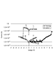
- FIG. 3 is an experimental result showing the current-voltage characteristics of the variable resistance element according to the comparative example, and has the same configuration as the variable resistance element 1 according to the embodiment except that the upper electrode layer is composed of Pt.
- Pt is a typical example of a metal material having a work function larger than that of an oxide semiconductor layer having N-type conductivity, and forms a Schottky junction at the interface with the oxide semiconductor layer.
- the resistance change element according to the comparative example requires a forming voltage of about 9V as shown in FIG. 3, and requires a switching voltage of about 3V.
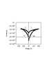
- the resistance change element 1 according to the present embodiment does not require the initialization operation as shown in FIG. 2, and the switching voltage can be suppressed to as low as about 0.8V.
- the resistance change element 1 according to the present embodiment can suppress the operating current (readout current) in the low resistance state to be lower than that of the resistance change element according to the comparative example.
- the power consumption of the element can be significantly reduced.
- the resistance change element 1 of the present embodiment since the forming is not required, generation of a non-uniform filament in the oxide semiconductor layer 4 can be suppressed. It is possible to stably manufacture a variable resistance element having specific characteristics. Furthermore, since the filament dependency of the operating current can be reduced, the driving current of the element can be controlled by the element size.
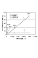
- FIG. 4 shows an example of the electrode area dependency of the read current.
- the horizontal axis indicates the area of the upper electrode, and the vertical axis indicates the current value of 0.5 V applied character.
- “a” indicates the current characteristic of the variable resistance element according to the comparative example
- “b” indicates the current characteristic of the variable resistance element according to the present embodiment.
- the resistance change element according to the comparative example has a substantially constant read current regardless of the electrode area
- the resistance change element according to the present embodiment has a read current proportional to the electrode area. It turns out that it is obtained. This shows that the drive current of the element can be controlled by the element size.
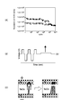
- FIG. 5 and 6 show experimental results for evaluating the stability of the switching operation of the variable resistance element according to the comparative example.
- FIG. 5 shows the read voltage when the read voltage is a positive voltage (+0.5 V), and FIG. Indicates a negative voltage ( ⁇ 0.5 V).
- A shows the repetitive switching characteristics
- B shows the applied pulse waveform
- C shows the switching model of the element.
- the on / off ratio gradually changes as the switching cycle increases as shown in FIG. 5A, whereas when the read voltage is a negative voltage, As shown in FIG. 6A, it was confirmed that a constant on / off ratio was maintained near 10 9 times and stable switching operation was exhibited. This is because when the read voltage is a positive voltage, the conduction path (filament) formed in the oxide semiconductor layer gradually increases as shown in FIG. 5C, whereas the read voltage is a negative voltage. In this case, it is assumed that the thickness of the conduction path does not change as shown in FIG.
- the first metal oxide layer 41 is composed of a stoichiometric composition material
- the second metal oxide layer 42 is composed of an oxygen deficient material.
- the oxide layer 41 may be composed of an oxygen-deficient material
- the second metal oxide layer may be composed of a stoichiometric composition material.
- the 1st metal oxide layer 41 and the 2nd metal oxide layer 42 were comprised with the same kind of metal oxide, it is not restricted to this, The same conductivity type (N type or P type) ),
- the combination of materials is arbitrary.
- different materials may be combined for the lower electrode layer 3 and the upper electrode layer 5 as long as they conform to the conductivity type of the oxide semiconductor.
Landscapes
- Engineering & Computer Science (AREA)
- Manufacturing & Machinery (AREA)
- Chemical & Material Sciences (AREA)
- Materials Engineering (AREA)
- Computer Hardware Design (AREA)
- Semiconductor Memories (AREA)
Abstract
Description
上記酸化物半導体は、第1の金属酸化物層と、第2の金属酸化物層とを有する。上記第1の金属酸化物層は、上記第1の電極と上記第2の電極との間に形成され、上記第1の電極とオーミック接合される。上記第2の金属酸化物層は、上記第1の金属酸化物層と上記第2の電極との間に形成され、上記第2の電極とオーミック接合される。
上記第1の電極の上に、第1の金属酸化物層が形成される。上記第1の金属酸化物層は、第1の抵抗率を有し、N型酸化物半導体で構成される。
上記第1の金属酸化物層の上に、第2の金属酸化物層が形成される。上記第2の金属酸化物層は、上記第1の抵抗率と異なる第2の抵抗率を有し、N型酸化物半導体で構成される。
上記第2の金属酸化物層の上に、Ti,V,Cr,Zr,Nb,Mo,Hf,Ta,Wのいずれかの金属、あるいはその化合物で構成された第2の電極が形成される。
上記第1の電極の上に、第1の金属酸化物層が形成される。上記第1の金属酸化物層は、第1の抵抗率を有し、P型酸化物半導体で構成される。
上記第1の金属酸化物層の上に、第2の金属酸化物層が形成される。上記第2の金属酸化物層は、前記第1の抵抗率と異なる第2の抵抗率を有し、P型酸化物半導体で構成される。
上記第2の金属酸化物層の上に、Fe,Co,Ni,Cu,Ru,Rh,Pd,Ag,Os,Ir,Pt,Auのいずれかの金属、あるいはその化合物で構成された第2の電極が形成される。
上記酸化物半導体は、第1の金属酸化物層と、第2の金属酸化物層とを有する。上記第1の金属酸化物層は、上記第1の電極と上記第2の電極との間に形成され、上記第1の電極とオーミック接合される。上記第2の金属酸化物層は、上記第1の金属酸化物層と上記第2の電極との間に形成され、上記第2の電極とオーミック接合される。
上記第1の電極の上に、第1の金属酸化物層が形成される。上記第1の金属酸化物層は、第1の抵抗率を有し、N型酸化物半導体で構成される。
上記第1の金属酸化物層の上に、第2の金属酸化物層が形成される。上記第2の金属酸化物層は、上記第1の抵抗率と異なる第2の抵抗率を有し、N型酸化物半導体で構成される。
上記第2の金属酸化物層の上に、Ti,V,Cr,Zr,Nb,Mo,Hf,Ta,Wのいずれかの金属、あるいはその化合物で構成された第2の電極が形成される。
上記第1の電極の上に、第1の金属酸化物層が形成される。上記第1の金属酸化物層は、第1の抵抗率を有し、P型酸化物半導体で構成される。
上記第1の金属酸化物層の上に、第2の金属酸化物層が形成される。上記第2の金属酸化物層は、前記第1の抵抗率と異なる第2の抵抗率を有し、P型酸化物半導体で構成される。
上記第2の金属酸化物層の上に、Fe,Co,Ni,Cu,Ru,Rh,Pd,Ag,Os,Ir,Pt,Auのいずれかの金属、あるいはその化合物で構成された第2の電極が形成される。
(2)Pt,Ir,Ru,Pd,TiN,TiAlN,TaNなどの酸化耐性がある電極上にALD法、CVD法、酸化ガスによる反応性スパッタ法などにより、金属酸化物を多積させる。
(3)IrOx,RuOx,SrRuO3,LaNiO3,ITOなどの酸化物電気伝導体上にALD法、CVD法、酸化ガスによる反応性スパッタ法などにより、金属酸化物を堆積させる。
(4)TaC,WSi,WGeなど、Si,C,Geなど還元力の強い元素が含まれる電気伝導体上にALD法、CVD法、酸化ガスによる反応性スパッタ法などにより、金属酸化物を耐性させる。
(5)下部電極層3上に堆積された金属酸化物の下部電極界面近傍に、ドナー元素またはアクセプタ元素をイオン注入、プラズマドープしたり、上記元素を成膜ガスやターゲットに混入する。
(6)電位障壁を形成しない金属材料と酸化物材料を組み合わせる。
2…基板
3…下部電極層
4…酸化物半導体層
5…上部電極層
41…第1の金属酸化物層
42…第2の金属酸化物層
Claims (5)
- 第1の電極と、
第2の電極と、
前記第1の電極と前記第2の電極との間に形成され、前記第1の電極とオーミック接合される第1の金属酸化物層と、前記第1の金属酸化物と前記第2の電極との間に形成され、前記第2の電極とオーミック接合される第2の金属酸化物層とを有する酸化物半導体と
を具備する抵抗変化素子。 - 請求項1に記載の抵抗変化素子であって、
前記第1の金属酸化物層及び前記第2の金属酸化物層は、N型酸化物半導体であり、
前記第1の電極及び前記第2の電極は、Ti,V,Cr,Zr,Nb,Mo,Hf,Ta,Wのいずれかの金属あるいはその化合物である
抵抗変化素子。 - 請求項1に記載の抵抗変化素子であって、
前記第1の金属酸化物層及び前記第2の金属酸化物層は、P型酸化物半導体であり、
前記第1の電極及び前記第2の電極は、Fe,Co,Ni,Cu,Ru,Rh,Pd,Ag,Os,Ir,Pt,Auのいずれかの金属あるいはその化合物である
抵抗変化素子。 - 基板上に、Ti,V,Cr,Zr,Nb,Mo,Hf,Ta,Wのいずれかの金属あるいはその化合物で構成された第1の電極を形成し、
前記第1の電極の上に、第1の抵抗率を有し、N型酸化物半導体で構成された第1の金属酸化物層を形成し、
前記第1の金属酸化物層の上に、前記第1の抵抗率と異なる第2の抵抗率を有し、N型酸化物半導体で構成された第2の金属酸化物層を形成し、
前記第2の金属酸化物層の上に、Ti,V,Cr,Zr,Nb,Mo,Hf,Ta,Wのいずれかの金属あるいはその化合物で構成された第2の電極を形成する
抵抗変化素子の製造方法。 - 基板上に、Fe,Co,Ni,Cu,Ru,Rh,Pd,Ag,Os,Ir,Pt,Auのいずれかの金属あるいはその化合物で構成された第1の電極を形成し、
前記第1の電極の上に、第1の抵抗率を有し、P型酸化物半導体で構成された第1の金属酸化物層を形成し、
前記第1の金属酸化物層の上に、前記第1の抵抗率と異なる第2の抵抗率を有し、P型酸化物半導体で構成された第2の金属酸化物層を形成し、
前記第2の金属酸化物層の上に、Fe,Co,Ni,Cu,Ru,Rh,Pd,Ag,Os,Ir,Pt,Auのいずれかの金属あるいはその化合物で構成された第2の電極を形成する
抵抗変化素子の製造方法。
Priority Applications (4)
| Application Number | Priority Date | Filing Date | Title |
|---|---|---|---|
| JP2013519389A JP5648126B2 (ja) | 2011-06-10 | 2012-06-07 | 抵抗変化素子及びその製造方法 |
| CN201280028327.9A CN103597597B (zh) | 2011-06-10 | 2012-06-07 | 可变电阻元件及其制造方法 |
| KR1020137032350A KR101528094B1 (ko) | 2011-06-10 | 2012-06-07 | 저항 변화 소자 및 그 제조 방법 |
| US14/125,254 US9281477B2 (en) | 2011-06-10 | 2012-06-17 | Resistance change element and method for producing the same |
Applications Claiming Priority (2)
| Application Number | Priority Date | Filing Date | Title |
|---|---|---|---|
| JP2011130011 | 2011-06-10 | ||
| JP2011-130011 | 2011-06-10 |
Publications (1)
| Publication Number | Publication Date |
|---|---|
| WO2012169195A1 true WO2012169195A1 (ja) | 2012-12-13 |
Family
ID=47295778
Family Applications (1)
| Application Number | Title | Priority Date | Filing Date |
|---|---|---|---|
| PCT/JP2012/003728 Ceased WO2012169195A1 (ja) | 2011-06-10 | 2012-06-07 | 抵抗変化素子及びその製造方法 |
Country Status (6)
| Country | Link |
|---|---|
| US (1) | US9281477B2 (ja) |
| JP (1) | JP5648126B2 (ja) |
| KR (1) | KR101528094B1 (ja) |
| CN (1) | CN103597597B (ja) |
| TW (1) | TWI562386B (ja) |
| WO (1) | WO2012169195A1 (ja) |
Cited By (3)
| Publication number | Priority date | Publication date | Assignee | Title |
|---|---|---|---|---|
| WO2014038152A1 (ja) * | 2012-09-05 | 2014-03-13 | 株式会社アルバック | 抵抗変化素子及びその製造方法 |
| JP2014116605A (ja) * | 2012-12-10 | 2014-06-26 | Huabang Electronic Co Ltd | 自己整流型rramセル構造およびそのクロスバーアレイ構造 |
| JP2014146633A (ja) * | 2013-01-28 | 2014-08-14 | National Institute For Materials Science | 多機能電気伝導素子 |
Families Citing this family (7)
| Publication number | Priority date | Publication date | Assignee | Title |
|---|---|---|---|---|
| TWI556245B (zh) * | 2015-02-16 | 2016-11-01 | 國立中山大學 | 電阻式記憶體 |
| US9741930B2 (en) | 2015-03-27 | 2017-08-22 | Intel Corporation | Materials and components in phase change memory devices |
| JP2018006696A (ja) * | 2016-07-08 | 2018-01-11 | 東芝メモリ株式会社 | 記憶装置 |
| CN109643660B (zh) * | 2016-08-31 | 2024-03-05 | 株式会社Flosfia | p-型氧化物半导体及其制造方法 |
| US10164169B2 (en) * | 2016-09-30 | 2018-12-25 | Taiwan Semiconductor Manufacturing Co., Ltd. | Memory device having a single bottom electrode layer |
| US12046658B2 (en) * | 2019-07-11 | 2024-07-23 | Micron Technology, Inc. | Electrode formation |
| CN111341909A (zh) * | 2020-02-07 | 2020-06-26 | 中国科学院微电子研究所 | 一种存储器件及其制作方法、存储器及电子设备 |
Citations (3)
| Publication number | Priority date | Publication date | Assignee | Title |
|---|---|---|---|---|
| WO2006075574A1 (ja) * | 2005-01-14 | 2006-07-20 | Matsushita Electric Industrial Co., Ltd. | 抵抗変化素子とその製造方法 |
| WO2007138646A1 (ja) * | 2006-05-25 | 2007-12-06 | Hitachi, Ltd. | 不揮発性メモリ素子およびその製造方法ならびに不揮発性メモリ素子を用いた半導体装置 |
| WO2008149484A1 (ja) * | 2007-06-05 | 2008-12-11 | Panasonic Corporation | 不揮発性記憶素子およびその製造方法、並びにその不揮発性記憶素子を用いた不揮発性半導体装置 |
Family Cites Families (7)
| Publication number | Priority date | Publication date | Assignee | Title |
|---|---|---|---|---|
| KR101275800B1 (ko) * | 2006-04-28 | 2013-06-18 | 삼성전자주식회사 | 가변 저항 물질을 포함하는 비휘발성 메모리 소자 |
| JP5152173B2 (ja) | 2007-03-01 | 2013-02-27 | 富士通株式会社 | 半導体装置及びその製造方法 |
| US8173989B2 (en) * | 2007-05-30 | 2012-05-08 | Samsung Electronics Co., Ltd. | Resistive random access memory device and methods of manufacturing and operating the same |
| WO2009136493A1 (ja) * | 2008-05-08 | 2009-11-12 | パナソニック株式会社 | 不揮発性記憶素子、及び、不揮発性記憶素子又は不揮発性記憶装置の製造方法 |
| JP4937413B2 (ja) * | 2008-12-10 | 2012-05-23 | パナソニック株式会社 | 抵抗変化素子およびそれを用いた不揮発性半導体記憶装置 |
| WO2010073897A1 (ja) | 2008-12-26 | 2010-07-01 | 日本電気株式会社 | 抵抗変化素子 |
| JP4792097B2 (ja) * | 2009-03-25 | 2011-10-12 | 株式会社東芝 | 不揮発性記憶装置及びその製造方法 |
-
2012
- 2012-06-07 KR KR1020137032350A patent/KR101528094B1/ko active Active
- 2012-06-07 JP JP2013519389A patent/JP5648126B2/ja active Active
- 2012-06-07 CN CN201280028327.9A patent/CN103597597B/zh active Active
- 2012-06-07 WO PCT/JP2012/003728 patent/WO2012169195A1/ja not_active Ceased
- 2012-06-08 TW TW101120744A patent/TWI562386B/zh active
- 2012-06-17 US US14/125,254 patent/US9281477B2/en active Active
Patent Citations (3)
| Publication number | Priority date | Publication date | Assignee | Title |
|---|---|---|---|---|
| WO2006075574A1 (ja) * | 2005-01-14 | 2006-07-20 | Matsushita Electric Industrial Co., Ltd. | 抵抗変化素子とその製造方法 |
| WO2007138646A1 (ja) * | 2006-05-25 | 2007-12-06 | Hitachi, Ltd. | 不揮発性メモリ素子およびその製造方法ならびに不揮発性メモリ素子を用いた半導体装置 |
| WO2008149484A1 (ja) * | 2007-06-05 | 2008-12-11 | Panasonic Corporation | 不揮発性記憶素子およびその製造方法、並びにその不揮発性記憶素子を用いた不揮発性半導体装置 |
Cited By (5)
| Publication number | Priority date | Publication date | Assignee | Title |
|---|---|---|---|---|
| WO2014038152A1 (ja) * | 2012-09-05 | 2014-03-13 | 株式会社アルバック | 抵抗変化素子及びその製造方法 |
| JP5696260B2 (ja) * | 2012-09-05 | 2015-04-08 | 株式会社アルバック | 抵抗変化素子及びその製造方法 |
| US9343207B2 (en) | 2012-09-05 | 2016-05-17 | Ulvac, Inc. | Resistance change device, and method for producing same |
| JP2014116605A (ja) * | 2012-12-10 | 2014-06-26 | Huabang Electronic Co Ltd | 自己整流型rramセル構造およびそのクロスバーアレイ構造 |
| JP2014146633A (ja) * | 2013-01-28 | 2014-08-14 | National Institute For Materials Science | 多機能電気伝導素子 |
Also Published As
| Publication number | Publication date |
|---|---|
| CN103597597B (zh) | 2016-09-14 |
| KR101528094B1 (ko) | 2015-06-10 |
| CN103597597A (zh) | 2014-02-19 |
| JPWO2012169195A1 (ja) | 2015-02-23 |
| US9281477B2 (en) | 2016-03-08 |
| TW201310659A (zh) | 2013-03-01 |
| US20140166966A1 (en) | 2014-06-19 |
| JP5648126B2 (ja) | 2015-01-07 |
| KR20140014274A (ko) | 2014-02-05 |
| TWI562386B (en) | 2016-12-11 |
Similar Documents
| Publication | Publication Date | Title |
|---|---|---|
| JP5648126B2 (ja) | 抵抗変化素子及びその製造方法 | |
| JP5339716B2 (ja) | 抵抗メモリ素子及びその製造方法 | |
| JP5154138B2 (ja) | n+界面層を備えた可変抵抗ランダムアクセスメモリ素子 | |
| US8125021B2 (en) | Non-volatile memory devices including variable resistance material | |
| KR101783086B1 (ko) | 저항-전환층들을 가진 메모리 셀의 구성 | |
| US10217797B2 (en) | Switching device, and resistive random access memory including the same as a selection device | |
| US20090302315A1 (en) | Resistive random access memory | |
| US8599603B2 (en) | Resistive-switching nonvolatile memory elements | |
| US20140124728A1 (en) | Resistive memory device, resistive memory array, and method of manufacturing resistive memory device | |
| JP2008016854A (ja) | 可変抵抗物質を含む不揮発性メモリ素子 | |
| US20080308783A1 (en) | Memory devices and methods of manufacturing the same | |
| JP2008135752A (ja) | ドーパントを含む抵抗性メモリ素子及びその製造方法 | |
| KR20130126325A (ko) | 가변 저항 메모리 장치 및 그 제조 방법 | |
| JP2008022007A (ja) | 可変抵抗物質を含む不揮発性メモリ素子及びその製造方法 | |
| JPWO2009096363A1 (ja) | 抵抗変化型不揮発性記憶装置とその製造方法 | |
| JP2017055082A (ja) | 不揮発性記憶装置の製造方法 | |
| KR20170089726A (ko) | 스위칭 소자, 이의 제조 방법, 스위칭 소자를 선택 소자로서 포함하는 저항 변화 메모리 장치 | |
| WO2010073897A1 (ja) | 抵抗変化素子 | |
| JP2007335869A (ja) | Cu2Oを含む不揮発性可変抵抗メモリ素子 | |
| KR101285903B1 (ko) | 자체 선택 특성을 가지는 3층 저항변화 메모리 및 이의 제조방법 | |
| JP2013207131A (ja) | 抵抗変化素子及びその製造方法 | |
| KR20100133761A (ko) | 저항 변화 메모리 소자 및 그 제조방법 | |
| KR20150128930A (ko) | 도펀트 보상형 스위칭을 갖는 멤리스터 | |
| JP2011091329A (ja) | 抵抗変化型メモリ素子、及び、抵抗変化型不揮発性メモリ、並びに、抵抗変化型メモリ素子制御方法 | |
| KR20220015823A (ko) | 저항 변화 소자 및 이의 제조방법 |
Legal Events
| Date | Code | Title | Description |
|---|---|---|---|
| 121 | Ep: the epo has been informed by wipo that ep was designated in this application |
Ref document number: 12797334 Country of ref document: EP Kind code of ref document: A1 |
|
| ENP | Entry into the national phase |
Ref document number: 2013519389 Country of ref document: JP Kind code of ref document: A |
|
| ENP | Entry into the national phase |
Ref document number: 20137032350 Country of ref document: KR Kind code of ref document: A |
|
| NENP | Non-entry into the national phase |
Ref country code: DE |
|
| WWE | Wipo information: entry into national phase |
Ref document number: 14125254 Country of ref document: US |
|
| 122 | Ep: pct application non-entry in european phase |
Ref document number: 12797334 Country of ref document: EP Kind code of ref document: A1 |