WO2012165530A1 - 多層基板の製造方法および多層基板 - Google Patents
多層基板の製造方法および多層基板 Download PDFInfo
- Publication number
- WO2012165530A1 WO2012165530A1 PCT/JP2012/064044 JP2012064044W WO2012165530A1 WO 2012165530 A1 WO2012165530 A1 WO 2012165530A1 JP 2012064044 W JP2012064044 W JP 2012064044W WO 2012165530 A1 WO2012165530 A1 WO 2012165530A1
- Authority
- WO
- WIPO (PCT)
- Prior art keywords
- substrate
- core
- resin layer
- main surfaces
- resin
- Prior art date
- Legal status (The legal status is an assumption and is not a legal conclusion. Google has not performed a legal analysis and makes no representation as to the accuracy of the status listed.)
- Ceased
Links
Images





Classifications
-
- H—ELECTRICITY
- H05—ELECTRIC TECHNIQUES NOT OTHERWISE PROVIDED FOR
- H05K—PRINTED CIRCUITS; CASINGS OR CONSTRUCTIONAL DETAILS OF ELECTRIC APPARATUS; MANUFACTURE OF ASSEMBLAGES OF ELECTRICAL COMPONENTS
- H05K1/00—Printed circuits
- H05K1/18—Printed circuits structurally associated with non-printed electric components
- H05K1/181—Printed circuits structurally associated with non-printed electric components associated with surface mounted components
-
- H—ELECTRICITY
- H10—SEMICONDUCTOR DEVICES; ELECTRIC SOLID-STATE DEVICES NOT OTHERWISE PROVIDED FOR
- H10W—GENERIC PACKAGES, INTERCONNECTIONS, CONNECTORS OR OTHER CONSTRUCTIONAL DETAILS OF DEVICES COVERED BY CLASS H10
- H10W70/00—Package substrates; Interposers; Redistribution layers [RDL]
- H10W70/60—Insulating or insulated package substrates; Interposers; Redistribution layers
- H10W70/67—Insulating or insulated package substrates; Interposers; Redistribution layers characterised by their insulating layers or insulating parts
- H10W70/68—Shapes or dispositions thereof
-
- H—ELECTRICITY
- H05—ELECTRIC TECHNIQUES NOT OTHERWISE PROVIDED FOR
- H05K—PRINTED CIRCUITS; CASINGS OR CONSTRUCTIONAL DETAILS OF ELECTRIC APPARATUS; MANUFACTURE OF ASSEMBLAGES OF ELECTRICAL COMPONENTS
- H05K3/00—Apparatus or processes for manufacturing printed circuits
- H05K3/22—Secondary treatment of printed circuits
- H05K3/28—Applying non-metallic protective coatings
- H05K3/284—Applying non-metallic protective coatings for encapsulating mounted components
-
- H—ELECTRICITY
- H05—ELECTRIC TECHNIQUES NOT OTHERWISE PROVIDED FOR
- H05K—PRINTED CIRCUITS; CASINGS OR CONSTRUCTIONAL DETAILS OF ELECTRIC APPARATUS; MANUFACTURE OF ASSEMBLAGES OF ELECTRICAL COMPONENTS
- H05K3/00—Apparatus or processes for manufacturing printed circuits
- H05K3/30—Assembling printed circuits with electric components, e.g. with resistors
- H05K3/303—Assembling printed circuits with electric components, e.g. with resistors with surface mounted components
-
- H—ELECTRICITY
- H10—SEMICONDUCTOR DEVICES; ELECTRIC SOLID-STATE DEVICES NOT OTHERWISE PROVIDED FOR
- H10W—GENERIC PACKAGES, INTERCONNECTIONS, CONNECTORS OR OTHER CONSTRUCTIONAL DETAILS OF DEVICES COVERED BY CLASS H10
- H10W42/00—Arrangements for protection of devices
- H10W42/20—Arrangements for protection of devices protecting against electromagnetic or particle radiation, e.g. light, X-rays, gamma-rays or electrons
- H10W42/261—Arrangements for protection of devices protecting against electromagnetic or particle radiation, e.g. light, X-rays, gamma-rays or electrons characterised by their shapes or dispositions
- H10W42/276—Arrangements for protection of devices protecting against electromagnetic or particle radiation, e.g. light, X-rays, gamma-rays or electrons characterised by their shapes or dispositions the arrangements being on an external surface of the package, e.g. on the outer surface of an encapsulation
-
- H—ELECTRICITY
- H10—SEMICONDUCTOR DEVICES; ELECTRIC SOLID-STATE DEVICES NOT OTHERWISE PROVIDED FOR
- H10W—GENERIC PACKAGES, INTERCONNECTIONS, CONNECTORS OR OTHER CONSTRUCTIONAL DETAILS OF DEVICES COVERED BY CLASS H10
- H10W74/00—Encapsulations, e.g. protective coatings
- H10W74/01—Manufacture or treatment
- H10W74/014—Manufacture or treatment using batch processing
-
- H—ELECTRICITY
- H10—SEMICONDUCTOR DEVICES; ELECTRIC SOLID-STATE DEVICES NOT OTHERWISE PROVIDED FOR
- H10W—GENERIC PACKAGES, INTERCONNECTIONS, CONNECTORS OR OTHER CONSTRUCTIONAL DETAILS OF DEVICES COVERED BY CLASS H10
- H10W74/00—Encapsulations, e.g. protective coatings
- H10W74/10—Encapsulations, e.g. protective coatings characterised by their shape or disposition
- H10W74/111—Encapsulations, e.g. protective coatings characterised by their shape or disposition the semiconductor body being completely enclosed
-
- H—ELECTRICITY
- H10—SEMICONDUCTOR DEVICES; ELECTRIC SOLID-STATE DEVICES NOT OTHERWISE PROVIDED FOR
- H10W—GENERIC PACKAGES, INTERCONNECTIONS, CONNECTORS OR OTHER CONSTRUCTIONAL DETAILS OF DEVICES COVERED BY CLASS H10
- H10W90/00—Package configurations
- H10W90/701—Package configurations characterised by the relative positions of pads or connectors relative to package parts
-
- H—ELECTRICITY
- H05—ELECTRIC TECHNIQUES NOT OTHERWISE PROVIDED FOR
- H05K—PRINTED CIRCUITS; CASINGS OR CONSTRUCTIONAL DETAILS OF ELECTRIC APPARATUS; MANUFACTURE OF ASSEMBLAGES OF ELECTRICAL COMPONENTS
- H05K1/00—Printed circuits
- H05K1/02—Details
- H05K1/0271—Arrangements for reducing stress or warp in rigid printed circuit boards, e.g. caused by loads, vibrations or differences in thermal expansion
-
- H—ELECTRICITY
- H05—ELECTRIC TECHNIQUES NOT OTHERWISE PROVIDED FOR
- H05K—PRINTED CIRCUITS; CASINGS OR CONSTRUCTIONAL DETAILS OF ELECTRIC APPARATUS; MANUFACTURE OF ASSEMBLAGES OF ELECTRICAL COMPONENTS
- H05K2201/00—Indexing scheme relating to printed circuits covered by H05K1/00
- H05K2201/09—Shape and layout
- H05K2201/09009—Substrate related
- H05K2201/09063—Holes or slots in insulating substrate not used for electrical connections
-
- H—ELECTRICITY
- H05—ELECTRIC TECHNIQUES NOT OTHERWISE PROVIDED FOR
- H05K—PRINTED CIRCUITS; CASINGS OR CONSTRUCTIONAL DETAILS OF ELECTRIC APPARATUS; MANUFACTURE OF ASSEMBLAGES OF ELECTRICAL COMPONENTS
- H05K2201/00—Indexing scheme relating to printed circuits covered by H05K1/00
- H05K2201/10—Details of components or other objects attached to or integrated in a printed circuit board
- H05K2201/10227—Other objects, e.g. metallic pieces
- H05K2201/1031—Surface mounted metallic connector elements
- H05K2201/10318—Surface mounted metallic pins
-
- H—ELECTRICITY
- H05—ELECTRIC TECHNIQUES NOT OTHERWISE PROVIDED FOR
- H05K—PRINTED CIRCUITS; CASINGS OR CONSTRUCTIONAL DETAILS OF ELECTRIC APPARATUS; MANUFACTURE OF ASSEMBLAGES OF ELECTRICAL COMPONENTS
- H05K2203/00—Indexing scheme relating to apparatus or processes for manufacturing printed circuits covered by H05K3/00
- H05K2203/13—Moulding and encapsulation; Deposition techniques; Protective layers
- H05K2203/1305—Moulding and encapsulation
- H05K2203/1316—Moulded encapsulation of mounted components
-
- H—ELECTRICITY
- H05—ELECTRIC TECHNIQUES NOT OTHERWISE PROVIDED FOR
- H05K—PRINTED CIRCUITS; CASINGS OR CONSTRUCTIONAL DETAILS OF ELECTRIC APPARATUS; MANUFACTURE OF ASSEMBLAGES OF ELECTRICAL COMPONENTS
- H05K2203/00—Indexing scheme relating to apparatus or processes for manufacturing printed circuits covered by H05K3/00
- H05K2203/15—Position of the PCB during processing
- H05K2203/1572—Processing both sides of a PCB by the same process; Providing a similar arrangement of components on both sides; Making interlayer connections from two sides
-
- H—ELECTRICITY
- H05—ELECTRIC TECHNIQUES NOT OTHERWISE PROVIDED FOR
- H05K—PRINTED CIRCUITS; CASINGS OR CONSTRUCTIONAL DETAILS OF ELECTRIC APPARATUS; MANUFACTURE OF ASSEMBLAGES OF ELECTRICAL COMPONENTS
- H05K3/00—Apparatus or processes for manufacturing printed circuits
- H05K3/0097—Processing two or more printed circuits simultaneously, e.g. made from a common substrate, or temporarily stacked circuit boards
-
- H—ELECTRICITY
- H10—SEMICONDUCTOR DEVICES; ELECTRIC SOLID-STATE DEVICES NOT OTHERWISE PROVIDED FOR
- H10W—GENERIC PACKAGES, INTERCONNECTIONS, CONNECTORS OR OTHER CONSTRUCTIONAL DETAILS OF DEVICES COVERED BY CLASS H10
- H10W42/00—Arrangements for protection of devices
- H10W42/20—Arrangements for protection of devices protecting against electromagnetic or particle radiation, e.g. light, X-rays, gamma-rays or electrons
-
- H—ELECTRICITY
- H10—SEMICONDUCTOR DEVICES; ELECTRIC SOLID-STATE DEVICES NOT OTHERWISE PROVIDED FOR
- H10W—GENERIC PACKAGES, INTERCONNECTIONS, CONNECTORS OR OTHER CONSTRUCTIONAL DETAILS OF DEVICES COVERED BY CLASS H10
- H10W70/00—Package substrates; Interposers; Redistribution layers [RDL]
- H10W70/60—Insulating or insulated package substrates; Interposers; Redistribution layers
- H10W70/67—Insulating or insulated package substrates; Interposers; Redistribution layers characterised by their insulating layers or insulating parts
- H10W70/68—Shapes or dispositions thereof
- H10W70/685—Shapes or dispositions thereof comprising multiple insulating layers
-
- H—ELECTRICITY
- H10—SEMICONDUCTOR DEVICES; ELECTRIC SOLID-STATE DEVICES NOT OTHERWISE PROVIDED FOR
- H10W—GENERIC PACKAGES, INTERCONNECTIONS, CONNECTORS OR OTHER CONSTRUCTIONAL DETAILS OF DEVICES COVERED BY CLASS H10
- H10W72/00—Interconnections or connectors in packages
- H10W72/01—Manufacture or treatment
- H10W72/0198—Manufacture or treatment batch processes
-
- H—ELECTRICITY
- H10—SEMICONDUCTOR DEVICES; ELECTRIC SOLID-STATE DEVICES NOT OTHERWISE PROVIDED FOR
- H10W—GENERIC PACKAGES, INTERCONNECTIONS, CONNECTORS OR OTHER CONSTRUCTIONAL DETAILS OF DEVICES COVERED BY CLASS H10
- H10W74/00—Encapsulations, e.g. protective coatings
-
- H—ELECTRICITY
- H10—SEMICONDUCTOR DEVICES; ELECTRIC SOLID-STATE DEVICES NOT OTHERWISE PROVIDED FOR
- H10W—GENERIC PACKAGES, INTERCONNECTIONS, CONNECTORS OR OTHER CONSTRUCTIONAL DETAILS OF DEVICES COVERED BY CLASS H10
- H10W74/00—Encapsulations, e.g. protective coatings
- H10W74/40—Encapsulations, e.g. protective coatings characterised by their materials
- H10W74/47—Encapsulations, e.g. protective coatings characterised by their materials comprising organic materials, e.g. plastics or resins
- H10W74/473—Encapsulations, e.g. protective coatings characterised by their materials comprising organic materials, e.g. plastics or resins containing a filler
-
- H—ELECTRICITY
- H10—SEMICONDUCTOR DEVICES; ELECTRIC SOLID-STATE DEVICES NOT OTHERWISE PROVIDED FOR
- H10W—GENERIC PACKAGES, INTERCONNECTIONS, CONNECTORS OR OTHER CONSTRUCTIONAL DETAILS OF DEVICES COVERED BY CLASS H10
- H10W90/00—Package configurations
- H10W90/701—Package configurations characterised by the relative positions of pads or connectors relative to package parts
- H10W90/721—Package configurations characterised by the relative positions of pads or connectors relative to package parts of bump connectors
- H10W90/724—Package configurations characterised by the relative positions of pads or connectors relative to package parts of bump connectors between a chip and a stacked insulating package substrate, interposer or RDL
-
- Y—GENERAL TAGGING OF NEW TECHNOLOGICAL DEVELOPMENTS; GENERAL TAGGING OF CROSS-SECTIONAL TECHNOLOGIES SPANNING OVER SEVERAL SECTIONS OF THE IPC; TECHNICAL SUBJECTS COVERED BY FORMER USPC CROSS-REFERENCE ART COLLECTIONS [XRACs] AND DIGESTS
- Y10—TECHNICAL SUBJECTS COVERED BY FORMER USPC
- Y10T—TECHNICAL SUBJECTS COVERED BY FORMER US CLASSIFICATION
- Y10T29/00—Metal working
- Y10T29/49—Method of mechanical manufacture
- Y10T29/49002—Electrical device making
- Y10T29/49117—Conductor or circuit manufacturing
- Y10T29/49124—On flat or curved insulated base, e.g., printed circuit, etc.
- Y10T29/4913—Assembling to base an electrical component, e.g., capacitor, etc.
Definitions
- the present invention relates to a multilayer substrate and a method for manufacturing the multilayer substrate, and more particularly, to a multilayer substrate having a structure in which both main surfaces of a core substrate on which surface-mounted components are mounted are sealed with a sealing resin layer and the manufacture thereof. Regarding the method.
- a multilayer substrate having a configuration as shown in FIG. 14 has been proposed as one of the multilayer substrates.
- this multilayer substrate has a core substrate (ceramic multilayer substrate) 110 composed of a plurality of laminated ceramic layers, and an active chip component 140 such as a semiconductor device is arranged on one main surface.
- a passive chip component 150 such as a capacitor is disposed on the other main surface.
- resin layers 120 and 130 for sealing are formed on both main surfaces of the core substrate (ceramic multilayer substrate) 110, and surface electrodes 121 and via conductors 122 are formed on the resin layer 130 on the lower surface side. ing.
- the resin is cured when the resin layers 120 and 130 are formed.
- warpage occurs in the core substrate 110 due to the difference in expansion and contraction rate between the core substrate 110 and the resin layers 120 and 130, and the mounting reliability when the multilayer substrate is mounted on a module substrate or the like is reduced.
- the conductor disposed on the multilayer substrate may be disconnected.
- peeling may occur between the core substrate 110 and the resin layers 120 and 130 due to thermal stress between the core substrate 110 and the resin layers 120 and 130.
- the present invention solves the above problems, and in manufacturing a multilayer substrate having a structure in which both main surfaces of a core substrate are sealed with a sealing resin layer, warping occurs in the step of curing the resin layer.
- An object of the present invention is to provide a method for manufacturing a multilayer substrate that can suppress the occurrence and reliably manufacture a multilayer substrate without warping and having high reliability.
- a method for producing a multilayer substrate of the present invention includes: A method for producing a multilayer substrate comprising a sealing resin layer disposed on both main surfaces of a core substrate, (a) A surface mount component to be sealed by the sealing layer is mounted on both main surface sides of a core parent substrate including a plurality of core individual substrates and having through holes penetrating each core individual substrate.
- Forming a mounted core parent substrate (b) so that the resin layers on both main surfaces of each core substrate obtained by dividing the core parent substrate in the following steps are combined and integrated with each other in a predetermined region, A resin layer forming step of forming a semi-cured resin layer on both main surfaces of the core mother substrate and bonding the resin layers on both main surfaces to each other through the through holes; (c) a resin layer curing step of fully curing the semi-cured resin layer formed on the core parent substrate; and (d) a splitting step in which the core parent substrate including the resin layer that has been hardened in the resin layer curing step is divided at a predetermined position into individual core substrates.
- the term “through hole penetrating each core substrate” refers to a case where a complete through hole penetrates the core substrate and a case where a part of the through hole penetrates the core substrate. (That is, when one through-hole penetrates the core unit substrate over a plurality of core unit substrates).
- the resin layer on both main surfaces provided on the core substrate is coupled to and integrated with each other in a predetermined region of the peripheral portion. It is preferable to form a through hole that cuts out a part of the outer peripheral edge of each core substrate included.
- the resin layers on both main surfaces of the core substrate are combined and integrated with each other at the peripheral portion, so that a highly reliable multilayer substrate without warping can be obtained.
- the central region of the core substrate is not used as a region for bonding the resin layer, the central region of the core substrate can be effectively used as a mounting region for surface-mounted components.
- each of the resin layers on both main surfaces provided on the core substrate is coupled to and integrated with each other in a region penetrating the core substrate, and each included in the core parent substrate as the through hole. It is preferable to form a through-hole penetrating the core substrate region.
- the semi-cured state is used as a dividing groove for dividing the core parent substrate into the core individual substrates. It is preferable to include a step of forming a groove reaching the core parent substrate from the resin layer side. By providing this configuration, it becomes possible to efficiently divide the resin into individual core substrates after the main curing, which is preferable.
- the multilayer substrate of the present invention is Core substrate, Surface mount components mounted on both main surfaces of the core substrate, A resin layer disposed on both main surfaces of the core substrate so as to seal the surface-mounted component, the resin layers being integrated with each other in a predetermined region. It is said.
- the resin layers on both main surfaces of the core substrate are combined and integrated with each other in a predetermined region of the peripheral portion.
- the resin layer is securely bonded at the peripheral edge of the core substrate.
- the central region of the core substrate is not used as a region for bonding the resin layer, the central region of the core substrate can be effectively used as a mounting region for the surface mount component.
- substrate is equipped is mutually couple
- the semi-cured resin layers located on both main surfaces are integrated in each of the core individual substrates included in the core parent substrate. Since the main curing is performed in this state, it is possible to prevent the core substrate from warping, and to obtain a highly reliable multilayer substrate that is free from warping and excellent in mountability on a mother board.
- the multilayer board of the present invention is provided with resin layers that are arranged on both main surfaces of the core individual board and bonded together in a predetermined region, so that there is no warpage and mountability to a motherboard.
- An excellent and reliable multilayer substrate can be provided.
- the resin layers on both main surfaces of the core substrate are combined and integrated, a multilayer substrate with high bonding reliability between the core substrate and the resin layer can be provided.
- the resin layers on both main surfaces of the core substrate are combined and integrated, when stress is applied to one resin layer, the stress is dispersed in the other resin layer, and the core substrate is Such stress can be weakened. For this reason, it is possible to suppress cracking and chipping of the core substrate, and to suppress characteristic fluctuations of the multilayer substrate.
- FIG. 1 It is a figure which shows another one process of the manufacturing method of the multilayer substrate concerning Example 1 of this invention, Comprising: It is sectional drawing which shows the state which formed the groove
- Example 2 It is a figure which shows typically the structure of the multilayer board
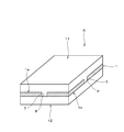
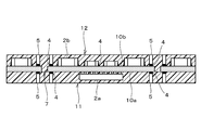
- FIG. 1 is a front sectional view showing the structure of a multilayer substrate according to one embodiment (Example 1) of the present invention
- FIG. 2 is a perspective view thereof
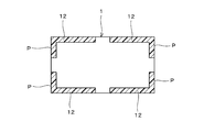
- FIG. 3 is a plan cross-sectional view for explaining an arrangement mode of regions where resin layers are bonded in the multilayer substrate according to Example 1 of the present invention.
- the multilayer substrate A includes a core substrate 1 and a surface mount component (for example, a semiconductor device) that is flip-chip mounted on one main surface 1a of the core substrate.
- Active chip component for example, a semiconductor device
- a surface-mounted component for example, a passive chip component such as a capacitor
- solder 4 to the main surface 1b of the core substrate 1
- the terminal 5 is disposed so as to seal the one and the other main surfaces 1a and 1b of the core substrate 1 and the surface-mounted components 2a and 2b disposed on both the main surfaces 1a and 1b.
- resin layers 11 and 12 having substantially the same thickness are provided. Note that the end surfaces of the straight terminals 5 are exposed from the resin layers 11 and 12 so that they can be connected to the outside.
- the resin layer 11 and the resin layer 12 are combined and integrated with each other in a predetermined region P at the peripheral edge as shown in FIGS. Specifically, as shown in FIG. 3, a portion corresponding to the central portion of each side S in the peripheral portions of the resin layers 11 and 12 formed on the upper and lower main surfaces of the core substrate 1 having a rectangular planar shape. In the recess (predetermined region) P formed in the resin layer 11, the resin layer 11 and the resin layer 12 are combined and integrated.
- a core parent substrate 10 to be divided into a plurality of core substrates 1 (FIG. 1) constituting individual multilayer substrates A (FIG. 1) is prepared. And the through-hole 7 is formed in the core mother board
- the core parent substrate 10 a plurality of ceramic layers are laminated, and a ceramic provided with an internal conductor for forming a necessary circuit and a via-hole conductor for connecting the internal conductors between the layers.
- a substrate (multilayer ceramic substrate) is used as the core parent substrate 10.
- This ceramic substrate (multilayer ceramic substrate) is formed, for example, by a method such as screen printing, with a ceramic green sheet having an inner conductor pattern formed on the surface, and further, through holes are formed and filled with conductors to form via-hole conductors for interlayer connection.
- the ceramic green sheets that are formed and the ceramic green sheets for the outer layer on which no conductor pattern is formed are appropriately combined, laminated in a predetermined order, pressed, and then fired.
- the surface electrode for mounting the surface mount component or connecting the straight terminal may be formed after firing.
- the conductor pattern is previously formed on the ceramic green sheet for the outer layer constituting the ceramic substrate. It is also possible to form the surface electrode at the same time in the step of firing the whole.
- LTCC Low Temperature Co-fired Ceramic
- the substrate that can be used as the core parent substrate 10 is not limited to a ceramic substrate, and a resin substrate or the like can also be used.
- the straight terminal 5 is connected to the other main surface 10b of the core parent substrate 10 by the solder 4 (see FIG. 4).
- the resin layer 12 is disposed on the other main surface 10b side of the core mother substrate 10 and semi-cured. At this time, the resin constituting the resin layer 12 is also filled into the through-hole 7 for joining and integrating the resin layers 11 and 12 and semi-cured.
- the material for forming the resin layer for example, a liquid epoxy resin in which an inorganic filler such as Al 2 O 3 , SiO 2 , or TiO 2 is mixed is used. And after arrange
- a phenol resin, a cyanate resin, or the like can be used as the resin for forming the resin layer, in addition to the epoxy resin. Further, a solid resin may be used instead of the liquid epoxy resin.
- a surface-mounted component in this embodiment, an active chip component such as a semiconductor device 2a is provided on the main surface (one main surface) 10a on the opposite side of the core parent substrate 10. Flip chip mounting.
- the straight terminal 5 is connected to one main surface 10a of the core parent substrate 10 by the solder 4 (see FIG. 6).
- the resin layer 11 is disposed on one main surface 10 a side of the core mother substrate 10 and is semi-cured.
- the material for forming the resin layer the same material as that used for forming the resin layer 12 described above is used, and the resin layer 11 is formed by the same method and semi-cured.
- the resin layer 11 is bonded to the resin layer 12 filled in the through hole 7.
- the resin layers 11 and 12 are still in a semi-cured state.
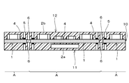
- a dividing groove 6 for dividing the core parent substrate 10 into the core individual substrates 1 is formed.
- the dividing groove 6 reaches the surface of the core parent substrate 10 from the semi-cured resin layer 11 side and the resin layer 12 side by a laser processing method, and further in the middle of the core parent substrate 10 in the thickness direction (shallow position).
- the core layer is also formed so as to reach the surface of the core parent substrate 10 from the resin layer 12 side, and further to reach the middle of the core parent substrate 10 in the thickness direction (shallow position). Since the dividing grooves 6 are formed so as to reach the middle of the core parent substrate 10 in the thickness direction (shallow position), the positions where the through holes 7 of the core parent substrate 10 are formed are shown in FIG. As described above, the dividing groove 6 reaches the resin layer inside the through hole 7 formed in the core parent substrate 10.
- the dividing groove 6 reaches the core parent substrate 10 in order to prevent the core parent substrate 10 from being divided during the manufacturing process. In some cases, it may be desirable not to enter up to 10.
- the core parent substrate 10 is placed in an oven and heated to a predetermined temperature, whereby the semi-cured resin layers 11 and 12 are fully cured.
- the main curing of the resin layers 11 and 12 is performed at 150 ° for 60 minutes.
- the core parent substrate 10 is divided into individual core substrates 1 along the dividing grooves 6. As a result, a multilayer substrate A having the structure shown in FIGS. 1 to 3 is obtained.
- the specific steps that is, the steps (1) to (9) may be switched in order.
- the steps (1) to (9) above are performed.
- (1), (2), (3), (5), (6), (4), (7), (8), (9) may be used in this order.
- the multilayer substrate A is manufactured through the manufacturing process as described above, the resin layers 11 and 12 are disposed on both main surfaces 1a and 1b of the core substrate 1, and the resin layers 11 and 12 are provided.
- the peripheral part it couple
- a multilayer substrate that is free of warpage, excellent in mountability on a mother board, and highly reliable in bonding between the core substrate and the resin layer.
- the warpage of the core substrate 1 is suppressed and prevented, disconnection of the circuit wiring formed on the multilayer substrate A can be prevented.
- the resin layers on both main surfaces of the core substrate are combined and integrated, when stress is applied to one resin layer after mounting on the motherboard, the stress is distributed to the other resin layer Thus, the stress applied to the core substrate can be weakened. For this reason, it is possible to suppress cracking and chipping of the core substrate, and to suppress characteristic fluctuations of the multilayer substrate. Moreover, it is easy to absorb bending and a bending strength improves.
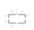
- the resin layer 11 is formed in the concave portion (predetermined region) P formed at a position corresponding to the central portion of each side (four sides) S of the core substrate 1. , 12 are combined and integrated, but the planar shape of the core substrate 1 obtained by dividing the core parent substrate 10 is configured as shown in FIGS.
- the resin layers 11 and 12 may be combined and integrated in a predetermined region P as shown in FIGS.
- a shield layer made of a conductive film may be formed on at least one resin layer.
- the shield layer when the shield layer is formed so as to cover a part of the side surface of the core substrate, there is a problem that a short circuit occurs between the shield layer and the surface mount component. Then, a short circuit can be suppressed. Further, since the shield layer has higher adhesion to the resin layer than the core substrate, the presence of the predetermined region P can increase the adhesion of the shield layer.
- a predetermined region P having a shape as shown in FIGS. 9 to 11 is formed.
- a through hole (penetrating region) 7 see FIG. 4 and the like, it can be manufactured by the same method as in the first embodiment.
- FIG. 12 (a) and 12 (b) are diagrams illustrating a state in which the resin layers 11 and 12 disposed on both main surface sides of the core substrate 1 are combined and integrated. However, in FIG. 12 (a), (b), only the core board
- the resin for forming the resin layer 12 is filled in the entire region of the through-hole 7 in one step of the manufacturing method of the multilayer substrate (step (4) above).
- the resin layer 11 is formed.
- the bonding mode of the resin layers 11 and 12 is as shown in FIG. That is, when the resin layer 11 is formed in a state in which the resin for forming the resin layer 12 is filled in the entire through hole 7, the resin layer 11 (the resin for forming the resin layer 11) becomes the through hole. 7 is bonded to the surface of the resin for forming the resin layer 12 filled in the whole, and is integrated in the subsequent curing process of the bonding layers 11 and 12, and the state as shown in FIG. Become.
- the resin for the resin layer 12 is filled up to the middle of the through hole 7, and then the resin layer 11 is formed in the middle of the through hole 7 in the step (7).
- the resin layers 11 and 12 are integrally bonded in a manner as shown in FIG.
- the bonding mode of the resin layers 11 and 12 may be any mode of FIGS. 12 (a) and 12 (b).
- FIGS. 13A and 13B are views showing a multilayer substrate B according to another embodiment (Example 2) of the present invention.
- Example 2 is another embodiment of the present invention.
- FIGS. 13A and 13B only the core substrate 1 and the resin layers 11 and 12 are shown and others are omitted for easy understanding.
- the resin layers 11 and 12 formed on both main surface sides of the core substrate 1 are connected to the core substrate 1. They are coupled together through a through-hole 17 that penetrates.
- the multilayer substrate B of Example 2 can be manufactured by a method according to the manufacturing method of Example 1 described above. That is, when the through hole is formed in the core mother board, the through hole is formed so as to penetrate the area of each core substrate included in the core mother board and not to reach the dividing line.
- the multilayer substrate B of Example 2 can be manufactured by the method according to 1.
- the present invention is not limited to the above-described embodiment in other points as well.
- Specific configurations of the core parent substrate and the core individual substrate, types and mounting modes of surface-mounted components to be mounted, resin layers Of the material constituting the core, the arrangement of the predetermined regions where the resins on both main surfaces of the core mother board should be integrated, the conditions for semi-curing and main-curing the resin layer, the core mother board as individual cores Various applications and modifications can be made within the scope of the invention with respect to a specific method for dividing into individual substrates.
- Core single substrate 1a One main surface of core single substrate 1b
- Surface mount component 4 Solder 5
- Straight terminal 6 Dividing groove 7
- Through hole 10 Core parent substrate 10a
- One main surface of core parent substrate 10b The other main surface of core parent substrate 11, 12 Resin layer A, B Multilayer substrate P Predetermined area S side
Landscapes
- Engineering & Computer Science (AREA)
- Microelectronics & Electronic Packaging (AREA)
- Manufacturing & Machinery (AREA)
- Production Of Multi-Layered Print Wiring Board (AREA)
- Structure Of Printed Boards (AREA)
Abstract
両主面側に樹脂層を備えた多層基板を製造する場合に、樹脂層の硬化工程での反りの発生を抑制することが可能で、信頼性の高い多層基板を製造する方法および反りがなく信頼性の高い多層基板を提供する。 複数のコア個基板を含み、各コア個基板を貫通する貫通孔7が形成されたコア親基板10の両主面側に表面実装部品2a,2bが実装された実装済みのコア親基板を形成し、コア親基板10を分割することにより得られる個々のコア個基板1が備える両主面側の樹脂層11,12が所定の領域Pで互いに結合して一体化した状態となるように、コア親基板の両主面に半硬化状態の樹脂層を形成し、貫通孔7を介して両主面側の樹脂層を互いに接合させた後、樹脂層を本硬化させ、その後に、コア親基板を所定の位置で分割して個々のコア個基板1に分ける。
Description
本発明は、多層基板および多層基板の製造方法に関し、詳しくは、表面実装部品が実装されたコア基板の両主面が封止用の樹脂層により封止された構造を有する多層基板およびその製造方法に関する。
多層基板の1つに、図14に示すような構成を備えた多層基板が提案されている。この多層基板は、図14に示すように、積層された複数のセラミック層からなるコア基板(セラミック多層基板)110を有し、一方の主面には、半導体装置などの能動チップ部品140が配設され、他方の主面にはコンデンサなどの受動チップ部品150が配設されている。
そして、コア基板(セラミック多層基板)110の両主面には、封止用の樹脂層120,130が形成され、下面側の樹脂層130には、表面電極121や、ビア導体122が形成されている。
この多層基板のように、コア基板(セラミック多層基板)110の両主面を樹脂層120,130により封止した構造を有する多層基板の場合、樹脂層120,130を形成する際における樹脂の硬化工程で、コア基板110と樹脂層120,130の間の膨張収縮率の差から、コア基板110に反りが発生し、多層基板をモジュール基板などに実装する際の実装信頼性が低下したり、場合によっては多層基板に配設された導体に断線が発生したりするという問題点がある。
また、コア基板110と樹脂層120,130の間の熱応力により、コア基板110と樹脂層120,130間に剥がれが生じる場合がある。
また、コア基板110と樹脂層120,130の間の熱応力により、コア基板110と樹脂層120,130間に剥がれが生じる場合がある。
本発明は、上記課題を解決するものであり、コア基板の両主面が封止用の樹脂層により封止された構造を有する多層基板を製造するにあたって、樹脂層を硬化させる工程で反りが生じることを抑制して、反りがなく、信頼性の高い多層基板を確実に製造することが可能な多層基板の製造方法を提供することを目的とする。
上記の課題を解決するため、本発明の多層基板の製造方法は、
コア個基板の両主面に配設された封止用の樹脂層を備えた多層基板の製造方法であって、
(a)複数のコア個基板を含み、各コア個基板を貫通する貫通孔が形成されたコア親基板の両主面側に、前記封止層により封止されるべき表面実装部品が実装された実装済みコア親基板を形成する工程と、
(b)下記の工程で前記コア親基板を分割することにより得られる個々のコア個基板が備える両主面側の樹脂層が所定の領域で互いに結合して一体化した状態となるように、前記コア親基板の両主面に半硬化状態の樹脂層を形成するとともに、前記貫通孔を介して両主面側の前記樹脂層を互いに接合させる樹脂層形成工程と、
(c)前記コア親基板に形成した前記半硬化状態の樹脂層を本硬化させる樹脂層硬化工程と、
(d)前記樹脂層硬化工程で本硬化させた樹脂層を備えた前記コア親基板を所定の位置で分割して個々のコア個基板に分ける分割工程と
を具備することを特徴としている。
なお、本発明において、「各コア個基板を貫通する貫通孔」とは、完全な貫通孔がコア個基板を貫通している場合と、貫通孔の一部分がコア個基板を貫通している場合(すなわち、1つの貫通孔が複数個のコア個基板にわたって、コア個基板を貫通している場合)とを含む広い概念である。
コア個基板の両主面に配設された封止用の樹脂層を備えた多層基板の製造方法であって、
(a)複数のコア個基板を含み、各コア個基板を貫通する貫通孔が形成されたコア親基板の両主面側に、前記封止層により封止されるべき表面実装部品が実装された実装済みコア親基板を形成する工程と、
(b)下記の工程で前記コア親基板を分割することにより得られる個々のコア個基板が備える両主面側の樹脂層が所定の領域で互いに結合して一体化した状態となるように、前記コア親基板の両主面に半硬化状態の樹脂層を形成するとともに、前記貫通孔を介して両主面側の前記樹脂層を互いに接合させる樹脂層形成工程と、
(c)前記コア親基板に形成した前記半硬化状態の樹脂層を本硬化させる樹脂層硬化工程と、
(d)前記樹脂層硬化工程で本硬化させた樹脂層を備えた前記コア親基板を所定の位置で分割して個々のコア個基板に分ける分割工程と
を具備することを特徴としている。
なお、本発明において、「各コア個基板を貫通する貫通孔」とは、完全な貫通孔がコア個基板を貫通している場合と、貫通孔の一部分がコア個基板を貫通している場合(すなわち、1つの貫通孔が複数個のコア個基板にわたって、コア個基板を貫通している場合)とを含む広い概念である。
また、本発明においては、前記コア個基板が備える両主面側の前記樹脂層が、周縁部の所定の領域で互いに結合して一体化するように、前記貫通孔として、前記コア親基板に含まれる各コア個基板の外周縁の一部を切り欠くような貫通孔を形成することが好ましい。
この構成を備えることにより、コア個基板が備える両主面側の樹脂層が周縁部で互いに結合して一体化するため、反りがなく、信頼性の高い多層基板を得ることができる。また、コア個基板の中央領域が樹脂層を結合させる領域として使用されないので、コア個基板の中央領域を、表面実装部品の実装領域などとして有効に利用することができる。
この構成を備えることにより、コア個基板が備える両主面側の樹脂層が周縁部で互いに結合して一体化するため、反りがなく、信頼性の高い多層基板を得ることができる。また、コア個基板の中央領域が樹脂層を結合させる領域として使用されないので、コア個基板の中央領域を、表面実装部品の実装領域などとして有効に利用することができる。
また、前記コア個基板が備える両主面側の前記樹脂層が、前記コア個基板を貫通する領域において互いに結合して一体化するように、前記貫通孔として、前記コア親基板に含まれる各コア個基板の領域内を貫通する貫通孔を形成することが好ましい。
この構成を備えることにより、コア個基板が備える両主面側の前記樹脂層が、コア個基板の貫通部で確実に結合して一体化するため、反りがなく、信頼性の高い多層基板を得ることができる。
この構成を備えることにより、コア個基板が備える両主面側の前記樹脂層が、コア個基板の貫通部で確実に結合して一体化するため、反りがなく、信頼性の高い多層基板を得ることができる。
また、前記(b)の樹脂層形成工程と、前記(c)の樹脂層硬化工程の間に、前記コア親基板を前記コア個基板に分割するための分割用溝として、前記半硬化状態の樹脂層側から前記コア親基板に達する溝を形成する工程を備えていることが好ましい。
この構成を備えることにより、樹脂の本硬化後の個々のコア個基板への分割を効率よく行うことが可能になり、好ましい。
この構成を備えることにより、樹脂の本硬化後の個々のコア個基板への分割を効率よく行うことが可能になり、好ましい。
また、本発明の多層基板は、
コア個基板と、
コア個基板の両主面に実装された表面実装部品と、
前記コア個基板の両主面に、前記表面実装部品を封止するように配設された樹脂層であって、所定の領域で互いに結合して一体化した樹脂層と
を具備することを特徴としている。
コア個基板と、
コア個基板の両主面に実装された表面実装部品と、
前記コア個基板の両主面に、前記表面実装部品を封止するように配設された樹脂層であって、所定の領域で互いに結合して一体化した樹脂層と
を具備することを特徴としている。
本発明の多層基板においては、前記コア個基板が備える両主面側の前記樹脂層が、周縁部の所定の領域で互いに結合して一体化していることが好ましい。
この構成を備えることにより、コア個基板の周縁部で樹脂層が確実に結合された、反りがなく、信頼性の高い多層基板を得ることができる。また、コア個基板の中央領域が樹脂層を結合させる領域として使用されないので、コア個基板の中央領域を表面実装部品の実装領域などとして有効に利用することができる。
この構成を備えることにより、コア個基板の周縁部で樹脂層が確実に結合された、反りがなく、信頼性の高い多層基板を得ることができる。また、コア個基板の中央領域が樹脂層を結合させる領域として使用されないので、コア個基板の中央領域を表面実装部品の実装領域などとして有効に利用することができる。
また、前記コア個基板が備える両主面側の前記樹脂層が、前記コア個基板を貫通する領域において互いに結合して一体化していることが好ましい。
この構成を備えることにより、コア個基板の貫通部で樹脂層が確実に結合された、反りがなく、信頼性の高い多層基板を得ることができる。
この構成を備えることにより、コア個基板の貫通部で樹脂層が確実に結合された、反りがなく、信頼性の高い多層基板を得ることができる。
本発明の多層基板の製造方法は、樹脂層を本硬化させる硬化工程では、コア親基板に含まれるコア個基板のそれぞれにおいて、両主面側に位置する半硬化状態の樹脂層が一体化した状態で本硬化することになるため、コア個基板に反りが生じることを防止して、反りがなく、マザーボードへの実装性に優れた、信頼性の高い多層基板を得ることが可能になる。
また、コア個基板の両主面側の樹脂層が結合して一体化していることから、コア個基板と樹脂層との接合信頼性の高い多層基板を得ることができる。
また、本発明の多層基板は、コア個基板の両主面に配設され所定の領域で互いに結合して一体化した樹脂層とを備えているので、反りがなく、マザーボードへの実装性に優れた、信頼性の高い多層基板を提供することができる。
また、コア個基板の両主面側の樹脂層が結合して一体化していることから、コア個基板と樹脂層との接合信頼性の高い多層基板を提供することができる。
また、コア個基板の両主面側の樹脂層が結合して一体化していることから、一方の樹脂層に応力がかかったときに、他方の樹脂層に応力が分散され、コア個基板にかかる応力を弱めることができる。そのためコア個基板の割れや欠けを抑制でき、多層基板の特性変動を抑制することができる。
また、コア個基板の両主面側の樹脂層が結合して一体化していることから、コア個基板と樹脂層との接合信頼性の高い多層基板を提供することができる。
また、コア個基板の両主面側の樹脂層が結合して一体化していることから、一方の樹脂層に応力がかかったときに、他方の樹脂層に応力が分散され、コア個基板にかかる応力を弱めることができる。そのためコア個基板の割れや欠けを抑制でき、多層基板の特性変動を抑制することができる。
以下に本発明の実施例を示して、本発明の特徴とするところをさらに詳しく説明する。
図1は本発明の一実施例(実施例1)にかかる多層基板の構成を示す正面断面図、図2はその斜視図である。また、図3は本発明の実施例1にかかる多層基板における樹脂層を結合させる領域の配設態様を説明するための平面断面図である。
この実施例1の多層基板Aは、図1および2に示すように、コア個基板1と、コア個基板の一方の主面1aにフリップチップ実装された表面実装部品(例えば、半導体装置などの能動チップ部品)2aと、他方の主面1bにはんだ付け実装された表面実装部品(例えば、コンデンサなどの受動チップ部品)2bと、コア個基板1の主面1bにはんだ4により接続されたストレート端子5と、コア個基板1の一方および他方の両主面1a,1b、および、両主面1a,1b上に配設された表面実装部品2a,2bなどを封止するように配設された、ほぼ同等の厚みを有する樹脂層11,12とを具備している。なお、ストレート端子5は外部に接続することができるように端面が樹脂層11,12から露出している。
そして、この実施例1の多層基板Aにおいては、樹脂層11および樹脂層12は、図1,2に示すように、周縁部の所定の領域Pにおいて、互いに結合して一体化されている。
具体的には、図3に示すように、平面形状が長方形のコア個基板1の上下両主面に形成された樹脂層11,12の周縁部における、各辺Sの中央部に相当する箇所に形成された凹部(所定の領域)Pにおいて、樹脂層11と樹脂層12とが結合して、一体化している。
具体的には、図3に示すように、平面形状が長方形のコア個基板1の上下両主面に形成された樹脂層11,12の周縁部における、各辺Sの中央部に相当する箇所に形成された凹部(所定の領域)Pにおいて、樹脂層11と樹脂層12とが結合して、一体化している。
次に、この多層基板Aの製造方法を、図4~図8を参照しつつ説明する。
(1)まず、個々の多層基板A(図1)を構成する複数のコア個基板1(図1)に分割されることになるコア親基板10を用意する。そして、コア親基板10に、上述の樹脂層11,12を結合させて一体化するための領域として貫通孔7を形成する。
なお、この実施例では、コア親基板10として、複数のセラミック層が積層され、内部に、必要な回路を形成するための内部導体や内部導体を層間接続するためのビアホール導体などを備えたセラミック基板(多層セラミック基板)を用いている。
(1)まず、個々の多層基板A(図1)を構成する複数のコア個基板1(図1)に分割されることになるコア親基板10を用意する。そして、コア親基板10に、上述の樹脂層11,12を結合させて一体化するための領域として貫通孔7を形成する。
なお、この実施例では、コア親基板10として、複数のセラミック層が積層され、内部に、必要な回路を形成するための内部導体や内部導体を層間接続するためのビアホール導体などを備えたセラミック基板(多層セラミック基板)を用いている。
このセラミック基板(多層セラミック基板)は、例えば、スクリーン印刷などの方法で、表面に内部導体パターンを形成したセラミックグリーンシート、さらに貫通孔を形成した後に導体を充填して層間接続用のビアホール導体を形成したセラミックグリーンシート、導体パターンの形成されていない外層用のセラミックグリーンシートなどを適宜組み合わせて所定の順序で積層し、圧着した後、焼成する方法などによって製造されるものである。
なお、表面実装部品を搭載したり、ストレート端子を接続したりするための表面電極は、焼成後に形成してもよく、場合によっては、セラミック基板を構成する外層用のセラミックグリーンシートに予め導体パターンを形成しておいて、全体を焼成する工程で同時に表面電極が形成されるようにすることも可能である。
ただし、セラミック基板の製造方法や具体的な構成には特別の制約はなく、公知の種々の方法で製造された、種々の構成を有するセラミック基板を用いることができる。
また、セラミック基板を用いる場合、特に焼成低温の低い、LTCC(低温同時焼成セラミックス:Low Temperature Co-fired Ceramics)基板を用いることも可能である。
また、コア親基板10として用いることが可能な基板は、セラミック基板に限られるものではなく、樹脂基板などを用いることも可能である。
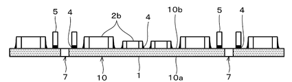
(2)それから、図4に示すように、コア親基板10の一方の主面10aと他方の主面10bのうち、他方の主面10b上に、表面実装部品(この実施例では、例えば、コンデンサなどの受動チップ部品)2bをはんだ付け実装などの方法で実装する。
(3)次いで、ストレート端子5をはんだ4によりコア親基板10の他方の主面10bに接続する(図4参照)。
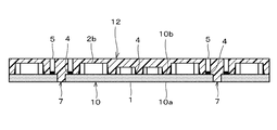
(4)それから、図5に示すように、コア親基板10の他方の主面10b側に、樹脂層12を配設し、半硬化させる。このとき、樹脂層12を構成する樹脂を、上述の樹脂層11,12を結合させて一体化するための貫通孔7にも充填し、半硬化させる。
ここでは、樹脂層形成用の材料として、例えば、Al2O3、SiO2、TiO2など無機フィラーが混合された液状エポキシ樹脂を用いる。そして、これをコア親基板10の他方の主面10b側に配設した後、100℃で90分熱処理することにより半硬化させる。なお、後述のように、樹脂層11,12の本硬化は、150°、60分の条件で行う。
本発明においては、樹脂層形成用の樹脂として、エポキシ樹脂以外にも、フェノール樹脂、シアネート樹脂などを用いることができる。また、液状エポキシ樹脂に替えて、固形樹脂を用いてもよい。
本発明においては、樹脂層形成用の樹脂として、エポキシ樹脂以外にも、フェノール樹脂、シアネート樹脂などを用いることができる。また、液状エポキシ樹脂に替えて、固形樹脂を用いてもよい。
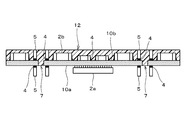
(5)次に、図6に示すように、コア親基板10の反対側の主面(一方の主面)10aに表面実装部品(この実施例では、半導体装置などの能動チップ部品)2aをフリップチップ実装する。
(6)次いで、ストレート端子5をはんだ4によりコア親基板10の一方の主面10aに接続する(図6参照)。
(7)それから、図7に示すように、コア親基板10の一方の主面10a側に、樹脂層11を配設し、半硬化させる。このとき、樹脂層形成用の材料として、上述の樹脂層12を形成するのに用いた材料と同じ材料を用いて、同様の方法で樹脂層11を形成し、半硬化させる。
この工程において、樹脂層11は、貫通孔7内に充填された樹脂層12と接合する。ただし、この段階では、樹脂層11,12は、まだ半硬化の状態にある。
この工程において、樹脂層11は、貫通孔7内に充填された樹脂層12と接合する。ただし、この段階では、樹脂層11,12は、まだ半硬化の状態にある。
(8)その後、図8に示すように、コア親基板10をコア個基板1に分割するための分割用溝6を形成する。
分割用溝6は、レーザ加工法により、半硬化状態の樹脂層11側および樹脂層12側から、コア親基板10の表面に達し、さらに、コア親基板10の厚み方向の途中(浅い位置)にまで達するように形成するとともに、樹脂層12側からも、コア親基板10の表面に達し、さらに、コア親基板10の厚み方向の途中(浅い位置)にまで達するように形成する。分割用溝6が、コア親基板10の厚み方向の途中(浅い位置)にまで達するように形成されることから、コア親基板10の貫通孔7が形成された位置においては、図8に示すように、分割用溝6が、コア親基板10に形成された貫通孔7の内部の樹脂層にまで達する。
分割用溝6は、レーザ加工法により、半硬化状態の樹脂層11側および樹脂層12側から、コア親基板10の表面に達し、さらに、コア親基板10の厚み方向の途中(浅い位置)にまで達するように形成するとともに、樹脂層12側からも、コア親基板10の表面に達し、さらに、コア親基板10の厚み方向の途中(浅い位置)にまで達するように形成する。分割用溝6が、コア親基板10の厚み方向の途中(浅い位置)にまで達するように形成されることから、コア親基板10の貫通孔7が形成された位置においては、図8に示すように、分割用溝6が、コア親基板10に形成された貫通孔7の内部の樹脂層にまで達する。
なお、コア親基板10が薄い場合や脆い材料の場合は、製造工程の途中で分割されてしまうことを防止するため、分割用溝6がコア親基板10に達してはいるが、コア親基板10にまでは入り込まないようにすることが望ましい場合もある。
(9)次に、コア親基板10をオーブンに入れて所定の温度に加熱することにより、半硬化状態の樹脂層11,12を本硬化させる。なお、樹脂層11,12の本硬化は150°、60分の条件で行う。
それから、コア親基板10を分割用溝6に沿って個々のコア個基板1に分割する。これにより、図1~3にその構成を示すような構造を有する多層基板Aが得られる。
それから、コア親基板10を分割用溝6に沿って個々のコア個基板1に分割する。これにより、図1~3にその構成を示すような構造を有する多層基板Aが得られる。
なお、上述の多層基板Aを製造する場合においては、具体的な工程、すなわち、上記(1)~(9)の工程はその順序が入れ替わる場合もある。
例えば、上記(1)~(9)の工程を、
(1),(2),(3),(5),(6),(4),(7),(8),(9)の順としたりすることも可能である。
さらに、上述の例と異なる態様で上記(1)~(9)の各工程を実施することも可能である。
例えば、上記(1)~(9)の工程を、
(1),(2),(3),(5),(6),(4),(7),(8),(9)の順としたりすることも可能である。
さらに、上述の例と異なる態様で上記(1)~(9)の各工程を実施することも可能である。
この多層基板Aは、上述のような製造工程を経て製造されるとともに、コア個基板1の両主面1a,1b側に樹脂層11,12が配設され、かつ、樹脂層11,12がその周縁部における、各辺Sの中央部に相当する箇所に形成された凹部(上述の貫通孔7が分割されて形成された所定の領域)P(図3)において結合、一体化されているので、樹脂層11,12の硬化工程でコア個基板1に反りが生じることを効果的に抑制、防止することができる。
その結果、反りがなく、マザーボードへの実装性に優れ、かつ、コア個基板と樹脂層との接合信頼性の高い多層基板を得ることが可能になる。
その結果、反りがなく、マザーボードへの実装性に優れ、かつ、コア個基板と樹脂層との接合信頼性の高い多層基板を得ることが可能になる。
また、コア個基板1の反りが抑制、防止されることから、多層基板Aに形成された回路配線などの断線を防止することができる。
また、コア個基板の両主面側の樹脂層が結合して一体化していることから、マザーボードへの実装後に、一方の樹脂層に応力がかかったときに、他方の樹脂層に応力が分散され、コア個基板にかかる応力を弱めることができる。そのためコア個基板の割れや欠けを抑制でき、多層基板の特性変動を抑制することができる。また撓みを吸収しやすく、撓み強度も向上する。
また、コア個基板の両主面側の樹脂層が結合して一体化していることから、マザーボードへの実装後に、一方の樹脂層に応力がかかったときに、他方の樹脂層に応力が分散され、コア個基板にかかる応力を弱めることができる。そのためコア個基板の割れや欠けを抑制でき、多層基板の特性変動を抑制することができる。また撓みを吸収しやすく、撓み強度も向上する。
なお、上記の実施例では、図3に示すように、コア個基板1の各辺(4つの辺)Sの中央部に相当する箇所に形成された凹部(所定の領域)Pにおいて樹脂層11,12を結合、一体化させているが、コア親基板10を分割することにより得られるコア個基板1の平面形状が、図9,10,および11に示すような形状になるように構成し、かつ、樹脂層11,12を、図9,10,および11に示すような所定の領域Pで結合、一体化させるように構成することも可能である。
特に、図10,11のように、コア個基板の角部を覆うように所定の領域Pが配置されるとコア個基板の割れや欠けを抑制することができる。
なお、図1において、少なくとも一方の樹脂層に導電性膜からなるシールド層を形成してもよい。特にコア個基板の側面の一部にもかかるようにシールド層を形成する場合には、シールド層と表面実装部品間でショートするという問題があるが、そのような場所に所定の領域Pを配置すると、ショートを抑制することができる。また、シールド層は、コア個基板より樹脂層との密着性が高いので、所定の領域Pがあることにより、シールド層の密着性を高めることができる。
特に、図10,11のように、コア個基板の角部を覆うように所定の領域Pが配置されるとコア個基板の割れや欠けを抑制することができる。
なお、図1において、少なくとも一方の樹脂層に導電性膜からなるシールド層を形成してもよい。特にコア個基板の側面の一部にもかかるようにシールド層を形成する場合には、シールド層と表面実装部品間でショートするという問題があるが、そのような場所に所定の領域Pを配置すると、ショートを抑制することができる。また、シールド層は、コア個基板より樹脂層との密着性が高いので、所定の領域Pがあることにより、シールド層の密着性を高めることができる。
なお、図9~11の構成の多層基板は、コア親基板10に、それを各コア個基板1に分割したときに、図9~11に示すような形状を有する所定の領域Pが形成されるような貫通孔(貫通領域)7(図4など参照)を形成することにより、上記実施例1の場合と同じ方法で製造することができる。
また、図12(a),(b)はコア個基板1の両主面側に配設された樹脂層11,12を結合、一体化させた状態を説明する図である。ただし、図12(a),(b)では、理解を容易にするため、コア個基板1と樹脂層11,12のみを示し、他は省略している。
上記実施例では、多層基板の製造方法の一工程(上記(4)の工程)で、貫通孔7の全領域に樹脂層12を形成するための樹脂を充填し、その後、上記(7)の工程で、樹脂層11を形成するようにしているが、その場合、樹脂層11,12の結合態様は、図12(a)に示すようになる。すなわち、樹脂層12を構成するための樹脂が貫通孔7の全体に充填されている状態で、樹脂層11が形成されることにより、樹脂層11(を形成するための樹脂)が、貫通孔7の全体に充填された樹脂層12を形成するための樹脂の表面と接合し、その後の接合層11,12の本硬化の工程で一体化して、図12(a)に示すような状態となる。
一方、上記(4)の工程で、貫通孔7の途中まで樹脂層12用の樹脂を充填し、その後、上記(7)の工程で、樹脂層11を形成する際に、貫通孔7の途中まで樹脂層11を形成するための樹脂が充填されるようにした場合、図12(b)に示すような態様で樹脂層11,12が一体に結合されることになる。
本発明において、樹脂層11,12の結合態様は、図12(a),(b)のいずれの態様であってもよい。
図13(a),(b)は、本発明の他の実施例(実施例2)にかかる多層基板Bを示す図である。なお、図13(a),(b)では、理解を容易にするため、コア個基板1と樹脂層11,12のみを示し、他は省略している。
図13(a),(b)に示すように、この実施例2の多層基板Bにおいては、コア個基板1の両主面側に形成された樹脂層11,12が、コア個基板1を貫通する貫通孔17を介して、一体に結合されている。
この実施例2の構成の場合にも、上記実施例1の場合と同様の効果を得ることができる。
なお、この実施例2の多層基板Bは、上記実施例1の製造方法に準じる方法で製造することができる。すなわち、コア親基板に貫通孔を形成する際に、コア親基板に含まれる各コア個基板の領域内を貫通するとともに、分割ラインにかからないように、貫通孔を形成することにより、上記実施例1の場合に準じる方法でこの実施例2の多層基板Bを製造することができる。
なお、本発明は、さらにその他の点においても上記実施例に限定されるものではなく、コア親基板やコア個基板の具体的な構成、実装される表面実装部品の種類や実装態様、樹脂層を構成する材料の種類、コア親基板の両主面側の樹脂を一体化させるべき所定の領域の配設態様、樹脂層を半硬化および本硬化させる際の条件、コア親基板を個々のコア個基板に分割する際の具体的な方法などに関し、発明の範囲内において、種々の応用、変形を加えることができる。
1 コア個基板
1a コア個基板の一方の主面
1b コア個基板の他方の主面
2a,2b 表面実装部品
4 はんだ
5 ストレート端子
6 分割用溝
7 貫通孔
10 コア親基板
10a コア親基板の一方の主面
10b コア親基板の他方の主面
11,12 樹脂層
A,B 多層基板
P 所定の領域
S 辺
1a コア個基板の一方の主面
1b コア個基板の他方の主面
2a,2b 表面実装部品
4 はんだ
5 ストレート端子
6 分割用溝
7 貫通孔
10 コア親基板
10a コア親基板の一方の主面
10b コア親基板の他方の主面
11,12 樹脂層
A,B 多層基板
P 所定の領域
S 辺
Claims (7)
- コア個基板の両主面に配設された封止用の樹脂層を備えた多層基板の製造方法であって、
(a)複数のコア個基板を含み、各コア個基板を貫通する貫通孔が形成されたコア親基板の両主面側に、前記封止層により封止されるべき表面実装部品が実装された実装済みコア親基板を形成する工程と、
(b)下記の工程で前記コア親基板を分割することにより得られる個々のコア個基板が備える両主面側の樹脂層が所定の領域で互いに結合して一体化した状態となるように、前記コア親基板の両主面に半硬化状態の樹脂層を形成するとともに、前記貫通孔を介して両主面側の前記樹脂層を互いに接合させる樹脂層形成工程と、
(c)前記コア親基板に形成した前記半硬化状態の樹脂層を本硬化させる樹脂層硬化工程と、
(d)前記樹脂層硬化工程で本硬化させた樹脂層を備えた前記コア親基板を所定の位置で分割して個々のコア個基板に分ける分割工程と
を具備することを特徴とする多層基板の製造方法。 - 前記コア個基板が備える両主面側の前記樹脂層が、周縁部の所定の領域で互いに結合して一体化するように、前記貫通孔として、前記コア親基板に含まれる各コア個基板の外周縁の一部を切り欠くような貫通孔を形成することを特徴とする請求項1記載の多層基板の製造方法。
- 前記コア個基板が備える両主面側の前記樹脂層が、前記コア個基板を貫通する領域において互いに結合して一体化するように、前記貫通孔として、前記コア親基板に含まれる各コア個基板の領域内を貫通する貫通孔を形成することを特徴とする請求項1記載の多層基板の製造方法。
- 前記(b)の樹脂層形成工程と、前記(c)の樹脂層硬化工程の間に、前記コア親基板を前記コア個基板に分割するための分割用溝として、前記半硬化状態の樹脂層側から前記コア親基板に達する溝を形成する工程を備えていることを特徴とする請求項1~3のいずれかに記載の多層基板の製造方法。
- コア個基板と、
コア個基板の両主面に実装された表面実装部品と、
前記コア個基板の両主面に、前記表面実装部品を封止するように配設された樹脂層であって、所定の領域で互いに結合して一体化した樹脂層と
を具備することを特徴とする多層基板。 - 前記コア個基板が備える両主面側の前記樹脂層が、周縁部の所定の領域で互いに結合して一体化していることを特徴とする請求項5記載の多層基板。
- 前記コア個基板が備える両主面側の前記樹脂層が、前記コア個基板を貫通する領域において互いに結合して一体化していることを特徴とする請求項5記載の多層基板。
Priority Applications (2)
| Application Number | Priority Date | Filing Date | Title |
|---|---|---|---|
| JP2013518150A JP5614566B2 (ja) | 2011-06-03 | 2012-05-31 | 多層基板の製造方法および多層基板 |
| US14/094,240 US9451700B2 (en) | 2011-06-03 | 2013-12-02 | Method for producing multi-layer substrate and multi-layer substrate |
Applications Claiming Priority (2)
| Application Number | Priority Date | Filing Date | Title |
|---|---|---|---|
| JP2011125003 | 2011-06-03 | ||
| JP2011-125003 | 2011-06-03 |
Related Child Applications (1)
| Application Number | Title | Priority Date | Filing Date |
|---|---|---|---|
| US14/094,240 Continuation US9451700B2 (en) | 2011-06-03 | 2013-12-02 | Method for producing multi-layer substrate and multi-layer substrate |
Publications (1)
| Publication Number | Publication Date |
|---|---|
| WO2012165530A1 true WO2012165530A1 (ja) | 2012-12-06 |
Family
ID=47259382
Family Applications (1)
| Application Number | Title | Priority Date | Filing Date |
|---|---|---|---|
| PCT/JP2012/064044 Ceased WO2012165530A1 (ja) | 2011-06-03 | 2012-05-31 | 多層基板の製造方法および多層基板 |
Country Status (3)
| Country | Link |
|---|---|
| US (1) | US9451700B2 (ja) |
| JP (1) | JP5614566B2 (ja) |
| WO (1) | WO2012165530A1 (ja) |
Cited By (1)
| Publication number | Priority date | Publication date | Assignee | Title |
|---|---|---|---|---|
| WO2024048760A1 (ja) * | 2022-09-02 | 2024-03-07 | 株式会社レゾナック | 半導体パッケージを製造する方法 |
Families Citing this family (11)
| Publication number | Priority date | Publication date | Assignee | Title |
|---|---|---|---|---|
| US10833024B2 (en) * | 2016-10-18 | 2020-11-10 | Advanced Semiconductor Engineering, Inc. | Substrate structure, packaging method and semiconductor package structure |
| WO2018110397A1 (ja) * | 2016-12-14 | 2018-06-21 | 株式会社村田製作所 | モジュール |
| CN110140433B (zh) * | 2016-12-15 | 2021-10-12 | 株式会社村田制作所 | 电子模块以及电子模块的制造方法 |
| US10910233B2 (en) | 2018-04-11 | 2021-02-02 | Advanced Semiconductor Engineering, Inc. | Semiconductor device package and method of manufacturing the same |
| US10755994B2 (en) | 2018-10-29 | 2020-08-25 | Advanced Semiconductor Engineering, Inc. | Semiconductor package structure and semiconductor substrate |
| WO2021131775A1 (ja) * | 2019-12-27 | 2021-07-01 | 株式会社村田製作所 | モジュール |
| US20210233868A1 (en) * | 2020-01-28 | 2021-07-29 | Advanced Semiconductor Engineering, Inc. | Semiconductor device package and method for manufacturing the same |
| CN114126211B (zh) * | 2020-08-25 | 2025-01-03 | 华为技术有限公司 | 一种封装模块以及电子设备 |
| KR102900134B1 (ko) | 2020-12-22 | 2025-12-17 | 삼성전자주식회사 | 스트립 기판 및 반도체 패키지 |
| KR102943789B1 (ko) | 2021-05-13 | 2026-03-24 | 삼성전자주식회사 | 패키지 기판을 가지는 반도체 패키지 |
| US12142402B2 (en) * | 2021-06-10 | 2024-11-12 | SanDisk Technologies, Inc. | Monolithic surface mount passive component |
Citations (9)
| Publication number | Priority date | Publication date | Assignee | Title |
|---|---|---|---|---|
| JPS59109173U (ja) * | 1983-01-14 | 1984-07-23 | アルプス電気株式会社 | 樹脂塗装絶縁基板 |
| JP2001135920A (ja) * | 1999-11-09 | 2001-05-18 | Matsushita Electric Ind Co Ltd | 樹脂成形回路基板及びその製造方法 |
| JP2003086925A (ja) * | 2001-09-12 | 2003-03-20 | Matsushita Electric Ind Co Ltd | 防湿構造付プリント基板、及びその製造方法 |
| JP2003112335A (ja) * | 2001-10-02 | 2003-04-15 | Sony Corp | 樹脂封止型成形部品の製造方法および樹脂封止型成形部品 |
| JP2005191090A (ja) * | 2003-12-24 | 2005-07-14 | Ngk Spark Plug Co Ltd | 配線基板の製造方法および配線基板素材 |
| JP2005311201A (ja) * | 2004-04-23 | 2005-11-04 | Matsushita Electric Works Ltd | 部品内蔵回路板及びその製造方法 |
| WO2009066504A1 (ja) * | 2007-11-20 | 2009-05-28 | Murata Manufacturing Co., Ltd. | 部品内蔵モジュール |
| WO2009139121A1 (ja) * | 2008-05-13 | 2009-11-19 | パナソニック株式会社 | 電子部品 |
| JP2010016291A (ja) * | 2008-07-07 | 2010-01-21 | Shinko Electric Ind Co Ltd | 配線基板及び半導体装置の製造方法 |
Family Cites Families (6)
| Publication number | Priority date | Publication date | Assignee | Title |
|---|---|---|---|---|
| US20040126547A1 (en) * | 2002-12-31 | 2004-07-01 | Coomer Boyd L. | Methods for performing substrate imprinting using thermoset resin varnishes and products formed therefrom |
| KR100753499B1 (ko) | 2004-02-13 | 2007-08-31 | 가부시키가이샤 무라타 세이사쿠쇼 | 전자 부품 및 그 제조 방법 |
| JP2008166603A (ja) | 2006-12-28 | 2008-07-17 | Nippon Densan Corp | プリント配線部材、部品搭載基板、ブラシレスモータ、ディスク駆動装置、及び部品搭載基板の製造方法 |
| JP2008277392A (ja) | 2007-04-26 | 2008-11-13 | Kyocera Corp | 部品内蔵基板およびその製造方法 |
| JP2009188218A (ja) | 2008-02-07 | 2009-08-20 | Murata Mfg Co Ltd | 多層基板 |
| DE112009000666T5 (de) * | 2008-03-24 | 2011-07-28 | Murata Mfg. Co., Ltd., Kyoto | Verfahren zum Herstellen eines Elektronikkomponentenmoduls |
-
2012
- 2012-05-31 WO PCT/JP2012/064044 patent/WO2012165530A1/ja not_active Ceased
- 2012-05-31 JP JP2013518150A patent/JP5614566B2/ja active Active
-
2013
- 2013-12-02 US US14/094,240 patent/US9451700B2/en active Active
Patent Citations (9)
| Publication number | Priority date | Publication date | Assignee | Title |
|---|---|---|---|---|
| JPS59109173U (ja) * | 1983-01-14 | 1984-07-23 | アルプス電気株式会社 | 樹脂塗装絶縁基板 |
| JP2001135920A (ja) * | 1999-11-09 | 2001-05-18 | Matsushita Electric Ind Co Ltd | 樹脂成形回路基板及びその製造方法 |
| JP2003086925A (ja) * | 2001-09-12 | 2003-03-20 | Matsushita Electric Ind Co Ltd | 防湿構造付プリント基板、及びその製造方法 |
| JP2003112335A (ja) * | 2001-10-02 | 2003-04-15 | Sony Corp | 樹脂封止型成形部品の製造方法および樹脂封止型成形部品 |
| JP2005191090A (ja) * | 2003-12-24 | 2005-07-14 | Ngk Spark Plug Co Ltd | 配線基板の製造方法および配線基板素材 |
| JP2005311201A (ja) * | 2004-04-23 | 2005-11-04 | Matsushita Electric Works Ltd | 部品内蔵回路板及びその製造方法 |
| WO2009066504A1 (ja) * | 2007-11-20 | 2009-05-28 | Murata Manufacturing Co., Ltd. | 部品内蔵モジュール |
| WO2009139121A1 (ja) * | 2008-05-13 | 2009-11-19 | パナソニック株式会社 | 電子部品 |
| JP2010016291A (ja) * | 2008-07-07 | 2010-01-21 | Shinko Electric Ind Co Ltd | 配線基板及び半導体装置の製造方法 |
Cited By (4)
| Publication number | Priority date | Publication date | Assignee | Title |
|---|---|---|---|---|
| WO2024048760A1 (ja) * | 2022-09-02 | 2024-03-07 | 株式会社レゾナック | 半導体パッケージを製造する方法 |
| WO2024048762A1 (ja) * | 2022-09-02 | 2024-03-07 | 株式会社レゾナック | 半導体パッケージを製造する方法 |
| WO2024048763A1 (ja) * | 2022-09-02 | 2024-03-07 | 株式会社レゾナック | 半導体パッケージを製造する方法 |
| WO2024047872A1 (ja) * | 2022-09-02 | 2024-03-07 | 株式会社レゾナック | 電子部品装置を製造する方法 |
Also Published As
| Publication number | Publication date |
|---|---|
| JP5614566B2 (ja) | 2014-10-29 |
| JPWO2012165530A1 (ja) | 2015-02-23 |
| US20140085843A1 (en) | 2014-03-27 |
| US9451700B2 (en) | 2016-09-20 |
Similar Documents
| Publication | Publication Date | Title |
|---|---|---|
| JP5614566B2 (ja) | 多層基板の製造方法および多層基板 | |
| JP6671441B2 (ja) | 電子部品収納用パッケージ、多数個取り配線基板、電子装置および電子モジュール | |
| WO2012023332A1 (ja) | 電子部品及びその製造方法 | |
| CN103632982A (zh) | 配线板及配线板的制造方法 | |
| WO2006043474A1 (ja) | 複合多層基板及びその製造方法 | |
| KR20150054171A (ko) | 인쇄회로기판 및 그 제조방법 | |
| WO2010150820A1 (ja) | 多数個取り配線基板および配線基板ならびに電子装置 | |
| KR100495211B1 (ko) | 세라믹 다층기판 및 그 제조방법 | |
| WO2019181761A1 (ja) | 高周波モジュール | |
| WO2011078349A1 (ja) | 多数個取り配線基板および配線基板ならびに電子装置 | |
| CN112020771A (zh) | 电子元件安装用基板、电子装置以及电子模块 | |
| JP4725817B2 (ja) | 複合基板の製造方法 | |
| KR100952171B1 (ko) | 회로 모듈 및 이 회로 모듈을 사용한 회로 장치 | |
| CN114126206B (zh) | 印制电路板及其制作方法、板级架构和电子设备 | |
| JP2008042064A (ja) | セラミック配線基板とそれを用いた光学デバイス装置、パッケージおよびセラミック配線基板の製造方法 | |
| JP2008112790A (ja) | 半導体パッケージおよびその製造方法 | |
| WO2012165111A1 (ja) | 多層基板の製造方法および多層基板 | |
| CN107615893B (zh) | 布线基板、电子装置以及电子模块 | |
| KR20090051627A (ko) | 다층 세라믹 기판 및 그의 제조방법 | |
| JP2011049354A (ja) | 電子装置 | |
| JP4752612B2 (ja) | 突起電極付き回路基板の製造方法 | |
| JP6332474B2 (ja) | セラミック基板、電子部品およびセラミック基板の製造方法 | |
| JPH0342860A (ja) | フレキシブルプリント配線板 | |
| JP2013110299A (ja) | 複合モジュール | |
| TWI718860B (zh) | 多層印刷電路板的製造方法 |
Legal Events
| Date | Code | Title | Description |
|---|---|---|---|
| 121 | Ep: the epo has been informed by wipo that ep was designated in this application |
Ref document number: 12792987 Country of ref document: EP Kind code of ref document: A1 |
|
| ENP | Entry into the national phase |
Ref document number: 2013518150 Country of ref document: JP Kind code of ref document: A |
|
| NENP | Non-entry into the national phase |
Ref country code: DE |
|
| 122 | Ep: pct application non-entry in european phase |
Ref document number: 12792987 Country of ref document: EP Kind code of ref document: A1 |