WO2012164845A1 - ワイヤレス受電装置、ワイヤレス給電装置およびワイヤレス給電システム、自動チューニング補助回路 - Google Patents
ワイヤレス受電装置、ワイヤレス給電装置およびワイヤレス給電システム、自動チューニング補助回路 Download PDFInfo
- Publication number
- WO2012164845A1 WO2012164845A1 PCT/JP2012/003190 JP2012003190W WO2012164845A1 WO 2012164845 A1 WO2012164845 A1 WO 2012164845A1 JP 2012003190 W JP2012003190 W JP 2012003190W WO 2012164845 A1 WO2012164845 A1 WO 2012164845A1
- Authority
- WO
- WIPO (PCT)
- Prior art keywords
- wireless power
- switch
- terminal
- automatic tuning
- assist circuit
- Prior art date
- Legal status (The legal status is an assumption and is not a legal conclusion. Google has not performed a legal analysis and makes no representation as to the accuracy of the status listed.)
- Ceased
Links
Images









Classifications
-
- H—ELECTRICITY
- H04—ELECTRIC COMMUNICATION TECHNIQUE
- H04B—TRANSMISSION
- H04B5/00—Near-field transmission systems, e.g. inductive or capacitive transmission systems
- H04B5/20—Near-field transmission systems, e.g. inductive or capacitive transmission systems characterised by the transmission technique; characterised by the transmission medium
- H04B5/24—Inductive coupling
-
- H—ELECTRICITY
- H01—ELECTRIC ELEMENTS
- H01F—MAGNETS; INDUCTANCES; TRANSFORMERS; SELECTION OF MATERIALS FOR THEIR MAGNETIC PROPERTIES
- H01F38/00—Adaptations of transformers or inductances for specific applications or functions
- H01F38/14—Inductive couplings
-
- H—ELECTRICITY
- H02—GENERATION; CONVERSION OR DISTRIBUTION OF ELECTRIC POWER
- H02J—ELECTRIC POWER NETWORKS; CIRCUIT ARRANGEMENTS OR SYSTEMS FOR SUPPLYING OR DISTRIBUTING ELECTRIC POWER; SYSTEMS FOR STORING ELECTRIC ENERGY
- H02J50/00—Circuit arrangements or systems for wireless supply or distribution of electric power
- H02J50/001—Energy harvesting or scavenging
-
- H—ELECTRICITY
- H02—GENERATION; CONVERSION OR DISTRIBUTION OF ELECTRIC POWER
- H02J—ELECTRIC POWER NETWORKS; CIRCUIT ARRANGEMENTS OR SYSTEMS FOR SUPPLYING OR DISTRIBUTING ELECTRIC POWER; SYSTEMS FOR STORING ELECTRIC ENERGY
- H02J50/00—Circuit arrangements or systems for wireless supply or distribution of electric power
- H02J50/10—Circuit arrangements or systems for wireless supply or distribution of electric power using inductive coupling
-
- H—ELECTRICITY
- H02—GENERATION; CONVERSION OR DISTRIBUTION OF ELECTRIC POWER
- H02J—ELECTRIC POWER NETWORKS; CIRCUIT ARRANGEMENTS OR SYSTEMS FOR SUPPLYING OR DISTRIBUTING ELECTRIC POWER; SYSTEMS FOR STORING ELECTRIC ENERGY
- H02J50/00—Circuit arrangements or systems for wireless supply or distribution of electric power
- H02J50/10—Circuit arrangements or systems for wireless supply or distribution of electric power using inductive coupling
- H02J50/12—Circuit arrangements or systems for wireless supply or distribution of electric power using inductive coupling of the resonant type
-
- H—ELECTRICITY
- H02—GENERATION; CONVERSION OR DISTRIBUTION OF ELECTRIC POWER
- H02J—ELECTRIC POWER NETWORKS; CIRCUIT ARRANGEMENTS OR SYSTEMS FOR SUPPLYING OR DISTRIBUTING ELECTRIC POWER; SYSTEMS FOR STORING ELECTRIC ENERGY
- H02J50/00—Circuit arrangements or systems for wireless supply or distribution of electric power
- H02J50/80—Circuit arrangements or systems for wireless supply or distribution of electric power involving the exchange of data, concerning supply or distribution of electric power, between transmitting devices and receiving devices
-
- H—ELECTRICITY
- H02—GENERATION; CONVERSION OR DISTRIBUTION OF ELECTRIC POWER
- H02J—ELECTRIC POWER NETWORKS; CIRCUIT ARRANGEMENTS OR SYSTEMS FOR SUPPLYING OR DISTRIBUTING ELECTRIC POWER; SYSTEMS FOR STORING ELECTRIC ENERGY
- H02J50/00—Circuit arrangements or systems for wireless supply or distribution of electric power
- H02J50/90—Circuit arrangements or systems for wireless supply or distribution of electric power involving detection or optimisation of position, e.g. alignment
-
- H—ELECTRICITY
- H04—ELECTRIC COMMUNICATION TECHNIQUE
- H04B—TRANSMISSION
- H04B5/00—Near-field transmission systems, e.g. inductive or capacitive transmission systems
- H04B5/70—Near-field transmission systems, e.g. inductive or capacitive transmission systems specially adapted for specific purposes
- H04B5/79—Near-field transmission systems, e.g. inductive or capacitive transmission systems specially adapted for specific purposes for data transfer in combination with power transfer
Definitions
- the present invention relates to wireless power feeding technology.
- Resonance frequency is important in magnetic field (electric field) resonance type power transmission.
- the resonant circuit is capacitive or inductive, and therefore the transmitting antenna has a phase that is delayed or advanced with respect to the driving voltage. Electric current is generated.
- the first switch and the second switch are switched with a certain phase difference in synchronization with the drive voltage, the first auxiliary capacitor is charged or discharged so that the resonance current and the drive voltage have the same phase.
- a correction voltage generated in the first auxiliary capacitor is applied to the transmitting antenna, so that a pseudo resonance state can be realized.
- the transmission antenna can be automatically tuned with respect to the drive voltage without adjusting the capacitance value of the resonance capacitor.
- phase difference includes zero, that is, in-phase.
- the automatic tuning assist circuit may further include a second auxiliary capacitor provided in series with the second switch between the first terminal and the second terminal.
- the second auxiliary capacitor is charged or discharged so that the resonance current and the drive voltage have the same phase, and a pseudo resonance state can be realized.
- the automatic tuning assist circuit may be coupled in series with the transmitting antenna via a transformer.
- the power source includes a DC power source, a first high-side switch and a first low-side switch provided in series between an output terminal of the DC power source and a fixed voltage terminal, an output terminal of the DC power source, and a fixed voltage terminal.
- a second high-side switch and a second low-side switch that are provided in series may be included.
- the transmission antenna and the automatic tuning assist circuit may be coupled in series between a connection point of the first high-side switch and the first low-side switch and a connection point of the second high-side switch and the second low-side switch.
- the transmission antenna may include a resonance capacitor provided in series with the transmission coil.
- the power source may apply an alternating drive voltage via a transformer between both ends of the transmission antenna and the automatic tuning assist circuit.
- the wireless power receiving apparatus includes a receiving antenna including a receiving coil, and an automatic tuning assist circuit coupled to the receiving antenna.
- the automatic tuning assist circuit includes a first terminal, a second terminal, N (N is a natural number) auxiliary capacitors, a plurality of switches, and a second control unit. Each of the plurality of switches is provided between two of the first terminal, the second terminal, and the terminals of the N auxiliary capacitors.
- the second control unit switches each of the plurality of switches.
- the resonance circuit becomes capacitive or inductive, and therefore, between the resonance current flowing in the resonance circuit and the resonance voltage generated in the resonance circuit, A phase lag or phase advance occurs.
- the third switch and the fourth switch are switched at the same frequency as the power signal in this state, the third auxiliary capacitor is charged or discharged so that the resonance current and the resonance voltage are in phase.
- a correction voltage generated in the third auxiliary capacitor is applied to the receiving antenna, so that a pseudo resonance state can be realized.
- the reception antenna can be automatically tuned with respect to the power signal without adjusting the capacitance value of the resonance capacitor.
- the second control unit may switch the third switch and the fourth switch complementarily at the same frequency as the power signal.
- the second control unit may drive the third switch and the fourth switch with a predetermined phase difference with respect to the drive voltage applied to the transmission antenna in the wireless power feeding apparatus.
- the automatic tuning assist circuit may further include a fourth auxiliary capacitor provided in series with the fourth switch between the first terminal and the second terminal.
- the fourth auxiliary capacitor is charged or discharged so that the resonance current and the drive voltage have the same phase, thereby realizing a pseudo resonance state.
- the third switch and the fourth switch may be configured by bidirectional switches. In this case, the restriction on the switching phase can be relaxed.
- the receiving antenna may include a resonance capacitor provided in series with the receiving coil.
- the wireless power feeding system may include a wireless power feeding apparatus that transmits a power signal including any one of an electric field, a magnetic field, and an electromagnetic field, and the wireless power receiving apparatus according to any one of the above-described aspects that receives the power signal.
- the automatic tuning auxiliary circuit includes at least one auxiliary capacitor, a plurality of switches provided for charging and discharging each of the at least one auxiliary capacitor by a resonance current flowing in the transmission coil, and switching the plurality of switches.
- a first control unit that generates a capacitor voltage between both ends of each of the at least one auxiliary capacitor and applies a correction voltage corresponding to the capacitor voltage of each of the at least one auxiliary capacitor to the transmission coil.
- the automatic tuning auxiliary circuit includes at least one auxiliary capacitor, a plurality of switches provided for charging and discharging each of the at least one auxiliary capacitor by a resonance current flowing in the receiving coil, and switching the plurality of switches.
- a second control unit that generates a capacitor voltage between both ends of each of the at least one auxiliary capacitor and applies a correction voltage corresponding to the capacitor voltage of each of the at least one auxiliary capacitor to the receiving coil.
- the resonance frequency can be automatically tuned.
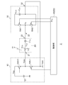
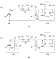
- FIG. 1 is a circuit diagram illustrating a configuration of a wireless power supply apparatus according to a first embodiment.
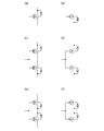
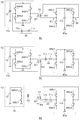
- FIGS. 3A to 3F are diagrams showing configuration examples of switches using MOSFETs.
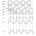
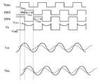
- FIG. 3 is a waveform diagram illustrating an operation of the wireless power supply apparatus of FIG. 2.
- FIG. 3 is an equivalent circuit diagram of the wireless power supply apparatus of FIG. 2.
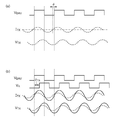
- 6A is a state where the automatic tuning assist circuit is not operated
- FIG. 6B is a waveform diagram when the automatic tuning assist circuit is operated.
- f c ⁇ f TX is a phasor diagram illustrating the quasi-resonant state by the automatic tuning assist circuit.
- FIG. 6 is a phasor diagram for explaining a quasi-resonant state by an automatic tuning auxiliary circuit when f c > f TX . It is a circuit diagram which shows the structure of the wireless electric power feeder which concerns on a 1st modification. It is a circuit diagram which shows the structure of the wireless electric power feeder which concerns on a 2nd modification. It is a circuit diagram which shows the structure of the wireless electric power feeder which concerns on a 3rd modification.
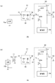
- FIGS. 13A and 13B are circuit diagrams illustrating configurations of wireless power supply apparatuses according to fourth and fifth modifications, respectively.
- FIG. 15 is an equivalent circuit diagram of the wireless power receiving apparatus of FIG. 14. It is a wave form diagram which shows operation
- FIGS. 17A and 17B are circuit diagrams showing configurations of wireless power receiving apparatuses according to first and second modifications. It is a circuit diagram which shows the structure of the wireless power receiving apparatus which concerns on a 3rd modification.
- FIGS. 19A and 19B are circuit diagrams showing configurations of wireless power receiving apparatuses according to fourth and fifth modifications, respectively. It is a circuit diagram showing an example of composition of a wireless power transmission system concerning a 1st embodiment.
- FIGS. 25A to 25C are circuit diagrams showing configurations of wireless power supply apparatuses according to second to fourth modified examples, respectively. It is a circuit diagram which shows the structure of the wireless power receiving apparatus which concerns on 2nd Embodiment. It is a wave form diagram which shows operation
- FIGS. 28A and 28B are circuit diagrams showing configurations of wireless power receiving apparatuses according to the second and third modifications, and FIGS. 28C and 28D show configuration examples of loads. It is a circuit diagram. It is a circuit diagram which shows the structure of the wireless power receiving apparatus which concerns on a 3rd modification.
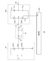
- the wireless power feeder 2 includes a power supply 10, a transmission antenna 20, an automatic tuning assist circuit 30, and a first control unit 40.
- the transmission antenna 20 includes a transmission coil L TX provided between the first end 21 and the second end 22 thereof.
- the resonance capacitor C TX is provided in series with the transmission coil L TX .
- the resonance capacitor C TX and the transmission coil L TX may be interchanged.
- the automatic tuning assist circuit 30 is coupled in series with the transmitting antenna 20.
- the power supply 10 applies an AC drive voltage V DRV having a predetermined transmission frequency f TX between both ends of the transmission antenna 20 and the automatic tuning assist circuit 30.
- the power supply 10 includes a DC power supply 12, a first high side switch SWH1, and a first low side switch SWL1.
- the DC power supply 12 generates a DC power supply voltage V DD .
- the first high-side switch SWH1 and the first low-side switch SWL1 are sequentially provided in series between the output terminal of the DC power supply 12 and the fixed voltage terminal (ground terminal).
- Automatic tuning assist circuit 30 includes a first terminal 31, second terminal 32, a first switch SW1, a second switch SW2, a first auxiliary capacitor C A1.
- the first switch SW1 and the first auxiliary capacitor CA1 are provided in series between the first terminal 31 and the second terminal 32.
- the first switch SW1 the first auxiliary capacitor C A1 may be interchanged.
- the second switch SW2 is provided between the first terminal 31 and the second terminal 32 in parallel with the first switch SW1 and the first auxiliary capacitor CA1 .
- the capacitance value of the first auxiliary capacitor C A1 is desirably sufficiently larger than that of the resonance capacitor C TX .
- the first control unit 40 a first switch SW1 and the second switch SW2, at the same frequency f TX and the driving voltage V DRV, and complementarily to the switching phase difference theta TX with respect to the driving voltage V DRV.
- the phase difference ⁇ TX may be near + 90 ° or ⁇ 90 ° (270 °). That is, a part of the first control unit 40 constitutes the automatic tuning assist circuit 30.
- the first switch SW1 and the second switch SW2 can be configured using MOSFET (Metal Oxide Semiconductor Field Effect Transistor), IGBT (Insulated Gate Bipolar Transistor), a bipolar transistor, or the like.
- FIGS. 3A and 3B are diagrams illustrating a configuration example of a switch using a MOSFET.
- FIG. 3A shows a configuration using an N-channel MOSFET
- FIG. 3B shows a configuration using a P-channel MOSFET.
- each of the switches SW1 and SW2 can be either a one-way switch or a two-way switch.
- a one-way switch it is necessary to pay attention to the switching phase. This will be described later.
- switches SW1 and SW2 are bidirectional switches that do not allow current to flow in either direction in the off state.
- FIG. 4 is a waveform diagram showing the operation of the wireless power feeder 2 of FIG. FIG. 4 shows, in order from the top, the first high-side switch SWH1, the first low-side switch SWL1, the drive voltage V DRV , the first switch SW1, the second switch SW2, the voltage V CA1 of the first auxiliary capacitor C A1 , the first terminal. 31 of the voltage V a, the resonance current I TX that flows through the transmitting antenna 20, illustrating the resonance voltage V TX across the transmission coil L TX and the resonance capacitor C TX.
- a high level indicates an on state
- a low level indicates an off state.
- the resonance current I TX and the resonance voltage V TX show waveforms in a steady state after a sufficient time has elapsed since the automatic tuning assist circuit 30 was operated.
- a rectangular wave drive voltage V DRV is generated by complementarily switching the first high-side switch SWH1 and the first low-side switch SWL1, and both ends of the transmission antenna 20 and the automatic tuning auxiliary circuit 30 are generated.
- the resonance current I TX flows to the first auxiliary capacitor C A1 during the on-time T ON1 of the first switch SW1, and flows to the ground via the second switch SW2 during the on-time T ON2 of the second switch SW2. That is, the first auxiliary capacitor C A1 is charged and discharged by the resonance current I TX , and as a result, the capacitor voltage V CA1 is generated in the first auxiliary capacitor C A1 .
- the automatic tuning assist circuit 30 applies the correction voltage V A to the second end 22 of the transmission antenna 20.
- Correction voltage V A the first switch SW1 is in the period T ON1 on, taking the first auxiliary capacitor voltage V CA1
- the second switch SW2 is in the period T ON2 on, taking the ground voltage V GND.
- the automatic tuning assist circuit 30 can be understood as a correction power source that applies the correction voltage VA to the transmission antenna 20.
- FIG. 5 is an equivalent circuit diagram of the wireless power feeder 2 of FIG.
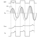
- FIG. 6A is a waveform diagram when the automatic tuning assist circuit 30 is not operated
- FIG. 6B is a waveform diagram when the automatic tuning assist circuit 30 is operated.
- the transmission antenna 20 becomes inductive when the frequency f TX of the drive voltage V DRV is higher than the resonance frequency f c (f TX > f c ), and the phase of the resonance current I TX flowing through the transmission antenna 20 is equal to that of the drive voltage V DRV . Delayed with respect to phase. On the other hand, when the frequency f TX is lower than the resonance frequency f c (f TX ⁇ f c ), it becomes capacitive, and the phase of the resonance current I TX advances with respect to the drive voltage V DRV .
- FIG. 6A shows a state where f c > f TX , and the phase of the resonance current I TX is advanced by a phase difference ⁇ with respect to the drive voltage V DRV .
- ⁇ is not 90 °
- a series resistance component exists in the resonance circuit. Since the impedance Z increases in the non-resonant state, the amplitude of the resonance current I TX decreases. In this state, a large amount of power cannot be transmitted.
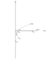
- FIG. 7 is a phasor diagram (vector diagram) for explaining a quasi-resonant state by the automatic tuning assist circuit 30 when f c ⁇ f TX .
- the phase of the drive voltage V DRV is 0 °
- the phase difference between drive voltage V DRV and current component I DRV is ⁇
- the phase difference between correction voltage V A and current component I A is also ⁇ .
- the amplitude of the correction voltage V A by optimizing the amplitude of the current component I A In other words, the combined current of the two current components I DRV and I A, i.e., the phase of the resonance current I TX, driving voltage V DRV phase ( 0 °), and a quasi-resonant state can be realized.
- FIG. 8 is a diagram illustrating the resonance current I TX in the non-resonant state and the resonance state.
- Waveform (I) shows the resonance current I TX in the non-resonant state.
- the first auxiliary capacitor C A1 is charged and discharged by the resonance current I TX .
- the first auxiliary capacitor C A1 is charged during the positive period of the resonance current I TX and discharged during the negative period.
- the capacitor voltage V CA1 increases, and if the negative period is long, the capacitor voltage V CA1 decreases.
- the capacitor voltage V CA1 increases. Then, the correction voltage V A corresponding to the increased capacitor voltage V CA1 is applied to the transmission antenna 20. Then, in the next cycle, the phase of the resonance current I TX advances from the previous cycle. When this is repeated, the phase of the resonance current ITX gradually advances while the capacitor voltage VCA1 increases every cycle, and shifts to a point (resonance point) that matches the phase of the drive voltage VDRV . If the phase of the resonance current I TX advances too much, on the contrary, the discharge current of the first auxiliary capacitor C A1 becomes larger, feedback is applied in the direction in which the capacitor voltage VC A1 decreases, and it is pulled back to the resonance point.
- the charging current and discharging current of the first auxiliary capacitor C A1 in one cycle are balanced, the capacitor voltage V CA1 is in an equilibrium state, and the pseudo resonance state is maintained.
- the correction voltage V A necessary for generating the quasi-resonant state can be automatically generated.
- the wireless power supply apparatus 2 it is possible to automatically tune without the state of the circuit to achieve a quasi-resonant state by adjusting the resonant frequency f c of the transmitting antenna 20.
- the resonance frequency changes from moment to moment depending on the positional relationship between the wireless power feeding device 2 and the wireless power receiving device 4, but the wireless power feeding device 2 can follow the change at high speed and is highly efficient. Power transmission is possible.
- variable capacitor variable capacitor
- the capacitor voltage V CA1 is automatically adjusted so as to be a negative voltage.
- the phase difference ⁇ TX may deviate from 90 ° or 270 °.
- the phase difference ⁇ TX between the current components I DRV and I A is not 90 °, but even in this case, the phase of the resonance current I TX obtained by combining them is 0 °.
- the capacitor voltage V CA1 is automatically adjusted.
- the absolute value of the capacitor voltage V CA1 can be made smaller in other words.
- FIG. 11 is a circuit diagram showing a configuration of a wireless power feeder 2b according to a second modification.
- the automatic tuning assist circuit 30b includes a charging circuit 34 and a detection resistor Rs. Detection current Rs is arranged on a path of the resonant current I TX. The detection resistor Rs, the detection voltage Vs is generated which is proportional to the resonant current I TX. Based on the detection voltage Vs, the charging circuit 34 charges the first auxiliary capacitor C A1 to a level at which a pseudo resonance state is achieved. As described above, the capacitor voltage V CA1 is automatically set to an optimum level. However, by providing the charging circuit 34, the quasi-resonant state can be obtained in a shorter time.
- FIG. 12 is a circuit diagram showing a configuration of a wireless power feeder 2c according to a third modification.
- the power source is a half-bridge circuit
- the second high side switch SWH2 and the second low side switch SWL2 are provided in series between the output terminal of the DC power supply 12 and the fixed voltage terminal (ground terminal) in order.
- the first controller 40c alternately repeats a state where the pair of the first high-side switch SWH1 and the second low-side switch SWL2 is on and a state where the pair of the second high-side switch SWH2 and the first low-side switch SWL1 is on. .
- a connection point (first output terminal) OUT1 between the first high-side switch SWH1 and the first low-side switch SWL1, and a connection point (second output terminal) OUT2 between the second high-side switch SWH2 and the second low-side switch SWL2 are connected to each other. Negative phase drive voltages V DRV and #V DRV are generated.
- the transmission antenna 20 and the automatic tuning assist circuit 30c are coupled in series between the first output terminal OUT1 and the second output terminal OUT2.
- FIGS. 13A and 13B are circuit diagrams illustrating configurations of wireless power supply apparatuses 2d and 2e according to fourth and fifth modifications, respectively.
- the first control unit 40 is omitted.
- the automatic tuning assist circuit 30d is coupled in series with the transmission antenna 20 via the first transformer T1.
- the secondary winding W2 of the first transformer T1 is provided between the first terminal 31 and the second terminal 32, and the primary winding W1 is provided in series with the transmission antenna 20.
- the power supply 10 applies a drive voltage between both ends of the transmission antenna 20 and the primary winding W1.
- the power supply 10 applies the drive voltage V DRV across the transmission antenna 20 and the automatic tuning assist circuit 30d via the second transformer T2.
- the secondary winding W2 of the second transformer T2 is provided in series with the transmission antenna 20.
- the power supply 10 applies a drive voltage V DRV across the primary winding W1 of the second transformer T2.
- the drive voltage V DRV is applied between both ends of the transmission antenna 20 and the automatic tuning assist circuit 30d through the second transformer T2. Also with this configuration, the same effect as the wireless power supply apparatus described so far can be obtained.
- the first transformer T1 may be omitted.
- the power source 10 in FIGS. 13A and 13B may be any of an H bridge circuit, a half bridge circuit, and other power sources.
- the automatic tuning assist circuit described above can also be used for a wireless power receiving apparatus.
- the wireless power receiving apparatus will be described.
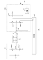
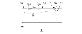
- FIG. 14 is a circuit diagram showing a configuration of the wireless power receiving apparatus 4 according to the first embodiment.
- the wireless power receiving apparatus 4 receives a power signal S1 transmitted from the above-described or completely different wireless power supply apparatus.
- a near field an electric field, a magnetic field, or an electromagnetic field
- an electromagnetic wave that is not a radio wave
- the wireless power receiving apparatus 4 includes a receiving antenna 50, an automatic tuning assist circuit 60, and a load 70 to which power is to be supplied.
- the load 70 may incorporate a rectifier circuit, a detection circuit, etc. (not shown).
- the reception antenna 50 includes a reception coil L RX and a resonance capacitor C RX provided in series between the first end 51 and the second end 52.
- the automatic tuning assist circuit 60 is configured in the same manner as the automatic tuning assist circuit 30 described above. Specifically, the third switch SW3 and the third auxiliary capacitor CA3 are provided in series between the first terminal 61 and the second terminal 62. The fourth switch SW4 is provided between the first terminal 61 and the second terminal 62 in parallel with the third switch SW3 and the third auxiliary capacitor CA3 .
- the second control unit 64 causes the third switch SW3 and the fourth switch SW4 to have the same frequency as the power signal S1 and a phase difference ⁇ RX with respect to the drive voltage (V DRV ) applied to the antenna on the transmission side.
- ⁇ RX 180 ° or 0 °.
- the automatic tuning assist circuit 60 is coupled in series with the receiving antenna 50.
- the load 70 to which power is to be supplied is connected to the third auxiliary capacitor C A3 .
- FIG. 15 is an equivalent circuit diagram of the wireless power receiving device 4 of FIG. Similar to the automatic tuning assist circuit 30 in the wireless power supply apparatus 2, the automatic tuning assist circuit 60 can be understood as a correction power source that applies the correction voltage VA to the receiving antenna 50.
- the correction voltage V A becomes the voltage V CA3 of the third auxiliary capacitor C A3 during the on time T ON3 of the third switch SW3, and becomes the ground voltage during the on time T ON4 of the fourth switch SW4.
- the third auxiliary capacitor C A3 is charged by switching the third switch SW3 and the fourth switch SW4 in a complementary manner with a phase ⁇ RX shifted by 180 ° or 0 ° with respect to the driving voltage V DRV on the wireless power feeding apparatus side. Or discharged. And by the correction voltage V A is applied to the receiving antenna 50, the phase of the resonance current I A is consistent with the phase of the transmission side of the driving voltage V DRV, quasi-resonant state can be realized.
- the resonance state can be automatically realized without adjusting the capacitance value of the resonance capacitor C RX .
- FIGS. 17A and 17B are circuit diagrams showing configurations of wireless power receiving apparatuses according to first and second modifications.
- the load 70a is provided in series with the receiving antenna 50 and the automatic tuning assist circuit 60. Specifically, the load 70 a is connected to the first end 51 of the receiving antenna 50.
- 17B includes a third transformer T3, and the receiving antenna 50 and the load 70b are insulated by the third transformer T3.
- the primary winding W1 of the third transformer T3 is provided in series with the receiving antenna 50, and a load 70b is connected to the secondary winding W2.
- the Q value of the receiving antenna 50 is not lowered by the load 70, so that a large amount of power can be taken out even when the impedance of the load 70 is high.
- the impedance of the load 70 is too low, there is a problem that the operation of the automatic tuning assist circuit 60 is hindered.
- the position where the load is arranged may be determined in consideration of the power to be transmitted, the impedance of the load, and the like.
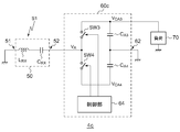
- FIG. 18 is a circuit diagram showing a configuration of a wireless power receiving device 4c according to the third modification.
- Automatic tuning assist circuit 60c further includes a first terminal 61 and the fourth auxiliary capacitor C A4 provided in the fourth switch SW4 series between the second terminal 62.
- the position of the load 70 is not limited.
- the correction voltage V A is equal to the capacitor voltage V CA3 at the on time T ON3 of the third switch SW3, and is equal to the capacitor voltage V CA4 at the on time T ON4 of the fourth switch SW4.
- the capacitor voltages V CA1 and V CA2 can be optimized so that the pseudo resonance state is obtained in the respective states of f TX > f c and f TX ⁇ f c .
- the third switch SW3 and the fourth switch SW4 may be configured by either a unidirectional switch or a bidirectional switch. In the case of a unidirectional switch, it is necessary to switch the third switch SW3 and the fourth switch SW4 at a phase where no current flows through each reverse conducting element.
- FIGS. 19A and 19B are circuit diagrams showing configurations of wireless power receiving apparatuses according to fourth and fifth modifications, respectively.
- the second control unit 64 is omitted.
- the automatic tuning assist circuit 60d is coupled in series with the receiving antenna 50 via the fourth transformer T4.
- the secondary winding W2 of the fourth transformer T4 is provided between the first terminal 61 and the second terminal 62, and the primary winding W1 is provided in series with the receiving antenna 50.
- the load 70 is coupled to the receiving antenna 50 and the automatic tuning assist circuit 60d via the fifth transformer T5.
- the primary winding W1 of the fifth transformer T5 is connected in series with the receiving antenna 50.
- the load 70 is connected to both ends of the secondary winding W2 of the fifth transformer T5.
- the fourth transformer T4 may be omitted.
- the load 70 may be coupled to the third auxiliary capacitor C A3 .
- the load 70 may be coupled via the third auxiliary capacitor CA3 and the fifth transformer T5.
- a wireless power transmission system can be realized by combining the above-described wireless power feeding apparatus and wireless power receiving apparatus.
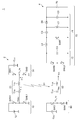
- FIG. 20 is a circuit diagram showing a configuration example of the wireless power transmission system according to the first embodiment.
- the wireless power transmission system 1 includes a wireless power feeder 2 and a wireless power receiver 4.
- the load 70 includes a rectifier circuit 72 and a switching regulator 74 in addition to the load circuit 76.
- the rectifier circuit 72 is a synchronous detection circuit, and includes a smoothing capacitor C3, a third high side switch SWH3, and a third low side switch SWL3.
- the switching regulator 74 is a step-up / step-down converter and is controlled so that the maximum power can be supplied to the load circuit 76. Since the configuration and operation of the switching regulator 74 are known, the description thereof is omitted here.
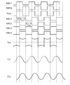
- FIG. 21 is a waveform diagram showing an operation of the wireless power transmission system 1 of FIG.
- the third switch SW3 is driven with a phase delayed by 90 ° with respect to the first switch SW1.
- the quasi-resonant state is also established in the wireless power receiving device 4.
- the third high-side switch SWH3 and the third low-side switch SWL3 of the rectifier circuit 72 are driven with a phase delayed by 90 ° with respect to the third switch SW3 and the fourth switch SW4. As a result, a DC voltage is generated in the smoothing capacitor C3. This DC voltage is converted to an optimum voltage level for the load circuit 76 by the switching regulator 74.
- the above is the operation of the wireless power transmission system 1. As described above, according to the wireless power transmission system 1, it is possible to transmit the maximum power to the load 70 by providing the automatic tuning assist circuit in each of the wireless power feeding device 2 and the wireless power receiving device 4.
- an automatic tuning assist circuit may be provided only in the wireless power feeding apparatus 2, and the wireless power receiving apparatus may adjust the resonance capacitor C RX as in the related art.
- an automatic tuning assist circuit may be provided only in the wireless power receiving device 4, and the wireless power feeding device 2 may adjust the resonance capacitor C TX as in the related art.
- an automatic tuning assist circuit is provided only in the wireless power feeding apparatus 2, and the wireless power receiving apparatus 4 may not have any adjustment mechanism.
- an automatic tuning assist circuit may be provided only in the wireless power receiving device 4, and the wireless power feeding device 2 may not have any adjustment mechanism.
- the single automatic tuning assist circuit is tuned so that impedance matching between the power supply 10 and the load 70 can be obtained, and high-efficiency power transmission is possible.
- the optimum value of the switching phase ⁇ TX ( ⁇ RX ) of the automatic tuning assist circuit deviates from 90 ° or 270 ° (180 ° or 0 °).
- the wireless power supply apparatus 6 it is possible to automatically tune without the state of the circuit to achieve a quasi-resonant state by adjusting the resonant frequency f c of the transmitting antenna 20.
- the resonance frequency changes from moment to moment depending on the positional relationship between the wireless power feeding device and the wireless power receiving device.
- the change can be followed at high speed, and highly efficient power transmission. Is possible.
- variable capacitor variable capacitor
- the phase difference ⁇ TX need not be 90 °, and may be 270 ° ( ⁇ 90 °).
- the capacitor voltage V CA1 is automatically adjusted so as to have a reverse polarity.
- phase difference ⁇ TX may be out of 90 ° or 270 °.
- the first control unit 40 drives the plurality of switches constituting the automatic tuning assist circuit 80 at the same frequency f TX as the drive voltage V DRV has been described, but the present invention is not limited thereto. Not.
- the first control unit 40 can also realize a pseudo resonance state by switching the switch at a frequency that is an odd multiple of the drive voltage V DRV or a frequency that is an odd multiple of an odd number.
- FIGS. 25A to 25C are circuit diagrams showing configurations of wireless power supply apparatuses 6b to 6d according to second to fourth modifications, respectively.
- the first control unit 40 is omitted.
- the automatic tuning assist circuit 80a is coupled in series with the transmission antenna 20 via the sixth transformer T6.
- the primary winding W1 of the sixth transformer T6 is provided in series with the transmitting antenna 20, and the secondary winding W2 is connected to the first terminal 61 and the second terminal 62 of the automatic tuning assist circuit 80a.
- the power supply 10c applies a drive voltage between both ends of the transmission antenna 20 and the primary winding W1 of the sixth transformer T6.
- the power source 10c is coupled to the transmission antenna 20 and the automatic tuning assist circuit 80a via the seventh transformer T7.
- the power source 10c applies a driving voltage to both ends of the primary winding W1 of the seventh transformer T7.
- the transmitting antenna 20 and the automatic tuning assist circuit 80a are provided in series with the secondary winding W2.
- the power supply 10 having a half bridge configuration is coupled to the transmission antenna 20 and the automatic tuning assist circuit 80a via the seventh transformer T7.
- a DC blocking capacitor C3 is provided between the output terminal of the power supply 10 and the first winding W1 of the seventh transformer T7.
- both the power source and the automatic tuning assist circuit may be coupled to the transmitting antenna by a transformer.
- the wireless power receiving device 8 includes a receiving antenna 50, an automatic tuning assist circuit 90, and a load 70 to which power is to be supplied.
- the load 70 may incorporate a rectifier circuit, a detection circuit, etc. (not shown).
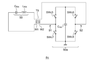
- the fifth switch SWc5 and the sixth switch SWc6 are provided in series between the first terminal 91 and the second terminal 92.
- the seventh switch SWc7 and the eighth switch SWc8 are provided in series between the first terminal 91 and the second terminal 92 in order and in parallel with the fifth switch SWc5 and the sixth switch SWc6.
- the capacitance value of the second auxiliary capacitor C A6 is desirably sufficiently larger than that of the resonance capacitor C RX .
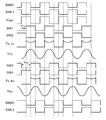
- FIG. 27 is a waveform diagram showing an operation of the wireless power receiving device 8 of FIG. Figure 27 is from the top, the fifth switch SWc5 ⁇ eighth switch SWc8, the correction voltage V A, the resonance current I RX flowing into the reception antenna 50, the resonance voltage V RX across the receiving coil L RX and the resonance capacitor C RX Indicates.
- a high level indicates an on state
- a low level indicates an off state.
- the resonance state can be automatically realized without adjusting the capacitance value of the resonance capacitor C RX .
- the second control unit 64 drives a plurality of switches constituting the automatic tuning assist circuit 30 at the same frequency as the power signal S1 has been described, but the present invention is not limited thereto.
- the second control unit 64 can also realize a pseudo resonance state by switching the switch at a frequency that is an odd multiple of the power signal S1 or a frequency that is an odd multiple of the odd number.
- one end of the load 70 is grounded to be a reference potential, but instead of grounding one end of the load 70, one end of the second auxiliary capacitor CA6 of the automatic tuning auxiliary circuit 90, that is, the connection point N3 or N4. One may be grounded.
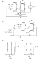
- FIGS. 28A and 28B are circuit diagrams showing the configurations of the wireless power receiving apparatuses according to the second and third modifications.
- FIGS. 28C and 28D are circuit diagrams showing configuration examples of loads.
- the load 70c in FIG. 28C includes a diode rectifier circuit 72c and a load circuit 76.
- the load 70d in FIG. 28D includes a synchronous detection circuit 72d and a load circuit 76.
- the load circuit may further include a switching regulator 74 as shown in FIG.
- the position where the load is arranged may be determined in consideration of the power to be transmitted, the impedance of the load, and the like.
- the fifth switch SWc5 to the eighth switch SWc8 can be either bidirectional switches or unidirectional switches. As described above, when using one-way switches, it is necessary to pay attention to the phase of the switching.
- a wireless power transmission system can be realized by combining the wireless power feeder 6 and the wireless power receiver 8 described in the second embodiment.
- an automatic tuning assist circuit may be provided only in the wireless power feeding device 6, and the wireless power receiving device may adjust the resonance capacitor C RX as in the related art.
- an automatic tuning assist circuit may be provided only in the wireless power receiving device 8, and the wireless power feeding device 6 may adjust the resonance capacitor CTX as in the related art.
- an automatic tuning assist circuit is provided only in the wireless power feeding device 6, and the wireless power receiving device 8 may not have any adjustment mechanism.
- an automatic tuning assist circuit may be provided only in the wireless power receiving device 8, and the wireless power feeding device 6 may not have any adjustment mechanism.
- the single automatic tuning assist circuit is tuned so that impedance matching between the power supply 10 and the load 70 can be obtained, and high-efficiency power transmission is possible.
- the optimum value of the switching phase ⁇ TX ( ⁇ RX ) of the automatic tuning assist circuit deviates from 90 ° or 270 ° (180 ° or 0 °).
- the wireless power feeder 2 according to the first embodiment may be combined with the wireless power receiver 8 according to the second embodiment, or the wireless power receiver 4 may be combined with the wireless power feeder 6.
- the resonance capacitor C TX may be omitted.
- the resonance capacitor CRX may be omitted.
- the wireless power supply device 6 changes at least one of the frequency f TX and the phase of the drive voltage V DRV according to a predetermined rule (encryption code), and encrypts the power signal S1.
- the wireless power receiving apparatus 8 that knows the encryption code controls the switching frequency and phase of the automatic tuning assist circuit 90 based on the encryption code. As a result, even when the power signal S1 is encrypted, it can be decrypted and supplied with power. Since the wireless power receiving apparatus that does not know the encryption code cannot properly control the switch of the automatic tuning assist circuit 90, it cannot receive power. In wireless power transmission, theft by a malicious user can be a problem, but this problem can be solved by using an automatic tuning assist circuit. Alternatively, when a single wireless power supply device 6 supplies power to a plurality of wireless power reception devices 8, the power supply amount for each terminal can be controlled by using an automatic tuning assist circuit.
- the application of the automatic tuning assist circuit 30 is not limited to wireless power transmission, and can be used for various applications that require tuning.
- SYMBOLS 1 ... Wireless power transmission system, 2 ... Wireless power feeder, 4 ... Wireless power receiver, 6 ... Wireless power feeder, 8 ... Wireless power receiver, 10 ... Power supply, 12 ... DC power supply, SWH1 ... First high side switch, SWL1 ... First 1 low side switch, SWH2 ... second high side switch, SWL2 ... second low side switch, 20 ... transmission antenna, 22 ... first end, 24 ... second end, L TX ... transmission coil, C TX ... resonance capacitor, 30 ... automatic tuning auxiliary circuit, 31 ... first terminal, 32 ... second terminal, 34 ... charging circuit, C A1 ... first auxiliary capacitor, C A2 ... second auxiliary capacitor, C A3 ...
- Automatic tuning Auxiliary circuit 81 ... first terminal, 82 ... second terminal, SWc1 ... first switch, SWc2 ... second switch, SWc3 ... third switch, SWc4 ... fourth switch, C A5 ... first auxiliary capacitor, 90 ... automatic Tuning auxiliary circuit 91 ... first terminal 92 ... second terminal SWc5 ... fifth switch SWc6 ... sixth switch SWc7 ... seventh switch , SWc8 ... eighth switch, C A6 ... second auxiliary capacitor, 94 ... second control unit.
- the present invention can be used for wireless power feeding technology.
Landscapes
- Engineering & Computer Science (AREA)
- Computer Networks & Wireless Communication (AREA)
- Power Engineering (AREA)
- Signal Processing (AREA)
- Current-Collector Devices For Electrically Propelled Vehicles (AREA)
- Charge And Discharge Circuits For Batteries Or The Like (AREA)
- Transmitters (AREA)
- Rectifiers (AREA)
Abstract
Description
数m以上の比較的長い距離に給電する場合、電波受信型が利用される。電波受信型では、中波~マイクロ波の帯域で数W以下の電力を伝送することができるが、電力の利用効率は低い。数m程度の中距離を、比較的高い効率で給電する手法として、電場・磁場共鳴型が着目されている(非特許文献1参照)。
この場合、第1補助キャパシタに加えて、第2補助キャパシタが、共振電流と駆動電圧が同位相となるように充電もしくは放電されることになり、擬似的な共振状態を実現できる。
第2制御部は、ワイヤレス給電装置において送信アンテナに印加される駆動電圧に対して、所定の位相差で第3スイッチおよび第4スイッチを駆動してもよい。
この場合、第3補助キャパシタに加えて、第4補助キャパシタが、共振電流と駆動電圧が同位相となるように充電もしくは放電され、擬似的な共振状態を実現できる。
ある態様のワイヤレス受電装置は、その1次巻線が受信アンテナと直列に設けられたトランスをさらに備えてもよい。電力を供給すべき負荷は、トランスの2次巻線に接続されてもよい。
自動チューニング補助回路を設けることで、擬似的な共振状態を実現でき、共振用キャパシタの容量値の調節などを行わなくても、送信アンテナを駆動電圧に対して自動的にチューニングすることができる。
自動チューニング補助回路を設けることで、擬似的な共振状態を実現でき、共振用キャパシタの容量値の調節などを行わなくても、受信アンテナを電力信号に対して自動的にチューニングすることができる。
同様に、「部材Cが、部材Aと部材Bの間に設けられた状態」とは、部材Aと部材C、あるいは部材Bと部材Cが直接的に接続される場合のほか、それらの電気的な接続状態に実質的な影響を及ぼさない、あるいはそれらの結合により奏される機能や効果を損なわせない、その他の部材を介して間接的に接続される場合も含む。
(ワイヤレス給電装置)
図2は、第1の実施の形態に係るワイヤレス給電装置2の構成を示す回路図である。ワイヤレス給電装置2は、ワイヤレス受電装置(不図示)に対して電力信号S1を送出する。電力信号S1は、電波になっていない電磁波の近傍界(電界、磁界、あるいは電磁界)が利用される。
はじめに図6(a)を参照し、自動チューニング補助回路30を動作させない状態、すなわち第1スイッチSW1をオフで固定し、第2スイッチSW2をオンで固定した状態について説明する。これは、補正電圧VAが接地電圧VGNDに固定される状態を示す。
送信アンテナ20のインピーダンスZは式(1)で与えられ、その共振周波数fcは式(2)で与えられる。なお、ここでは抵抗成分を無視しているが、実際の回路には直列抵抗が寄与することは言うまでもない。
Z=jωLTX+1/(jωCTX) …(1)
fC=1/(2π√(LTX・CTX)) …(2)
駆動電圧VDRVの位相は0°、補正電圧VAの位相はθTX=90°である。fc<fTXにおいて、電流の位相は、電圧に対して位相差φ遅れる。したがって駆動電圧VDRVと電流成分IDRVの位相差はφであり、補正電圧VAと電流成分IAの位相差もφである。
図8は、非共振状態および共振状態における共振電流ITXを示す図である。波形(I)は、非共振状態における共振電流ITXを示す。スイッチSW1がオンの期間TON1において、第1補助キャパシタCA1は、共振電流ITXによって充放電される。具体的には、第1補助キャパシタCA1は、共振電流ITXが正の期間に充電され、負の期間に放電される。その結果、正の期間が長ければキャパシタ電圧VCA1は増大し、負の期間が長ければキャパシタ電圧VCA1は低下する。
このようにワイヤレス給電装置2によれば、送信アンテナ20の共振周波数fcを調節することなく、疑似共振状態を実現するように回路の状態を自動的にチューニングすることができる。ワイヤレス送電では、ワイヤレス給電装置2とワイヤレス受電装置4の位置関係によって、共振周波数が時々刻々と変化するが、ワイヤレス給電装置2によれば、その変化に高速に追従することができ、高効率な電力伝送が可能となる。
位相差θTXは、90°もしくは270°から外れていてもよい。この場合、図7に示すベクトル図において、電流成分IDRVとIAの位相差θTXが90°ではなくなるが、この場合でも、それらを合成した共振電流ITXの位相が0°となるように、キャパシタ電圧VCA1が自動的に調節される。ただし、位相差θTXが90°もしくは270°に近いほど、電流成分IAの振幅、言い換えればキャパシタ電圧VCA1の絶対値が小さくできるという利点がある。
これまでは電源がハーフブリッジ回路の場合を説明したが、図12の電源10cはHブリッジ回路で構成される。第2ハイサイドスイッチSWH2および第2ローサイドスイッチSWL2は、直流電源12の出力端子と固定電圧端子(接地端子)の間に順に直列に設けられる。
第1ハイサイドスイッチSWH1と第1ローサイドスイッチSWL1の接続点(第1出力端子)OUT1と、第2ハイサイドスイッチSWH2と第2ローサイドスイッチSWL2の接続点(第2出力端子)OUT2には、互いに逆相の駆動電圧VDRV、#VDRVが発生する。送信アンテナ20および自動チューニング補助回路30cは、第1出力端子OUT1と第2出力端子OUT2の間に直列にカップリングされる。
図13(a)のワイヤレス給電装置2dにおいて、自動チューニング補助回路30dは、第1トランスT1を介して送信アンテナ20と直列にカップリングされる。具体的には、第1トランスT1の2次巻線W2は第1端子31と第2端子32の間に設けられ、その1次巻線W1は、送信アンテナ20と直列に設けられる。電源10は、送信アンテナ20と1次巻線W1の両端間に駆動電圧を印加する。
上述した自動チューニング補助回路は、ワイヤレス受電装置にも利用することができる。以下では、ワイヤレス受電装置について説明する。
このように図14のワイヤレス受電装置4によれば、共振用キャパシタCRXの容量値を調節することなく、自動的に共振状態を実現することができる。
図19(a)のワイヤレス受電装置4dにおいて、自動チューニング補助回路60dは、第4トランスT4を介して受信アンテナ50と直列にカップリングされる。具体的には、第4トランスT4の2次巻線W2は第1端子61と第2端子62の間に設けられ、その1次巻線W1は、受信アンテナ50と直列に設けられる。
上述のワイヤレス給電装置とワイヤレス受電装置を組み合わせることにより、ワイヤレス送電システムを実現できる。
ワイヤレス給電装置2にのみ自動チューニング補助回路を設け、ワイヤレス受電装置は、従来のように共振用キャパシタCRXの調節を行ってもよい。
反対にワイヤレス受電装置4にのみ自動チューニング補助回路を設け、ワイヤレス給電装置2は、従来のように共振用キャパシタCTXの調節を行ってもよい。
これらの場合、単一の自動チューニング補助回路によって、電源10と負荷70の間のインピーダンスマッチングがとれるようにチューニングされ、高効率な電力伝送が可能となる。この場合に、自動チューニング補助回路のスイッチングの位相θTX(θRX)の最適値は90°もしくは270°(180°もしくは0°)から外れることに留意すべきである。
あるいは、単一のワイヤレス給電装置2が複数のワイヤレス受電装置4に給電する際に、自動チューニング補助回路を利用することにより端末毎の給電量を制御できる。
第1の実施の形態では、2つのスイッチSW1、SW2を含む自動チューニング補助回路を説明した。第2の実施の形態における自動チューニング補助回路は、4つのスイッチを含んで構成される。自動チューニング補助回路80を除くブロックの構成については、第1の実施の形態と同様である。また、第1の実施の形態で説明したさまざまな変形例は、第2の実施の形態においても有効である。
図22は、第2の実施の形態に係るワイヤレス給電装置2の構成を示す回路図である。ワイヤレス給電装置2は、ワイヤレス受電装置(不図示)に対して電力信号S1を送出する。電力信号S1は、電波になっていない電磁波の近傍界(電界、磁界、あるいは電磁界)が利用される。
このようにワイヤレス給電装置6によれば、送信アンテナ20の共振周波数fcを調節することなく、疑似共振状態を実現するように回路の状態を自動的にチューニングすることができる。ワイヤレス送電では、ワイヤレス給電装置とワイヤレス受電装置の位置関係によって、共振周波数が時々刻々と変化するが、ワイヤレス給電装置6によれば、その変化に高速に追従することができ、高効率な電力伝送が可能となる。
fc<fTXのときにθTX=90°
fc>fTXのときにθTX=270°
とすることが望ましい。
上述した第2の実施の形態に係る自動チューニング補助回路は、ワイヤレス受電装置にも利用することができる。以下では、ワイヤレス受電装置について説明する。
このように図26のワイヤレス受電装置8によれば、共振用キャパシタCRXの容量値を調節することなく、自動的に共振状態を実現することができる。
図28(a)に示す第1の変形例に係るワイヤレス受電装置8aでは、自動チューニング補助回路90aの接続点N4が接地される。負荷70aは、第2補助キャパシタCA6と並列に設けられる。すなわち負荷70aには、第2補助キャパシタCA6に生ずるキャパシタ電圧VCA6が供給される。
第2の実施の形態で説明したワイヤレス給電装置6とワイヤレス受電装置8を組み合わせることにより、ワイヤレス送電システムを実現できる。
ワイヤレス給電装置6にのみ自動チューニング補助回路を設け、ワイヤレス受電装置は、従来のように共振用キャパシタCRXの調節を行ってもよい。反対にワイヤレス受電装置8にのみ自動チューニング補助回路を設け、ワイヤレス給電装置6は、従来のように共振用キャパシタCTXの調節を行ってもよい。
これらの場合、単一の自動チューニング補助回路によって、電源10と負荷70の間のインピーダンスマッチングがとれるようにチューニングされ、高効率な電力伝送が可能となる。この場合に、自動チューニング補助回路のスイッチングの位相θTX(θRX)の最適値は90°もしくは270°(180°もしくは0°)から外れることに留意すべきである。
あるいは、単一のワイヤレス給電装置6が複数のワイヤレス受電装置8に給電する際に、自動チューニング補助回路を利用することにより端末毎の給電量を制御できる。
Claims (32)
- ワイヤレス受電装置に対して、電界、磁界、電磁界のいずれかを含む電力信号を送信するワイヤレス給電装置であって、
送信コイルを含む送信アンテナと、
前記送信アンテナとカップリングされる自動チューニング補助回路と、
前記送信アンテナおよび前記自動チューニング補助回路の両端間に交流の駆動電圧を印加する電源と、
を備え、
前記自動チューニング補助回路は、
第1端子と、
第2端子と、
N個(Nは自然数)の補助キャパシタと、
それぞれが、前記第1端子、前記第2端子、前記N個の補助キャパシタの端子のうち2つの間に設けられた複数のスイッチと、
前記複数のスイッチそれぞれを、前記駆動電圧と同期してスイッチングする第1制御部と、
を備えることを特徴とするワイヤレス給電装置。 - 前記第1制御部は、前記複数のスイッチそれぞれを、前記駆動電圧と同じ周波数、その奇数倍または奇数分の1倍の周波数でスイッチングすることを特徴とする請求項1に記載のワイヤレス給電装置。
- 前記自動チューニング補助回路は、
前記第1端子と前記第2端子の間に直列に設けられた、第1スイッチおよび第1補助キャパシタと、
前記第1端子と前記第2端子の間に、前記第1スイッチおよび前記第1補助キャパシタに対して並列に設けられた第2スイッチと、
を含むことを特徴とする請求項1または2に記載のワイヤレス給電装置。 - 前記第1制御部は、前記第1スイッチおよび前記第2スイッチを、前記駆動電圧と同じ周波数で、かつ駆動電圧に対してある位相差でスイッチングすることを特徴とする請求項3に記載のワイヤレス給電装置。
- 前記自動チューニング補助回路は、
前記第1端子と前記第2端子の間に、前記第2スイッチと直列に設けられた第2補助キャパシタをさらに含むことを特徴とする請求項3または4に記載のワイヤレス給電装置。 - 前記第1スイッチ、前記第2スイッチは、片方向スイッチで構成され、
前記第1制御部は、前記第1スイッチおよび前記第2スイッチを、それぞれの逆導通素子に電流が流れない位相でスイッチングすることを特徴とする請求項3から5のいずれかに記載のワイヤレス給電装置。 - 前記第1スイッチ、前記第2スイッチは、双方向スイッチで構成されることを特徴とする請求項3から6のいずれかに記載のワイヤレス給電装置。
- 前記自動チューニング補助回路は、トランスを介して前記送信アンテナと直列にカップリングされることを特徴とする請求項1から7のいずれかに記載のワイヤレス給電装置。
- 前記電源は、
直流電源と、
前記直流電源の出力端子と固定電圧端子の間に順に直列に設けられた第1ハイサイドスイッチおよび第1ローサイドスイッチと、
を含み、
前記送信アンテナおよび前記自動チューニング補助回路は、前記第1ハイサイドスイッチおよび前記第1ローサイドスイッチの接続点と前記固定電圧端子との間に直列にカップリングされることを特徴とする請求項1から8のいずれかに記載のワイヤレス給電装置。 - 前記電源は、
直流電源と、
前記直流電源の出力端子と固定電圧端子の間に順に直列に設けられた第1ハイサイドスイッチおよび第1ローサイドスイッチと、
前記直流電源の出力端子と前記固定電圧端子の間に順に直列に設けられた第2ハイサイドスイッチおよび第2ローサイドスイッチと、
を含み、
前記送信アンテナおよび前記自動チューニング補助回路は、前記第1ハイサイドスイッチおよび前記第1ローサイドスイッチの接続点と、前記第2ハイサイドスイッチおよび前記第2ローサイドスイッチの接続点との間に直列にカップリングされることを特徴とする請求項1から8のいずれかに記載のワイヤレス給電装置。 - 前記送信アンテナは、
前記送信コイルと直列に設けられた共振用キャパシタを含むことを特徴とする請求項1から10のいずれかに記載のワイヤレス給電装置。 - 前記電源は、前記送信アンテナおよび前記自動チューニング補助回路の両端間に、トランスを介して交流の駆動電圧を印加することを特徴とする請求項1から11のいずれかに記載のワイヤレス給電装置。
- 請求項1から12のいずれかに記載のワイヤレス給電装置と、
前記ワイヤレス給電装置からの電力信号を受信するワイヤレス受電装置と、
を備えることを特徴とするワイヤレス給電システム。 - ワイヤレス給電装置から送信される電界、磁界、電磁界のいずれかを含む電力信号を受信するワイヤレス受電装置であって、
受信コイルを含む受信アンテナと、
前記受信アンテナとカップリングされる自動チューニング補助回路と、
を備え、
前記自動チューニング補助回路は、
第1端子と、
第2端子と、
N個(Nは自然数)の補助キャパシタと、
それぞれが、前記第1端子、前記第2端子、前記N個の補助キャパシタの端子のうち2つの間に設けられた複数のスイッチと、
前記複数のスイッチそれぞれをスイッチングする第2制御部と、
を備えることを特徴とするワイヤレス受電装置。 - 前記第2制御部は、前記複数のスイッチそれぞれを、前記電力信号と同じ周波数、その奇数倍または奇数分の1倍の周波数でスイッチングすることを特徴とする請求項14に記載のワイヤレス受電装置。
- 前記自動チューニング補助回路は、
前記第1端子と前記第2端子の間に直列に設けられた、第3スイッチおよび第3補助キャパシタと、
前記第1端子と前記第2端子の間に、前記第3スイッチおよび前記第3補助キャパシタに対して並列に設けられた第4スイッチと、
を含むことを特徴とする請求項14または15に記載のワイヤレス受電装置。 - 前記第2制御部は、前記第3スイッチおよび前記第4スイッチを前記電力信号と同じ周波数でスイッチングすることを特徴とする請求項16に記載のワイヤレス受電装置。
- 前記第2制御部は、前記ワイヤレス給電装置において送信アンテナに印加される駆動電圧に対して、所定の位相差で前記第3スイッチおよび前記第4スイッチを駆動することを特徴とする請求項16に記載のワイヤレス受電装置。
- 前記自動チューニング補助回路は、
前記第1端子と前記第2端子の間に、前記第4スイッチと直列に設けられた第4補助キャパシタをさらに備えることを特徴とする請求項16から18のいずれかに記載のワイヤレス受電装置。 - 前記第3スイッチ、前記第4スイッチは、片方向スイッチで構成され、
前記第2制御部は、前記第3スイッチおよび前記第4スイッチを、それぞれの逆導通素子に電流が流れない位相でスイッチングすることを特徴とする請求項16から19のいずれかに記載のワイヤレス受電装置。 - 前記第3スイッチ、前記第4スイッチは、双方向スイッチで構成されることを特徴とする請求項16から19のいずれかに記載のワイヤレス受電装置。
- 電力を供給すべき負荷は、前記第3補助キャパシタに接続されることを特徴とする請求項16から21のいずれかに記載のワイヤレス受電装置。
- 電力を供給すべき負荷は、前記受信アンテナの第1端に接続されることを特徴とする請求項14から22のいずれかに記載のワイヤレス受電装置。
- その1次巻線が前記受信アンテナと直列に設けられたトランスをさらに備え、
電力を供給すべき負荷は、前記トランスの2次巻線に接続されることを特徴とする請求項14から23のいずれかに記載のワイヤレス受電装置。 - 前記自動チューニング補助回路は、トランスを介して前記受信アンテナと直列にカップリングされることを特徴とする請求項14から24のいずれかに記載のワイヤレス受電装置。
- 前記受信アンテナは、前記受信コイルと直列に設けられた共振用キャパシタを含むことを特徴とする請求項14から25のいずれかに記載のワイヤレス受電装置。
- 電界、磁界、電磁界のいずれかを含む電力信号を送信するワイヤレス給電装置と、
前記電力信号を受信する請求項14から26のいずれかに記載のワイヤレス受電装置と、
を備えることを特徴とするワイヤレス給電システム。 - 請求項1から12のいずれかに記載のワイヤレス給電装置と、
前記ワイヤレス給電装置からの前記電力信号を受信する請求項14から26のいずれかに記載のワイヤレス受電装置と、
を備えることを特徴とするワイヤレス給電システム。 - ワイヤレス受電装置に対して、送信コイルから電界、磁界、電磁界のいずれかを含む電力信号を送信するワイヤレス給電装置に使用され、前記送信コイルとカップリングされる自動チューニング補助回路であって、
少なくともひとつの補助キャパシタと、
前記送信コイルに流れる共振電流によって前記少なくともひとつの補助キャパシタそれぞれを充電および放電するために設けられた複数のスイッチと、
前記複数のスイッチをスイッチングすることにより、前記少なくともひとつの補助キャパシタそれぞれの両端間にキャパシタ電圧を発生させるとともに、前記少なくともひとつの補助キャパシタそれぞれのキャパシタ電圧に応じた補正電圧を、前記送信コイルに印加せしめる第1制御部と、
を備えることを特徴とする自動チューニング補助回路。 - ワイヤレス受電装置に対して、電界、磁界、電磁界のいずれかを含む電力信号を送信するワイヤレス給電装置であって、
送信コイルを含む送信アンテナと、
前記送信アンテナとカップリングされる請求項29に記載の自動チューニング補助回路と、
前記送信アンテナおよび前記自動チューニング補助回路の両端間に交流の駆動電圧を印加する電源と、
を備えることを特徴とするワイヤレス給電装置。 - ワイヤレス給電装置から送信される電界、磁界、電磁界のいずれかを含む電力信号を受信コイルにより受信するワイヤレス受電装置に使用され、前記受信コイルとカップリングされる自動チューニング補助回路であって、
少なくともひとつの補助キャパシタと、
前記受信コイルに流れる共振電流によって前記少なくともひとつの補助キャパシタそれぞれを充電および放電するために設けられた複数のスイッチと、
前記複数のスイッチをスイッチングすることにより、前記少なくともひとつの補助キャパシタそれぞれの両端間にキャパシタ電圧を発生させるとともに、前記少なくともひとつの補助キャパシタそれぞれのキャパシタ電圧に応じた補正電圧を、前記受信コイルに印加せしめる第2制御部と、
を備えることを特徴とする自動チューニング補助回路。 - ワイヤレス給電装置から送信される電界、磁界、電磁界のいずれかを含む電力信号を受信するワイヤレス受電装置であって、
受信コイルを含む受信アンテナと、
前記受信アンテナとカップリングされる請求項31に記載の自動チューニング補助回路と、
を備えることを特徴とするワイヤレス受電装置。
Priority Applications (4)
| Application Number | Priority Date | Filing Date | Title |
|---|---|---|---|
| JP2013517842A JP5860458B2 (ja) | 2011-06-02 | 2012-05-16 | ワイヤレス受電装置、ワイヤレス給電装置およびワイヤレス給電システム、自動チューニング補助回路 |
| KR1020137035120A KR20140037894A (ko) | 2011-06-02 | 2012-05-16 | 무선 수전 장치, 무선 급전 장치 및 무선 급전 시스템, 자동 튜닝 보조 회로 |
| US14/093,241 US9633782B2 (en) | 2011-06-02 | 2013-11-29 | Wireless power transmitter |
| US15/420,504 US10243408B2 (en) | 2011-06-02 | 2017-01-31 | Wireless power receiver |
Applications Claiming Priority (4)
| Application Number | Priority Date | Filing Date | Title |
|---|---|---|---|
| JP2011124443 | 2011-06-02 | ||
| JP2011-124443 | 2011-06-02 | ||
| JP2011-128661 | 2011-06-08 | ||
| JP2011128661 | 2011-06-08 |
Related Child Applications (1)
| Application Number | Title | Priority Date | Filing Date |
|---|---|---|---|
| US14/093,241 Continuation US9633782B2 (en) | 2011-06-02 | 2013-11-29 | Wireless power transmitter |
Publications (1)
| Publication Number | Publication Date |
|---|---|
| WO2012164845A1 true WO2012164845A1 (ja) | 2012-12-06 |
Family
ID=47258723
Family Applications (2)
| Application Number | Title | Priority Date | Filing Date |
|---|---|---|---|
| PCT/JP2012/003191 Ceased WO2012164846A1 (ja) | 2011-06-02 | 2012-05-16 | ワイヤレス受電装置、ワイヤレス給電装置およびワイヤレス給電システム、自動チューニング補助回路 |
| PCT/JP2012/003190 Ceased WO2012164845A1 (ja) | 2011-06-02 | 2012-05-16 | ワイヤレス受電装置、ワイヤレス給電装置およびワイヤレス給電システム、自動チューニング補助回路 |
Family Applications Before (1)
| Application Number | Title | Priority Date | Filing Date |
|---|---|---|---|
| PCT/JP2012/003191 Ceased WO2012164846A1 (ja) | 2011-06-02 | 2012-05-16 | ワイヤレス受電装置、ワイヤレス給電装置およびワイヤレス給電システム、自動チューニング補助回路 |
Country Status (5)
| Country | Link |
|---|---|
| US (3) | US9552921B2 (ja) |
| JP (2) | JP5860458B2 (ja) |
| KR (2) | KR20140037895A (ja) |
| TW (2) | TWI509931B (ja) |
| WO (2) | WO2012164846A1 (ja) |
Cited By (5)
| Publication number | Priority date | Publication date | Assignee | Title |
|---|---|---|---|---|
| WO2013132755A1 (ja) * | 2012-03-06 | 2013-09-12 | 株式会社アドバンテスト | ワイヤレス受電装置、ワイヤレス給電装置およびワイヤレス送電システム |
| WO2014118895A1 (ja) * | 2013-01-29 | 2014-08-07 | 富士通株式会社 | 無線電力伝送システム、受電器および無線電力伝送方法 |
| JP2015025791A (ja) * | 2013-07-29 | 2015-02-05 | 株式会社アドバンテスト | インピーダンス測定装置 |
| TWI475779B (zh) * | 2013-01-28 | 2015-03-01 | Acer Inc | 無線充電方法及系統 |
| JP2017533692A (ja) * | 2014-11-05 | 2017-11-09 | パワーバイプロキシ リミテッド | 誘導電力受信機 |
Families Citing this family (33)
| Publication number | Priority date | Publication date | Assignee | Title |
|---|---|---|---|---|
| TWI448032B (zh) * | 2012-11-02 | 2014-08-01 | 銥寶電子股份有限公司 | 感應耦合電能傳輸與電場耦合電能傳輸兩用裝置 |
| JP2014176173A (ja) * | 2013-03-07 | 2014-09-22 | Fujitsu Ltd | 電力伝送装置、受電装置、及び、送電装置 |
| JP6133153B2 (ja) * | 2013-07-17 | 2017-05-24 | 株式会社アドバンテスト | 電磁界抑制器、それを用いたワイヤレス送電システム |
| JP2017123699A (ja) * | 2014-05-07 | 2017-07-13 | パナソニックIpマネジメント株式会社 | 非接触給電装置及びそれを用いた非接触給電システム |
| DE102014209501A1 (de) | 2014-05-20 | 2015-11-26 | Siemens Aktiengesellschaft | Anordnung, System und Verfahren zum induktiven Übertragen von Energie für das Laden mindestens eines Energiespeichers eines Schienenfahrzeugs |
| JP6495671B2 (ja) * | 2015-01-28 | 2019-04-03 | 東芝メモリ株式会社 | 送信回路及び通信システム |
| US10355530B2 (en) | 2015-03-12 | 2019-07-16 | Panasonic Intellectual Property Management Co., Ltd. | Non-contact power supply apparatus, program, method for controlling non-contact power supply apparatus, and non-contact power transmission system |
| US10439438B2 (en) | 2015-03-31 | 2019-10-08 | Panasonic Intellectual Property Management Co., Ltd. | Non-contact power supply apparatus, program, method for controlling non-contact power supply apparatus, and non-contact power transmission system |
| WO2017061091A1 (ja) * | 2015-10-08 | 2017-04-13 | パナソニックIpマネジメント株式会社 | 非接触給電装置および非接触給電システム |
| WO2017061092A1 (ja) * | 2015-10-08 | 2017-04-13 | パナソニックIpマネジメント株式会社 | 非接触給電装置および非接触給電システム |
| KR102513732B1 (ko) * | 2016-02-02 | 2023-03-27 | 삼성전자 주식회사 | 전자 장치 및 전자 장치의 무선 전력 송수신 제어 방법 |
| US20170331364A1 (en) * | 2016-05-13 | 2017-11-16 | General Electric Company | Single-stage current-fed clamped series resonant power factor corrected converter |
| JP2017212854A (ja) * | 2016-05-27 | 2017-11-30 | パナソニックIpマネジメント株式会社 | 非接触給電システム及び非接触電力伝送システム |
| JP6685015B2 (ja) * | 2016-05-30 | 2020-04-22 | パナソニックIpマネジメント株式会社 | 非接触給電装置、非接触電力伝送システム、プログラムおよび非接触給電装置の制御方法 |
| JP6678325B2 (ja) * | 2016-05-30 | 2020-04-08 | パナソニックIpマネジメント株式会社 | 非接触給電装置、非接触電力伝送システム、プログラムおよび非接触給電装置の制御方法 |
| JP6675094B2 (ja) * | 2016-05-31 | 2020-04-01 | パナソニックIpマネジメント株式会社 | 非接触給電装置、プログラム、非接触給電装置の制御方法、及び非接触電力伝送システム |
| JP6675093B2 (ja) * | 2016-05-31 | 2020-04-01 | パナソニックIpマネジメント株式会社 | 非接触給電装置、プログラム、非接触給電装置の制御方法、及び非接触電力伝送システム |
| US10483803B2 (en) * | 2016-08-23 | 2019-11-19 | Wits Co., Ltd. | Wireless power transmitter and method for wirelessly transmitting power |
| KR102620068B1 (ko) * | 2016-08-31 | 2024-01-03 | 삼성전자주식회사 | 무선 충전 관리 방법 및 시스템 |
| CN107919737A (zh) * | 2016-10-10 | 2018-04-17 | 三星电机株式会社 | 无线电力发送器及无线地发送电力的方法 |
| US10819382B2 (en) * | 2017-10-23 | 2020-10-27 | Infineon Technologies Ag | Transceiver circuit |
| KR102453478B1 (ko) * | 2017-12-06 | 2022-10-12 | 주식회사 위츠 | 무선 전력 송신 장치 |
| KR102427408B1 (ko) * | 2018-04-30 | 2022-08-02 | 한국전자통신연구원 | 공진 회로의 전압을 증가시키도록 스위칭되는 무선 전력 전송 시스템의 수신기 |
| CN109714082B (zh) * | 2018-12-25 | 2021-04-20 | 中南大学 | 一种基于射频能量感知的双模传感器 |
| US11005301B1 (en) * | 2020-01-10 | 2021-05-11 | The Boeing Company | System and method for encrypted resonant inductive power transfer |
| KR102169370B1 (ko) * | 2020-06-05 | 2020-10-23 | 국민대학교산학협력단 | 커패시터 시험 장치 |
| US12588901B2 (en) | 2020-06-11 | 2026-03-31 | Kohler Co. | Health care mirror |
| US12042043B2 (en) | 2020-06-11 | 2024-07-23 | Kohler Co. | Temperature tracking mirror |
| EP4191827A4 (en) * | 2020-07-29 | 2024-05-01 | Samsung Electronics Co., Ltd. | Electronic device for receiving wireless power |
| KR102801374B1 (ko) * | 2020-07-29 | 2025-05-02 | 삼성전자주식회사 | 무선 전력을 수신하는 전자 장치 |
| KR20220150550A (ko) * | 2021-05-04 | 2022-11-11 | 삼성전자주식회사 | 디튠 회로를 구비하는 무선 전력 수신 장치 |
| EP4283829A4 (en) | 2021-05-04 | 2024-07-31 | Samsung Electronics Co., Ltd. | Wireless power reception device having detune circuit |
| US12444983B2 (en) * | 2022-02-14 | 2025-10-14 | Global Energy Transmission, Co. | Hybrid EM-LC resonator |
Citations (5)
| Publication number | Priority date | Publication date | Assignee | Title |
|---|---|---|---|---|
| JP2007252049A (ja) * | 2006-03-14 | 2007-09-27 | Toshiba Mitsubishi-Electric Industrial System Corp | 磁気エネルギー回生電流スイッチを用いた単相誘導電動機 |
| JP2008104295A (ja) * | 2006-10-19 | 2008-05-01 | Voltex:Kk | 非接触電源装置 |
| JP2011044036A (ja) * | 2009-08-21 | 2011-03-03 | Tokyo Institute Of Technology | 交流電流制御装置、交流電流制御方法、及び、プログラム |
| JP2011101575A (ja) * | 2009-10-07 | 2011-05-19 | Tdk Corp | ワイヤレス給電装置およびワイヤレス電力伝送システム |
| JP2011239655A (ja) * | 2010-05-13 | 2011-11-24 | Merstech Inc | 誘導給電システム、受電装置、及び、制御方法 |
Family Cites Families (37)
| Publication number | Priority date | Publication date | Assignee | Title |
|---|---|---|---|---|
| US4953068A (en) * | 1989-11-08 | 1990-08-28 | Unisys Corporation | Full bridge power converter with multiple zero voltage resonant transition switching |
| US5619078A (en) * | 1992-05-10 | 1997-04-08 | Boys; John T. | Primary inductive pathway |
| EP0640254B1 (en) * | 1992-05-10 | 2001-08-01 | Auckland Uniservices Limited | A non-contact power distribution system |
| US7301536B2 (en) * | 1993-09-10 | 2007-11-27 | Geovector Corporation | Electro-optic vision systems |
| US6064398A (en) * | 1993-09-10 | 2000-05-16 | Geovector Corporation | Electro-optic vision systems |
| JP3840765B2 (ja) * | 1997-11-21 | 2006-11-01 | 神鋼電機株式会社 | 非接触給電搬送システムにおける1次給電側電源装置 |
| US6160374A (en) * | 1999-08-02 | 2000-12-12 | General Motors Corporation | Power-factor-corrected single-stage inductive charger |
| US6301128B1 (en) * | 2000-02-09 | 2001-10-09 | Delta Electronics, Inc. | Contactless electrical energy transmission system |
| JP2004072832A (ja) * | 2002-08-02 | 2004-03-04 | Hitachi Kiden Kogyo Ltd | 非接触給電方法 |
| JP4382665B2 (ja) * | 2002-08-19 | 2009-12-16 | 株式会社MERSTech | パルス電源装置 |
| JP4882266B2 (ja) * | 2005-04-12 | 2012-02-22 | 富士電機株式会社 | 交流−交流変換装置 |
| DE102006009312A1 (de) * | 2006-03-01 | 2007-09-06 | Jungheinrich Aktiengesellschaft | Flurförderzeug mit einem Ladegerät |
| JP5121307B2 (ja) | 2007-05-28 | 2013-01-16 | ソニーモバイルコミュニケーションズ株式会社 | 無接点電力伝送コイルユニット、携帯端末、送電装置、及び、無接点電力伝送システム |
| US8610312B2 (en) * | 2007-09-17 | 2013-12-17 | Hideo Kikuchi | Induced power transmission circuit |
| US20100259955A1 (en) * | 2007-12-11 | 2010-10-14 | Tokyo Institute Of Technology | Soft switching power converter |
| NZ565234A (en) * | 2008-01-18 | 2010-11-26 | Telemetry Res Ltd | Selectable resonant frequency transcutaneous energy transfer system |
| TWI423638B (zh) | 2008-08-28 | 2014-01-11 | Advantest Corp | 通訊系統、測試裝置、通訊裝置、通訊方法以及測試方法 |
| US9065423B2 (en) | 2008-09-27 | 2015-06-23 | Witricity Corporation | Wireless energy distribution system |
| CN102318162B (zh) * | 2009-02-03 | 2013-08-28 | 丰田自动车株式会社 | 车辆的充电系统 |
| JP4815499B2 (ja) * | 2009-02-27 | 2011-11-16 | 東光株式会社 | 非接触電力伝送回路 |
| JP5417907B2 (ja) | 2009-03-09 | 2014-02-19 | セイコーエプソン株式会社 | 送電制御装置、送電装置、受電制御装置、受電装置、電子機器および無接点電力伝送システム |
| US10439436B2 (en) * | 2009-07-13 | 2019-10-08 | Koninklijke Philips N.V. | Inductive power transfer |
| US8164929B2 (en) * | 2009-08-17 | 2012-04-24 | Schleifring Und Apparatebau Gmbh | Controlled contactless power transmission |
| JP2011050140A (ja) * | 2009-08-26 | 2011-03-10 | Sony Corp | 非接触給電装置、非接触受電装置、非接触給電方法、非接触受電方法および非接触給電システム |
| US20110049997A1 (en) * | 2009-09-03 | 2011-03-03 | Tdk Corporation | Wireless power feeder and wireless power transmission system |
| JP5577886B2 (ja) * | 2009-09-08 | 2014-08-27 | Tdk株式会社 | ワイヤレス給電装置およびワイヤレス電力伝送システム |
| JP5170054B2 (ja) * | 2009-10-07 | 2013-03-27 | 国立大学法人宇都宮大学 | 電力供給システム、及びそのための可動体と固定体 |
| JP5664019B2 (ja) | 2009-10-28 | 2015-02-04 | Tdk株式会社 | ワイヤレス給電装置、ワイヤレス電力伝送システムおよびそれらを利用したテーブルと卓上ランプ |
| US9030843B1 (en) * | 2010-02-12 | 2015-05-12 | Edward Herbert | High frequency square-wave power distribution system |
| JP2011234605A (ja) | 2010-04-05 | 2011-11-17 | Tdk Corp | ワイヤレス受電装置およびワイヤレス電力伝送システム |
| US8853890B2 (en) | 2010-07-09 | 2014-10-07 | Sony Corporation | Power supply device, communication terminal device, and non-contact power transmission method |
| US9061596B2 (en) * | 2010-08-30 | 2015-06-23 | Toyota Jidosha Kabushiki Kaisha | Charging device and charging method for power storage device |
| JP5928865B2 (ja) * | 2010-11-18 | 2016-06-01 | 富士電機株式会社 | 非接触給電装置の制御方法 |
| US8664803B2 (en) * | 2010-12-28 | 2014-03-04 | Tdk Corporation | Wireless power feeder, wireless power receiver, and wireless power transmission system |
| EP2479059A1 (en) | 2011-01-19 | 2012-07-25 | Power Research Electronics B.v. | Battery charger for electric vehicles |
| US9365122B2 (en) * | 2011-09-20 | 2016-06-14 | GM Global Technology Operations LLC | Onboard power line conditioning system for an electric or hybrid vehicle |
| JP5630409B2 (ja) | 2011-09-21 | 2014-11-26 | シャープ株式会社 | プッシュプル回路、dc/dcコンバータ、ソーラー充電システム、及び移動体 |
-
2012
- 2012-05-16 JP JP2013517842A patent/JP5860458B2/ja not_active Expired - Fee Related
- 2012-05-16 JP JP2013517843A patent/JP5922651B2/ja not_active Expired - Fee Related
- 2012-05-16 KR KR1020137035121A patent/KR20140037895A/ko not_active Withdrawn
- 2012-05-16 WO PCT/JP2012/003191 patent/WO2012164846A1/ja not_active Ceased
- 2012-05-16 WO PCT/JP2012/003190 patent/WO2012164845A1/ja not_active Ceased
- 2012-05-16 KR KR1020137035120A patent/KR20140037894A/ko not_active Withdrawn
- 2012-05-28 TW TW101118889A patent/TWI509931B/zh not_active IP Right Cessation
- 2012-05-29 TW TW101119046A patent/TWI525956B/zh not_active IP Right Cessation
-
2013
- 2013-11-27 US US14/092,813 patent/US9552921B2/en not_active Expired - Fee Related
- 2013-11-29 US US14/093,241 patent/US9633782B2/en not_active Expired - Fee Related
-
2017
- 2017-01-31 US US15/420,504 patent/US10243408B2/en active Active
Patent Citations (5)
| Publication number | Priority date | Publication date | Assignee | Title |
|---|---|---|---|---|
| JP2007252049A (ja) * | 2006-03-14 | 2007-09-27 | Toshiba Mitsubishi-Electric Industrial System Corp | 磁気エネルギー回生電流スイッチを用いた単相誘導電動機 |
| JP2008104295A (ja) * | 2006-10-19 | 2008-05-01 | Voltex:Kk | 非接触電源装置 |
| JP2011044036A (ja) * | 2009-08-21 | 2011-03-03 | Tokyo Institute Of Technology | 交流電流制御装置、交流電流制御方法、及び、プログラム |
| JP2011101575A (ja) * | 2009-10-07 | 2011-05-19 | Tdk Corp | ワイヤレス給電装置およびワイヤレス電力伝送システム |
| JP2011239655A (ja) * | 2010-05-13 | 2011-11-24 | Merstech Inc | 誘導給電システム、受電装置、及び、制御方法 |
Cited By (9)
| Publication number | Priority date | Publication date | Assignee | Title |
|---|---|---|---|---|
| WO2013132755A1 (ja) * | 2012-03-06 | 2013-09-12 | 株式会社アドバンテスト | ワイヤレス受電装置、ワイヤレス給電装置およびワイヤレス送電システム |
| US9742201B2 (en) | 2012-03-06 | 2017-08-22 | Advantest Corporation | Wireless power receiving apparatus |
| TWI475779B (zh) * | 2013-01-28 | 2015-03-01 | Acer Inc | 無線充電方法及系統 |
| WO2014118895A1 (ja) * | 2013-01-29 | 2014-08-07 | 富士通株式会社 | 無線電力伝送システム、受電器および無線電力伝送方法 |
| JPWO2014118895A1 (ja) * | 2013-01-29 | 2017-01-26 | 富士通株式会社 | 無線電力伝送システム、受電器および無線電力伝送方法 |
| JP2015025791A (ja) * | 2013-07-29 | 2015-02-05 | 株式会社アドバンテスト | インピーダンス測定装置 |
| US9329215B2 (en) | 2013-07-29 | 2016-05-03 | Advantest Corporation | Impedance measurement apparatus |
| JP2017533692A (ja) * | 2014-11-05 | 2017-11-09 | パワーバイプロキシ リミテッド | 誘導電力受信機 |
| US10923953B2 (en) | 2014-11-05 | 2021-02-16 | Apple Inc. | Received wireless power regulation |
Also Published As
| Publication number | Publication date |
|---|---|
| TW201310848A (zh) | 2013-03-01 |
| US20140175894A1 (en) | 2014-06-26 |
| JPWO2012164845A1 (ja) | 2015-02-23 |
| JPWO2012164846A1 (ja) | 2015-02-23 |
| TWI509931B (zh) | 2015-11-21 |
| US9552921B2 (en) | 2017-01-24 |
| TW201301712A (zh) | 2013-01-01 |
| KR20140037895A (ko) | 2014-03-27 |
| US9633782B2 (en) | 2017-04-25 |
| US10243408B2 (en) | 2019-03-26 |
| US20170141618A1 (en) | 2017-05-18 |
| KR20140037894A (ko) | 2014-03-27 |
| WO2012164846A1 (ja) | 2012-12-06 |
| US20140091637A1 (en) | 2014-04-03 |
| JP5860458B2 (ja) | 2016-02-16 |
| JP5922651B2 (ja) | 2016-05-24 |
| TWI525956B (zh) | 2016-03-11 |
Similar Documents
| Publication | Publication Date | Title |
|---|---|---|
| JP5922651B2 (ja) | ワイヤレス受電装置、ワイヤレス給電装置 | |
| JP5764082B2 (ja) | ワイヤレス受電装置、ワイヤレス給電装置およびワイヤレス送電システム | |
| JP5748861B2 (ja) | ワイヤレス受電装置、ワイヤレス給電装置およびワイヤレス給電システム | |
| JP5748628B2 (ja) | ワイヤレス受電装置およびワイヤレス給電装置 | |
| JP5841482B2 (ja) | ワイヤレス給電装置およびワイヤレス送電システム | |
| JP5702696B2 (ja) | ワイヤレス受電装置、ワイヤレス給電装置およびワイヤレス給電システム | |
| JP5715613B2 (ja) | ワイヤレス送電システムの中継器およびそれを用いたワイヤレス送電システム | |
| JP6133153B2 (ja) | 電磁界抑制器、それを用いたワイヤレス送電システム |
Legal Events
| Date | Code | Title | Description |
|---|---|---|---|
| 121 | Ep: the epo has been informed by wipo that ep was designated in this application |
Ref document number: 12792535 Country of ref document: EP Kind code of ref document: A1 |
|
| ENP | Entry into the national phase |
Ref document number: 2013517842 Country of ref document: JP Kind code of ref document: A |
|
| NENP | Non-entry into the national phase |
Ref country code: DE |
|
| ENP | Entry into the national phase |
Ref document number: 20137035120 Country of ref document: KR Kind code of ref document: A |
|
| 122 | Ep: pct application non-entry in european phase |
Ref document number: 12792535 Country of ref document: EP Kind code of ref document: A1 |