WO2012161201A1 - 導電ペーストおよびこれを用いた導電膜付き基材、ならびに導電膜付き基材の製造方法 - Google Patents
導電ペーストおよびこれを用いた導電膜付き基材、ならびに導電膜付き基材の製造方法 Download PDFInfo
- Publication number
- WO2012161201A1 WO2012161201A1 PCT/JP2012/063100 JP2012063100W WO2012161201A1 WO 2012161201 A1 WO2012161201 A1 WO 2012161201A1 JP 2012063100 W JP2012063100 W JP 2012063100W WO 2012161201 A1 WO2012161201 A1 WO 2012161201A1
- Authority
- WO
- WIPO (PCT)
- Prior art keywords
- copper
- conductive paste
- particles
- copper particles
- conductive film
- Prior art date
- Legal status (The legal status is an assumption and is not a legal conclusion. Google has not performed a legal analysis and makes no representation as to the accuracy of the status listed.)
- Ceased
Links
- ORIHZIZPTZTNCU-VMPITWQZSA-N Oc1c(/C=N/O)cccc1 Chemical compound Oc1c(/C=N/O)cccc1 ORIHZIZPTZTNCU-VMPITWQZSA-N 0.000 description 1
Images

Classifications
-
- C—CHEMISTRY; METALLURGY
- C22—METALLURGY; FERROUS OR NON-FERROUS ALLOYS; TREATMENT OF ALLOYS OR NON-FERROUS METALS
- C22C—ALLOYS
- C22C9/00—Alloys based on copper
-
- B—PERFORMING OPERATIONS; TRANSPORTING
- B22—CASTING; POWDER METALLURGY
- B22F—WORKING METALLIC POWDER; MANUFACTURE OF ARTICLES FROM METALLIC POWDER; MAKING METALLIC POWDER; APPARATUS OR DEVICES SPECIALLY ADAPTED FOR METALLIC POWDER
- B22F1/00—Metallic powder; Treatment of metallic powder, e.g. to facilitate working or to improve properties
- B22F1/10—Metallic powder containing lubricating or binding agents; Metallic powder containing organic material
-
- B—PERFORMING OPERATIONS; TRANSPORTING
- B32—LAYERED PRODUCTS
- B32B—LAYERED PRODUCTS, i.e. PRODUCTS BUILT-UP OF STRATA OF FLAT OR NON-FLAT, e.g. CELLULAR OR HONEYCOMB, FORM
- B32B27/00—Layered products comprising a layer of synthetic resin
- B32B27/18—Layered products comprising a layer of synthetic resin characterised by the use of special additives
-
- H—ELECTRICITY
- H01—ELECTRIC ELEMENTS
- H01B—CABLES; CONDUCTORS; INSULATORS; SELECTION OF MATERIALS FOR THEIR CONDUCTIVE, INSULATING OR DIELECTRIC PROPERTIES
- H01B1/00—Conductors or conductive bodies characterised by the conductive materials; Selection of materials as conductors
- H01B1/20—Conductive material dispersed in non-conductive organic material
- H01B1/22—Conductive material dispersed in non-conductive organic material the conductive material comprising metals or alloys
-
- H—ELECTRICITY
- H01—ELECTRIC ELEMENTS
- H01B—CABLES; CONDUCTORS; INSULATORS; SELECTION OF MATERIALS FOR THEIR CONDUCTIVE, INSULATING OR DIELECTRIC PROPERTIES
- H01B13/00—Apparatus or processes specially adapted for manufacturing conductors or cables
-
- H—ELECTRICITY
- H01—ELECTRIC ELEMENTS
- H01B—CABLES; CONDUCTORS; INSULATORS; SELECTION OF MATERIALS FOR THEIR CONDUCTIVE, INSULATING OR DIELECTRIC PROPERTIES
- H01B5/00—Non-insulated conductors or conductive bodies characterised by their form
- H01B5/14—Non-insulated conductors or conductive bodies characterised by their form comprising conductive layers or films on insulating-supports
Definitions
- the present invention relates to a conductive paste, a base material with a conductive film using the same, and a method for manufacturing a base material with a conductive film.
- a method of using a conductive paste for forming a wiring conductor such as an electronic component or a printed wiring board (printed circuit board) is known.
- a conductive paste is applied in a desired pattern shape on an insulating substrate made of glass, ceramics, etc., and then heated to 150 ° C. or higher to be baked to form a wiring pattern. It is done by.
- a silver paste mainly composed of silver (Ag) was mainly applied from the viewpoint of ensuring high conductivity.
- ion migration silver electrodeposition
- ion migration in which silver atoms are ionized and moved by being attracted by an electric field is likely to occur. If ion migration occurs in the wiring pattern, problems such as a short circuit between the wirings occur, which may hinder the reliability of the wiring board.
- the conductive film formed by baking the copper paste has a problem that the volume resistivity tends to be high due to the influence of the oxide film.
- the present invention has been made to solve the above-described problems, and is a conductive film that can be cured at a lower temperature than before to suppress the formation of an oxide film and can maintain a low volume resistivity for a long period of time. It is an object to provide a conductive paste capable of forming a film. Moreover, this invention aims at provision of the base material with the electrically conductive film which has the electrically conductive film using the said electrically conductive paste.
- the present invention provides the following conductive paste, a substrate with a conductive film, and a method for producing a substrate with a conductive film.
- a chelating agent (B) comprising a compound having a stability constant logK Cu of 5 to 15 between copper particles (A) and copper ions at 25 ° C. and an ionic strength of 0.1 mol / L, and a thermosetting resin
- a conductive paste comprising (C) and an ester or amide (D) of an organic acid having a pKa of 1 to 4.
- the copper particles (A) are composite metal copper particles in which metal copper fine particles having an average primary particle diameter of 1 to 20 nm are aggregated and adhered to the surface of the metal copper particles having an average primary particle diameter of 0.3 to 20 ⁇ m.
- the functional group (a) containing a nitrogen atom and the functional group (b) containing an atom having a lone pair other than the nitrogen atom are arranged at the ortho position of the aromatic ring.
- the conductive paste according to (5), wherein the functional group (b) containing an atom having a lone electron pair other than the nitrogen atom is a hydroxyl group or a carboxyl group.
- the conductive paste according to (5) or (6), wherein the nitrogen atom and an atom having a lone electron pair other than the nitrogen atom are bonded via two or three atoms.
- the chelating agent (B) is at least one selected from the group consisting of salicylhydroxamic acid, salicylaldoxime and o-aminophenol, according to any one of (1) to (7) Conductive paste.
- thermosetting resin (C) is at least one selected from the group consisting of a phenol resin, a melamine resin, and a urea resin.
- the organic acid ester or amide (D) is at least one selected from the group consisting of formamide, methyl salicylate, dimethyl oxalate, dimethyl malonate and dimethyl maleate (1) to (9) The electrically conductive paste as described in any one of these.
- the content of the chelating agent (B) is 0.01 to 1 part by mass with respect to 100 parts by mass of the copper particles (A), according to any one of (1) to (10).
- the content of the thermosetting resin (C) is 5 to 50 parts by mass with respect to 100 parts by mass of the copper particles (A), according to any one of (1) to (11).
- the content of the organic acid ester or amide (D) is 0.5 to 15 parts by mass with respect to 100 parts by mass of the thermosetting resin (C).
- PET polyethylene terephthalate
- PEN polyethylene naphthalate
- polycarbonate a polycarbonate
- the conductive paste of the present invention can be cured at a temperature lower than the conventional temperature of less than 150 ° C., the formation of copper oxide is suppressed in a high humidity environment, and a low volume resistivity can be maintained for a long time.
- a conductive film can be formed.
- a resin or the like is used as an insulating base material, which is highly reliable as a wiring board or the like, and with a conductive film in which an increase in volume resistivity due to formation of an oxide film is suppressed.
- a substrate can be obtained.
- the conductive paste according to an embodiment of the present invention comprises a chelating agent (A) comprising a compound having a stability constant logK Cu of 5 to 15 between copper particles (A) and copper ions at 25 ° C. and an ionic strength of 0.1 mol / L. B), a thermosetting resin (C), and an ester or amide (D) of an organic acid having a pKa of 1 to 4, respectively.
- A chelating agent
- A comprising a compound having a stability constant logK Cu of 5 to 15 between copper particles (A) and copper ions at 25 ° C. and an ionic strength of 0.1 mol / L.
- B a thermosetting resin
- D ester or amide
- the stability constant logK Cu with copper ions at 25 ° C. and ionic strength 0.1 mol / L is within a predetermined range as the chelating agent (B) together with the copper particles (A). Since a certain compound is blended, the amount of copper ions that react with oxygen or the like contained in the atmosphere can be reduced, and a conductive paste in which the formation of copper oxide is suppressed can be obtained.
- the temperature is less than 150 ° C., more specifically 120 By heating at a low temperature of ⁇ 140 ° C., the conductive paste can be sufficiently cured, the amount of copper ions reacting with oxygen contained in the atmosphere can be reduced, and the formation of copper oxide is suppressed. It can be.
- an oxide film containing copper oxide as a main component is difficult to form, and therefore, with a conductive film that suppresses an increase in volume resistivity even in a high humidity environment. It can be a substrate.
- the conductive paste of the embodiment contains copper particles (A), a chelating agent (B), a thermosetting resin (C), and an ester or amide (D) of an organic acid having a pKa of 1 to 4.
- A copper particles
- B a chelating agent
- C thermosetting resin
- D ester or amide
- the copper particles (A) serve as a conductive component of the conductive paste, and the surface oxygen concentration ratio O / Cu obtained by X-ray photoelectron spectroscopy is 0.5 or less.
- the surface oxygen concentration ratio O / Cu obtained by X-ray photoelectron spectroscopy is simply referred to as “surface oxygen concentration ratio O / Cu”.
- the surface oxygen concentration ratio O / Cu is represented by the ratio of the surface oxygen concentration (atomic%) to the surface copper concentration (atomic%) of the copper particles measured by X-ray photoelectron spectroscopy.
- surface copper concentration (atomic%)” and “surface oxygen concentration (atomic%)” are respectively defined for the particle surface layer in the range from the copper particle surface to the depth of about 3 nm from the center to the center. These are measured values obtained by performing X-ray photoelectron spectroscopic analysis.
- the range from the surface of the copper particle to the depth of about 3 nm toward the center is a range in which the surface state of the copper particle can be sufficiently grasped by measuring the concentration of each component in the particle region in this range.
- the surface oxygen concentration ratio O / Cu of the copper particles (A) exceeds 0.5, the amount of copper oxide present on the surface of the copper particles (A) is excessive, and when a conductive film is formed, the contact resistance between the particles Is large and the volume resistivity may be high.
- the copper particles (A) having a surface oxygen concentration ratio O / Cu of 0.5 or less the contact resistance between the copper particles can be reduced, and the conductivity of the conductive film can be improved.
- the surface oxygen concentration ratio O / Cu of the copper particles (A) is preferably 0.3 or less.
- the copper particles (A) have an oxygen concentration contained in the whole particles of 700 ppm or less.
- the oxygen concentration contained in the copper particles can be measured using, for example, an oxygen concentration meter.
- the copper particles (A) various copper particles can be used as long as the surface oxygen concentration ratio O / Cu is 0.5 or less.
- the copper particles (A) may be metal copper particles, copper hydride fine particles, or metal copper fine particles obtained by heating copper hydride fine particles (hereinafter also referred to as copper fine particles).
- copper fine particles metal copper particles, copper hydride fine particles, or metal copper fine particles obtained by heating copper hydride fine particles (hereinafter also referred to as copper fine particles).
- the composite particle of the form which these metal copper particles and copper fine particle compounded may be sufficient. Examples of the composite particles include those in which copper fine particles are attached or bonded to the surface of metal copper particles. Details of the composite particles will be described later.
- the average particle diameter of the copper particles (A) is preferably 0.01 to 20 ⁇ m.
- the average particle diameter of the copper particles (A) can be appropriately adjusted within the range of 0.01 to 20 ⁇ m according to the shape of the copper particles (A). If the average particle diameter of a copper particle (A) is 0.01 micrometer or more, the flow characteristic of the electrically conductive paste containing this copper particle will become favorable. Moreover, if the average particle diameter of a copper particle (A) is 20 micrometers or less, it will become easy to produce fine wiring with the electrically conductive paste containing this copper particle.
- the average particle size (average primary particle size) is preferably 0.3 to 20 ⁇ m. Further, when the copper particles (A) are composed only of copper fine particles, the average particle diameter of the aggregated particles is preferably 0.01 to 1 ⁇ m, and more preferably 0.02 to 0.4 ⁇ m. When the copper particles (A) contain metallic copper particles and the average particle size (average primary particle size) is 0.3 ⁇ m or more, the flow characteristics of the conductive paste containing the copper particles are good. Further, when the copper particles (A) are composed only of copper fine particles and the average particle diameter of the aggregated particles is 0.01 ⁇ m or more, the flow characteristics of the conductive paste containing the copper particles are good.
- the copper particles (A) contain metallic copper particles and the average particle size (average primary particle size) is 20 ⁇ m or less, the conductive paste containing these copper particles makes it easy to produce fine wiring. Further, when the copper particles (A) are composed only of copper fine particles and the average particle diameter of the aggregated particles is 1 ⁇ m or less, it becomes easy to produce fine wiring by the conductive paste containing the copper particles.
- the copper particles (A) having a surface oxygen concentration ratio O / Cu of 0.5 or less for example, the following copper particles (A1) to (A5) can be preferably used.
- A1 Metallic copper particles having an average primary particle diameter of 0.3 to 20 ⁇ m.
- A2) Metallic copper particles having an average primary particle size of 0.3 to 20 ⁇ m and copper hydride fine particles adhering to the surface of the metallic copper particles, the average particle of the aggregated particles Copper composite particles having copper hydride fine particles having a diameter of 20 to 400 nm.
- Copper hydride fine particles, wherein the agglomerated particles have an average particle size of 10 nm to 1 ⁇ m.
- metal copper particles the metal copper particles having an average primary particle size of 0.3 to 20 ⁇ m, and metal copper particles obtained by heating the copper hydride particles adhering to the surface of the metal copper particles, Composite metal copper particles having metal copper fine particles having an average particle diameter of 20 to 400 nm of the aggregated particles.
- the composite metal copper particles (A4) are obtained by converting the copper hydride fine particles of the copper composite particles (A2) into metal copper fine particles by heat treatment.
- the metal copper fine particles (A5) are obtained by converting the copper hydride fine particles (A3) by heat treatment.
- the average particle size is determined as follows. That is, the average primary particle diameter of the metallic copper particles was measured by measuring the Feret diameter of 100 particles randomly selected from a scanning electron microscope (hereinafter referred to as “SEM”) image. It is calculated by averaging the diameters. The average particle diameter of the aggregated particles made of copper fine particles was measured by measuring the Feret diameter of 100 particles randomly selected from a transmission electron microscope (hereinafter referred to as “TEM”) image. The average particle size is calculated. Further, for example, in the case of a composite particle including copper particles that are metal copper particles and copper hydride fine particles attached to the surface of the copper particles, such as copper composite particles (A2), the entire composite particles are obtained by SEM. Observing, measuring the Feret diameter of the whole particle including the copper fine particles, and averaging the obtained particle diameter.
- SEM scanning electron microscope
- TEM transmission electron microscope
- the composite metal copper particles (A4) in the present invention are obtained by attaching metal copper fine particles to at least a part of the surface of the metal copper particles.
- “Composite metal copper particles” are obtained by heating “copper composite particles” in which copper hydride fine particles adhere to the surface of metal copper particles, and converting the copper hydride fine particles into metal copper fine particles.
- the presence or absence of adhesion of fine particles on the surface of the metal copper particles can be confirmed by observing the SEM image.
- the copper hydride fine particles attached to the surface of the metal copper particles can be identified using an X-ray diffractometer (manufactured by Rigaku Corporation, TTR-III).
- metal copper particles of the copper composite particles known copper particles generally used for conductive paste can be used.
- the metal copper particles may have a spherical shape or a plate shape.
- the average particle diameter of the metal copper particles of the copper composite particles is preferably 0.3 to 20 ⁇ m, and more preferably 1 to 10 ⁇ m.
- the average particle size of the metallic copper particles is less than 0.3 ⁇ m, sufficient flow characteristics cannot be obtained when a conductive paste is obtained.
- the average particle size of the metallic copper particles exceeds 20 ⁇ m, it may be difficult to produce fine wiring using the obtained conductive paste.
- the average particle size of the metallic copper particles is more preferably 1 to 10 ⁇ m.
- the average particle diameter of the metal copper particles is calculated by measuring the Feret diameters of 100 metal copper particles randomly selected from the SEM image and averaging the measured values.
- the copper hydride fine particles of the copper composite particles exist mainly in a state where the copper hydride fine particles of about 1 to 20 nm are aggregated.
- the particle shape of the copper hydride fine particles may be spherical or plate-shaped.
- the average particle diameter of the aggregated particles of copper hydride fine particles is preferably 20 to 400 nm, more preferably 30 to 300 nm, and even more preferably 50 to 200 nm. Particularly preferred is 80 to 150 nm.
- the average particle size of the aggregated particles of copper hydride fine particles is less than 20 nm, the copper hydride fine particles are likely to be fused and grown, and when a conductive film is formed, defects such as cracks due to volume shrinkage occur. There is a fear.
- the average particle diameter of the copper hydride fine particles is calculated by measuring the Feret diameter of 100 copper hydride fine particles randomly selected from the TEM image and averaging the measured values.
- the amount of the copper hydride fine particles adhering to the surface of the metal copper particles is preferably 5 to 50% by mass, more preferably 10 to 35% by mass of the amount of the metal copper particles.
- the amount of the copper hydride fine particles is less than 5% by mass with respect to the amount of the metal copper particles, the conductive path is not sufficiently formed between the metal copper particles, and the effect of reducing the volume resistivity of the conductive film is sufficient. May not be obtained.
- the amount of copper hydride fine particles exceeds 50% by mass with respect to the amount of metal copper particles, it becomes difficult to ensure sufficient fluidity as a conductive paste.
- the amount of copper hydride fine particles adhering to the surface of the metal copper particles is, for example, the copper ion concentration in the water-soluble copper compound solution before adding the reducing agent and the reaction liquid after the completion of copper hydride fine particle production. It can be calculated from the difference from the remaining copper ion concentration.
- the composite metal copper particles can reliably form a conductive path by the metal copper fine particles present between the metal copper particles, and the volume resistivity when the conductive metal copper particles are formed can be reduced. Further, as described above, by converting the copper hydride fine particles to the metal copper fine particles, the metal copper fine particles can be hardly separated from the metal copper particles. Therefore, it can be set as the electrically conductive paste by which the raise of the viscosity of the electrically conductive paste by the metal copper fine particle being liberated in the electrically conductive paste was suppressed.
- the heat treatment of the copper composite particles is preferably performed at a temperature of 60 to 120 ° C, more preferably 60 to 100 ° C, and further preferably 60 to 90 ° C.
- the heating temperature exceeds 120 ° C.
- fusion between the metal copper fine particles is likely to occur, and the volume resistivity when the conductive film is formed may be increased.
- the heating temperature is less than 60 ° C., the time required for the heat treatment becomes longer, which is not preferable from the viewpoint of production cost.
- 3 mass% or less is preferable and, as for the residual moisture content of the composite metal copper particle obtained after heat processing, 1.5 mass% or less is more preferable.
- the heat treatment of the copper composite particles is preferably performed under a reduced pressure of ⁇ 101 to ⁇ 50 kPa as a relative pressure.
- a pressure higher than ⁇ 50 kPa the time required for drying becomes long, which is not preferable from the viewpoint of production cost.
- the pressure during the heat treatment is less than ⁇ 101 kPa, it is necessary to use a large apparatus for removing excess solvent such as water and drying, which increases the manufacturing cost.
- the average particle diameter of the metal copper particles in the “composite metal copper particles” is more preferably 1 to 10 ⁇ m.
- the copper fine particles of the “composite metal copper particles” exist mainly in a state where copper fine particles of about 1 to 20 nm are aggregated, like the copper hydride fine particles in the copper composite particles.
- the copper fine particles may have a spherical shape or a plate shape. If the average particle diameter of the aggregated particles of the copper fine particles is less than 20 nm, the copper fine particles are likely to be fused and grown, and there is a possibility that defects such as cracks accompanying volume shrinkage may occur when the conductive film is formed. On the other hand, if the average particle diameter of the aggregated particles of the copper fine particles exceeds 400 nm, the particle surface area is not sufficient, the surface melting phenomenon hardly occurs, and it becomes difficult to form a dense conductive film.
- the average particle diameter of the aggregated particles of copper fine particles is more preferably 30 to 300 nm, and more preferably 50 to 200 nm. Particularly preferred is 80 to 150 nm.
- the average particle diameter of the metallic copper particles is calculated by measuring the Feret diameters of 100 metallic copper particles randomly selected from the SEM image and averaging the measured values.
- the average particle diameter of the copper fine particles is calculated by measuring the Feret diameter of 100 copper hydride fine particles randomly selected from the TEM image and averaging the measured values.
- the copper particles (A) for example, “surface modified copper particles” obtained by reducing the surface of the copper particles can be suitably used.
- the “surface-modified copper particles” in the present invention are obtained by reducing the surface of copper particles in a dispersion medium having a pH value of 3 or less.
- “Surface modified copper particles” include, for example, (1) a step of dispersing copper particles in a dispersion medium to form a “copper dispersion”, and (2) a step of adjusting the pH value of the copper dispersion to a predetermined value or less. (3) It can be produced by a wet reduction method having the following steps (1) to (3) of adding a reducing agent to the copper dispersion.
- the surface-modified copper particles obtained by the steps (1) to (3) are mainly composed of metallic copper particles.
- the average primary particle diameter of the surface-modified copper particles is preferably 0.3 to 20 ⁇ m (metal copper particles (A1)).
- metal copper particles (A1)) metal copper particles
- the average primary particle diameter of the surface-modified copper particles is 20 ⁇ m or less, it becomes easy to produce a fine wiring by the conductive paste containing the copper particles.
- the copper particle generally used as a conductive paste can be used for the copper particle disperse
- the particle shape of the copper particles dispersed in the copper dispersion may be spherical or plate-shaped.
- the average particle diameter of the copper particles dispersed in the copper dispersion is preferably 0.3 to 20 ⁇ m, and more preferably 1 to 10 ⁇ m.
- the average particle diameter of the copper particles is obtained by measuring the Feret diameter of 100 metal copper particles randomly selected from the SEM image and calculating the average value.
- the copper dispersion can be obtained by putting the above copper particles in powder form into a dispersion medium.
- the concentration of copper particles in the copper dispersion is preferably 0.1 to 50% by mass.
- concentration of the copper particles is less than 0.1% by mass, the amount of the dispersion medium contained in the copper dispersion becomes excessive, and the production efficiency may not be maintained at a sufficient level.
- concentration of the copper particles exceeds 50% by mass, the influence of the aggregation between the particles becomes excessive, and the yield of the surface-modified copper particles may be reduced.
- the concentration of the copper particles in the copper dispersion is in the range of 0.1 to 50% by mass, the surface-modified copper particles can be obtained in a high yield.
- the dispersion medium for the copper dispersion is not particularly limited as long as it can disperse the copper particles, but those having high polarity can be suitably used.
- the highly polar dispersion medium include water, alcohols such as methanol, ethanol and 2-propanol, glycols such as ethylene glycol, and a mixed medium obtained by mixing these.
- water can be particularly preferably used.
- the pH value of the copper dispersion liquid obtained by said (1) is adjusted.
- the pH value can be adjusted by adding a pH adjuster to the copper dispersion.
- An acid can be used as a pH adjuster for the copper dispersion.
- the pH adjuster for the copper dispersion for example, carboxylic acids such as formic acid, citric acid, maleic acid, malonic acid, acetic acid, propionic acid, and inorganic acids such as sulfuric acid, nitric acid, hydrochloric acid and the like can be suitably used.
- the pH value of the copper dispersion is preferably 3 or less. By adjusting the pH value of the copper dispersion to 3 or less, the oxide film on the particle surface can be removed smoothly in the subsequent reduction treatment step, and the surface oxygen concentration of the resulting surface-modified copper particles can be reduced. . When the pH value of the dispersion exceeds 3, the effect of removing the oxide film formed on the copper particle surface cannot be sufficiently obtained, and the oxygen concentration on the copper particle surface may not be sufficiently reduced.
- the pH value of the dispersion is preferably 0.5 or more. When the pH value of the dispersion is less than 0.5, copper ions are excessively eluted, and the surface modification of the copper particles may not proceed smoothly.
- the pH value of the dispersion is more preferably from 0.5 to 2. If the pH value of the dispersion is 3 or less, the dispersion may be reduced as it is.
- the reduction treatment is performed by adding a reducing agent to the copper dispersion whose pH value is adjusted.
- the reducing agent added to the copper dispersion is at least selected from metal hydrides, hydride reducing agents, hypophosphorous acid, hypophosphites such as sodium hypophosphite, amine boranes such as dimethylamine borane, and formic acid.
- metal hydrides include lithium hydride, potassium hydride, and calcium hydride.
- Examples of the hydride reducing agent include lithium aluminum hydride, lithium borohydride, and sodium borohydride. Of these, hypophosphorous acid and sodium hypophosphite can be suitably used.
- the copper oxide (Cu 2 O, CuO) present on the surface of the copper particles as the starting material can be reduced to copper atoms, thereby inhibiting conductivity. This can reduce the amount of copper oxide that becomes a factor.
- the chelating agent (B) contained in the conductive paste of the embodiment of the present invention is composed of a compound that can coordinate with copper ions and form a complex with copper ions by the reaction represented by the following formula (1).
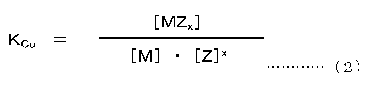
- the stability constant logK Cu is an index indicating the strength of the binding force between the chelating agent and the metal, and can be obtained as a logarithmic value of the equilibrium constant K Cu in the reaction equation represented by the above formula (1).
- K Cu can be obtained by the following formula (2).
- a chelating agent (B) As a chelating agent (B), by compounding a compound having a stability constant logK Cu of 5 or more with copper ions, at least a part of the copper ions generated in the paste forms a complex with the chelating agent (B). I think that. Therefore, it is possible to reduce the amount of copper ions that react with moisture, oxygen, etc. (for example, O 2 , H 2 O, etc.) in the atmosphere, and to suppress the formation of copper oxide in the paste. In addition, since the chelating agent (B) is difficult to dissociate from copper ions, the state of the complex can be maintained for a long time even when left in a high humidity environment. Therefore, the conductive paste can form a conductive film in which an oxide film is hardly formed and an increase in volume resistivity is suppressed.
- the stability constant logK Cu of the chelating agent (B) is less than 5, since the binding force to copper ions is not sufficient, the amount of copper ions that react with moisture, oxygen, etc. in the atmosphere cannot be sufficiently reduced, It becomes difficult to suppress the production of copper oxide. Moreover, when the stability number logK Cu of the chelating agent (B) exceeds 15, the binding force of the chelating agent (B) to the copper ions is too strong, which may inhibit the contact between the copper particles and reduce the conductivity. There is. This is presumably because the chelating agent (B) acts not only on the copper ions present on the surface of the copper particles but also on copper (metal copper).
- the stability constant logK Cu is more preferably 7 to 14.
- the functional group (a) containing a nitrogen atom and the functional group (b) containing an atom having a lone pair other than the nitrogen atom are arranged at the ortho position of the aromatic ring.
- An aromatic compound in which the “nitrogen atom” of the functional group (a) and the “atom having a lone pair” of the functional group (b) are bonded via two or three atoms can be preferably used.
- Examples of the atoms interposed between the “nitrogen atom” of the functional group (a) and the “atom having a lone pair” of the functional group (b) include a carbon atom. That is, as the chelating agent (B), among the aromatic compounds, the nitrogen atom of the functional group (a) and the atom having a lone pair of the functional group (b) have 2 or 3 carbon atoms. Those intervened and bonded are preferably used.
- Suitable examples of the functional group (b) containing an atom other than a nitrogen atom having a lone electron pair include a hydroxyl group and a carboxyl group.
- chelating agent (B) specifically, at least one selected from salicylhydroxamic acid, salicylaldoxime, and o-aminophenol can be used.
- the content of the chelating agent (B) in the conductive paste is preferably 0.01 to 1 part by mass, more preferably 0.05 to 0.5 part by mass with respect to 100 parts by mass of the copper particles (A). preferable.
- the content of the chelating agent (B) is less than 0.01 parts by mass, the effect of suppressing the increase in volume resistivity may not be sufficiently obtained when the conductive film is formed.
- content of a chelating agent (B) exceeds 1 mass part, there exists a possibility that the contact of copper particles may be inhibited and electroconductivity may be reduced.
- thermosetting resin (C) contained in the electrically conductive paste of embodiment of this invention, the well-known thermosetting resin used as a resin binder of a normal electrically conductive paste can be used.
- thermosetting resin (C) a phenol resin, a melamine resin, a urea resin etc. can be used conveniently, for example. Among these, a phenol resin can be particularly preferably used. As the phenol resin, a novolac type phenol resin and a resol type phenol resin can be used, and among these, a resol type phenol resin can be particularly preferably used.
- the above-mentioned thermosetting resin includes diallyl phthalate resin, unsaturated alkyd resin, epoxy resin, isocyanate resin, bismaleidotriazine resin, silicone resin and acrylic resin. You may contain suitably at least 1 type selected from resin.
- the thermosetting resin (C) can be added as long as the cured resin component does not impair the conductivity.
- the content of the thermosetting resin (C) in the conductive paste can be appropriately selected according to the ratio between the volume of the copper particles and the volume of the voids existing between the copper particles.
- the amount is preferably 5 to 50 parts by mass, more preferably 5 to 20 parts by mass with respect to 100 parts by mass of the copper particles (A).
- the content of the thermosetting resin (C) is less than 5 parts by mass, it becomes difficult to obtain sufficient flow characteristics as a conductive paste.
- the content of the thermosetting resin (C) exceeds 50 parts by mass, contact between the copper particles is hindered by the cured resin component, and the volume resistivity of the conductor may be increased.
- ⁇ Organic acid ester or amide (D)> In order to cure the ester or amide (D) of the organic acid contained in the conductive paste of the embodiment of the present invention at a temperature of less than 150 ° C. by promoting the curing of the thermosetting resin (C). Blended.
- the organic acid constituting the ester or amide has a pKa of 1 to 4. If the pKa of the organic acid is less than 1, the storage stability of the conductive paste may be adversely affected. Moreover, when pKa of organic acid exceeds 4, the production
- the pKa of the organic acid is more preferably 1 to 3.
- Organic acids having a pKa of 1 to 4 include oxalic acid (1.27), maleic acid (1.92), malonic acid (2.86), salicylic acid (2.97), and fumaric acid (3.02). , Tartaric acid (3.06), citric acid (3.16), formic acid (3.76) and the like.
- these organic acids having a pKa of 1 to 4 the reasons why esters or amides can be suitably used include the following.
- Organic acid esters and amides are less reactive with metals compared to organic acids and therefore have little effect of corroding metals, and can suppress an increase in volume resistivity of the conductive film after curing.
- the metal in the conductive paste may be corroded to increase the volume resistivity of the conductive film after curing.
- Organic acid esters and amides have little effect on promoting the curing of the thermosetting resin in the paste when the paste is stored, and therefore have little adverse effect on the storage stability (pot life) of the conductive paste.
- Examples of the ester or amide of the organic acid having a pKa of 1 to 4 include formamide, methyl salicylate, methyl formate, ethyl formate, dimethyl oxalate, dimethyl maleate, and dimethyl malonate. Although it is not limited to these, It is preferable that it is at least 1 sort (s) selected from these.
- esters or amides of organic acids having a pKa of 1 to 4 esters or amides of organic acids not containing sulfur (S) can be preferably used. This is because S may react with copper to produce a sulfide, and even an organic acid ester or amide may adversely affect paste storage stability.
- formamide, methyl salicylate, dimethyl oxalate, dimethyl malonate, and dimethyl maleate can be preferably used.
- the content of the organic acid ester or amide (D) in the conductive paste is preferably 0.5 to 15 parts by mass with respect to 100 parts by mass of the thermosetting resin (C). Is more preferable. If the content of the organic acid ester or amide (D) is less than 0.5 parts by mass, the effect of promoting the curing of the resin may not be sufficiently obtained. On the other hand, when content of the said organic acid ester or amide (D) exceeds 15 mass parts, there exists a possibility that the contact of copper particles may be inhibited and electroconductivity may be reduced.
- the conductive paste of the present invention may contain a solvent and various additives (leveling agent, coupling agent, viscosity modifier, antioxidant, adhesive agent, etc.) in addition to the components (A) to (D).
- additives leveling agent, coupling agent, viscosity modifier, antioxidant, adhesive agent, etc.
- Other components such as.) May be included as long as the effects of the present invention are not impaired.
- a solvent capable of dissolving the thermosetting resin in order to obtain a paste body having appropriate fluidity, it is preferable to contain a solvent capable of dissolving the thermosetting resin.
- the solvent contained in the conductive paste examples include cyclohexanone, cyclohexanol, terpineol, ethylene glycol, ethylene glycol monoethyl ether, ethylene glycol monobutyl ether, ethylene glycol monoethyl ether acetate, ethylene glycol monobutyl ether acetate, diethylene glycol, diethylene glycol monoethyl.
- Ether, diethylene glycol monobutyl ether, diethylene glycol monoethyl ether acetate, diethylene glycol monobutyl ether acetate and the like can be suitably used.
- the amount of the solvent contained in the conductive paste is preferably 1 to 10% by mass with respect to the copper particles (A).
- the conductive paste according to the embodiment of the present invention can be obtained by mixing the components (A) to (D) with other components such as a solvent.
- the mixing of the components (A) to (D) can be carried out while heating at a temperature that does not cause curing of the thermosetting resin or volatilization of the solvent.
- the temperature during mixing and stirring is preferably 10 to 40 ° C. More preferably, the temperature is 20 to 30 ° C.
- the temperature at which the conductive paste is formed exceeds 40 ° C.
- the thermosetting resin (C) may be cured in the paste or the particles may be fused. In order to prevent the copper particles from being oxidized during mixing, it is preferable to mix in a container substituted with an inert gas.
- the conductive paste of the present invention described above, it is difficult to oxidize in the air, and it is possible to form a conductive film in which an increase in volume resistivity due to the formation of copper oxide is suppressed as compared with a conventional conductive paste.
- the base material 10 with a conductive film of the present invention has a conductive film 12 formed by curing the above-described conductive paste on a base material 11.
- This base material 10 with a conductive film is formed by applying the conductive paste to the surface of the base material 11 to form a conductive paste film, removing volatile components such as a solvent, and then the thermosetting resin (C ) Is cured to form the conductive film 12.
- a glass substrate As the base material 11, a glass substrate, a plastic base material (for example, a film-like base material made of a polyimide film, a polyester film or the like), a fiber reinforced composite material (a glass fiber reinforced resin substrate or the like), a ceramic substrate, or the like is used. be able to.
- the conductive paste of the present invention is used, the conductive film 12 is formed by curing the thermosetting resin (C) by heating at a temperature of less than 150 ° C. (for example, 120 to 140 ° C.), as will be described later. Therefore, a plastic substrate such as polyester such as polyethylene terephthalate (PET) or polyethylene naphthalate (PEN), polycarbonate, or the like can be particularly preferably used.
- Examples of the method for applying the conductive paste include known methods such as screen printing, roll coating, air knife coating, blade coating, bar coating, gravure coating, die coating, and slide coating. Among these, since a smooth wiring shape in which the occurrence of unevenness on the surface and side surfaces is suppressed can be efficiently formed on the substrate 11, the screen printing method is preferably used.
- the curing of the thermosetting resin (C) can be performed by holding the substrate on which the conductive paste film is formed at a temperature of less than 150 ° C. (for example, 120 to 140 ° C.). By setting the curing temperature to 120 ° C. or higher, the thermosetting resin can be sufficiently cured. On the other hand, by setting the curing temperature to 140 ° C. or lower, curing can be performed without deforming the substrate even when a substrate such as a plastic film is used. Examples of the heating method include warm air heating, thermal radiation, and IR heating. Note that the conductive film may be formed in the air or in a nitrogen atmosphere with a small amount of oxygen.
- the thickness of the conductive film 12 on the substrate 11 is preferably 1 to 200 ⁇ m, and more preferably 5 to 100 ⁇ m, from the viewpoint of ensuring stable conductivity and maintaining the wiring shape. .
- the volume resistivity of the conductive film 12 is preferably 1.0 ⁇ 10 ⁇ 4 ⁇ cm or less. If the volume resistivity of the conductive film 12 exceeds 1.0 ⁇ 10 ⁇ 4 ⁇ cm, there is a possibility that sufficient conductivity cannot be obtained as a conductor for electronic equipment.
- the conductive film 12 is formed using the conductive paste of the present invention described above, an oxide film made of copper oxide is hardly generated, and a conventional base material with a conductive film is formed. In comparison with, a substrate with a conductive film having a low volume resistivity and suppressed increase in volume resistivity even when used for a long time in a high humidity environment can be obtained.
- Examples 1 to 4 are examples of the present invention, and examples 5 to 10 are comparative examples.
- the copper particles were subjected to a reduction treatment to obtain copper particles (A) (surface modified copper particles). That is, first, 3.0 g of formic acid and 9.0 g of a 50 mass% hypophosphorous acid aqueous solution were put into a glass beaker, and the beaker was put in a water bath and kept at 40 ° C.
- copper particles (trade name: “1400 YP”, average primary particle diameter: 7 ⁇ m, manufactured by Mitsui Mining & Smelting Co., Ltd.) are gradually added to this beaker and stirred for 30 minutes to obtain a “copper dispersion”. It was.
- the obtained “copper dispersion liquid” was centrifuged at 3000 rpm for 10 minutes using a centrifuge to collect a precipitate. This precipitate was dispersed in 30 g of distilled water, and the aggregate was precipitated again by centrifugation, thereby separating the precipitate.
- the obtained precipitate was heated at 80 ° C. for 60 minutes under a reduced pressure of ⁇ 35 kPa, and the residual water was volatilized and removed gradually to obtain copper particles (A-1) whose particle surfaces were modified. .
- the surface oxygen concentration ratio O / Cu was calculated by dividing the obtained surface oxygen concentration by the surface copper concentration, the surface oxygen concentration ratio O / Cu of the copper particles (A-1) was 0.16.
- the amount of oxygen in the copper particles (A-1) was 460 ppm as measured using an oximeter (manufactured by LECO, trade name: “ROH-600”).
- Example 1 To a resin solution obtained by mixing 0.74 g of phenol resin (manufactured by Gunei Chemical Co., Ltd., trade name: “Resitop PL 6220”, resin solid content: 58 mass%) and 0.43 g of ethylene glycol monobutyl ether acetate, 0. After adding 005 g and dissolving, 0.0215 g of formamide was added and dissolved. Next, 5.0 g of the copper particles (A-1) was blended in the obtained resin solution and mixed in a mortar to obtain a conductive paste 1.
- phenol resin manufactured by Gunei Chemical Co., Ltd., trade name: “Resitop PL 6220”, resin solid content: 58 mass
- 0.0215 g of formamide was added and dissolved.
- 5.0 g of the copper particles (A-1) was blended in the obtained resin solution and mixed in a mortar to obtain a conductive paste 1.
- This conductive paste 1 was applied to a wiring shape (band shape) having a width of 1 mm and a thickness of 20 ⁇ m on a PET substrate by a screen printing method, and heated at 130 ° C. for 15 minutes to cure the phenol resin.
- the base material 1 with a conductive film having the conductive film 1 was formed.
- Example 2 A conductive paste 2 was obtained in the same manner as in Example 1 except that 0.0215 g of formamide was changed to 0.0215 g of methyl salicylate. Subsequently, it replaced with the electrically conductive paste 1, and apply
- Example 2 A conductive paste 2 was obtained in the same manner as in Example 1 except that 0.0215 g of formamide was changed to 0.0215 g of methyl salicylate. Subsequently, it replaced with the electrically conductive paste 1, and apply
- Example 3 0.005 g of salicylhydroxamic acid was changed to 0.005 g of salicylaldoxime, and 0.0215 g of formamide was changed to 0.0215 g of dimethyl oxalate. Otherwise in the same manner as in Example 1, a conductive paste 3 was obtained. Subsequently, it replaced with the electrically conductive paste 1, and apply
- Example 4 A conductive paste 4 was obtained in the same manner as in Example 3 except that 0.0215 g of dimethyl oxalate was changed to 0.0215 g of dimethyl maleate. Subsequently, it replaced with the electrically conductive paste 3, and applied the electrically conductive paste 4 on the PET board
- Example 5 0.0215 g of formamide was not added to the resin solution. Otherwise in the same manner as in Example 1, a conductive paste 5 was obtained.
- Example 6 A conductive paste 6 was obtained in the same manner as in Example 1 except that 0.0215 g of propylene carbonate was added to the resin solution instead of 0.0215 g of formamide.
- Example 7 A conductive paste 7 was obtained in the same manner as in Example 1 except that 0.0215 g of phenyl acetate was added to the resin solution instead of 0.0215 g of formamide.
- Example 8 A conductive paste 8 was obtained in the same manner as in Example 1 except that 0.0215 g of salicylic acid was added to the resin solution instead of 0.0215 g of formamide.
- Example 9 A conductive paste 9 was obtained in the same manner as in Example 1 except that 0.0215 g of oxalic acid was added to the resin solution instead of 0.0215 g of formamide.
- Example 10 A conductive paste 10 was obtained in the same manner as in Example 1 except that 0.0215 g of maleic acid was added to the resin solution instead of 0.0215 g of formamide.
- conductive pastes 5 to 10 were respectively applied on a PET substrate and heated at 130 ° C. for 15 minutes to form conductive films 5 to 10. Otherwise in the same manner as in Example 1, substrates 5 to 10 with conductive film (Examples 5 to 10) were obtained.
- the resistance values of the obtained conductive films 1 to 10 were measured using a resistance meter (trade name: “Milliohm Hitester” manufactured by Keithley) to determine the initial volume resistivity.
- Durability test Durability tests were conducted on the substrates 1 to 10 with the conductive film in a high-temperature and high-humidity environment. That is, the resistance values of the conductive films 1 to 10 were measured after holding the conductive film-coated substrates 1 to 10 in a bath at 60 ° C. and 90% RH at a high temperature and high humidity for 240 hours. And the volume resistivity after a durability test was calculated
- Table 1 shows the initial volume resistivity thus obtained and the rate of change (increase rate) of the volume resistivity after the durability test.
- curing agent is shown with the addition amount (mass part) with respect to 100 mass parts of solid content of a phenol resin.
- the conductive film substrates 1 to 4 in which the conductive films 1 to 4 are formed from the conductive pastes 1 to 4 containing an ester or amide of an organic acid having a pKa of 1 to 4 (Example 1)
- the volume resistivity was low, and the fluctuation rate (increase rate) of the volume resistivity after the durability test in a high temperature and high humidity environment was also kept low.
- the conductive film bases 8 to 10 (Examples 8 to 10) in which the conductive films 8 to 10 are formed by using the conductive pastes 8 to 10 in which an organic acid itself having a pKa of 1 to 4 is blended instead of an ester or an amide,
- the fluctuation rate of the volume resistivity after the durability test in a high temperature and high humidity environment was as high as 23 to 26%, and the durability was inferior.
- the conductive paste of the present invention can be cured at a temperature lower than the conventional temperature of less than 150 ° C., the formation of copper oxide is suppressed in a high humidity environment, and a low volume resistivity can be maintained for a long time.
- a conductive film can be formed.
- a resin or the like is used as an insulating base material, which is highly reliable as a wiring board or the like, and with a conductive film in which an increase in volume resistivity due to formation of an oxide film is suppressed.
- a substrate can be obtained.
Landscapes
- Chemical & Material Sciences (AREA)
- Engineering & Computer Science (AREA)
- Materials Engineering (AREA)
- Physics & Mathematics (AREA)
- Dispersion Chemistry (AREA)
- Spectroscopy & Molecular Physics (AREA)
- Mechanical Engineering (AREA)
- Metallurgy (AREA)
- Organic Chemistry (AREA)
- Manufacturing & Machinery (AREA)
- Conductive Materials (AREA)
- Parts Printed On Printed Circuit Boards (AREA)
- Manufacturing Of Electric Cables (AREA)
Abstract
Description
(1)銅粒子(A)と、25℃、イオン強度0.1mol/Lにおける銅イオンとの安定度定数logKCuが5~15である化合物からなるキレート剤(B)と、熱硬化性樹脂(C)と、pKaが1~4の有機酸の、エステルまたはアミド(D)を含有することを特徴とする導電ペースト。
(4)前記銅粒子(A)は、平均一次粒子径が0.3~20μmの金属銅粒子表面に、平均一次粒子径が1~20nmの金属銅微粒子が凝集して付着した複合金属銅粒子である(1)乃至(3)のいずれか1つに記載の導電ペースト。
(6)前記窒素原子以外の孤立電子対を有する原子を含む官能基(b)は、水酸基またはカルボキシル基である(5)記載の導電ペースト。
(7)前記窒素原子と前記窒素原子以外の孤立電子対を有する原子とは、2個または3個の原子を介在して結合している(5)または(6)記載の導電ペースト。
(8)前記キレート剤(B)は、サリチルヒドロキサム酸、サリチルアルドキシムおよびo-アミノフェノールからなる群から選択される少なくとも1種である(1)乃至(7)のいずれか1つに記載の導電ペースト。
(10)前記有機酸のエステルまたはアミド(D)は、ホルムアミド、サリチル酸メチル、シュウ酸ジメチル、マロン酸ジメチルおよびマレイン酸ジメチルからなる群から選択される少なくとも1種である(1)乃至(9)のいずれか1つに記載の導電ペースト。
(12)前記熱硬化性樹脂(C)の含有量は、前記銅粒子(A)100質量部に対して5~50質量部である(1)乃至(11)のいずれか1つに記載の導電ペースト。
(13)前記有機酸のエステルまたはアミド(D)の含有量は、前記熱硬化性樹脂(C)100質量部に対して0.5~15質量部である(1)乃至(12)のいずれか1つに記載の導電ペースト。
(15)前記基材は、ポリエチレンテレフタレート(PET)、ポリエチレンナフタレート(PEN)およびポリカーボネートからなる群から選択される少なくとも1種である(14)記載の導電膜付き基材。
(16)前記導電膜の体積抵抗率が1.0×10⁻⁴Ωcm以下である(14)または(15)記載の導電膜付き基材。
本発明の実施形態である導電ペーストは、銅粒子(A)と、25℃、イオン強度0.1mol/Lにおける銅イオンとの安定度定数logKCuが5~15である化合物からなるキレート剤(B)と、熱硬化性樹脂(C)と、pKaが1~4の有機酸のエステルまたはアミド(D)をそれぞれ含有する。
実施形態の導電ペーストは、銅粒子(A)とキレート剤(B)と熱硬化性樹脂(C)、およびpKaが1~4の有機酸の、エステルまたはアミド(D)を含有する。以下、導電ペーストを構成する各成分について説明する。
銅粒子(A)は、導電ペーストの導電成分となるものであり、X線光電子分光法によって求められる表面酸素濃度比O/Cuが0.5以下である。以下、X線光電子分光法によって求められる表面酸素濃度比O/Cuを、単に「表面酸素濃度比O/Cu」と示す。
銅粒子(A)が金属銅粒子を含む場合にその平均粒子径(平均一次粒子径)が0.3μm以上の場合、この銅粒子を含む導電ペーストの流動特性が良好となる。また、銅粒子(A)が銅微粒子のみからなる場合にその凝集粒子の平均粒子径が0.01μm以上の場合には、この銅粒子を含む導電ペーストの流動特性が良好となる。
(A1)金属銅粒子であって、その平均一次粒子径が0.3~20μmである金属銅粒子。
(A2)金属銅粒子であって、その平均一次粒子径が0.3~20μmである金属銅粒子と、上記金属銅粒子表面に付着した水素化銅微粒子であって、その凝集粒子の平均粒子径が20~400nmである水素化銅微粒子と、を有する銅複合粒子。
(A3)水素化銅微粒子であって、その凝集粒子の平均粒子径が10nm~1μmである水素化銅微粒子。
(A4)金属銅粒子であって、その平均一次粒子径が0.3~20μmである金属銅粒子と、上記金属銅粒子表面に付着した水素化銅微粒子を加熱した金属銅微粒子であって、その凝集粒子の平均粒子径が20~400nmである金属銅微粒子と、を有する複合金属銅粒子。
(A5)金属銅微粒子であって、その凝集粒子の平均粒子径が10nm~1μmである金属銅微粒子。
すなわち、金属銅粒子についての平均一次粒子径は、走査型電子顕微鏡(以下、「SEM」と記す。)像の中から無作為に選んだ100個の粒子のFeret径を測定し、これらの粒子径を平均して算出したものである。
また、銅微粒子からなる凝集粒子の平均粒子径は、透過型電子顕微鏡(以下、「TEM」と記す。)像の中から無作為に選んだ100個の粒子のFeret径を測定し、これらの粒子径を平均して算出したものである。
また、例えば銅複合粒子(A2)のように、金属銅粒子である銅粒子と、この銅粒子表面に付着した水素化銅微粒子とを含む複合粒子の場合には、この複合粒子全体をSEMによって観察し、銅微粒子も含む粒子全体のFeret径を測定し、得られた粒子径を平均して算出したものである。
金属銅粒子の平均粒子径が0.3μm未満であると、導電ペーストとしたときに、十分な流動特性を得られない。一方、金属銅粒子の平均粒子径が20μmを超えると、得られる導電ペーストによる、微細配線の作製が困難となるおそれがある。金属銅粒子の平均粒子径は、1~10μmであることがより好ましい。なお、金属銅粒子の平均粒子径は、SEM像の中から無作為に選出した100個の金属銅粒子のFeret径を測定し、この測定値を平均して算出したものである。
水素化銅微粒子の量が、金属銅粒子の量に対して5質量%未満であると、金属銅粒子間に導電パスが十分に形成されず、導電膜の体積抵抗率を低減する効果を十分に得られないおそれがある。一方、水素化銅微粒子の量が、金属銅粒子の量に対して50質量%を超えると、導電ペーストとして十分な流動性を確保するのが困難となる。
なお、金属銅粒子の表面に付着した水素化銅微粒子の量は、例えば、還元剤を加える前の水溶性銅化合物溶液中の銅イオン濃度と、水素化銅微粒子生成終了後の反応液中に残存する銅イオン濃度との差から算出できる。
本発明における「表面改質銅粒子」は、銅粒子表面を、pH値が3以下の分散媒中で還元処理して得られる。「表面改質銅粒子」は、例えば、(1)銅粒子を分散媒に分散して「銅分散液」とする工程、(2)銅分散液のpH値を所定値以下に調整する工程、(3)銅分散液に還元剤を添加する工程、の下記の(1)~(3)の工程を有する、湿式還元法により製造できる。
銅分散液に分散させる銅粒子は、導電ペーストとして一般に用いられる銅粒子を用いることができる。銅分散液に分散させる銅粒子の粒子形状は球状であってもよく、板状であってもよい。
なお、銅粒子の平均粒子径は、SEM像の中から無作為に選出した100個の金属銅粒子のFeret径を測定し、その平均値を算出して得たものである。
上記(1)で得られた銅分散液のpH値を調整する。pH値の調整は、銅分散液にpH調整剤を添加して行うことができる。
銅分散液のpH調整剤としては、酸を使用できる。銅分散液のpH調整剤としては、例えばギ酸、クエン酸、マレイン酸、マロン酸、酢酸、プロピオン酸等のカルボン酸や、硫酸、硝酸、塩酸等の無機酸を好適に使用できる。
pH値を調整した銅分散液に還元剤を添加して還元処理を行う。
銅分散液に添加する還元剤としては、金属水素化物、ヒドリド還元剤、次亜リン酸、次亜リン酸ナトリウムなどの次亜リン酸塩、ジメチルアミンボラン等のアミンボラン、およびギ酸から選ばれる少なくとも1種を使用できる。金属水素化物としては、水素化リチウム、水素化カリウム、および水素化カルシウムが挙げられる。ヒドリド還元剤としては、水素化リチウムアルミニウム、水素化ホウ素リチウム、および水素化ホウ素ナトリウムが挙げられる。これらのうち、次亜リン酸、次亜リン酸ナトリウムを好適に用いることができる。
本発明の実施形態の導電ペーストに含有されるキレート剤(B)は、銅イオンに配位し、下記式(1)で示す反応により銅イオンと錯体を形成し得る化合物からなるものである。

M:銅イオン
Z:キレート剤(B)
MZ:錯塩
x:銅1個と結合するキレート剤(B)の数
上記の分子構造を有する化合物を、キレート剤(B)として配合することで、銅イオンと安定した錯体を形成できる。

キレート剤(B)の含有量が0.01質量部未満であると、導電膜としたとき、体積抵抗率の上昇を抑制する効果を十分に得られないおそれがある。一方、キレート剤(B)の含有量が1質量部を超えると、銅粒子同士の接触を阻害し、導電性を低下させるおそれがある。
本発明の実施形態の導電ペーストに含有される熱硬化性樹脂(C)としては、通常の導電ペーストの樹脂バインダとして用いられる公知の熱硬化性樹脂を用いることができる。
なお、樹脂のガラス転移点(Tg)を調節するために、上述の熱硬化性樹脂中に、ジアリルフェタレート樹脂、不飽和アルキド樹脂、エポキシ樹脂、イソシアネート樹脂、ビスマレイドトリアジン樹脂、シリコーン樹脂およびアクリル樹脂から選択される少なくとも一種を適宜含有してもよい。
導電ペーストにおける熱硬化性樹脂(C)の含有量は、銅粒子の体積と、銅粒子間に存在する空隙の体積との比率に応じて適宜選択できる。銅粒子(A)100質量部に対して5~50質量部であることが好ましく、5~20質量部であることがより好ましい。熱硬化性樹脂(C)の含有量が5質量部未満であると、導電ペーストとして十分な流動特性を得るのが困難となる。一方、熱硬化性樹脂(C)の含有量が50質量部を超えると、硬化後の樹脂成分により銅粒子間の接触が妨げられて、導電体の体積抵抗率を上昇させるおそれがある。
本発明の実施形態の導電ペーストに含有される有機酸の、エステルまたはアミド(D)は、前記熱硬化性樹脂(C)の硬化を促進することで、150℃未満の温度で硬化させるために配合される。エステルまたはアミドを構成する有機酸は、pKaが1~4のものとする。有機酸のpKaが1未満であると、導電ペーストの保存性に悪影響を及ぼすおそれがある。また、有機酸のpKaが4を超えると、前記熱硬化性樹脂(C)の硬化を促進する中間体の生成が遅くなり、結果として樹脂の硬化促進効果が得られないおそれがある。有機酸のpKaは、より好ましくは1~3である。
これらのpKaが1~4である有機酸の中で、エステルまたはアミドが好適に使用できる理由としては、以下のことが挙げられる。
これらのpKaが1~4である有機酸の、エステルまたはアミドの中でも、硫黄(S)を含有しない有機酸の、エステルまたはアミドを好適に使用できる。この理由としては、Sが銅と反応して硫化物を生成するおそれがあるので、有機酸のエステルやアミドであってもペースト保存性に悪影響を与えるおそれがあるからである。具体的には、ホルムアミド、サリチル酸メチル、シュウ酸ジメチル、マロン酸ジメチル、マレイン酸ジメチルを好適に使用できる。
本発明の導電ペーストは、必要に応じて、前記(A)~(D)の各成分に加えて溶剤や各種添加剤(レベリング剤、カップリング剤、粘度調整剤、酸化防止剤、密着剤等。)等のその他の成分を、本発明の効果を損なわない範囲で含んでいてもよい。特に、適度な流動性を有するペースト体を得るために、熱硬化性樹脂を溶解し得る溶剤を含有させることが好ましい。
印刷用ペースト体として適度な粘度範囲とする観点から、導電ペーストに含有させる溶剤の量は、銅粒子(A)に対して1~10質量%が好ましい。
なお、混合時に銅粒子が酸化されるのを防止するため、不活性ガスで置換した容器内で混合することが好ましい。
例えば図1に示すように、本発明の導電膜付き基材10は、基材11上に上述した導電ペーストを硬化させて形成された導電膜12を有する。この導電膜付き基材10は、前記導電ペーストを基材11の表面に塗布して導電ペースト膜を形成し、溶剤等の揮発性成分を除去した後、導電ペースト中の熱硬化性樹脂(C)を硬化させて導電膜12を形成することにより、製造できる。
これらの中でも、表面および側面における凹凸の発生が抑制された滑らかな配線形状を、基材11上に効率的に形成することができるので、スクリーン印刷法が好適に用いられる。
すなわち、まず、ガラス製ビーカーにギ酸3.0gと50質量%次亜リン酸水溶液9.0gとを投入し、このビーカーをウォーターバスに入れて40℃に保持した。
・分析面積:800mm2Φ
・Pass Energy:93.9eV
・Energy Step:0.8eV/step
なお、銅粒子(A-1)中の酸素量を、酸素量計(LECO社製、商品名:「ROH-600」)を用いて測定したところ、460ppmであった。
フェノール樹脂(群栄化学社製、商品名:「レジトップPL6220」、樹脂固形分58質量%)0.74gとエチレングリコールモノブチルエーテルアセテート0.43gとを混合した樹脂溶液に、サリチルヒドロキサム酸0.005gを加えて溶解させた後、ホルムアミド0.0215gを加えて溶解させた。次いで、得られた樹脂溶液に、前記銅粒子(A-1)5.0gを配合し、乳鉢中で混合して導電ペースト1を得た。
ホルムアミド0.0215gをサリチル酸メチル0.0215gに変更したこと以外は、実施例1と同様にして、導電ペースト2を得た。次いで、導電ペースト1に代えて、PET基板上に導電ペースト2を塗布し、導電膜2を形成したこと以外は例1と同様にして、導電膜付き基材2を得た。
サリチルヒドロキサム酸0.005gをサリチルアルドキシム0.005gに変更し、ホルムアミド0.0215gをシュウ酸ジメチル0.0215gに変更した。それ以外は例1と同様にして、導電ペースト3を得た。次いで、導電ペースト1に代えて、PET基板上に導電ペースト3を塗布し、導電膜3を形成したこと以外は例1と同様にして、導電膜付き基材3を得た。
シュウ酸ジメチル0.0215gをマレイン酸ジメチル0.0215gに変更したこと以外は、例3と同様にして、導電ペースト4を得た。次いで、導電ペースト3に代えて、PET基板上に導電ペースト4を塗布し、導電膜4を形成したこと以外は例3と同様にして、導電膜付き基材4を得た。
樹脂溶液にホルムアミド0.0215gを添加しなかった。それ以外は例1と同様にして、導電ペースト5を得た。
ホルムアミド0.0215gに代えて、プロピレンカーボネート0.0215gを樹脂溶液に添加したこと以外は例1と同様にして、導電ペースト6を得た。
ホルムアミド0.0215gに代えて、酢酸フェニル0.0215gを樹脂溶液に添加したこと以外は例1と同様にして、導電ペースト7を得た。
ホルムアミド0.0215gに代えて、サリチル酸0.0215gを樹脂溶液に添加したこと以外は例1と同様にして、導電ペースト8を得た。
ホルムアミド0.0215gに代えて、シュウ酸0.0215gを樹脂溶液に添加したこと以外は例1と同様にして、導電ペースト9を得た。
ホルムアミド0.0215gに代えて、マレイン酸0.0215gを樹脂溶液に添加したこと以外は例1と同様にして、導電ペースト10を得た。
得られた導電膜1~10の抵抗値を、抵抗値計(ケースレー社製、商品名:「ミリオームハイテスタ」)を用いて測定し、初期の体積抵抗率を求めた。
導電膜付き基材1~10について、高温高湿の環境下での耐久性試験を行った。すなわち、導電膜付き基材1~10を60℃、90%RHの高温高湿とした槽内で240時間保持した後、導電膜1~10の抵抗値を測定した。そして、耐久性試験後の体積抵抗率を求めた。
なお、表1において、硬化剤の添加量は、フェノール樹脂の固形分100質量部に対する添加量(質量部)で示したものである。

さらに、エステルまたはアミドではなく、pKaが1~4の有機酸そのものを配合した導電ペースト8~10により導電膜8~10を形成した導電膜付き基材8~10(例8~10)でも、高温高湿環境下での耐久性試験後の体積抵抗率の変動率が23~26%と高くなっており、耐久性に劣るものであった。
本出願は、2011年5月23日出願の日本特許出願2011-114604に基づくものであり、その内容はここに参照として取り込まれる。
Claims (17)
- 銅粒子(A)と、25℃、イオン強度0.1mol/Lにおける銅イオンとの安定度定数logKCuが5~15である化合物からなるキレート剤(B)と、熱硬化性樹脂(C)と、pKaが1~4の有機酸の、エステルまたはアミド(D)を含有することを特徴とする導電ペースト。
- 前記銅粒子(A)は、X線光電子分光法によって求められる表面酸素濃度比O/Cuが0.5以下である請求項1記載の導電ペースト。
- 前記銅粒子(A)は、pH値が3以下の分散媒中で還元処理された表面改質銅粒子である請求項1または2に記載の導電ペースト。
- 前記銅粒子(A)は、平均一次粒子径が0.3~20μmの金属銅粒子表面に、平均一次粒子径が1~20nmの金属銅微粒子が凝集して付着した複合金属銅粒子である請求項1乃至3のいずれか1項記載の導電ペースト。
- 前記キレート剤(B)は、窒素原子を含む官能基(a)と、窒素原子以外の孤立電子対を有する原子を含む官能基(b)とが、芳香環のオルト位に配置された芳香族化合物である請求項1乃至4のいずれか1項記載の導電ペースト。
- 前記窒素原子以外の孤立電子対を有する原子を含む官能基(b)は、水酸基またはカルボキシル基である請求項5記載の導電ペースト。
- 前記窒素原子と前記窒素原子以外の孤立電子対を有する原子とは、2個または3個の原子を介在して結合している請求項5または6記載の導電ペースト。
- 前記キレート剤(B)は、サリチルヒドロキサム酸、サリチルアルドキシムおよびo-アミノフェノールからなる群から選択される少なくとも1種である請求項1乃至7のいずれか1項記載の導電ペースト。
- 前記熱硬化性樹脂(C)は、フェノール樹脂、メラミン樹脂および尿素樹脂からなる群から選択される少なくとも1種である請求項1乃至8のいずれか1項記載の導電ペースト。
- 前記有機酸のエステルまたはアミド(D)は、ホルムアミド、サリチル酸メチル、シュウ酸ジメチル、マロン酸ジメチルおよびマレイン酸ジメチルからなる群から選択される少なくとも1種である請求項1乃至9のいずれか1項記載の導電ペースト。
- 前記キレート剤(B)の含有量は、前記銅粒子(A)100質量部に対して0.01~1質量部である請求項1乃至10のいずれか1項記載の導電ペースト。
- 前記熱硬化性樹脂(C)の含有量は、前記銅粒子(A)100質量部に対して5~50質量部である請求項1乃至11のいずれか1項記載の導電ペースト。
- 前記有機酸のエステルまたはアミド(D)の含有量は、前記熱硬化性樹脂(C)100質量部に対して0.5~15質量部である請求項1乃至12のいずれか1項記載の導電ペースト。
- 基材と、該基材上に請求項1乃至13のいずれか1項記載の導電ペーストを硬化させて形成された導電膜を有する導電膜付き基材。
- 前記基材は、ポリエチレンテレフタレート(PET)、ポリエチレンナフタレート(PEN)およびポリカーボネートからなる群から選択される少なくとも1種である請求項14記載の導電膜付き基材。
- 前記導電膜の体積抵抗率が1.0×10⁻⁴Ωcm以下である請求項14または15記載の導電膜付き基材。
- 請求項1乃至13のいずれか1項記載の導電ペーストを基材上に塗布する工程と、前記導電ペーストを150℃未満の温度で加熱し硬化させて導電膜を形成する工程と、を含む導電膜付き基材の製造方法。
Priority Applications (3)
| Application Number | Priority Date | Filing Date | Title |
|---|---|---|---|
| CN201280025384.1A CN103582918A (zh) | 2011-05-23 | 2012-05-22 | 导电浆料及使用该导电浆料的带导电膜的基材以及带导电膜的基材的制造方法 |
| KR1020137030588A KR20140038413A (ko) | 2011-05-23 | 2012-05-22 | 도전 페이스트 및 이것을 사용한 도전막이 형성된 기재, 그리고 도전막이 형성된 기재의 제조 방법 |
| JP2013516387A JPWO2012161201A1 (ja) | 2011-05-23 | 2012-05-22 | 導電ペーストおよびこれを用いた導電膜付き基材、ならびに導電膜付き基材の製造方法 |
Applications Claiming Priority (2)
| Application Number | Priority Date | Filing Date | Title |
|---|---|---|---|
| JP2011-114604 | 2011-05-23 | ||
| JP2011114604 | 2011-05-23 |
Publications (1)
| Publication Number | Publication Date |
|---|---|
| WO2012161201A1 true WO2012161201A1 (ja) | 2012-11-29 |
Family
ID=47217277
Family Applications (1)
| Application Number | Title | Priority Date | Filing Date |
|---|---|---|---|
| PCT/JP2012/063100 Ceased WO2012161201A1 (ja) | 2011-05-23 | 2012-05-22 | 導電ペーストおよびこれを用いた導電膜付き基材、ならびに導電膜付き基材の製造方法 |
Country Status (5)
| Country | Link |
|---|---|
| JP (1) | JPWO2012161201A1 (ja) |
| KR (1) | KR20140038413A (ja) |
| CN (1) | CN103582918A (ja) |
| TW (1) | TW201301303A (ja) |
| WO (1) | WO2012161201A1 (ja) |
Cited By (4)
| Publication number | Priority date | Publication date | Assignee | Title |
|---|---|---|---|---|
| JP2015049992A (ja) * | 2013-08-30 | 2015-03-16 | 富士フイルム株式会社 | 導電膜形成用組成物およびこれを用いる導電膜の製造方法 |
| JP2015090899A (ja) * | 2013-11-05 | 2015-05-11 | 古河電気工業株式会社 | 接続構造体および該接続構造体を形成するための銅粒子含有ペースト |
| WO2016031860A1 (ja) * | 2014-08-28 | 2016-03-03 | 石原産業株式会社 | 金属質銅粒子及びその製造方法 |
| WO2017029884A1 (ja) * | 2015-08-20 | 2017-02-23 | タツタ電線株式会社 | 導電性組成物 |
Families Citing this family (3)
| Publication number | Priority date | Publication date | Assignee | Title |
|---|---|---|---|---|
| CN111482596B (zh) * | 2015-02-27 | 2022-11-22 | 昭和电工材料株式会社 | 含铜粒子、导体形成组合物、导体的制造方法、导体以及装置 |
| CN108899108A (zh) * | 2018-06-06 | 2018-11-27 | 彩虹集团新能源股份有限公司 | 一种低温触摸屏印刷银浆料及其制备方法 |
| CN113707362A (zh) * | 2021-07-23 | 2021-11-26 | 厦门大学 | 一种高导电铜浆、制备方法、柔性高导电铜膜及其应用 |
Citations (4)
| Publication number | Priority date | Publication date | Assignee | Title |
|---|---|---|---|---|
| JPH01158081A (ja) * | 1987-07-24 | 1989-06-21 | Mitsubishi Petrochem Co Ltd | 銅系導電性塗料組成物 |
| JP2000021235A (ja) * | 1998-07-02 | 2000-01-21 | Mitsui Mining & Smelting Co Ltd | 銅系導電性ペースト |
| JP2002038053A (ja) * | 2000-07-25 | 2002-02-06 | Sumitomo Metal Mining Co Ltd | 透明導電層形成用塗液 |
| JP2006128005A (ja) * | 2004-10-29 | 2006-05-18 | Murata Mfg Co Ltd | 導電性ペーストおよび印刷配線板 |
Family Cites Families (11)
| Publication number | Priority date | Publication date | Assignee | Title |
|---|---|---|---|---|
| JPS62160603A (ja) * | 1986-01-08 | 1987-07-16 | 昭和高分子株式会社 | 導電性ペ−スト |
| JPH05217422A (ja) * | 1992-02-04 | 1993-08-27 | Kao Corp | 導電性ペーストおよび導電性塗膜 |
| JPH05325635A (ja) * | 1992-05-15 | 1993-12-10 | Kao Corp | 導電性ペーストおよび導電性塗膜 |
| JPH06100804A (ja) * | 1992-09-18 | 1994-04-12 | Asahi Chem Ind Co Ltd | 導電性のペースト組成物 |
| JPH09282940A (ja) * | 1996-04-11 | 1997-10-31 | Sumitomo Bakelite Co Ltd | 導電性銅ペースト組成物 |
| JP4460731B2 (ja) * | 2000-07-18 | 2010-05-12 | ハリマ化成株式会社 | 導電性ペースト及びその調製方法 |
| JP4078990B2 (ja) * | 2003-01-23 | 2008-04-23 | 松下電器産業株式会社 | 導電性ペースト、その導電性ペーストを用いた回路形成基板、およびその製造方法 |
| JP2006260951A (ja) * | 2005-03-17 | 2006-09-28 | Osaka Univ | 導電性銅ペースト |
| JP4848674B2 (ja) * | 2005-06-03 | 2011-12-28 | 日本電気株式会社 | 樹脂金属複合導電材料およびその製造方法 |
| WO2009116349A1 (ja) * | 2008-03-21 | 2009-09-24 | 旭硝子株式会社 | 銅ナノ粒子被覆銅フィラー、その製造方法、銅ペーストおよび金属膜を有する物品 |
| WO2012077548A1 (ja) * | 2010-12-10 | 2012-06-14 | 旭硝子株式会社 | 導電ペーストおよびこれを用いた導電膜付き基材、ならびに導電膜付き基材の製造方法 |
-
2012
- 2012-05-22 JP JP2013516387A patent/JPWO2012161201A1/ja not_active Withdrawn
- 2012-05-22 CN CN201280025384.1A patent/CN103582918A/zh active Pending
- 2012-05-22 WO PCT/JP2012/063100 patent/WO2012161201A1/ja not_active Ceased
- 2012-05-22 KR KR1020137030588A patent/KR20140038413A/ko not_active Withdrawn
- 2012-05-23 TW TW101118398A patent/TW201301303A/zh unknown
Patent Citations (4)
| Publication number | Priority date | Publication date | Assignee | Title |
|---|---|---|---|---|
| JPH01158081A (ja) * | 1987-07-24 | 1989-06-21 | Mitsubishi Petrochem Co Ltd | 銅系導電性塗料組成物 |
| JP2000021235A (ja) * | 1998-07-02 | 2000-01-21 | Mitsui Mining & Smelting Co Ltd | 銅系導電性ペースト |
| JP2002038053A (ja) * | 2000-07-25 | 2002-02-06 | Sumitomo Metal Mining Co Ltd | 透明導電層形成用塗液 |
| JP2006128005A (ja) * | 2004-10-29 | 2006-05-18 | Murata Mfg Co Ltd | 導電性ペーストおよび印刷配線板 |
Cited By (6)
| Publication number | Priority date | Publication date | Assignee | Title |
|---|---|---|---|---|
| JP2015049992A (ja) * | 2013-08-30 | 2015-03-16 | 富士フイルム株式会社 | 導電膜形成用組成物およびこれを用いる導電膜の製造方法 |
| JP2015090899A (ja) * | 2013-11-05 | 2015-05-11 | 古河電気工業株式会社 | 接続構造体および該接続構造体を形成するための銅粒子含有ペースト |
| WO2016031860A1 (ja) * | 2014-08-28 | 2016-03-03 | 石原産業株式会社 | 金属質銅粒子及びその製造方法 |
| CN106715009A (zh) * | 2014-08-28 | 2017-05-24 | 石原产业株式会社 | 金属质铜粒子及其制备方法 |
| JPWO2016031860A1 (ja) * | 2014-08-28 | 2017-06-15 | 石原産業株式会社 | 金属質銅粒子及びその製造方法 |
| WO2017029884A1 (ja) * | 2015-08-20 | 2017-02-23 | タツタ電線株式会社 | 導電性組成物 |
Also Published As
| Publication number | Publication date |
|---|---|
| CN103582918A (zh) | 2014-02-12 |
| KR20140038413A (ko) | 2014-03-28 |
| TW201301303A (zh) | 2013-01-01 |
| JPWO2012161201A1 (ja) | 2014-07-31 |
Similar Documents
| Publication | Publication Date | Title |
|---|---|---|
| TWI501260B (zh) | Conductive paste and substrate with conductive film | |
| JP5720693B2 (ja) | 導電性銅粒子の製造方法 | |
| JPWO2012161201A1 (ja) | 導電ペーストおよびこれを用いた導電膜付き基材、ならびに導電膜付き基材の製造方法 | |
| WO2012077548A1 (ja) | 導電ペーストおよびこれを用いた導電膜付き基材、ならびに導電膜付き基材の製造方法 | |
| JP2013140687A (ja) | 導電ペースト、導電膜付き基材およびその製造方法 | |
| JP2013115004A (ja) | 水系銅ペースト材料及び導電層の形成方法 | |
| CN103137243B (zh) | 导电糊剂以及导电糊剂的制备方法 | |
| TWI597345B (zh) | Conductive paste and attached conductive film substrate | |
| JP2017130393A (ja) | 導電性ペーストおよび銀膜の形成方法 | |
| JP2019016592A (ja) | 導電性ペースト | |
| JPWO2012066957A1 (ja) | 導電性組成物、導電膜、及び導電膜の形成方法 | |
| CN104425054B (zh) | 导电性糊剂和带有导电膜的基材 | |
| WO2009098985A1 (ja) | 水素化銅ナノ粒子、その製造方法、金属ペーストおよび物品 | |
| JP2014049191A (ja) | 導電性ペーストおよび導電膜付き基材 | |
| JP2016046136A (ja) | 導電性ペーストおよび導電膜付き基材 | |
| WO2026026052A1 (zh) | 铜浆 | |
| KR20250047267A (ko) | 도전성 페이스트, 전극, 전자 부품 및 전자 기기 | |
| JP2013084411A (ja) | 導電ペーストおよびその製造方法、導電膜付き基材、ならびに導電膜付き基材の製造方法 |
Legal Events
| Date | Code | Title | Description |
|---|---|---|---|
| 121 | Ep: the epo has been informed by wipo that ep was designated in this application |
Ref document number: 12790298 Country of ref document: EP Kind code of ref document: A1 |
|
| ENP | Entry into the national phase |
Ref document number: 2013516387 Country of ref document: JP Kind code of ref document: A |
|
| ENP | Entry into the national phase |
Ref document number: 20137030588 Country of ref document: KR Kind code of ref document: A |
|
| NENP | Non-entry into the national phase |
Ref country code: DE |
|
| 122 | Ep: pct application non-entry in european phase |
Ref document number: 12790298 Country of ref document: EP Kind code of ref document: A1 |