WO2012161026A1 - Procédé de gravure à sec et procédé de fabrication de dispositif - Google Patents
Procédé de gravure à sec et procédé de fabrication de dispositif Download PDFInfo
- Publication number
- WO2012161026A1 WO2012161026A1 PCT/JP2012/062368 JP2012062368W WO2012161026A1 WO 2012161026 A1 WO2012161026 A1 WO 2012161026A1 JP 2012062368 W JP2012062368 W JP 2012062368W WO 2012161026 A1 WO2012161026 A1 WO 2012161026A1
- Authority
- WO
- WIPO (PCT)
- Prior art keywords
- gas
- dry etching
- electrode
- etching
- conductive material
- Prior art date
Links
- 238000000034 method Methods 0.000 title claims description 61
- 238000001312 dry etching Methods 0.000 title claims description 52
- 238000004519 manufacturing process Methods 0.000 title claims description 19
- 238000005530 etching Methods 0.000 claims abstract description 96
- 239000007789 gas Substances 0.000 claims abstract description 88
- MYMOFIZGZYHOMD-UHFFFAOYSA-N Dioxygen Chemical compound O=O MYMOFIZGZYHOMD-UHFFFAOYSA-N 0.000 claims abstract description 42
- 229910001882 dioxygen Inorganic materials 0.000 claims abstract description 42
- 239000004020 conductor Substances 0.000 claims abstract description 30
- 239000003989 dielectric material Substances 0.000 claims abstract description 28
- 238000002156 mixing Methods 0.000 claims abstract description 28
- 239000000463 material Substances 0.000 claims abstract description 16
- 229910052736 halogen Inorganic materials 0.000 claims abstract description 9
- 150000002367 halogens Chemical class 0.000 claims abstract description 9
- 238000000059 patterning Methods 0.000 claims description 21
- 239000000758 substrate Substances 0.000 claims description 16
- 229910000510 noble metal Inorganic materials 0.000 claims description 15
- 239000007769 metal material Substances 0.000 claims description 14
- KZBUYRJDOAKODT-UHFFFAOYSA-N Chlorine Chemical compound ClCl KZBUYRJDOAKODT-UHFFFAOYSA-N 0.000 claims description 11
- 229910052741 iridium Inorganic materials 0.000 claims description 11
- VRIVJOXICYMTAG-IYEMJOQQSA-L iron(ii) gluconate Chemical compound [Fe+2].OC[C@@H](O)[C@@H](O)[C@H](O)[C@@H](O)C([O-])=O.OC[C@@H](O)[C@@H](O)[C@H](O)[C@@H](O)C([O-])=O VRIVJOXICYMTAG-IYEMJOQQSA-L 0.000 claims description 7
- 229910052707 ruthenium Inorganic materials 0.000 claims description 6
- 229910019897 RuOx Inorganic materials 0.000 claims description 5
- 229910002842 PtOx Inorganic materials 0.000 claims description 4
- 229910044991 metal oxide Inorganic materials 0.000 claims description 3
- 150000004706 metal oxides Chemical class 0.000 claims description 3
- 238000010030 laminating Methods 0.000 claims description 2
- 239000013077 target material Substances 0.000 claims 1
- 239000010408 film Substances 0.000 description 44
- 230000000052 comparative effect Effects 0.000 description 29
- 229910052451 lead zirconate titanate Inorganic materials 0.000 description 29
- 229910052760 oxygen Inorganic materials 0.000 description 19
- QVGXLLKOCUKJST-UHFFFAOYSA-N atomic oxygen Chemical compound [O] QVGXLLKOCUKJST-UHFFFAOYSA-N 0.000 description 18
- 239000001301 oxygen Substances 0.000 description 18
- 230000008569 process Effects 0.000 description 12
- ZAMOUSCENKQFHK-UHFFFAOYSA-N Chlorine atom Chemical compound [Cl] ZAMOUSCENKQFHK-UHFFFAOYSA-N 0.000 description 10
- 229910052801 chlorine Inorganic materials 0.000 description 10
- 239000000460 chlorine Substances 0.000 description 10
- BASFCYQUMIYNBI-UHFFFAOYSA-N platinum Substances [Pt] BASFCYQUMIYNBI-UHFFFAOYSA-N 0.000 description 10
- 229910052697 platinum Inorganic materials 0.000 description 7
- XUIMIQQOPSSXEZ-UHFFFAOYSA-N Silicon Chemical compound [Si] XUIMIQQOPSSXEZ-UHFFFAOYSA-N 0.000 description 6
- 238000005229 chemical vapour deposition Methods 0.000 description 6
- 230000000875 corresponding effect Effects 0.000 description 6
- 150000002500 ions Chemical class 0.000 description 6
- 229910052710 silicon Inorganic materials 0.000 description 6
- 239000010703 silicon Substances 0.000 description 6
- VYPSYNLAJGMNEJ-UHFFFAOYSA-N Silicium dioxide Chemical compound O=[Si]=O VYPSYNLAJGMNEJ-UHFFFAOYSA-N 0.000 description 5
- 230000007423 decrease Effects 0.000 description 5
- GKOZUEZYRPOHIO-UHFFFAOYSA-N iridium atom Chemical compound [Ir] GKOZUEZYRPOHIO-UHFFFAOYSA-N 0.000 description 5
- 229910052814 silicon oxide Inorganic materials 0.000 description 5
- 238000004544 sputter deposition Methods 0.000 description 4
- 230000015572 biosynthetic process Effects 0.000 description 3
- 230000007547 defect Effects 0.000 description 3
- 239000011261 inert gas Substances 0.000 description 3
- KJTLSVCANCCWHF-UHFFFAOYSA-N Ruthenium Chemical compound [Ru] KJTLSVCANCCWHF-UHFFFAOYSA-N 0.000 description 2
- BOTDANWDWHJENH-UHFFFAOYSA-N Tetraethyl orthosilicate Chemical compound CCO[Si](OCC)(OCC)OCC BOTDANWDWHJENH-UHFFFAOYSA-N 0.000 description 2
- 238000001636 atomic emission spectroscopy Methods 0.000 description 2
- 238000010586 diagram Methods 0.000 description 2
- 230000000694 effects Effects 0.000 description 2
- 238000002474 experimental method Methods 0.000 description 2
- 230000001965 increasing effect Effects 0.000 description 2
- 229910052751 metal Inorganic materials 0.000 description 2
- 239000002184 metal Substances 0.000 description 2
- 238000007254 oxidation reaction Methods 0.000 description 2
- 238000012545 processing Methods 0.000 description 2
- BSYNRYMUTXBXSQ-UHFFFAOYSA-N Aspirin Chemical compound CC(=O)OC1=CC=CC=C1C(O)=O BSYNRYMUTXBXSQ-UHFFFAOYSA-N 0.000 description 1
- YCKRFDGAMUMZLT-UHFFFAOYSA-N Fluorine atom Chemical compound [F] YCKRFDGAMUMZLT-UHFFFAOYSA-N 0.000 description 1
- 229910052774 Proactinium Inorganic materials 0.000 description 1
- 229910052581 Si3N4 Inorganic materials 0.000 description 1
- 229910004298 SiO 2 Inorganic materials 0.000 description 1
- RTAQQCXQSZGOHL-UHFFFAOYSA-N Titanium Chemical compound [Ti] RTAQQCXQSZGOHL-UHFFFAOYSA-N 0.000 description 1
- 230000001133 acceleration Effects 0.000 description 1
- 238000004380 ashing Methods 0.000 description 1
- 239000003990 capacitor Substances 0.000 description 1
- 239000007795 chemical reaction product Substances 0.000 description 1
- 229910052804 chromium Inorganic materials 0.000 description 1
- 238000001816 cooling Methods 0.000 description 1
- 230000008878 coupling Effects 0.000 description 1
- 238000010168 coupling process Methods 0.000 description 1
- 238000005859 coupling reaction Methods 0.000 description 1
- 238000011161 development Methods 0.000 description 1
- 239000007772 electrode material Substances 0.000 description 1
- 230000002349 favourable effect Effects 0.000 description 1
- 229910052731 fluorine Inorganic materials 0.000 description 1
- 239000011737 fluorine Substances 0.000 description 1
- 239000011521 glass Substances 0.000 description 1
- 230000001939 inductive effect Effects 0.000 description 1
- 229910052746 lanthanum Inorganic materials 0.000 description 1
- FZLIPJUXYLNCLC-UHFFFAOYSA-N lanthanum atom Chemical compound [La] FZLIPJUXYLNCLC-UHFFFAOYSA-N 0.000 description 1
- HFGPZNIAWCZYJU-UHFFFAOYSA-N lead zirconate titanate Chemical compound [O-2].[O-2].[O-2].[O-2].[O-2].[Ti+4].[Zr+4].[Pb+2] HFGPZNIAWCZYJU-UHFFFAOYSA-N 0.000 description 1
- 230000007246 mechanism Effects 0.000 description 1
- 239000000203 mixture Substances 0.000 description 1
- 238000012986 modification Methods 0.000 description 1
- 230000004048 modification Effects 0.000 description 1
- 229910052758 niobium Inorganic materials 0.000 description 1
- 230000003647 oxidation Effects 0.000 description 1
- MUMZUERVLWJKNR-UHFFFAOYSA-N oxoplatinum Chemical compound [Pt]=O MUMZUERVLWJKNR-UHFFFAOYSA-N 0.000 description 1
- 229910003446 platinum oxide Inorganic materials 0.000 description 1
- 238000002360 preparation method Methods 0.000 description 1
- HQVNEWCFYHHQES-UHFFFAOYSA-N silicon nitride Chemical compound N12[Si]34N5[Si]62N3[Si]51N64 HQVNEWCFYHHQES-UHFFFAOYSA-N 0.000 description 1
- 238000003980 solgel method Methods 0.000 description 1
- 238000004611 spectroscopical analysis Methods 0.000 description 1
- 238000004528 spin coating Methods 0.000 description 1
- 239000010409 thin film Substances 0.000 description 1
- 238000007740 vapor deposition Methods 0.000 description 1
Images

Classifications
-
- H—ELECTRICITY
- H10—SEMICONDUCTOR DEVICES; ELECTRIC SOLID-STATE DEVICES NOT OTHERWISE PROVIDED FOR
- H10N—ELECTRIC SOLID-STATE DEVICES NOT OTHERWISE PROVIDED FOR
- H10N30/00—Piezoelectric or electrostrictive devices
- H10N30/01—Manufacture or treatment
- H10N30/09—Forming piezoelectric or electrostrictive materials
- H10N30/093—Forming inorganic materials
-
- B—PERFORMING OPERATIONS; TRANSPORTING
- B41—PRINTING; LINING MACHINES; TYPEWRITERS; STAMPS
- B41J—TYPEWRITERS; SELECTIVE PRINTING MECHANISMS, i.e. MECHANISMS PRINTING OTHERWISE THAN FROM A FORME; CORRECTION OF TYPOGRAPHICAL ERRORS
- B41J2/00—Typewriters or selective printing mechanisms characterised by the printing or marking process for which they are designed
- B41J2/005—Typewriters or selective printing mechanisms characterised by the printing or marking process for which they are designed characterised by bringing liquid or particles selectively into contact with a printing material
- B41J2/01—Ink jet
- B41J2/135—Nozzles
- B41J2/16—Production of nozzles
- B41J2/1607—Production of print heads with piezoelectric elements
- B41J2/161—Production of print heads with piezoelectric elements of film type, deformed by bending and disposed on a diaphragm
-
- B—PERFORMING OPERATIONS; TRANSPORTING
- B41—PRINTING; LINING MACHINES; TYPEWRITERS; STAMPS
- B41J—TYPEWRITERS; SELECTIVE PRINTING MECHANISMS, i.e. MECHANISMS PRINTING OTHERWISE THAN FROM A FORME; CORRECTION OF TYPOGRAPHICAL ERRORS
- B41J2/00—Typewriters or selective printing mechanisms characterised by the printing or marking process for which they are designed
- B41J2/005—Typewriters or selective printing mechanisms characterised by the printing or marking process for which they are designed characterised by bringing liquid or particles selectively into contact with a printing material
- B41J2/01—Ink jet
- B41J2/135—Nozzles
- B41J2/16—Production of nozzles
- B41J2/1621—Manufacturing processes
- B41J2/1626—Manufacturing processes etching
- B41J2/1628—Manufacturing processes etching dry etching
-
- B—PERFORMING OPERATIONS; TRANSPORTING
- B41—PRINTING; LINING MACHINES; TYPEWRITERS; STAMPS
- B41J—TYPEWRITERS; SELECTIVE PRINTING MECHANISMS, i.e. MECHANISMS PRINTING OTHERWISE THAN FROM A FORME; CORRECTION OF TYPOGRAPHICAL ERRORS
- B41J2/00—Typewriters or selective printing mechanisms characterised by the printing or marking process for which they are designed
- B41J2/005—Typewriters or selective printing mechanisms characterised by the printing or marking process for which they are designed characterised by bringing liquid or particles selectively into contact with a printing material
- B41J2/01—Ink jet
- B41J2/135—Nozzles
- B41J2/16—Production of nozzles
- B41J2/1621—Manufacturing processes
- B41J2/164—Manufacturing processes thin film formation
- B41J2/1642—Manufacturing processes thin film formation thin film formation by CVD [chemical vapor deposition]
-
- B—PERFORMING OPERATIONS; TRANSPORTING
- B41—PRINTING; LINING MACHINES; TYPEWRITERS; STAMPS
- B41J—TYPEWRITERS; SELECTIVE PRINTING MECHANISMS, i.e. MECHANISMS PRINTING OTHERWISE THAN FROM A FORME; CORRECTION OF TYPOGRAPHICAL ERRORS
- B41J2/00—Typewriters or selective printing mechanisms characterised by the printing or marking process for which they are designed
- B41J2/005—Typewriters or selective printing mechanisms characterised by the printing or marking process for which they are designed characterised by bringing liquid or particles selectively into contact with a printing material
- B41J2/01—Ink jet
- B41J2/135—Nozzles
- B41J2/16—Production of nozzles
- B41J2/1621—Manufacturing processes
- B41J2/164—Manufacturing processes thin film formation
- B41J2/1645—Manufacturing processes thin film formation thin film formation by spincoating
-
- B—PERFORMING OPERATIONS; TRANSPORTING
- B41—PRINTING; LINING MACHINES; TYPEWRITERS; STAMPS
- B41J—TYPEWRITERS; SELECTIVE PRINTING MECHANISMS, i.e. MECHANISMS PRINTING OTHERWISE THAN FROM A FORME; CORRECTION OF TYPOGRAPHICAL ERRORS
- B41J2/00—Typewriters or selective printing mechanisms characterised by the printing or marking process for which they are designed
- B41J2/005—Typewriters or selective printing mechanisms characterised by the printing or marking process for which they are designed characterised by bringing liquid or particles selectively into contact with a printing material
- B41J2/01—Ink jet
- B41J2/135—Nozzles
- B41J2/16—Production of nozzles
- B41J2/1621—Manufacturing processes
- B41J2/164—Manufacturing processes thin film formation
- B41J2/1646—Manufacturing processes thin film formation thin film formation by sputtering
-
- H—ELECTRICITY
- H01—ELECTRIC ELEMENTS
- H01L—SEMICONDUCTOR DEVICES NOT COVERED BY CLASS H10
- H01L21/00—Processes or apparatus adapted for the manufacture or treatment of semiconductor or solid state devices or of parts thereof
- H01L21/02—Manufacture or treatment of semiconductor devices or of parts thereof
- H01L21/04—Manufacture or treatment of semiconductor devices or of parts thereof the devices having potential barriers, e.g. a PN junction, depletion layer or carrier concentration layer
- H01L21/18—Manufacture or treatment of semiconductor devices or of parts thereof the devices having potential barriers, e.g. a PN junction, depletion layer or carrier concentration layer the devices having semiconductor bodies comprising elements of Group IV of the Periodic Table or AIIIBV compounds with or without impurities, e.g. doping materials
- H01L21/30—Treatment of semiconductor bodies using processes or apparatus not provided for in groups H01L21/20 - H01L21/26
- H01L21/31—Treatment of semiconductor bodies using processes or apparatus not provided for in groups H01L21/20 - H01L21/26 to form insulating layers thereon, e.g. for masking or by using photolithographic techniques; After treatment of these layers; Selection of materials for these layers
- H01L21/3205—Deposition of non-insulating-, e.g. conductive- or resistive-, layers on insulating layers; After-treatment of these layers
- H01L21/321—After treatment
- H01L21/3213—Physical or chemical etching of the layers, e.g. to produce a patterned layer from a pre-deposited extensive layer
- H01L21/32133—Physical or chemical etching of the layers, e.g. to produce a patterned layer from a pre-deposited extensive layer by chemical means only
- H01L21/32135—Physical or chemical etching of the layers, e.g. to produce a patterned layer from a pre-deposited extensive layer by chemical means only by vapour etching only
- H01L21/32136—Physical or chemical etching of the layers, e.g. to produce a patterned layer from a pre-deposited extensive layer by chemical means only by vapour etching only using plasmas
-
- H—ELECTRICITY
- H10—SEMICONDUCTOR DEVICES; ELECTRIC SOLID-STATE DEVICES NOT OTHERWISE PROVIDED FOR
- H10N—ELECTRIC SOLID-STATE DEVICES NOT OTHERWISE PROVIDED FOR
- H10N30/00—Piezoelectric or electrostrictive devices
- H10N30/01—Manufacture or treatment
- H10N30/06—Forming electrodes or interconnections, e.g. leads or terminals
-
- H—ELECTRICITY
- H10—SEMICONDUCTOR DEVICES; ELECTRIC SOLID-STATE DEVICES NOT OTHERWISE PROVIDED FOR
- H10N—ELECTRIC SOLID-STATE DEVICES NOT OTHERWISE PROVIDED FOR
- H10N30/00—Piezoelectric or electrostrictive devices
- H10N30/20—Piezoelectric or electrostrictive devices with electrical input and mechanical output, e.g. functioning as actuators or vibrators
- H10N30/204—Piezoelectric or electrostrictive devices with electrical input and mechanical output, e.g. functioning as actuators or vibrators using bending displacement, e.g. unimorph, bimorph or multimorph cantilever or membrane benders
- H10N30/2047—Membrane type
Definitions
- the present invention relates to a dry etching method and a device manufacturing method, and in particular, a dry etching technique suitable for patterning a metal material in a laminated structure in which a metal material is laminated on a dielectric material, and an actuator, a sensor, etc.
- the present invention relates to a device manufacturing technique for manufacturing various circuit elements.
- Patent Document 1 discloses a technique for patterning an iridium (Ir) -based conductive film, particularly an IrO 2 film, by dry etching using a resist mask (etching-resistant mask layer), and a reaction product having a low vapor pressure is applied to the side wall of the pattern.
- a resist mask etching-resistant mask layer
- a reaction product having a low vapor pressure is applied to the side wall of the pattern.
- Patent Document 2 discloses that a dry etching method of patterning an iridium metal thin film using a resist mask uses an etching gas containing an active gas and a fluorine-based gas.
- Patent Document 3 applies a low-frequency bias power to a film containing a noble metal in a high vacuum, high-density plasma, using a mixed gas of a halogen gas and an inert gas as an etching gas in a dry etching method for a film containing a noble metal.
- a dry etching method without side wall adhesion is provided.
- a piezoelectric body used for a piezoelectric element and a noble metal used for an electrode thereof are said to be difficult to etch materials and are difficult to process by dry etching.
- Such materials are generally etched using a mixed gas of halogen gas or inert gas as described in Patent Documents 2 and 3, but (1) the etching rate is slow.
- problems such as (2) low mask selection ratio of resist or the like, and (3) low selection ratio with the underlying film.
- this laminated upper electrode When patterning is performed, there is a problem that the selection ratio to the piezoelectric body is low and the etching rate is slow.
- Patent Document 1 there is no description regarding the selection ratio with respect to the dielectric as a base film.
- the etching is stopped by emission spectroscopic analysis (OES: Optical Emission Spectroscopy) at the time of Ir etching.
- OES emission spectroscopic analysis
- shape defects occur.
- the dielectric layer is cut, the device characteristics deteriorate.
- Patent Documents 2 and 3 there is no mention of the selection ratio with the base film.
- the above-mentioned problem is common not only for piezoelectric elements but also for a structure in which a metal material is laminated on a dielectric material.
- the present invention has been made in view of such circumstances, and a dry etching method capable of increasing the selection ratio between a metal material and a dielectric serving as a base thereof and improving the etching rate (etching rate), and
- An object is to provide an applied device manufacturing method.
- One embodiment of the present invention is a dry etching method for etching a conductive material stacked on a dielectric material, using a mixed gas containing a halogen gas and an oxygen gas as an etching gas, and mixing the oxygen gas in the mixed gas
- the ratio is 30% or more and 60% or less, and when the mixed gas is supplied into the chamber to generate plasma, the gas pressure in the chamber is set in the range of 1 Pa or more and less than 5 Pa, and the dielectric material has the conductivity.
- the present invention relates to a dry etching method characterized in that etching is performed by applying a bias voltage having a frequency of 800 kHz or more and less than 4 MHz as a bias voltage to a material to be etched.
- the conductive material is patterned by etching using the dry etching method described above, and a device having a structure in which an electrode made of the conductive material and the dielectric material are stacked is manufactured.
- the present invention relates to a device manufacturing method.
- Another aspect of the present invention includes a first electrode forming step of forming a first electrode made of a first conductive material on a substrate, and a dielectric layer forming step of laminating a dielectric material on the first electrode.
- the present invention it is possible to perform an etching process with a high etching rate and a high selection ratio with respect to the dielectric material as the underlayer.
- Example of manufacturing process of piezoelectric element a manufacturing process of the piezoelectric element will be exemplified, and a dry etching method according to an embodiment of the present invention and an upper electrode patterning process using the dry etching method will be described.
- FIG. 1 is an explanatory view showing a manufacturing process of a piezoelectric element.
- Step 1 Substrate Preparation Step First, as shown in FIG. 1A, a silicon (Si) substrate 10 is prepared.
- Step 2 Insulating Film Formation Step Next, an insulating film (for example, an oxide film such as SiO 2 ) 12 is formed on the silicon substrate 10 (FIG. 1B).
- a silicon oxide film is formed by CVD (Chemical Vapor Deposition), sputtering, vapor deposition, thermal oxidation method, or the like.
- Step 3 Lower electrode formation step Next, an adhesion layer (for example, a Ti layer) 14 is formed on the insulating film 12, and a noble metal film corresponding to the lower electrode 16 is formed on the adhesion layer 14 ( FIG. 1 (c)).
- the lower electrode 16 is made of a noble metal material such as Pt (platinum), Ir (iridium), Ru (ruthenium), or an oxide film thereof.
- the lower electrode 16 can be formed by sputtering or CVD.
- a piezoelectric body 18 is formed on the lower electrode 16.
- the piezoelectric body 18 can be formed of a ferroelectric material such as lead zirconate titanate (PZT), and can be formed by a sputtering method, a CVD method, a sol-gel method, or the like. Not only PZT but also lead lanthanum zirconate titanate (PLZT) or “PZTN” in which a part of Ti of PZT is replaced by Nb can be used as the material of the piezoelectric body 18.
- PZT lead lanthanum zirconate titanate
- Nb sol-gel method
- Step 5 Upper electrode forming step Next, a noble metal film corresponding to the upper electrode 20 is formed on the piezoelectric body 18 (FIG. 1E).
- the upper electrode 20 can be formed of Pt, Ir, Ru or an oxide film thereof (PtOx, IrOx, RuOx), and can be formed by a sputtering method or a CVD method.
- PtOx is a generic name for platinum oxide, and “x” represents a positive number indicating the ratio of Pt and O. The same applies to IrOx and RuOx.
- IrOx is a general term for oxides of iridium
- RuOx is a general term for oxides of ruthenium.
- a hard mask 22 that covers the upper electrode 20 is formed (FIG. 1F).
- the hard mask 22 can be formed using a silicon oxide film, a silicon nitride film, an organic SOG (Spin on Glass) film, an inorganic SOG film, or a metal such as Ti, Cr, Al, or Ni.
- a silicon oxide film is formed by TEOS (Tetra Ethyl Ortho Silicate) -CVD method.
- Step 7 Resist Mask Forming Step Next, a resist 24 is formed on the hard mask 22 layer by spin coating or the like, followed by soft baking, exposure and development, and then post baking. In addition, you may perform the hardening process (UV cure) by ultraviolet irradiation instead of post-baking. Thus, the resist 24 for patterning the upper electrode is patterned (FIG. 1G).
- Step 8 Hard Mask Patterning Step
- the hard mask 22 is a silicon oxide film
- the hard mask 22 is patterned by a dry etching method (FIG. 1H).
- Step 9) Resist removal step Thereafter, the resist 24 used in the patterning step of the hard mask 22 is removed using an ashing method or a special stripping solution (FIG. 1 (i)).
- Step 10 Upper electrode patterning step Patterning of the upper electrode 20 is performed by a dry etching method to which one embodiment of the present invention is applied (FIG. 1 (j)).
- the important points in dry etching of the upper electrode 20 are that the etching rate is high, the mask selection ratio and the selection ratio with the dielectric (which is PZT in this example) are high, and the etching shape is It is good. In particular, there is a problem that the base film selection ratio decreases when the etching rate is increased.
- the dry etching method according to this embodiment is a dry etching method that has a high etching rate and can sufficiently ensure a selection ratio with the base film.
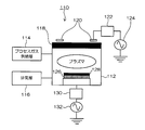
- FIG. 2 is a configuration diagram of a dry etching apparatus using the dry etching method according to the present embodiment.
- the dry etching apparatus 110 for example, an inductive coupling plasma (ICP) apparatus is used.
- ICP inductive coupling plasma
- methods using plasma sources such as Helicon Wave Plasma (HWP), Electron Cyclotron Resonance (ECR) plasma, Surface Wave Plasma (SWP), etc. It is also possible to apply to the dry etching apparatus 110.
- HWP Helicon Wave Plasma
- ECR Electron Cyclotron Resonance
- SWP Surface Wave Plasma
- the dry etching apparatus 110 includes a process gas supply unit 114 that supplies a process gas (etching gas) into the chamber 112 (vacuum vessel), an exhaust unit 116 that exhausts the gas in the chamber 112, and a pressure adjustment in the chamber 112. And a pressure adjusting unit (not shown) for performing.
- the pressure in the chamber 112 is adjusted by exhausting from the exhaust unit 116 while supplying the process gas from the process gas supply unit 114 into the chamber 112.
- a mixed gas of chlorine gas and oxygen gas is used as a process gas (etching gas).
- a dielectric window 118 is hermetically attached to the upper surface of the chamber 112, and a loop coil antenna 120 is installed above the dielectric window 118 (atmosphere side).
- a high frequency power source (RF power source) 124 for generating plasma is connected to the antenna 120 via a matching circuit (matching unit) 122.
- the frequency of the high frequency power supply 124 can use a frequency band of 13.56 MHz or more and 60 MHz or less, for example, 13.56 MHz. Further, the high frequency power supply 124 may be pulse-driven.
- a stage 126 is installed in the chamber 112.
- the stage 126 is provided with a substrate cooling mechanism (not shown) provided with an electrostatic chuck or a clamp, and a substrate 128 to be etched is placed on the stage 126.
- a low frequency power supply 132 for applying a bias is connected to the stage 126 via a matching circuit 130.
- the frequency of the low frequency power supply 132 is 800 kHz or more and 4 MHz or less.
- the frequency of the low frequency power supply 132 is 900 kHz or more and 2 MHz or less.
- a frequency around 1 MHz is preferable as the frequency of the low-frequency power source 132.
- pulse driving means may be provided in the bias power source.
- the bias power source is used by pulse driving, means for synchronizing the pulse period of the power source (high frequency power source 124) of the antenna 120 (for plasma generation) and the bias power source (low frequency power source 132) is used. do it.
- the substrate (the stacked structure shown in FIG. 1 (i)) as the material to be etched is placed on the stage 126 in the chamber 112 of the dry etching apparatus 110 shown in FIG.
- the exhaust gas is exhausted by supplying the mixed gas of chlorine gas and oxygen gas as the etching gas from the process gas supply unit 114, and the inside of the chamber 112 has a predetermined gas pressure (
- the pressure is adjusted so as to be a predetermined value within a range of 1 Pa to 5 Pa, which is 3 Pa in this example.
- required power for example, 500 W power
- high-frequency power source 124 for example, 500 W power
- high-density plasma is generated in the chamber 112.
- a predetermined power for example, a power of 200 W
- the power of the antenna RF power source (high frequency power source 124) is 500 W
- the power of the bias power source (low frequency power source 132) is 200 W
- the power condition is common.
- the addition amount of oxygen gas to the chlorine gas of etching gas (mixing ratio of oxygen gas to the whole) is variable, and the etching rate of Ir and the base film are set.
- the selectivity was determined from the etching rate of PZT.
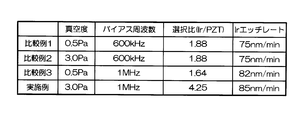
- FIG. 3 summarizes the results of Comparative Examples 1 to 3 and Examples.
- Comparative Example 1 a condition of 600 kHz was used as the frequency of the bias power source (low frequency power source 132).
- the degree of vacuum (gas pressure) in the chamber 112 was 0.5 Pa
- the oxygen flow rate ratio in the etching gas mixed gas of chlorine and oxygen
- Ir on the PZT film was etched.
- the conditions of the bias frequency and the gas pressure in Comparative Example 1 are generally used as etching conditions for noble metal materials such as Ir and Pt.
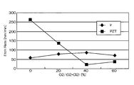
- FIG. 4 and 5 are graphs showing the results when Ir was etched under the conditions of Comparative Example 1.
- FIG. FIG. 4 is a graph showing the relationship between the mixing ratio of oxygen gas in the mixed gas and the etching rates of Ir and PZT.
- the horizontal axis represents the mixing ratio of oxygen gas in the mixed gas of chlorine gas and oxygen gas
- the vertical axis represents the etching rate.
- FIG. 5 is a graph showing the relationship between the mixing ratio of oxygen gas in the mixed gas and the selection ratio (Ir / PZT).
- the horizontal axis represents the mixing ratio of oxygen gas in the mixed gas of chlorine gas and oxygen gas
- the vertical axis represents the selection ratio.
- the etching rate is relatively high as 70 to 105 nm / min, but the selection ratio with respect to PZT as the base film is 0.2 to 1
- the etching rate at that time was 75 nm / min. That is, according to the conditions of Comparative Example 1, the etching rate is as high as 75 nm / min, but the selectivity is as low as 2 or less.
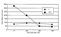
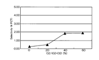
- Comparative Example 2 In Comparative Example 2, the degree of vacuum was set to 3.0 Pa, and Ir was etched under the same conditions as Comparative Example 1 except for other conditions. 6 and 7 are graphs showing the results when Ir was etched under the conditions of Comparative Example 2.
- FIG. FIG. 6 is a graph showing the relationship between the mixing ratio of oxygen gas in the mixed gas and the etching rates of Ir and PZT
- FIG. 7 shows the relationship between the mixing ratio of oxygen gas in the mixed gas and the selection ratio (Ir / PZT). It is a graph.
- the etching rate is 70 to 95 nm / min, which is relatively high, but the selectivity with respect to PZT as the base film is 0.2 to 1.
- the etching rate at that time was 75 nm / min. That is, according to the conditions of Comparative Example 2, the etching rate is as high as 75 nm / min, but the selectivity is as low as 2 or less.
- Comparative Example 3 In Comparative Example 3, the frequency of the bias power supply was set to 1 MHz, and Ir was etched under the same conditions as in Comparative Example 1 under other conditions. 8 and 9 are graphs showing the results when Ir etching was performed under the conditions of Comparative Example 3.
- FIG. FIG. 8 is a graph showing the relationship between the mixing ratio of oxygen gas in the mixed gas and the etching rates of Ir and PZT
- FIG. 9 shows the relationship between the mixing ratio of oxygen gas in the mixed gas and the selection ratio (Ir / PZT). It is a graph.
- the etching rate is relatively high, 60 to 80 nm / min, but the selection ratio with respect to PZT as the base film is 0.2 to 1.
- the etching rate at that time was 82 nm / min. That is, according to the conditions of Comparative Example 3, the etching rate is as high as 75 nm / min, but the selectivity is as low as 2 or less.
- the frequency of the bias power source is 1 MHz
- the degree of vacuum is 3.0 Pa
- a mixed gas of chlorine and oxygen is used, the flow rate ratio is changed
- the high frequency (RF) power source 500 W
- the bias (low frequency) power source Ir was etched under the condition of 200W.
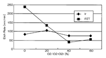
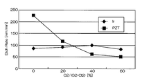
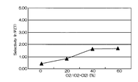
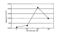
- FIG. 10 and FIG. 11 are graphs showing the results when Ir was etched under the conditions of this example.
- FIG. 10 is a graph showing the relationship between the mixing ratio of oxygen gas in the mixed gas and the etching rates of Ir and PZT
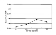
- FIG. 11 shows the relationship between the mixing ratio of oxygen gas and the selection ratio (Ir / PZT) in the mixed gas. It is a graph. As shown in FIGS.
- the etching rate is relatively high, 55 to 85 nm / min.
- the selection ratio with PZT as the base film includes a high value of about 0.2 to 4.25. The highest value was 4.25, and the etching rate at that time was 85 nm / min.
- the mixing ratio of oxygen gas when the mixing ratio of oxygen gas is in the range of 30% to 60%, a high selection ratio of 2 or more can be realized, and the Ir etching rate is also high (see FIG. 10).
- the best condition is when the mixing ratio of oxygen gas is 40%.
- the etching rate is as fast as 85 nm / min, but the selectivity is as high as 4 or more.
- Bias frequency contributes to the amount of ion energy.
- the bias frequency is lower than 800 kHz as in Comparative Example 1, the ion energy is high and the etching of the ferroelectric (PZT) as the base film proceeds, so that a sufficient selection ratio cannot be obtained.
- the bias frequency is 4 MHz or more, the ion energy is low and the noble metal material cannot be etched at high speed.
- the bias frequency is desirably 800 kHz or more and less than 4 MHz, and more desirably approximately 1 MHz.
- a range of “substantially” in the case of approximately 1 MHz an appropriate allowable range can be set within a range in which a corresponding operation effect can be obtained. For example, assuming that ⁇ 15% ( ⁇ 150 kHz) is an allowable range, approximately 1 MHz is a range of 850 kHz to 1.15 MHz, and ⁇ 10% ( ⁇ 100 kHz) is a range of 900 kHz to 1.1 MHz, Further, if ⁇ 5% ( ⁇ 50 kHz) is an allowable range, the range is 950 kHz to 1.05 MHz.
- etching pressure When the etching pressure is less than 1 Pa, the ion energy is high, the etching rate of the ferroelectric film (PZT) as the base film is fast, and a sufficient selection ratio cannot be obtained. On the other hand, when the pressure is 5 Pa or more, a large amount of radicals are generated, the amount of ions is small and the ion energy is low, and the noble metal material cannot be etched sufficiently. From the above, the etching pressure (also referred to as “processing pressure”) is preferably 1 Pa or more and less than 5 Pa, and more preferably about 3 Pa.
- an appropriate allowable range can be set within a range in which a corresponding effect can be obtained. For example, when ⁇ 0.5 Pa is an allowable range, approximately 3 Pa is a range of 3 Pa ⁇ 0.5 Pa, and ⁇ 10% is a range of 3 Pa ⁇ 0.3 Pa when an allowable range is ⁇ 10%.
- Etching gas As the etching gas, a mixed gas of chlorine and oxygen is used. In the case of only chlorine, the etching rate of the ferroelectric film (for example, PZT) which is the base film is fast and the selection ratio cannot be obtained.
- the oxidation reaction of the etchant is performed by adding oxygen gas. That is, Ir, which is a noble metal material, is oxidized to produce oxide IrOx, and the etching rate is improved.
- IrOx is a generic name for oxides of iridium, and “x” represents a positive number indicating the ratio of Ir to O.
- the etching rate of oxides such as ferroelectrics is reduced by the addition of oxygen gas.
- the effect is drastically exhibited at an oxygen addition ratio (oxygen partial pressure) of 30% or more (see FIG. 11).
- oxygen addition ratio oxygen partial pressure
- the amount of oxygen added exceeds 60%, the amount of chlorine as the main etchant decreases, and the Ir etching rate decreases.
- the addition amount (oxygen partial pressure) when adding oxygen to chlorine is 30 to 60%. More preferably, from the viewpoint of realizing a substrate selection ratio of 3 or more, the oxygen addition amount (oxygen partial pressure) is preferably 35% to 50%, and particularly preferably about 40%.
- the range of “substantially” in the case of about 40% an appropriate allowable range can be set within a range in which a corresponding action and effect can be obtained. For example, if ⁇ 5% is an allowable range, approximately 40% is in the range of 35% to 45%.
- the “substantially” range may be determined from the graph of FIG. 11 from the viewpoint of the amount of oxygen added with a selection ratio of 4 or more.
- the desired good etching result can be obtained by the combination of the bias frequency, gas pressure, and etching gas conditions described in [1] to [3] above.
- the bias frequency is about 1 MHz
- oxygen is added to chlorine as an etching gas
- the oxygen partial pressure is 40%
- the degree of vacuum is about 3 Pa
- the Ir etching rate is high and the underlying film is used.
- Etching can be performed while ensuring a sufficient selection ratio of 4 or more with PZT.
- the piezoelectric element manufactured by the process described in FIG. 1 (i) can be used for various applications such as an actuator and a sensor.
- a pressure chamber ink chamber
- a unimorph piezoelectric actuator is configured by a structure in which the lower electrode 16, the piezoelectric body 18, and the upper electrode 20 are laminated on the diaphragm. That is, FIG. 1 can be grasped as an actuator manufacturing process.
- the present invention is not limited to a unimoful type actuator, and can be applied to the manufacture of various types of actuators such as a bimorph actuator.
- the scope of application of the present invention is not limited to the piezoelectric devices exemplified above, and can be widely applied to various devices having a structure in which a dielectric and a conductive material (electrode) are laminated.
- Such devices include various devices such as capacitors, acceleration sensors, temperature sensors, memory devices, pyroelectric devices and the like.
- a dry etching method for etching a conductive material laminated on a dielectric material wherein a mixed gas containing a halogen gas and an oxygen gas is used as an etching gas, and a mixing ratio of oxygen gas in the mixed gas is 30% or more and 60%
- An etching target in which the gas pressure in the chamber when supplying the mixed gas into the chamber to generate plasma is in a range of 1 Pa to less than 5 Pa, and the conductive material is stacked on the dielectric material.
- Etching is performed by applying a bias voltage having a frequency of 800 kHz or more and less than 4 MHz as a bias voltage to the material.
- etching gas It is preferable to use a mixed gas of chlorine gas and oxygen gas as the etching gas.
- the dry etching method of this aspect is a means capable of satisfactorily etching the noble metal material in a structure in which the noble metal material is laminated on the ferroelectric material.
- PZT As the dielectric material, PZT, PLZT, or PZTN can be used.
- the conductive material is any one of Ru, Ir, and Pt, or any of RuOx, IrOx, and PtOx that is an oxide thereof.
- the dry etching method of this aspect is a means for satisfactorily etching a noble metal such as Ru, Ir, or Pt or a metal oxide thereof.
- Such an embodiment is particularly effective in that both a high etching rate and a sufficient selection ratio can be achieved.
- the electrode conductive material
- the occurrence of a shape defect or the like is suppressed.
- the device with the stable characteristic can be manufactured.
- This embodiment is an effective means for manufacturing an actuator.
- the second electrode second conductive material
- the occurrence of a shape defect or the like is suppressed.
Landscapes
- Engineering & Computer Science (AREA)
- Manufacturing & Machinery (AREA)
- Physics & Mathematics (AREA)
- Chemical & Material Sciences (AREA)
- Condensed Matter Physics & Semiconductors (AREA)
- General Chemical & Material Sciences (AREA)
- Chemical Kinetics & Catalysis (AREA)
- General Physics & Mathematics (AREA)
- Plasma & Fusion (AREA)
- Computer Hardware Design (AREA)
- Microelectronics & Electronic Packaging (AREA)
- Power Engineering (AREA)
- Inorganic Chemistry (AREA)
- Drying Of Semiconductors (AREA)
Abstract
L'invention permet d'augmenter la vitesse de gravure d'un matériau conducteur qui est stratifié sur un matériau diélectrique, tout en améliorant la sélectivité du matériau diélectrique qui sert de base. Un mélange gazeux contenant un halogène gazeux et un oxygène gazeux est utilisé comme gaz de gravure. Le ratio de mélange de l'oxygène gaz dans le mélange gazeux est défini à 30-60 % (inclus). La pression de gaz dans une chambre au moment où un plasma est généré en injectant le mélange gazeux dans la chambre est réglée dans la plage comprise entre 1 Pa (inclus) et 5 Pa (exclus). La gravure est effectuée tout en appliquant une tension de polarisation ayant une fréquence supérieure ou égale à 800 kHz mais inférieure à 4 MHz à un matériau à graver dans lequel un matériau conducteur est stratifié sur un matériau diélectrique.
Priority Applications (2)
| Application Number | Priority Date | Filing Date | Title |
|---|---|---|---|
| CN201280024495.0A CN103548122A (zh) | 2011-05-20 | 2012-05-15 | 干法蚀刻方法及器件制造方法 |
| US14/082,756 US20140076842A1 (en) | 2011-05-20 | 2013-11-18 | Dry etching method and device manufacturing method |
Applications Claiming Priority (2)
| Application Number | Priority Date | Filing Date | Title |
|---|---|---|---|
| JP2011113627A JP5766027B2 (ja) | 2011-05-20 | 2011-05-20 | ドライエッチング方法及びデバイス製造方法 |
| JP2011-113627 | 2011-05-20 |
Related Child Applications (1)
| Application Number | Title | Priority Date | Filing Date |
|---|---|---|---|
| US14/082,756 Continuation US20140076842A1 (en) | 2011-05-20 | 2013-11-18 | Dry etching method and device manufacturing method |
Publications (1)
| Publication Number | Publication Date |
|---|---|
| WO2012161026A1 true WO2012161026A1 (fr) | 2012-11-29 |
Family
ID=47217106
Family Applications (1)
| Application Number | Title | Priority Date | Filing Date |
|---|---|---|---|
| PCT/JP2012/062368 WO2012161026A1 (fr) | 2011-05-20 | 2012-05-15 | Procédé de gravure à sec et procédé de fabrication de dispositif |
Country Status (4)
| Country | Link |
|---|---|
| US (1) | US20140076842A1 (fr) |
| JP (1) | JP5766027B2 (fr) |
| CN (1) | CN103548122A (fr) |
| WO (1) | WO2012161026A1 (fr) |
Families Citing this family (3)
| Publication number | Priority date | Publication date | Assignee | Title |
|---|---|---|---|---|
| EP3276689B1 (fr) * | 2015-03-24 | 2021-05-05 | Sumitomo Chemical Company, Limited | Procédé de fabrication d'un élément de film mince ferroélectrique à base de niobate |
| JP2016184692A (ja) * | 2015-03-26 | 2016-10-20 | 住友化学株式会社 | 強誘電体薄膜素子の製造方法 |
| JP6610883B2 (ja) * | 2015-12-17 | 2019-11-27 | セイコーエプソン株式会社 | 超音波センサー用の圧電デバイス |
Citations (5)
| Publication number | Priority date | Publication date | Assignee | Title |
|---|---|---|---|---|
| JP2002537653A (ja) * | 1999-02-17 | 2002-11-05 | アプライド マテリアルズ インコーポレイテッド | 異方性プロファイルのためのイリジウムエッチング方法 |
| JP2006060203A (ja) * | 2004-08-20 | 2006-03-02 | Sharp Corp | FeRAM用途のためのPt/PGOエッチングプロセス |
| JP2007266466A (ja) * | 2006-03-29 | 2007-10-11 | Tokyo Electron Ltd | プラズマエッチング方法、プラズマエッチング装置、コンピュータ記憶媒体及び処理レシピが記憶された記憶媒体 |
| JP2009231405A (ja) * | 2008-03-21 | 2009-10-08 | Fujifilm Corp | 圧電素子及びその製造方法 |
| JP2010219153A (ja) * | 2009-03-13 | 2010-09-30 | Fujifilm Corp | 圧電素子及びその製造方法並びにインクジェットヘッド |
Family Cites Families (4)
| Publication number | Priority date | Publication date | Assignee | Title |
|---|---|---|---|---|
| KR100413649B1 (ko) * | 1996-01-26 | 2004-04-28 | 마츠시타 덴끼 산교 가부시키가이샤 | 반도체장치의제조방법 |
| JP2002009046A (ja) * | 2000-06-19 | 2002-01-11 | Matsushita Electric Ind Co Ltd | ドライエッチング方法及びそれを用いた容量形成方法 |
| US6942813B2 (en) * | 2003-03-05 | 2005-09-13 | Applied Materials, Inc. | Method of etching magnetic and ferroelectric materials using a pulsed bias source |
| US7985603B2 (en) * | 2008-02-04 | 2011-07-26 | Texas Instruments Incorporated | Ferroelectric capacitor manufacturing process |
-
2011
- 2011-05-20 JP JP2011113627A patent/JP5766027B2/ja active Active
-
2012
- 2012-05-15 WO PCT/JP2012/062368 patent/WO2012161026A1/fr active Application Filing
- 2012-05-15 CN CN201280024495.0A patent/CN103548122A/zh active Pending
-
2013
- 2013-11-18 US US14/082,756 patent/US20140076842A1/en not_active Abandoned
Patent Citations (5)
| Publication number | Priority date | Publication date | Assignee | Title |
|---|---|---|---|---|
| JP2002537653A (ja) * | 1999-02-17 | 2002-11-05 | アプライド マテリアルズ インコーポレイテッド | 異方性プロファイルのためのイリジウムエッチング方法 |
| JP2006060203A (ja) * | 2004-08-20 | 2006-03-02 | Sharp Corp | FeRAM用途のためのPt/PGOエッチングプロセス |
| JP2007266466A (ja) * | 2006-03-29 | 2007-10-11 | Tokyo Electron Ltd | プラズマエッチング方法、プラズマエッチング装置、コンピュータ記憶媒体及び処理レシピが記憶された記憶媒体 |
| JP2009231405A (ja) * | 2008-03-21 | 2009-10-08 | Fujifilm Corp | 圧電素子及びその製造方法 |
| JP2010219153A (ja) * | 2009-03-13 | 2010-09-30 | Fujifilm Corp | 圧電素子及びその製造方法並びにインクジェットヘッド |
Also Published As
| Publication number | Publication date |
|---|---|
| JP2012243992A (ja) | 2012-12-10 |
| US20140076842A1 (en) | 2014-03-20 |
| JP5766027B2 (ja) | 2015-08-19 |
| CN103548122A (zh) | 2014-01-29 |
Similar Documents
| Publication | Publication Date | Title |
|---|---|---|
| US8053955B2 (en) | Piezoelectric device and method of production thereof | |
| TWI667697B (zh) | Substrate processing system and substrate processing method | |
| US20070188976A1 (en) | Capacitor and its manufacturing method | |
| US20030077843A1 (en) | Method of etching conductive layers for capacitor and semiconductor device fabrication | |
| JP5595134B2 (ja) | ドライエッチング装置及びドライエッチング方法 | |
| JP5766027B2 (ja) | ドライエッチング方法及びデバイス製造方法 | |
| JP4999185B2 (ja) | ドライエッチング方法及びドライエッチング装置 | |
| JP2009226660A (ja) | ドライエッチングによるパターニング方法及びそれに用いるモールド並びにインクジェットヘッドの製造方法 | |
| WO2003012851A2 (fr) | Procede de gravure de couches ferroelectriques | |
| WO2012086169A1 (fr) | Procédé de fabrication d'un dispositif diélectrique et procédé de cendrage | |
| JP2006060203A (ja) | FeRAM用途のためのPt/PGOエッチングプロセス | |
| JP5733943B2 (ja) | 誘電体デバイスの製造方法 | |
| JP2012243992A5 (fr) | ||
| JP2011100865A (ja) | プラズマ処理方法 | |
| JP5800710B2 (ja) | 圧電素子の製造方法 | |
| WO2012057127A1 (fr) | Procédé de fabrication d'un dispositif diélectrique | |
| JP2012114156A (ja) | 圧電素子の製造方法 | |
| JP2014060210A (ja) | ドライエッチング方法および圧電デバイスの製造方法 | |
| JP4350120B2 (ja) | ダイヤモンドのエッチング方法 | |
| JP3896123B2 (ja) | 半導体装置の製造方法 | |
| JP5731313B2 (ja) | プラズマエッチング装置、及び誘電体デバイスの製造方法 | |
| JPH113881A (ja) | アッシング方法及び装置 | |
| JP2012156348A (ja) | 誘電体デバイスの製造方法及びエッチング方法 | |
| JP2006294845A (ja) | ドライエッチング方法およびその装置 |
Legal Events
| Date | Code | Title | Description |
|---|---|---|---|
| 121 | Ep: the epo has been informed by wipo that ep was designated in this application |
Ref document number: 12789394 Country of ref document: EP Kind code of ref document: A1 |
|
| NENP | Non-entry into the national phase |
Ref country code: DE |
|
| 122 | Ep: pct application non-entry in european phase |
Ref document number: 12789394 Country of ref document: EP Kind code of ref document: A1 |