WO2012161026A1 - Dry etching method and method for manufacturing device - Google Patents
Dry etching method and method for manufacturing device Download PDFInfo
- Publication number
- WO2012161026A1 WO2012161026A1 PCT/JP2012/062368 JP2012062368W WO2012161026A1 WO 2012161026 A1 WO2012161026 A1 WO 2012161026A1 JP 2012062368 W JP2012062368 W JP 2012062368W WO 2012161026 A1 WO2012161026 A1 WO 2012161026A1
- Authority
- WO
- WIPO (PCT)
- Prior art keywords
- gas
- dry etching
- electrode
- etching
- conductive material
- Prior art date
Links
- 238000000034 method Methods 0.000 title claims description 61
- 238000001312 dry etching Methods 0.000 title claims description 52
- 238000004519 manufacturing process Methods 0.000 title claims description 19
- 238000005530 etching Methods 0.000 claims abstract description 96
- 239000007789 gas Substances 0.000 claims abstract description 88
- MYMOFIZGZYHOMD-UHFFFAOYSA-N Dioxygen Chemical compound O=O MYMOFIZGZYHOMD-UHFFFAOYSA-N 0.000 claims abstract description 42
- 229910001882 dioxygen Inorganic materials 0.000 claims abstract description 42
- 239000004020 conductor Substances 0.000 claims abstract description 30
- 239000003989 dielectric material Substances 0.000 claims abstract description 28
- 238000002156 mixing Methods 0.000 claims abstract description 28
- 239000000463 material Substances 0.000 claims abstract description 16
- 229910052736 halogen Inorganic materials 0.000 claims abstract description 9
- 150000002367 halogens Chemical class 0.000 claims abstract description 9
- 238000000059 patterning Methods 0.000 claims description 21
- 239000000758 substrate Substances 0.000 claims description 16
- 229910000510 noble metal Inorganic materials 0.000 claims description 15
- 239000007769 metal material Substances 0.000 claims description 14
- KZBUYRJDOAKODT-UHFFFAOYSA-N Chlorine Chemical compound ClCl KZBUYRJDOAKODT-UHFFFAOYSA-N 0.000 claims description 11
- 229910052741 iridium Inorganic materials 0.000 claims description 11
- VRIVJOXICYMTAG-IYEMJOQQSA-L iron(ii) gluconate Chemical compound [Fe+2].OC[C@@H](O)[C@@H](O)[C@H](O)[C@@H](O)C([O-])=O.OC[C@@H](O)[C@@H](O)[C@H](O)[C@@H](O)C([O-])=O VRIVJOXICYMTAG-IYEMJOQQSA-L 0.000 claims description 7
- 229910052707 ruthenium Inorganic materials 0.000 claims description 6
- 229910019897 RuOx Inorganic materials 0.000 claims description 5
- 229910002842 PtOx Inorganic materials 0.000 claims description 4
- 229910044991 metal oxide Inorganic materials 0.000 claims description 3
- 150000004706 metal oxides Chemical class 0.000 claims description 3
- 238000010030 laminating Methods 0.000 claims description 2
- 239000013077 target material Substances 0.000 claims 1
- 239000010408 film Substances 0.000 description 44
- 230000000052 comparative effect Effects 0.000 description 29
- 229910052451 lead zirconate titanate Inorganic materials 0.000 description 29
- 229910052760 oxygen Inorganic materials 0.000 description 19
- QVGXLLKOCUKJST-UHFFFAOYSA-N atomic oxygen Chemical compound [O] QVGXLLKOCUKJST-UHFFFAOYSA-N 0.000 description 18
- 239000001301 oxygen Substances 0.000 description 18
- 230000008569 process Effects 0.000 description 12
- ZAMOUSCENKQFHK-UHFFFAOYSA-N Chlorine atom Chemical compound [Cl] ZAMOUSCENKQFHK-UHFFFAOYSA-N 0.000 description 10
- 229910052801 chlorine Inorganic materials 0.000 description 10
- 239000000460 chlorine Substances 0.000 description 10
- BASFCYQUMIYNBI-UHFFFAOYSA-N platinum Substances [Pt] BASFCYQUMIYNBI-UHFFFAOYSA-N 0.000 description 10
- 229910052697 platinum Inorganic materials 0.000 description 7
- XUIMIQQOPSSXEZ-UHFFFAOYSA-N Silicon Chemical compound [Si] XUIMIQQOPSSXEZ-UHFFFAOYSA-N 0.000 description 6
- 238000005229 chemical vapour deposition Methods 0.000 description 6
- 230000000875 corresponding effect Effects 0.000 description 6
- 150000002500 ions Chemical class 0.000 description 6
- 229910052710 silicon Inorganic materials 0.000 description 6
- 239000010703 silicon Substances 0.000 description 6
- VYPSYNLAJGMNEJ-UHFFFAOYSA-N Silicium dioxide Chemical compound O=[Si]=O VYPSYNLAJGMNEJ-UHFFFAOYSA-N 0.000 description 5
- 230000007423 decrease Effects 0.000 description 5
- GKOZUEZYRPOHIO-UHFFFAOYSA-N iridium atom Chemical compound [Ir] GKOZUEZYRPOHIO-UHFFFAOYSA-N 0.000 description 5
- 229910052814 silicon oxide Inorganic materials 0.000 description 5
- 238000004544 sputter deposition Methods 0.000 description 4
- 230000015572 biosynthetic process Effects 0.000 description 3
- 230000007547 defect Effects 0.000 description 3
- 239000011261 inert gas Substances 0.000 description 3
- KJTLSVCANCCWHF-UHFFFAOYSA-N Ruthenium Chemical compound [Ru] KJTLSVCANCCWHF-UHFFFAOYSA-N 0.000 description 2
- BOTDANWDWHJENH-UHFFFAOYSA-N Tetraethyl orthosilicate Chemical compound CCO[Si](OCC)(OCC)OCC BOTDANWDWHJENH-UHFFFAOYSA-N 0.000 description 2
- 238000001636 atomic emission spectroscopy Methods 0.000 description 2
- 238000010586 diagram Methods 0.000 description 2
- 230000000694 effects Effects 0.000 description 2
- 238000002474 experimental method Methods 0.000 description 2
- 230000001965 increasing effect Effects 0.000 description 2
- 229910052751 metal Inorganic materials 0.000 description 2
- 239000002184 metal Substances 0.000 description 2
- 238000007254 oxidation reaction Methods 0.000 description 2
- 238000012545 processing Methods 0.000 description 2
- BSYNRYMUTXBXSQ-UHFFFAOYSA-N Aspirin Chemical compound CC(=O)OC1=CC=CC=C1C(O)=O BSYNRYMUTXBXSQ-UHFFFAOYSA-N 0.000 description 1
- YCKRFDGAMUMZLT-UHFFFAOYSA-N Fluorine atom Chemical compound [F] YCKRFDGAMUMZLT-UHFFFAOYSA-N 0.000 description 1
- 229910052774 Proactinium Inorganic materials 0.000 description 1
- 229910052581 Si3N4 Inorganic materials 0.000 description 1
- 229910004298 SiO 2 Inorganic materials 0.000 description 1
- RTAQQCXQSZGOHL-UHFFFAOYSA-N Titanium Chemical compound [Ti] RTAQQCXQSZGOHL-UHFFFAOYSA-N 0.000 description 1
- 230000001133 acceleration Effects 0.000 description 1
- 238000004380 ashing Methods 0.000 description 1
- 239000003990 capacitor Substances 0.000 description 1
- 239000007795 chemical reaction product Substances 0.000 description 1
- 229910052804 chromium Inorganic materials 0.000 description 1
- 238000001816 cooling Methods 0.000 description 1
- 230000008878 coupling Effects 0.000 description 1
- 238000010168 coupling process Methods 0.000 description 1
- 238000005859 coupling reaction Methods 0.000 description 1
- 238000011161 development Methods 0.000 description 1
- 239000007772 electrode material Substances 0.000 description 1
- 230000002349 favourable effect Effects 0.000 description 1
- 229910052731 fluorine Inorganic materials 0.000 description 1
- 239000011737 fluorine Substances 0.000 description 1
- 239000011521 glass Substances 0.000 description 1
- 230000001939 inductive effect Effects 0.000 description 1
- 229910052746 lanthanum Inorganic materials 0.000 description 1
- FZLIPJUXYLNCLC-UHFFFAOYSA-N lanthanum atom Chemical compound [La] FZLIPJUXYLNCLC-UHFFFAOYSA-N 0.000 description 1
- HFGPZNIAWCZYJU-UHFFFAOYSA-N lead zirconate titanate Chemical compound [O-2].[O-2].[O-2].[O-2].[O-2].[Ti+4].[Zr+4].[Pb+2] HFGPZNIAWCZYJU-UHFFFAOYSA-N 0.000 description 1
- 230000007246 mechanism Effects 0.000 description 1
- 239000000203 mixture Substances 0.000 description 1
- 238000012986 modification Methods 0.000 description 1
- 230000004048 modification Effects 0.000 description 1
- 229910052758 niobium Inorganic materials 0.000 description 1
- 230000003647 oxidation Effects 0.000 description 1
- MUMZUERVLWJKNR-UHFFFAOYSA-N oxoplatinum Chemical compound [Pt]=O MUMZUERVLWJKNR-UHFFFAOYSA-N 0.000 description 1
- 229910003446 platinum oxide Inorganic materials 0.000 description 1
- 238000002360 preparation method Methods 0.000 description 1
- HQVNEWCFYHHQES-UHFFFAOYSA-N silicon nitride Chemical compound N12[Si]34N5[Si]62N3[Si]51N64 HQVNEWCFYHHQES-UHFFFAOYSA-N 0.000 description 1
- 238000003980 solgel method Methods 0.000 description 1
- 238000004611 spectroscopical analysis Methods 0.000 description 1
- 238000004528 spin coating Methods 0.000 description 1
- 239000010409 thin film Substances 0.000 description 1
- 238000007740 vapor deposition Methods 0.000 description 1
Images

Classifications
-
- H—ELECTRICITY
- H10—SEMICONDUCTOR DEVICES; ELECTRIC SOLID-STATE DEVICES NOT OTHERWISE PROVIDED FOR
- H10N—ELECTRIC SOLID-STATE DEVICES NOT OTHERWISE PROVIDED FOR
- H10N30/00—Piezoelectric or electrostrictive devices
- H10N30/01—Manufacture or treatment
- H10N30/09—Forming piezoelectric or electrostrictive materials
- H10N30/093—Forming inorganic materials
-
- B—PERFORMING OPERATIONS; TRANSPORTING
- B41—PRINTING; LINING MACHINES; TYPEWRITERS; STAMPS
- B41J—TYPEWRITERS; SELECTIVE PRINTING MECHANISMS, i.e. MECHANISMS PRINTING OTHERWISE THAN FROM A FORME; CORRECTION OF TYPOGRAPHICAL ERRORS
- B41J2/00—Typewriters or selective printing mechanisms characterised by the printing or marking process for which they are designed
- B41J2/005—Typewriters or selective printing mechanisms characterised by the printing or marking process for which they are designed characterised by bringing liquid or particles selectively into contact with a printing material
- B41J2/01—Ink jet
- B41J2/135—Nozzles
- B41J2/16—Production of nozzles
- B41J2/1607—Production of print heads with piezoelectric elements
- B41J2/161—Production of print heads with piezoelectric elements of film type, deformed by bending and disposed on a diaphragm
-
- B—PERFORMING OPERATIONS; TRANSPORTING
- B41—PRINTING; LINING MACHINES; TYPEWRITERS; STAMPS
- B41J—TYPEWRITERS; SELECTIVE PRINTING MECHANISMS, i.e. MECHANISMS PRINTING OTHERWISE THAN FROM A FORME; CORRECTION OF TYPOGRAPHICAL ERRORS
- B41J2/00—Typewriters or selective printing mechanisms characterised by the printing or marking process for which they are designed
- B41J2/005—Typewriters or selective printing mechanisms characterised by the printing or marking process for which they are designed characterised by bringing liquid or particles selectively into contact with a printing material
- B41J2/01—Ink jet
- B41J2/135—Nozzles
- B41J2/16—Production of nozzles
- B41J2/1621—Manufacturing processes
- B41J2/1626—Manufacturing processes etching
- B41J2/1628—Manufacturing processes etching dry etching
-
- B—PERFORMING OPERATIONS; TRANSPORTING
- B41—PRINTING; LINING MACHINES; TYPEWRITERS; STAMPS
- B41J—TYPEWRITERS; SELECTIVE PRINTING MECHANISMS, i.e. MECHANISMS PRINTING OTHERWISE THAN FROM A FORME; CORRECTION OF TYPOGRAPHICAL ERRORS
- B41J2/00—Typewriters or selective printing mechanisms characterised by the printing or marking process for which they are designed
- B41J2/005—Typewriters or selective printing mechanisms characterised by the printing or marking process for which they are designed characterised by bringing liquid or particles selectively into contact with a printing material
- B41J2/01—Ink jet
- B41J2/135—Nozzles
- B41J2/16—Production of nozzles
- B41J2/1621—Manufacturing processes
- B41J2/164—Manufacturing processes thin film formation
- B41J2/1642—Manufacturing processes thin film formation thin film formation by CVD [chemical vapor deposition]
-
- B—PERFORMING OPERATIONS; TRANSPORTING
- B41—PRINTING; LINING MACHINES; TYPEWRITERS; STAMPS
- B41J—TYPEWRITERS; SELECTIVE PRINTING MECHANISMS, i.e. MECHANISMS PRINTING OTHERWISE THAN FROM A FORME; CORRECTION OF TYPOGRAPHICAL ERRORS
- B41J2/00—Typewriters or selective printing mechanisms characterised by the printing or marking process for which they are designed
- B41J2/005—Typewriters or selective printing mechanisms characterised by the printing or marking process for which they are designed characterised by bringing liquid or particles selectively into contact with a printing material
- B41J2/01—Ink jet
- B41J2/135—Nozzles
- B41J2/16—Production of nozzles
- B41J2/1621—Manufacturing processes
- B41J2/164—Manufacturing processes thin film formation
- B41J2/1645—Manufacturing processes thin film formation thin film formation by spincoating
-
- B—PERFORMING OPERATIONS; TRANSPORTING
- B41—PRINTING; LINING MACHINES; TYPEWRITERS; STAMPS
- B41J—TYPEWRITERS; SELECTIVE PRINTING MECHANISMS, i.e. MECHANISMS PRINTING OTHERWISE THAN FROM A FORME; CORRECTION OF TYPOGRAPHICAL ERRORS
- B41J2/00—Typewriters or selective printing mechanisms characterised by the printing or marking process for which they are designed
- B41J2/005—Typewriters or selective printing mechanisms characterised by the printing or marking process for which they are designed characterised by bringing liquid or particles selectively into contact with a printing material
- B41J2/01—Ink jet
- B41J2/135—Nozzles
- B41J2/16—Production of nozzles
- B41J2/1621—Manufacturing processes
- B41J2/164—Manufacturing processes thin film formation
- B41J2/1646—Manufacturing processes thin film formation thin film formation by sputtering
-
- H—ELECTRICITY
- H01—ELECTRIC ELEMENTS
- H01L—SEMICONDUCTOR DEVICES NOT COVERED BY CLASS H10
- H01L21/00—Processes or apparatus adapted for the manufacture or treatment of semiconductor or solid state devices or of parts thereof
- H01L21/02—Manufacture or treatment of semiconductor devices or of parts thereof
- H01L21/04—Manufacture or treatment of semiconductor devices or of parts thereof the devices having at least one potential-jump barrier or surface barrier, e.g. PN junction, depletion layer or carrier concentration layer
- H01L21/18—Manufacture or treatment of semiconductor devices or of parts thereof the devices having at least one potential-jump barrier or surface barrier, e.g. PN junction, depletion layer or carrier concentration layer the devices having semiconductor bodies comprising elements of Group IV of the Periodic System or AIIIBV compounds with or without impurities, e.g. doping materials
- H01L21/30—Treatment of semiconductor bodies using processes or apparatus not provided for in groups H01L21/20 - H01L21/26
- H01L21/31—Treatment of semiconductor bodies using processes or apparatus not provided for in groups H01L21/20 - H01L21/26 to form insulating layers thereon, e.g. for masking or by using photolithographic techniques; After treatment of these layers; Selection of materials for these layers
- H01L21/3205—Deposition of non-insulating-, e.g. conductive- or resistive-, layers on insulating layers; After-treatment of these layers
- H01L21/321—After treatment
- H01L21/3213—Physical or chemical etching of the layers, e.g. to produce a patterned layer from a pre-deposited extensive layer
- H01L21/32133—Physical or chemical etching of the layers, e.g. to produce a patterned layer from a pre-deposited extensive layer by chemical means only
- H01L21/32135—Physical or chemical etching of the layers, e.g. to produce a patterned layer from a pre-deposited extensive layer by chemical means only by vapour etching only
- H01L21/32136—Physical or chemical etching of the layers, e.g. to produce a patterned layer from a pre-deposited extensive layer by chemical means only by vapour etching only using plasmas
-
- H—ELECTRICITY
- H10—SEMICONDUCTOR DEVICES; ELECTRIC SOLID-STATE DEVICES NOT OTHERWISE PROVIDED FOR
- H10N—ELECTRIC SOLID-STATE DEVICES NOT OTHERWISE PROVIDED FOR
- H10N30/00—Piezoelectric or electrostrictive devices
- H10N30/01—Manufacture or treatment
- H10N30/06—Forming electrodes or interconnections, e.g. leads or terminals
-
- H—ELECTRICITY
- H10—SEMICONDUCTOR DEVICES; ELECTRIC SOLID-STATE DEVICES NOT OTHERWISE PROVIDED FOR
- H10N—ELECTRIC SOLID-STATE DEVICES NOT OTHERWISE PROVIDED FOR
- H10N30/00—Piezoelectric or electrostrictive devices
- H10N30/20—Piezoelectric or electrostrictive devices with electrical input and mechanical output, e.g. functioning as actuators or vibrators
- H10N30/204—Piezoelectric or electrostrictive devices with electrical input and mechanical output, e.g. functioning as actuators or vibrators using bending displacement, e.g. unimorph, bimorph or multimorph cantilever or membrane benders
- H10N30/2047—Membrane type
Definitions
- the present invention relates to a dry etching method and a device manufacturing method, and in particular, a dry etching technique suitable for patterning a metal material in a laminated structure in which a metal material is laminated on a dielectric material, and an actuator, a sensor, etc.
- the present invention relates to a device manufacturing technique for manufacturing various circuit elements.
- Patent Document 1 discloses a technique for patterning an iridium (Ir) -based conductive film, particularly an IrO 2 film, by dry etching using a resist mask (etching-resistant mask layer), and a reaction product having a low vapor pressure is applied to the side wall of the pattern.
- a resist mask etching-resistant mask layer
- a reaction product having a low vapor pressure is applied to the side wall of the pattern.
- Patent Document 2 discloses that a dry etching method of patterning an iridium metal thin film using a resist mask uses an etching gas containing an active gas and a fluorine-based gas.
- Patent Document 3 applies a low-frequency bias power to a film containing a noble metal in a high vacuum, high-density plasma, using a mixed gas of a halogen gas and an inert gas as an etching gas in a dry etching method for a film containing a noble metal.
- a dry etching method without side wall adhesion is provided.
- a piezoelectric body used for a piezoelectric element and a noble metal used for an electrode thereof are said to be difficult to etch materials and are difficult to process by dry etching.
- Such materials are generally etched using a mixed gas of halogen gas or inert gas as described in Patent Documents 2 and 3, but (1) the etching rate is slow.
- problems such as (2) low mask selection ratio of resist or the like, and (3) low selection ratio with the underlying film.
- this laminated upper electrode When patterning is performed, there is a problem that the selection ratio to the piezoelectric body is low and the etching rate is slow.
- Patent Document 1 there is no description regarding the selection ratio with respect to the dielectric as a base film.
- the etching is stopped by emission spectroscopic analysis (OES: Optical Emission Spectroscopy) at the time of Ir etching.
- OES emission spectroscopic analysis
- shape defects occur.
- the dielectric layer is cut, the device characteristics deteriorate.
- Patent Documents 2 and 3 there is no mention of the selection ratio with the base film.
- the above-mentioned problem is common not only for piezoelectric elements but also for a structure in which a metal material is laminated on a dielectric material.
- the present invention has been made in view of such circumstances, and a dry etching method capable of increasing the selection ratio between a metal material and a dielectric serving as a base thereof and improving the etching rate (etching rate), and
- An object is to provide an applied device manufacturing method.
- One embodiment of the present invention is a dry etching method for etching a conductive material stacked on a dielectric material, using a mixed gas containing a halogen gas and an oxygen gas as an etching gas, and mixing the oxygen gas in the mixed gas
- the ratio is 30% or more and 60% or less, and when the mixed gas is supplied into the chamber to generate plasma, the gas pressure in the chamber is set in the range of 1 Pa or more and less than 5 Pa, and the dielectric material has the conductivity.
- the present invention relates to a dry etching method characterized in that etching is performed by applying a bias voltage having a frequency of 800 kHz or more and less than 4 MHz as a bias voltage to a material to be etched.
- the conductive material is patterned by etching using the dry etching method described above, and a device having a structure in which an electrode made of the conductive material and the dielectric material are stacked is manufactured.
- the present invention relates to a device manufacturing method.
- Another aspect of the present invention includes a first electrode forming step of forming a first electrode made of a first conductive material on a substrate, and a dielectric layer forming step of laminating a dielectric material on the first electrode.
- the present invention it is possible to perform an etching process with a high etching rate and a high selection ratio with respect to the dielectric material as the underlayer.
- Example of manufacturing process of piezoelectric element a manufacturing process of the piezoelectric element will be exemplified, and a dry etching method according to an embodiment of the present invention and an upper electrode patterning process using the dry etching method will be described.
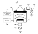
- FIG. 1 is an explanatory view showing a manufacturing process of a piezoelectric element.
- Step 1 Substrate Preparation Step First, as shown in FIG. 1A, a silicon (Si) substrate 10 is prepared.
- Step 2 Insulating Film Formation Step Next, an insulating film (for example, an oxide film such as SiO 2 ) 12 is formed on the silicon substrate 10 (FIG. 1B).
- a silicon oxide film is formed by CVD (Chemical Vapor Deposition), sputtering, vapor deposition, thermal oxidation method, or the like.
- Step 3 Lower electrode formation step Next, an adhesion layer (for example, a Ti layer) 14 is formed on the insulating film 12, and a noble metal film corresponding to the lower electrode 16 is formed on the adhesion layer 14 ( FIG. 1 (c)).
- the lower electrode 16 is made of a noble metal material such as Pt (platinum), Ir (iridium), Ru (ruthenium), or an oxide film thereof.
- the lower electrode 16 can be formed by sputtering or CVD.
- a piezoelectric body 18 is formed on the lower electrode 16.
- the piezoelectric body 18 can be formed of a ferroelectric material such as lead zirconate titanate (PZT), and can be formed by a sputtering method, a CVD method, a sol-gel method, or the like. Not only PZT but also lead lanthanum zirconate titanate (PLZT) or “PZTN” in which a part of Ti of PZT is replaced by Nb can be used as the material of the piezoelectric body 18.
- PZT lead lanthanum zirconate titanate
- Nb sol-gel method
- Step 5 Upper electrode forming step Next, a noble metal film corresponding to the upper electrode 20 is formed on the piezoelectric body 18 (FIG. 1E).
- the upper electrode 20 can be formed of Pt, Ir, Ru or an oxide film thereof (PtOx, IrOx, RuOx), and can be formed by a sputtering method or a CVD method.
- PtOx is a generic name for platinum oxide, and “x” represents a positive number indicating the ratio of Pt and O. The same applies to IrOx and RuOx.
- IrOx is a general term for oxides of iridium
- RuOx is a general term for oxides of ruthenium.
- a hard mask 22 that covers the upper electrode 20 is formed (FIG. 1F).
- the hard mask 22 can be formed using a silicon oxide film, a silicon nitride film, an organic SOG (Spin on Glass) film, an inorganic SOG film, or a metal such as Ti, Cr, Al, or Ni.
- a silicon oxide film is formed by TEOS (Tetra Ethyl Ortho Silicate) -CVD method.
- Step 7 Resist Mask Forming Step Next, a resist 24 is formed on the hard mask 22 layer by spin coating or the like, followed by soft baking, exposure and development, and then post baking. In addition, you may perform the hardening process (UV cure) by ultraviolet irradiation instead of post-baking. Thus, the resist 24 for patterning the upper electrode is patterned (FIG. 1G).
- Step 8 Hard Mask Patterning Step
- the hard mask 22 is a silicon oxide film
- the hard mask 22 is patterned by a dry etching method (FIG. 1H).
- Step 9) Resist removal step Thereafter, the resist 24 used in the patterning step of the hard mask 22 is removed using an ashing method or a special stripping solution (FIG. 1 (i)).
- Step 10 Upper electrode patterning step Patterning of the upper electrode 20 is performed by a dry etching method to which one embodiment of the present invention is applied (FIG. 1 (j)).
- the important points in dry etching of the upper electrode 20 are that the etching rate is high, the mask selection ratio and the selection ratio with the dielectric (which is PZT in this example) are high, and the etching shape is It is good. In particular, there is a problem that the base film selection ratio decreases when the etching rate is increased.
- the dry etching method according to this embodiment is a dry etching method that has a high etching rate and can sufficiently ensure a selection ratio with the base film.
- FIG. 2 is a configuration diagram of a dry etching apparatus using the dry etching method according to the present embodiment.
- the dry etching apparatus 110 for example, an inductive coupling plasma (ICP) apparatus is used.
- ICP inductive coupling plasma
- methods using plasma sources such as Helicon Wave Plasma (HWP), Electron Cyclotron Resonance (ECR) plasma, Surface Wave Plasma (SWP), etc. It is also possible to apply to the dry etching apparatus 110.
- HWP Helicon Wave Plasma
- ECR Electron Cyclotron Resonance
- SWP Surface Wave Plasma
- the dry etching apparatus 110 includes a process gas supply unit 114 that supplies a process gas (etching gas) into the chamber 112 (vacuum vessel), an exhaust unit 116 that exhausts the gas in the chamber 112, and a pressure adjustment in the chamber 112. And a pressure adjusting unit (not shown) for performing.
- the pressure in the chamber 112 is adjusted by exhausting from the exhaust unit 116 while supplying the process gas from the process gas supply unit 114 into the chamber 112.
- a mixed gas of chlorine gas and oxygen gas is used as a process gas (etching gas).
- a dielectric window 118 is hermetically attached to the upper surface of the chamber 112, and a loop coil antenna 120 is installed above the dielectric window 118 (atmosphere side).
- a high frequency power source (RF power source) 124 for generating plasma is connected to the antenna 120 via a matching circuit (matching unit) 122.
- the frequency of the high frequency power supply 124 can use a frequency band of 13.56 MHz or more and 60 MHz or less, for example, 13.56 MHz. Further, the high frequency power supply 124 may be pulse-driven.
- a stage 126 is installed in the chamber 112.
- the stage 126 is provided with a substrate cooling mechanism (not shown) provided with an electrostatic chuck or a clamp, and a substrate 128 to be etched is placed on the stage 126.
- a low frequency power supply 132 for applying a bias is connected to the stage 126 via a matching circuit 130.
- the frequency of the low frequency power supply 132 is 800 kHz or more and 4 MHz or less.
- the frequency of the low frequency power supply 132 is 900 kHz or more and 2 MHz or less.
- a frequency around 1 MHz is preferable as the frequency of the low-frequency power source 132.
- pulse driving means may be provided in the bias power source.
- the bias power source is used by pulse driving, means for synchronizing the pulse period of the power source (high frequency power source 124) of the antenna 120 (for plasma generation) and the bias power source (low frequency power source 132) is used. do it.
- the substrate (the stacked structure shown in FIG. 1 (i)) as the material to be etched is placed on the stage 126 in the chamber 112 of the dry etching apparatus 110 shown in FIG.
- the exhaust gas is exhausted by supplying the mixed gas of chlorine gas and oxygen gas as the etching gas from the process gas supply unit 114, and the inside of the chamber 112 has a predetermined gas pressure (
- the pressure is adjusted so as to be a predetermined value within a range of 1 Pa to 5 Pa, which is 3 Pa in this example.
- required power for example, 500 W power
- high-frequency power source 124 for example, 500 W power
- high-density plasma is generated in the chamber 112.
- a predetermined power for example, a power of 200 W
- the power of the antenna RF power source (high frequency power source 124) is 500 W
- the power of the bias power source (low frequency power source 132) is 200 W
- the power condition is common.
- the addition amount of oxygen gas to the chlorine gas of etching gas (mixing ratio of oxygen gas to the whole) is variable, and the etching rate of Ir and the base film are set.
- the selectivity was determined from the etching rate of PZT.
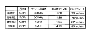
- FIG. 3 summarizes the results of Comparative Examples 1 to 3 and Examples.
- Comparative Example 1 a condition of 600 kHz was used as the frequency of the bias power source (low frequency power source 132).
- the degree of vacuum (gas pressure) in the chamber 112 was 0.5 Pa
- the oxygen flow rate ratio in the etching gas mixed gas of chlorine and oxygen
- Ir on the PZT film was etched.
- the conditions of the bias frequency and the gas pressure in Comparative Example 1 are generally used as etching conditions for noble metal materials such as Ir and Pt.
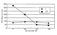
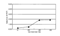
- FIG. 4 and 5 are graphs showing the results when Ir was etched under the conditions of Comparative Example 1.
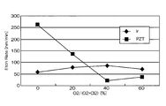
- FIG. FIG. 4 is a graph showing the relationship between the mixing ratio of oxygen gas in the mixed gas and the etching rates of Ir and PZT.
- the horizontal axis represents the mixing ratio of oxygen gas in the mixed gas of chlorine gas and oxygen gas
- the vertical axis represents the etching rate.
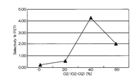
- FIG. 5 is a graph showing the relationship between the mixing ratio of oxygen gas in the mixed gas and the selection ratio (Ir / PZT).
- the horizontal axis represents the mixing ratio of oxygen gas in the mixed gas of chlorine gas and oxygen gas
- the vertical axis represents the selection ratio.
- the etching rate is relatively high as 70 to 105 nm / min, but the selection ratio with respect to PZT as the base film is 0.2 to 1
- the etching rate at that time was 75 nm / min. That is, according to the conditions of Comparative Example 1, the etching rate is as high as 75 nm / min, but the selectivity is as low as 2 or less.
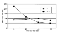
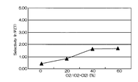
- Comparative Example 2 In Comparative Example 2, the degree of vacuum was set to 3.0 Pa, and Ir was etched under the same conditions as Comparative Example 1 except for other conditions. 6 and 7 are graphs showing the results when Ir was etched under the conditions of Comparative Example 2.
- FIG. FIG. 6 is a graph showing the relationship between the mixing ratio of oxygen gas in the mixed gas and the etching rates of Ir and PZT
- FIG. 7 shows the relationship between the mixing ratio of oxygen gas in the mixed gas and the selection ratio (Ir / PZT). It is a graph.
- the etching rate is 70 to 95 nm / min, which is relatively high, but the selectivity with respect to PZT as the base film is 0.2 to 1.
- the etching rate at that time was 75 nm / min. That is, according to the conditions of Comparative Example 2, the etching rate is as high as 75 nm / min, but the selectivity is as low as 2 or less.
- Comparative Example 3 In Comparative Example 3, the frequency of the bias power supply was set to 1 MHz, and Ir was etched under the same conditions as in Comparative Example 1 under other conditions. 8 and 9 are graphs showing the results when Ir etching was performed under the conditions of Comparative Example 3.
- FIG. FIG. 8 is a graph showing the relationship between the mixing ratio of oxygen gas in the mixed gas and the etching rates of Ir and PZT
- FIG. 9 shows the relationship between the mixing ratio of oxygen gas in the mixed gas and the selection ratio (Ir / PZT). It is a graph.
- the etching rate is relatively high, 60 to 80 nm / min, but the selection ratio with respect to PZT as the base film is 0.2 to 1.
- the etching rate at that time was 82 nm / min. That is, according to the conditions of Comparative Example 3, the etching rate is as high as 75 nm / min, but the selectivity is as low as 2 or less.
- the frequency of the bias power source is 1 MHz
- the degree of vacuum is 3.0 Pa
- a mixed gas of chlorine and oxygen is used, the flow rate ratio is changed
- the high frequency (RF) power source 500 W
- the bias (low frequency) power source Ir was etched under the condition of 200W.
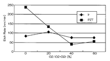
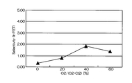
- FIG. 10 and FIG. 11 are graphs showing the results when Ir was etched under the conditions of this example.
- FIG. 10 is a graph showing the relationship between the mixing ratio of oxygen gas in the mixed gas and the etching rates of Ir and PZT
- FIG. 11 shows the relationship between the mixing ratio of oxygen gas and the selection ratio (Ir / PZT) in the mixed gas. It is a graph. As shown in FIGS.
- the etching rate is relatively high, 55 to 85 nm / min.
- the selection ratio with PZT as the base film includes a high value of about 0.2 to 4.25. The highest value was 4.25, and the etching rate at that time was 85 nm / min.
- the mixing ratio of oxygen gas when the mixing ratio of oxygen gas is in the range of 30% to 60%, a high selection ratio of 2 or more can be realized, and the Ir etching rate is also high (see FIG. 10).
- the best condition is when the mixing ratio of oxygen gas is 40%.
- the etching rate is as fast as 85 nm / min, but the selectivity is as high as 4 or more.
- Bias frequency contributes to the amount of ion energy.
- the bias frequency is lower than 800 kHz as in Comparative Example 1, the ion energy is high and the etching of the ferroelectric (PZT) as the base film proceeds, so that a sufficient selection ratio cannot be obtained.
- the bias frequency is 4 MHz or more, the ion energy is low and the noble metal material cannot be etched at high speed.
- the bias frequency is desirably 800 kHz or more and less than 4 MHz, and more desirably approximately 1 MHz.
- a range of “substantially” in the case of approximately 1 MHz an appropriate allowable range can be set within a range in which a corresponding operation effect can be obtained. For example, assuming that ⁇ 15% ( ⁇ 150 kHz) is an allowable range, approximately 1 MHz is a range of 850 kHz to 1.15 MHz, and ⁇ 10% ( ⁇ 100 kHz) is a range of 900 kHz to 1.1 MHz, Further, if ⁇ 5% ( ⁇ 50 kHz) is an allowable range, the range is 950 kHz to 1.05 MHz.
- etching pressure When the etching pressure is less than 1 Pa, the ion energy is high, the etching rate of the ferroelectric film (PZT) as the base film is fast, and a sufficient selection ratio cannot be obtained. On the other hand, when the pressure is 5 Pa or more, a large amount of radicals are generated, the amount of ions is small and the ion energy is low, and the noble metal material cannot be etched sufficiently. From the above, the etching pressure (also referred to as “processing pressure”) is preferably 1 Pa or more and less than 5 Pa, and more preferably about 3 Pa.
- an appropriate allowable range can be set within a range in which a corresponding effect can be obtained. For example, when ⁇ 0.5 Pa is an allowable range, approximately 3 Pa is a range of 3 Pa ⁇ 0.5 Pa, and ⁇ 10% is a range of 3 Pa ⁇ 0.3 Pa when an allowable range is ⁇ 10%.
- Etching gas As the etching gas, a mixed gas of chlorine and oxygen is used. In the case of only chlorine, the etching rate of the ferroelectric film (for example, PZT) which is the base film is fast and the selection ratio cannot be obtained.
- the oxidation reaction of the etchant is performed by adding oxygen gas. That is, Ir, which is a noble metal material, is oxidized to produce oxide IrOx, and the etching rate is improved.
- IrOx is a generic name for oxides of iridium, and “x” represents a positive number indicating the ratio of Ir to O.
- the etching rate of oxides such as ferroelectrics is reduced by the addition of oxygen gas.
- the effect is drastically exhibited at an oxygen addition ratio (oxygen partial pressure) of 30% or more (see FIG. 11).
- oxygen addition ratio oxygen partial pressure
- the amount of oxygen added exceeds 60%, the amount of chlorine as the main etchant decreases, and the Ir etching rate decreases.
- the addition amount (oxygen partial pressure) when adding oxygen to chlorine is 30 to 60%. More preferably, from the viewpoint of realizing a substrate selection ratio of 3 or more, the oxygen addition amount (oxygen partial pressure) is preferably 35% to 50%, and particularly preferably about 40%.
- the range of “substantially” in the case of about 40% an appropriate allowable range can be set within a range in which a corresponding action and effect can be obtained. For example, if ⁇ 5% is an allowable range, approximately 40% is in the range of 35% to 45%.
- the “substantially” range may be determined from the graph of FIG. 11 from the viewpoint of the amount of oxygen added with a selection ratio of 4 or more.
- the desired good etching result can be obtained by the combination of the bias frequency, gas pressure, and etching gas conditions described in [1] to [3] above.
- the bias frequency is about 1 MHz
- oxygen is added to chlorine as an etching gas
- the oxygen partial pressure is 40%
- the degree of vacuum is about 3 Pa
- the Ir etching rate is high and the underlying film is used.
- Etching can be performed while ensuring a sufficient selection ratio of 4 or more with PZT.
- the piezoelectric element manufactured by the process described in FIG. 1 (i) can be used for various applications such as an actuator and a sensor.
- a pressure chamber ink chamber
- a unimorph piezoelectric actuator is configured by a structure in which the lower electrode 16, the piezoelectric body 18, and the upper electrode 20 are laminated on the diaphragm. That is, FIG. 1 can be grasped as an actuator manufacturing process.
- the present invention is not limited to a unimoful type actuator, and can be applied to the manufacture of various types of actuators such as a bimorph actuator.
- the scope of application of the present invention is not limited to the piezoelectric devices exemplified above, and can be widely applied to various devices having a structure in which a dielectric and a conductive material (electrode) are laminated.
- Such devices include various devices such as capacitors, acceleration sensors, temperature sensors, memory devices, pyroelectric devices and the like.
- a dry etching method for etching a conductive material laminated on a dielectric material wherein a mixed gas containing a halogen gas and an oxygen gas is used as an etching gas, and a mixing ratio of oxygen gas in the mixed gas is 30% or more and 60%
- An etching target in which the gas pressure in the chamber when supplying the mixed gas into the chamber to generate plasma is in a range of 1 Pa to less than 5 Pa, and the conductive material is stacked on the dielectric material.
- Etching is performed by applying a bias voltage having a frequency of 800 kHz or more and less than 4 MHz as a bias voltage to the material.
- etching gas It is preferable to use a mixed gas of chlorine gas and oxygen gas as the etching gas.
- the dry etching method of this aspect is a means capable of satisfactorily etching the noble metal material in a structure in which the noble metal material is laminated on the ferroelectric material.
- PZT As the dielectric material, PZT, PLZT, or PZTN can be used.
- the conductive material is any one of Ru, Ir, and Pt, or any of RuOx, IrOx, and PtOx that is an oxide thereof.
- the dry etching method of this aspect is a means for satisfactorily etching a noble metal such as Ru, Ir, or Pt or a metal oxide thereof.
- Such an embodiment is particularly effective in that both a high etching rate and a sufficient selection ratio can be achieved.
- the electrode conductive material
- the occurrence of a shape defect or the like is suppressed.
- the device with the stable characteristic can be manufactured.
- This embodiment is an effective means for manufacturing an actuator.
- the second electrode second conductive material
- the occurrence of a shape defect or the like is suppressed.
Abstract
To increase the etching rate of a conductive material that is laminated on a dielectric material, while improving the selectivity over the dielectric material that serves as the base. A mixed gas containing a halogen gas and an oxygen gas is used as the etching gas. The mixing ratio of the oxygen gas in the mixed gas is set to 30-60% (inclusive). The gas pressure within a chamber at the time when a plasma is generated by supplying the mixed gas into the chamber is set within the range from 1 Pa (inclusive) to 5 Pa (exclusive). Etching is carried out while applying a bias voltage having a frequency of 800 kHz or more but less than 4 MHz to a material to be etched in which a conductive material is laminated on a dielectric material.
Description
本発明はドライエッチング方法及びデバイス製造方法に係り、特に誘電体材料に金属材料が積層された積層構造体における金属材料のパターニング加工に好適なドライエッチング技術、及びこれを適用してアクチュエータ、センサその他各種の回路素子などを製造するためのデバイス製造技術に関する。
The present invention relates to a dry etching method and a device manufacturing method, and in particular, a dry etching technique suitable for patterning a metal material in a laminated structure in which a metal material is laminated on a dielectric material, and an actuator, a sensor, etc. The present invention relates to a device manufacturing technique for manufacturing various circuit elements.
特許文献1は、レジストマスク(耐エッチングマスク層)を用いたドライエッチングによってイリジウム(Ir)系の導電膜、特にIrO2膜をパターニングする技術において、蒸気圧の低い反応生成物をパターンの側壁に残さず、しかも高い寸法精度で微細なパターンを形成できる方法を提案している。具体的には、レジストマスクを用いたドライエッチングで誘電体膜上のIrO2膜をパターニングする際、塩素ガスを主成分として含むとともに酸素を添加ガスとして含むエッチングガスを使用し、IrO2膜の対レジスト選択比を低下させ、レジストマスクの側壁を後退させる。これにより、パターン側壁に付着する側壁付着膜を除去する方法が提供される。
Patent Document 1 discloses a technique for patterning an iridium (Ir) -based conductive film, particularly an IrO 2 film, by dry etching using a resist mask (etching-resistant mask layer), and a reaction product having a low vapor pressure is applied to the side wall of the pattern. We have proposed a method that can form a fine pattern with high dimensional accuracy without leaving a residue. Specifically, when patterning the IrO 2 film on the dielectric film by dry etching using a resist mask, using an etching gas containing an oxygen addition gas with a chlorine-containing gas as the main component, the IrO 2 film The resist selection ratio is lowered and the side wall of the resist mask is retracted. This provides a method for removing the sidewall adhesion film adhering to the pattern sidewall.
特許文献2は、レジストマスクを用いてイリジウムの金属薄膜をパターニングするドライエッチング方法において、活性ガス及びフッ素系ガスを含有したエッチングガスを用いることを開示している。
Patent Document 2 discloses that a dry etching method of patterning an iridium metal thin film using a resist mask uses an etching gas containing an active gas and a fluorine-based gas.
特許文献3は、貴金属を含む膜のドライエッチング方法において、ハロゲンガスと不活性ガスの混合ガスをエッチング処理ガスとして、高真空、高密度プラズマ下で貴金属を含む膜に低周波のバイアス電力を印加することにより側壁付着のないドライエッチング方法を提供している。
Patent Document 3 applies a low-frequency bias power to a film containing a noble metal in a high vacuum, high-density plasma, using a mixed gas of a halogen gas and an inert gas as an etching gas in a dry etching method for a film containing a noble metal. Thus, a dry etching method without side wall adhesion is provided.
例えば、圧電素子に用いられる圧電体やその電極に用いる貴金属などは、難エッチング材料と言われ、ドライエッチングによる加工が困難である。このような材料に対し、一般的には、特許文献2、3に記載のように、ハロゲンガスや不活性ガスとの混合ガスを用いてエッチング加工が行われるが、(1)エッチング速度が遅い、(2)レジストなどのマスク選択比が低い、(3)下地膜との選択比が低いなどの課題がある。
For example, a piezoelectric body used for a piezoelectric element and a noble metal used for an electrode thereof are said to be difficult to etch materials and are difficult to process by dry etching. Such materials are generally etched using a mixed gas of halogen gas or inert gas as described in Patent Documents 2 and 3, but (1) the etching rate is slow. There are problems such as (2) low mask selection ratio of resist or the like, and (3) low selection ratio with the underlying film.
具体的な例を示すと、シリコン基板上に、絶縁膜であるシリコン酸化膜、下部電極、圧電体、及び上部電極の順に積層された積層構造を有する圧電素子の場合、この積層された上部電極をパターニングする際には、圧電体との選択比が低く、エッチングレートも遅いと言った課題がある。
As a specific example, in the case of a piezoelectric element having a laminated structure in which a silicon oxide film as an insulating film, a lower electrode, a piezoelectric body, and an upper electrode are laminated in this order on a silicon substrate, this laminated upper electrode When patterning is performed, there is a problem that the selection ratio to the piezoelectric body is low and the etching rate is slow.
しかし、特許文献1では、下地膜である誘電体との選択比に関して記載がない。特許文献1では、Irエッチング時に発光分光分析(OES:Optical Emission Spectroscopy)にてエッチングストップを行っているが、下地膜との選択比が低いと下地膜である誘電体の削り量が多くなり、形状不良が発生するという問題がある。また、誘電体層に削り込みが発生すると、デバイスの特性が劣化する。特許文献2、3においても、下地膜との選択比について言及がない。
However, in Patent Document 1, there is no description regarding the selection ratio with respect to the dielectric as a base film. In Patent Document 1, the etching is stopped by emission spectroscopic analysis (OES: Optical Emission Spectroscopy) at the time of Ir etching. There is a problem that shape defects occur. In addition, when the dielectric layer is cut, the device characteristics deteriorate. In Patent Documents 2 and 3, there is no mention of the selection ratio with the base film.
実際に本件の発明者によって実験を行ったところ、高真空の条件下でエッチャントとして塩素及び不活性ガス、若しくは塩素及び酸素を用い、低周波バイアス印加によるエッチング方法を採用して圧電体上のIrやPtなどの電極材料をエッチングした場合、下地膜である圧電体との十分な選択比が得られなかった。実験結果によれば、酸素を添加しても選択比は2程度であった。
When an experiment was actually conducted by the inventor of the present invention, it was found that chlorine and an inert gas, or chlorine and oxygen were used as etchants under high vacuum conditions, and an etching method using a low frequency bias was applied to Ir on the piezoelectric body. When an electrode material such as Pt or Pt was etched, a sufficient selection ratio with respect to the piezoelectric body as a base film could not be obtained. According to the experimental results, the selectivity was about 2 even when oxygen was added.
圧電素子に限らず、誘電体材料に金属材料が積層された構造を持つものについて、上記課題は共通する。
The above-mentioned problem is common not only for piezoelectric elements but also for a structure in which a metal material is laminated on a dielectric material.
本発明はこのような事情に鑑みてなされたものであり、金属材料とその下地となる誘電体との選択比を高めるとともに、エッチング速度(エッチングレート)の向上を達成できるドライエッチング方法及びこれを適用したデバイス製造方法を提供することを目的とする。
The present invention has been made in view of such circumstances, and a dry etching method capable of increasing the selection ratio between a metal material and a dielectric serving as a base thereof and improving the etching rate (etching rate), and An object is to provide an applied device manufacturing method.
本発明の一態様は、誘電体材料に積層された導電性材料をエッチングするドライエッチング方法であって、エッチングガスとしてハロゲンガスと酸素ガスを含む混合ガスを用い、前記混合ガスにおける酸素ガスの混合比が30%以上60%以下であり、前記混合ガスをチャンバ内に供給してプラズマを発生させる際の当該チャンバ内のガス圧を1Pa以上5Pa未満の範囲にし、前記誘電体材料に前記導電性材料が積層された被エッチング材にバイアス電圧として800kHz以上4MHz未満の周波数のバイアス電圧を印加してエッチングを行うことを特徴とするドライエッチング方法に関する。
One embodiment of the present invention is a dry etching method for etching a conductive material stacked on a dielectric material, using a mixed gas containing a halogen gas and an oxygen gas as an etching gas, and mixing the oxygen gas in the mixed gas The ratio is 30% or more and 60% or less, and when the mixed gas is supplied into the chamber to generate plasma, the gas pressure in the chamber is set in the range of 1 Pa or more and less than 5 Pa, and the dielectric material has the conductivity. The present invention relates to a dry etching method characterized in that etching is performed by applying a bias voltage having a frequency of 800 kHz or more and less than 4 MHz as a bias voltage to a material to be etched.
本発明の別の態様は、上記のドライエッチング方法を使用して前記導電性材料をエッチングによってパターニングし、当該導電性材料による電極と前記誘電体材料とが積層された構造を有するデバイスを製造することを特徴とするデバイス製造方法に関する。
According to another aspect of the present invention, the conductive material is patterned by etching using the dry etching method described above, and a device having a structure in which an electrode made of the conductive material and the dielectric material are stacked is manufactured. The present invention relates to a device manufacturing method.
本発明の別の態様は、基板上に第1の導電性材料による第1の電極を形成する第1の電極形成工程と、前記第1の電極に誘電体材料を積層する誘電体層形成工程と、前記誘電体材料の上に第2の導電性材料による第2の電極を形成する第2の電極形成工程と、前記第2の電極を構成する前記第2の導電性材料を、上記のドライエッチング方法を使用してエッチングし、前記第2の電極をパターニングするパターニング工程と、を含むことを特徴とするデバイス製造方法に関する。
Another aspect of the present invention includes a first electrode forming step of forming a first electrode made of a first conductive material on a substrate, and a dielectric layer forming step of laminating a dielectric material on the first electrode. A second electrode forming step of forming a second electrode made of a second conductive material on the dielectric material, and the second conductive material constituting the second electrode, And a patterning step of patterning the second electrode by etching using a dry etching method.
本発明の他の態様については、本明細書及び図面の記載により明らかにする。
Other aspects of the present invention will be clarified by the description of the present specification and drawings.
本発明によれば、エッチングレートが高速で、且つ、下地層である誘電体材料との選択比を確保したエッチング加工が可能である。
According to the present invention, it is possible to perform an etching process with a high etching rate and a high selection ratio with respect to the dielectric material as the underlayer.
以下、添付図面に従って本発明の実施形態について詳細に説明する。
Hereinafter, embodiments of the present invention will be described in detail with reference to the accompanying drawings.
〔圧電素子の製造プロセス例〕
ここでは、圧電素子の製造プロセスを例示し、本発明の一実施形態に係るドライエッチング方法とこれを用いた上部電極のパターニング工程を説明する。 [Example of manufacturing process of piezoelectric element]
Here, a manufacturing process of the piezoelectric element will be exemplified, and a dry etching method according to an embodiment of the present invention and an upper electrode patterning process using the dry etching method will be described.
図1は圧電素子の製造工程を示した説明図である。
FIG. 1 is an explanatory view showing a manufacturing process of a piezoelectric element.
(工程1):基板準備工程
まず、図1(a)に示すように、シリコン(Si)基板10を用意する。 (Step 1): Substrate Preparation Step First, as shown in FIG. 1A, a silicon (Si)substrate 10 is prepared.
まず、図1(a)に示すように、シリコン(Si)基板10を用意する。 (Step 1): Substrate Preparation Step First, as shown in FIG. 1A, a silicon (Si)
(工程2):絶縁膜形成工程
次に、このシリコン基板10の上に絶縁膜(例えば、SiO2などの酸化膜)12を形成する(図1(b))。一例として、CVD(Chemical Vapor Deposition:化学蒸着法)やスパッタ、蒸着、熱酸化法などによりシリコン酸化膜を形成する。 (Step 2): Insulating Film Formation Step Next, an insulating film (for example, an oxide film such as SiO 2 ) 12 is formed on the silicon substrate 10 (FIG. 1B). As an example, a silicon oxide film is formed by CVD (Chemical Vapor Deposition), sputtering, vapor deposition, thermal oxidation method, or the like.
次に、このシリコン基板10の上に絶縁膜(例えば、SiO2などの酸化膜)12を形成する(図1(b))。一例として、CVD(Chemical Vapor Deposition:化学蒸着法)やスパッタ、蒸着、熱酸化法などによりシリコン酸化膜を形成する。 (Step 2): Insulating Film Formation Step Next, an insulating film (for example, an oxide film such as SiO 2 ) 12 is formed on the silicon substrate 10 (FIG. 1B). As an example, a silicon oxide film is formed by CVD (Chemical Vapor Deposition), sputtering, vapor deposition, thermal oxidation method, or the like.
(工程3):下部電極形成工程
次いで、絶縁膜12の上に密着層(例えば、Ti層など)14を形成し、当該密着層14に重ねて下部電極16に相当する貴金属膜を形成する(図1(c))。下部電極16は、貴金属材料であるPt(白金)、Ir(イリジウム)、Ru(ルテニウム)、或いはこれらの酸化膜で形成される。下部電極16はスパッタ法やCVD法などで形成することできる。 (Step 3): Lower electrode formation step Next, an adhesion layer (for example, a Ti layer) 14 is formed on theinsulating film 12, and a noble metal film corresponding to the lower electrode 16 is formed on the adhesion layer 14 ( FIG. 1 (c)). The lower electrode 16 is made of a noble metal material such as Pt (platinum), Ir (iridium), Ru (ruthenium), or an oxide film thereof. The lower electrode 16 can be formed by sputtering or CVD.
次いで、絶縁膜12の上に密着層(例えば、Ti層など)14を形成し、当該密着層14に重ねて下部電極16に相当する貴金属膜を形成する(図1(c))。下部電極16は、貴金属材料であるPt(白金)、Ir(イリジウム)、Ru(ルテニウム)、或いはこれらの酸化膜で形成される。下部電極16はスパッタ法やCVD法などで形成することできる。 (Step 3): Lower electrode formation step Next, an adhesion layer (for example, a Ti layer) 14 is formed on the
(工程4):圧電体形成工程
次いで、図1(d)に示すように、下部電極16上へ圧電体18を形成する。圧電体18は、強誘電体であるジルコン酸チタン酸鉛(PZT)等によって形成可能であり、スパッタ法やCVD法、ゾルゲル法等で形成することができる。なお、PZTに限らず、チタン酸ジルコン酸ランタン鉛(PLZT)や、PZTのTiの一部をNbで置き換えた「PZTN」を圧電体18の材料として用いることができる。 (Step 4): Piezoelectric Forming Step Next, as shown in FIG. 1 (d), apiezoelectric body 18 is formed on the lower electrode 16. The piezoelectric body 18 can be formed of a ferroelectric material such as lead zirconate titanate (PZT), and can be formed by a sputtering method, a CVD method, a sol-gel method, or the like. Not only PZT but also lead lanthanum zirconate titanate (PLZT) or “PZTN” in which a part of Ti of PZT is replaced by Nb can be used as the material of the piezoelectric body 18.
次いで、図1(d)に示すように、下部電極16上へ圧電体18を形成する。圧電体18は、強誘電体であるジルコン酸チタン酸鉛(PZT)等によって形成可能であり、スパッタ法やCVD法、ゾルゲル法等で形成することができる。なお、PZTに限らず、チタン酸ジルコン酸ランタン鉛(PLZT)や、PZTのTiの一部をNbで置き換えた「PZTN」を圧電体18の材料として用いることができる。 (Step 4): Piezoelectric Forming Step Next, as shown in FIG. 1 (d), a
(工程5):上部電極形成工程
次に、圧電体18に重ねて上部電極20に相当する貴金属膜を形成する(図1(e))。上部電極20は、Pt、Ir、Ruやその酸化膜(PtOx、IrOx、RuOx)によって形成可能であり、スパッタ法やCVD法で形成することができる。なお、PtOxは白金の酸化物の総称であり、「x」はPtとOの比率を示す正の数を表す。IrOx及びRuOxについても同様であり、IrOxはイリジウムの酸化物の総称、RuOxはルテニウムの酸化物の総称である。 (Step 5): Upper electrode forming step Next, a noble metal film corresponding to theupper electrode 20 is formed on the piezoelectric body 18 (FIG. 1E). The upper electrode 20 can be formed of Pt, Ir, Ru or an oxide film thereof (PtOx, IrOx, RuOx), and can be formed by a sputtering method or a CVD method. PtOx is a generic name for platinum oxide, and “x” represents a positive number indicating the ratio of Pt and O. The same applies to IrOx and RuOx. IrOx is a general term for oxides of iridium, and RuOx is a general term for oxides of ruthenium.
次に、圧電体18に重ねて上部電極20に相当する貴金属膜を形成する(図1(e))。上部電極20は、Pt、Ir、Ruやその酸化膜(PtOx、IrOx、RuOx)によって形成可能であり、スパッタ法やCVD法で形成することができる。なお、PtOxは白金の酸化物の総称であり、「x」はPtとOの比率を示す正の数を表す。IrOx及びRuOxについても同様であり、IrOxはイリジウムの酸化物の総称、RuOxはルテニウムの酸化物の総称である。 (Step 5): Upper electrode forming step Next, a noble metal film corresponding to the
(工程6):ハードマスク形成工程
次に、上部電極20を覆うハードマスク22を形成する(図1(f))。ハードマスク22は、シリコン酸化膜、シリコン窒化膜、有機SOG(Spin on Glass)膜、無機SOG膜、或いはTi,Cr,Al,Niなどの金属を用いて形成可能である。ここでは、ハードマスク22として、シリコン酸化膜をTEOS(Tetra Ethyl Ortho Silicate)-CVD法で形成した。 (Step 6): Hard Mask Formation Step Next, ahard mask 22 that covers the upper electrode 20 is formed (FIG. 1F). The hard mask 22 can be formed using a silicon oxide film, a silicon nitride film, an organic SOG (Spin on Glass) film, an inorganic SOG film, or a metal such as Ti, Cr, Al, or Ni. Here, as the hard mask 22, a silicon oxide film is formed by TEOS (Tetra Ethyl Ortho Silicate) -CVD method.
次に、上部電極20を覆うハードマスク22を形成する(図1(f))。ハードマスク22は、シリコン酸化膜、シリコン窒化膜、有機SOG(Spin on Glass)膜、無機SOG膜、或いはTi,Cr,Al,Niなどの金属を用いて形成可能である。ここでは、ハードマスク22として、シリコン酸化膜をTEOS(Tetra Ethyl Ortho Silicate)-CVD法で形成した。 (Step 6): Hard Mask Formation Step Next, a
(工程7):レジストマスク形成工程
次に、ハードマスク22の層の上に、レジスト24をスピンコート法等によって形成した後、ソフトベークを行い、露光、現像を行ってからポストベークを行う。なお、ポストベークの変わりに、紫外線照射による硬化処理(UVキュア)を行っても良い。こうして、上部電極パターニング用のレジスト24がパターニングされる(図1(g))。 (Step 7): Resist Mask Forming Step Next, aresist 24 is formed on the hard mask 22 layer by spin coating or the like, followed by soft baking, exposure and development, and then post baking. In addition, you may perform the hardening process (UV cure) by ultraviolet irradiation instead of post-baking. Thus, the resist 24 for patterning the upper electrode is patterned (FIG. 1G).
次に、ハードマスク22の層の上に、レジスト24をスピンコート法等によって形成した後、ソフトベークを行い、露光、現像を行ってからポストベークを行う。なお、ポストベークの変わりに、紫外線照射による硬化処理(UVキュア)を行っても良い。こうして、上部電極パターニング用のレジスト24がパターニングされる(図1(g))。 (Step 7): Resist Mask Forming Step Next, a
(工程8):ハードマスクパターニング工程
ハードマスク22がシリコン酸化膜の場合は、ドライエッチング法でハードマスク22のパターニングを行う(図1(h))。 (Step 8): Hard Mask Patterning Step When thehard mask 22 is a silicon oxide film, the hard mask 22 is patterned by a dry etching method (FIG. 1H).
ハードマスク22がシリコン酸化膜の場合は、ドライエッチング法でハードマスク22のパターニングを行う(図1(h))。 (Step 8): Hard Mask Patterning Step When the
(工程9):レジスト除去工程
その後、上記ハードマスク22のパターニング工程で用いたレジスト24をアッシング法や専用の剥離液を用いて除去する処理を行う(図1(i))。 (Step 9): Resist removal step Thereafter, the resist 24 used in the patterning step of thehard mask 22 is removed using an ashing method or a special stripping solution (FIG. 1 (i)).
その後、上記ハードマスク22のパターニング工程で用いたレジスト24をアッシング法や専用の剥離液を用いて除去する処理を行う(図1(i))。 (Step 9): Resist removal step Thereafter, the resist 24 used in the patterning step of the
(工程10):上部電極パターニング工程
上部電極20のパターニングは、本発明の一態様を適用したドライエッチング法で行う(図1(j))。上部電極20のドライエッチングで重要な点としては、エッチングレートが高速であること、マスク選択比や下地膜である誘電体(本例ではPZTとする)との選択比が高いこと、エッチング形状が良好であること、などが挙げられる。特には、エッチングレートを高速にすると下地膜選択比が低下するという課題がある。 (Step 10): Upper electrode patterning step Patterning of theupper electrode 20 is performed by a dry etching method to which one embodiment of the present invention is applied (FIG. 1 (j)). The important points in dry etching of the upper electrode 20 are that the etching rate is high, the mask selection ratio and the selection ratio with the dielectric (which is PZT in this example) are high, and the etching shape is It is good. In particular, there is a problem that the base film selection ratio decreases when the etching rate is increased.
上部電極20のパターニングは、本発明の一態様を適用したドライエッチング法で行う(図1(j))。上部電極20のドライエッチングで重要な点としては、エッチングレートが高速であること、マスク選択比や下地膜である誘電体(本例ではPZTとする)との選択比が高いこと、エッチング形状が良好であること、などが挙げられる。特には、エッチングレートを高速にすると下地膜選択比が低下するという課題がある。 (Step 10): Upper electrode patterning step Patterning of the
以下でさらに詳述する本実施形態に係るドライエッチング方法は、エッチングレートが高速で、且つ下地膜との選択比を十分に確保することができるドライエッチング方法である。
The dry etching method according to this embodiment, which will be described in further detail below, is a dry etching method that has a high etching rate and can sufficiently ensure a selection ratio with the base film.
<ドライエッチング装置の構成例>
図2は本実施形態に係るドライエッチング方法を使用するドライエッチング装置の構成図である。ドライエッチング装置110は、例えば誘電結合方式(Inductive Coupling Plasma:ICP)の装置を用いる。その他には、ヘリコン波励起プラズマ(Helicon Wave Plasma:HWP)、電子サイクロトン共鳴(Electron Cyclotron Resonance:ECR)プラズマ、マイクロ波励起表面波プラズマ(Surface Wave Plasma:SWP)などのプラズマ源を用いた方式をドライエッチング装置110に適用することも可能である。 <Configuration example of dry etching equipment>
FIG. 2 is a configuration diagram of a dry etching apparatus using the dry etching method according to the present embodiment. As thedry etching apparatus 110, for example, an inductive coupling plasma (ICP) apparatus is used. In addition, methods using plasma sources such as Helicon Wave Plasma (HWP), Electron Cyclotron Resonance (ECR) plasma, Surface Wave Plasma (SWP), etc. It is also possible to apply to the dry etching apparatus 110.
図2は本実施形態に係るドライエッチング方法を使用するドライエッチング装置の構成図である。ドライエッチング装置110は、例えば誘電結合方式(Inductive Coupling Plasma:ICP)の装置を用いる。その他には、ヘリコン波励起プラズマ(Helicon Wave Plasma:HWP)、電子サイクロトン共鳴(Electron Cyclotron Resonance:ECR)プラズマ、マイクロ波励起表面波プラズマ(Surface Wave Plasma:SWP)などのプラズマ源を用いた方式をドライエッチング装置110に適用することも可能である。 <Configuration example of dry etching equipment>
FIG. 2 is a configuration diagram of a dry etching apparatus using the dry etching method according to the present embodiment. As the
ドライエッチング装置110は、チャンバ112(真空容器)内にプロセスガス(エッチングガス)を供給するプロセスガス供給部114と、チャンバ112内のガスを排気する排気部116と、チャンバ112内の圧力調整を行う圧力調整部(不図示)とを備える。プロセスガス供給部114からチャンバ112内にプロセスガスを供給しつつ、排気部116から排気を行うことにより、チャンバ112内の圧力調整が行われる。本発明に係る当該態様の実施に際して、プロセスガス(エッチングガス)として塩素ガスと酸素ガスの混合ガスが用いられる。
The dry etching apparatus 110 includes a process gas supply unit 114 that supplies a process gas (etching gas) into the chamber 112 (vacuum vessel), an exhaust unit 116 that exhausts the gas in the chamber 112, and a pressure adjustment in the chamber 112. And a pressure adjusting unit (not shown) for performing. The pressure in the chamber 112 is adjusted by exhausting from the exhaust unit 116 while supplying the process gas from the process gas supply unit 114 into the chamber 112. In carrying out the embodiment according to the present invention, a mixed gas of chlorine gas and oxygen gas is used as a process gas (etching gas).
チャンバ112の上面には誘電体窓118が密閉的に取り付けられており、さらに誘電体窓118の上方(大気側)にはループコイル状のアンテナ120が設置されている。アンテナ120には、マッチング回路(整合器)122を介して、プラズマ発生用の高周波電源(RF電源)124が接続されている。高周波電源124の周波数は13.56MHz以上60MHz以下の周波数帯を用いることができ、例えば13.56MHzを用いる。また、高周波電源124をパルス駆動させるようにしてもよい。
A dielectric window 118 is hermetically attached to the upper surface of the chamber 112, and a loop coil antenna 120 is installed above the dielectric window 118 (atmosphere side). A high frequency power source (RF power source) 124 for generating plasma is connected to the antenna 120 via a matching circuit (matching unit) 122. The frequency of the high frequency power supply 124 can use a frequency band of 13.56 MHz or more and 60 MHz or less, for example, 13.56 MHz. Further, the high frequency power supply 124 may be pulse-driven.
チャンバ112内にはステージ126が設置されている。このステージ126には、静電チャック又はクランプを備えた基板冷却機構(不図示)が設けられており、ステージ126上に被エッチング材となる基板128が載置される。ステージ126には、マッチング回路130を介して、バイアス印加用の低周波電源132が接続されている。低周波電源132の周波数は、800kHz以上4MHz以下を用いる。好ましくは、低周波電源132の周波数を900kHz以上2MHz以下とすることがよい。特に、1MHz前後の周波数が低周波電源132の周波数として好ましい。
A stage 126 is installed in the chamber 112. The stage 126 is provided with a substrate cooling mechanism (not shown) provided with an electrostatic chuck or a clamp, and a substrate 128 to be etched is placed on the stage 126. A low frequency power supply 132 for applying a bias is connected to the stage 126 via a matching circuit 130. The frequency of the low frequency power supply 132 is 800 kHz or more and 4 MHz or less. Preferably, the frequency of the low frequency power supply 132 is 900 kHz or more and 2 MHz or less. In particular, a frequency around 1 MHz is preferable as the frequency of the low-frequency power source 132.
また、バイアス電源をパルス駆動する場合には、バイアス電源に、パルス駆動手段を設ければ良い。さらに、バイアス電源をパルス駆動で使用する場合には、アンテナ120(プラズマ生成用)の電源(高周波電源124)とバイアス電源(低周波電源132)のパルス周期を同期させるための手段を用いるようにすればよい。
In addition, when the bias power source is pulse-driven, pulse driving means may be provided in the bias power source. Further, when the bias power source is used by pulse driving, means for synchronizing the pulse period of the power source (high frequency power source 124) of the antenna 120 (for plasma generation) and the bias power source (low frequency power source 132) is used. do it.
図2のドライエッチング装置110を用い、図1(j)で説明した上部電極20のエッチングを行う。具体的には次のようにする。すなわち、図2に示したドライエッチング装置110のチャンバ112内のステージ126上に、被エッチング材としての基板(図1(i)に示した積層構造体)を載置する。次いで、チャンバ112内を真空状態にした後、エッチングガスとして塩素ガスと酸素ガスの混合ガスをプロセスガス供給部114から供給しつつ排気部116によって排気を行い、チャンバ112内が所定のガス圧(例えば、1Pa以上5Pa以下の範囲内の所定値、本例では3Paとする。)となるように、圧力調整を行う。次に、高周波電源124から所要の電力(例えば、500Wの電力)をアンテナ120に供給し、チャンバ112内に高密度のプラズマを発生させる。このとき被エッチング材を保持するステージ126には、低周波電源132から所定電力(例えば、200Wの電力)が印加される。
2 is etched using the dry etching apparatus 110 shown in FIG. Specifically: That is, the substrate (the stacked structure shown in FIG. 1 (i)) as the material to be etched is placed on the stage 126 in the chamber 112 of the dry etching apparatus 110 shown in FIG. Next, after the inside of the chamber 112 is evacuated, the exhaust gas is exhausted by supplying the mixed gas of chlorine gas and oxygen gas as the etching gas from the process gas supply unit 114, and the inside of the chamber 112 has a predetermined gas pressure ( For example, the pressure is adjusted so as to be a predetermined value within a range of 1 Pa to 5 Pa, which is 3 Pa in this example. Next, required power (for example, 500 W power) is supplied from the high-frequency power source 124 to the antenna 120, and high-density plasma is generated in the chamber 112. At this time, a predetermined power (for example, a power of 200 W) is applied from the low frequency power supply 132 to the stage 126 that holds the material to be etched.
これにより、図1(i)で示した上部電極20の電極膜のうち、ハードマスク22で覆われていない部分がエッチングで除去され、ハードマスク22で覆われた部分を残して上部電極20がパターニングされる(図1(j))。その後、ハードマスク22を除去することにより、下部電極16、圧電体18及び上部電極20の積層構造を有する圧電素子をシリコン基板10上に形成することができる。
As a result, the portion of the electrode film of the upper electrode 20 shown in FIG. 1I that is not covered with the hard mask 22 is removed by etching, and the portion of the upper electrode 20 that is covered with the hard mask 22 is left. Patterning is performed (FIG. 1 (j)). Thereafter, by removing the hard mask 22, a piezoelectric element having a laminated structure of the lower electrode 16, the piezoelectric body 18 and the upper electrode 20 can be formed on the silicon substrate 10.
<エッチング条件について>
上部電極20のエッチングを行う時の好ましい条件を把握するため、エッチングガスにおける酸素ガスの混合比(酸素分圧)、ガス圧(真空度)、及びバイアス電源(低周波電源132)の周波数について条件を変えて実験を行った。 <About etching conditions>
In order to grasp the preferable conditions when theupper electrode 20 is etched, the oxygen gas mixture ratio (oxygen partial pressure) in the etching gas, the gas pressure (degree of vacuum), and the frequency of the bias power source (low frequency power source 132) The experiment was conducted while changing
上部電極20のエッチングを行う時の好ましい条件を把握するため、エッチングガスにおける酸素ガスの混合比(酸素分圧)、ガス圧(真空度)、及びバイアス電源(低周波電源132)の周波数について条件を変えて実験を行った。 <About etching conditions>
In order to grasp the preferable conditions when the
以下に示す比較例1~3並びに実施例においては、アンテナ用RF電源(高周波電源124)の電力を500W、バイアス用電源(低周波電源132)の電力を200Wとし、電力の条件は共通とした。そして、ガス圧とバイアス周波数の組み合わせを変えた条件の下で、エッチングガスの塩素ガスに対する酸素ガスの添加量(全体に対する酸素ガスの混合比)を可変として、Irのエッチングレートと下地膜であるPZTのエッチングレートから選択比を求めた。
In Comparative Examples 1 to 3 and Examples below, the power of the antenna RF power source (high frequency power source 124) is 500 W, the power of the bias power source (low frequency power source 132) is 200 W, and the power condition is common. . Then, under the condition that the combination of the gas pressure and the bias frequency is changed, the addition amount of oxygen gas to the chlorine gas of etching gas (mixing ratio of oxygen gas to the whole) is variable, and the etching rate of Ir and the base film are set. The selectivity was determined from the etching rate of PZT.
図3は、比較例1~3及び実施例の結果をまとめたものである。
FIG. 3 summarizes the results of Comparative Examples 1 to 3 and Examples.
<比較例1>
比較例1は、バイアス用電源(低周波電源132)の周波数として、600kHzの条件を用いた。チャンバ112内の真空度(ガス圧)は0.5Paとし、エッチングガス(塩素と酸素の混合ガス)における酸素の流量比を可変し、PZT膜上のIrをエッチングした。比較例1におけるバイアス周波数とガス圧の条件は、Ir、Ptなどの貴金属材料のエッチング条件として一般的に用いられている条件である。 <Comparative Example 1>
In Comparative Example 1, a condition of 600 kHz was used as the frequency of the bias power source (low frequency power source 132). The degree of vacuum (gas pressure) in thechamber 112 was 0.5 Pa, the oxygen flow rate ratio in the etching gas (mixed gas of chlorine and oxygen) was varied, and Ir on the PZT film was etched. The conditions of the bias frequency and the gas pressure in Comparative Example 1 are generally used as etching conditions for noble metal materials such as Ir and Pt.
比較例1は、バイアス用電源(低周波電源132)の周波数として、600kHzの条件を用いた。チャンバ112内の真空度(ガス圧)は0.5Paとし、エッチングガス(塩素と酸素の混合ガス)における酸素の流量比を可変し、PZT膜上のIrをエッチングした。比較例1におけるバイアス周波数とガス圧の条件は、Ir、Ptなどの貴金属材料のエッチング条件として一般的に用いられている条件である。 <Comparative Example 1>
In Comparative Example 1, a condition of 600 kHz was used as the frequency of the bias power source (low frequency power source 132). The degree of vacuum (gas pressure) in the
図4及び図5は、比較例1の条件でIrのエッチングを行った時の結果を示すグラフである。図4は、混合ガスにおける酸素ガスの混合比と、Ir、PZTそれぞれのエッチングレートの関係を示すグラフである。図4において横軸は、塩素ガスと酸素ガスとの混合ガスにおける酸素ガスの混合比であり、縦軸はエッチングレートである。
4 and 5 are graphs showing the results when Ir was etched under the conditions of Comparative Example 1. FIG. FIG. 4 is a graph showing the relationship between the mixing ratio of oxygen gas in the mixed gas and the etching rates of Ir and PZT. In FIG. 4, the horizontal axis represents the mixing ratio of oxygen gas in the mixed gas of chlorine gas and oxygen gas, and the vertical axis represents the etching rate.
図5は、混合ガスにおける酸素ガスの混合比と、選択比(Ir/PZT)の関係を示すグラフである。図5において横軸は、塩素ガスと酸素ガスとの混合ガスにおける酸素ガスの混合比であり、縦軸は選択比である。
FIG. 5 is a graph showing the relationship between the mixing ratio of oxygen gas in the mixed gas and the selection ratio (Ir / PZT). In FIG. 5, the horizontal axis represents the mixing ratio of oxygen gas in the mixed gas of chlorine gas and oxygen gas, and the vertical axis represents the selection ratio.
図4及び図5に示したように、比較例1の場合、エッチングレートは、70~105nm/minと比較的高速であるが、下地膜であるPZTとの選択比は、0.2~1.8程度と低く、一番高くても1.88であり、その時のエッチングレートは、75nm/minであった。すなわち、比較例1の条件によれば、エッチングレートは、75nm/minと高速であるが、選択比は2以下と低いものである。
As shown in FIGS. 4 and 5, in the case of the comparative example 1, the etching rate is relatively high as 70 to 105 nm / min, but the selection ratio with respect to PZT as the base film is 0.2 to 1 The etching rate at that time was 75 nm / min. That is, according to the conditions of Comparative Example 1, the etching rate is as high as 75 nm / min, but the selectivity is as low as 2 or less.
<比較例2>
比較例2は、真空度を3.0Paとし、他の条件は比較例1と同じ条件でIrをエッチングした。図6及び図7は、比較例2の条件でIrのエッチングを行った時の結果を示すグラフである。図6は混合ガスにおける酸素ガスの混合比とIr、PZTそれぞれのエッチングレートの関係を示すグラフであり、図7は混合ガスにおける酸素ガスの混合比と選択比(Ir/PZT)の関係を示すグラフである。 <Comparative Example 2>
In Comparative Example 2, the degree of vacuum was set to 3.0 Pa, and Ir was etched under the same conditions as Comparative Example 1 except for other conditions. 6 and 7 are graphs showing the results when Ir was etched under the conditions of Comparative Example 2. FIG. FIG. 6 is a graph showing the relationship between the mixing ratio of oxygen gas in the mixed gas and the etching rates of Ir and PZT, and FIG. 7 shows the relationship between the mixing ratio of oxygen gas in the mixed gas and the selection ratio (Ir / PZT). It is a graph.
図6及び図7に示したように、比較例2の場合、エッチングレートは、70~95nm/minと比較的高速であるが、下地膜であるPZTとの選択比は、0.2~1.8程度と低く、一番高くても1.88であり、その時のエッチングレートは、75nm/minであった。すなわち、比較例2の条件によれば、エッチングレートは、75nm/minと高速であるが、選択比は2以下と低いものである。
As shown in FIGS. 6 and 7, in the case of Comparative Example 2, the etching rate is 70 to 95 nm / min, which is relatively high, but the selectivity with respect to PZT as the base film is 0.2 to 1. The etching rate at that time was 75 nm / min. That is, according to the conditions of Comparative Example 2, the etching rate is as high as 75 nm / min, but the selectivity is as low as 2 or less.
<比較例3>
比較例3は、バイアス用電源の周波数を1MHzにし、その他の条件は、比較例1と同じ条件でIrをエッチングした。図8及び図9は、比較例3の条件でIrのエッチングを行った時の結果を示すグラフである。図8は混合ガスにおける酸素ガスの混合比とIr、PZTそれぞれのエッチングレートの関係を示すグラフであり、図9は混合ガスにおける酸素ガスの混合比と選択比(Ir/PZT)の関係を示すグラフである。 <Comparative Example 3>
In Comparative Example 3, the frequency of the bias power supply was set to 1 MHz, and Ir was etched under the same conditions as in Comparative Example 1 under other conditions. 8 and 9 are graphs showing the results when Ir etching was performed under the conditions of Comparative Example 3. FIG. FIG. 8 is a graph showing the relationship between the mixing ratio of oxygen gas in the mixed gas and the etching rates of Ir and PZT, and FIG. 9 shows the relationship between the mixing ratio of oxygen gas in the mixed gas and the selection ratio (Ir / PZT). It is a graph.
図8及び図9に示したように、比較例3の場合、エッチングレートは、60~80nm/minと比較的高速であるが、下地膜であるPZTとの選択比は、0.2~1.6程度と低く、一番高くても1.6であり、その時のエッチングレートは、82nm/minであった。すなわち、比較例3の条件によれば、エッチングレートは、75nm/minと高速であるが、選択比は、2以下と低いものである。
As shown in FIGS. 8 and 9, in the case of Comparative Example 3, the etching rate is relatively high, 60 to 80 nm / min, but the selection ratio with respect to PZT as the base film is 0.2 to 1. The etching rate at that time was 82 nm / min. That is, according to the conditions of Comparative Example 3, the etching rate is as high as 75 nm / min, but the selectivity is as low as 2 or less.
<実施例>
実施例として、バイアス用電源の周波数を1MHzにし、真空度3.0Pa、塩素と酸素の混合ガスを用い、流量比を可変し、高周波(RF)電源:500W、バイアス用(低周波)電源:200Wの条件でIrをエッチングした。図10及び図11は、この実施例による条件でIrのエッチングを行った時の結果を示すグラフである。図10は混合ガスにおける酸素ガスの混合比とIr、PZTそれぞれのエッチングレートの関係を示すグラフであり、図11は混合ガスにおける酸素ガスの混合比と選択比(Ir/PZT)の関係を示すグラフである。図10及び図11に示したように、エッチングレートは、55~85nm/minと比較的高速である。また、下地膜であるPZTとの選択比は、0.2~4.25程度と高い値を含む。一番高い値は4.25であり、その時のエッチングレートは、85nm/minであった。 <Example>
As an example, the frequency of the bias power source is 1 MHz, the degree of vacuum is 3.0 Pa, a mixed gas of chlorine and oxygen is used, the flow rate ratio is changed, the high frequency (RF) power source: 500 W, the bias (low frequency) power source: Ir was etched under the condition of 200W. FIG. 10 and FIG. 11 are graphs showing the results when Ir was etched under the conditions of this example. FIG. 10 is a graph showing the relationship between the mixing ratio of oxygen gas in the mixed gas and the etching rates of Ir and PZT, and FIG. 11 shows the relationship between the mixing ratio of oxygen gas and the selection ratio (Ir / PZT) in the mixed gas. It is a graph. As shown in FIGS. 10 and 11, the etching rate is relatively high, 55 to 85 nm / min. Further, the selection ratio with PZT as the base film includes a high value of about 0.2 to 4.25. The highest value was 4.25, and the etching rate at that time was 85 nm / min.
図11において、酸素ガスの混合比が30%~60%の範囲で、選択比2以上となる高い選択比を実現できるとともに、Irのエッチングレートも高速である(図10参照)。最も良好な条件は酸素ガスの混合比40%の時であり、この実施例の条件によれば、エッチングレートは、85nm/minと高速であるが、選択比は4以上と高い。
In FIG. 11, when the mixing ratio of oxygen gas is in the range of 30% to 60%, a high selection ratio of 2 or more can be realized, and the Ir etching rate is also high (see FIG. 10). The best condition is when the mixing ratio of oxygen gas is 40%. According to the conditions of this embodiment, the etching rate is as fast as 85 nm / min, but the selectivity is as high as 4 or more.
比較例1~3と実施例を対比するとわかるように、バイアス周波数、ガス圧、酸素ガスの混合比の条件は、それぞれを単独で調整しただけでは良好な条件を見出し難いが、これらが適切に組み合わされることで良好なエッチングを実現できる。
As can be seen by comparing Comparative Examples 1 to 3 with Examples, it is difficult to find favorable conditions for the bias frequency, gas pressure, and oxygen gas mixing ratio by adjusting each of them independently, but these are appropriate. Good etching can be realized by combining them.
<好ましいエッチング条件の考察>
[1]バイアス周波数について一般に、バイアス用電源の周波数(バイアス周波数)は、イオンのエネルギー量に寄与する。比較例1のようにバイアス周波数が800kHzよりも低いと、イオンエネルギーが高く、下地膜である強誘電体(PZT)のエッチングが進行してしまい、十分な選択比を得られない。逆に、バイアス周波数が4MHz以上となると、イオンエネルギーが低く、貴金属材料を高速にエッチングすることが出来ない。 <Consideration of preferable etching conditions>
[1] Bias frequency In general, the frequency of the bias power supply (bias frequency) contributes to the amount of ion energy. When the bias frequency is lower than 800 kHz as in Comparative Example 1, the ion energy is high and the etching of the ferroelectric (PZT) as the base film proceeds, so that a sufficient selection ratio cannot be obtained. On the contrary, when the bias frequency is 4 MHz or more, the ion energy is low and the noble metal material cannot be etched at high speed.
以上のことから、バイアス周波数は800kHz以上4MHz未満が望ましく、さらには略1MHzが望ましい。略1MHzという場合の「略」の範囲としては、相応の作用効果が得られる範囲で適宜の許容範囲を設定し得る。例えば、±15%(±150kHz)を許容範囲とすると、略1MHzは850kHz~1.15MHzの範囲であり、±10%(±100kHz)を許容範囲とすると900kHz~1.1MHzの範囲であり、また、±5%(±50kHz)を許容範囲とすると950kHz~1.05MHzの範囲である。
For these reasons, the bias frequency is desirably 800 kHz or more and less than 4 MHz, and more desirably approximately 1 MHz. As a range of “substantially” in the case of approximately 1 MHz, an appropriate allowable range can be set within a range in which a corresponding operation effect can be obtained. For example, assuming that ± 15% (± 150 kHz) is an allowable range, approximately 1 MHz is a range of 850 kHz to 1.15 MHz, and ± 10% (± 100 kHz) is a range of 900 kHz to 1.1 MHz, Further, if ± 5% (± 50 kHz) is an allowable range, the range is 950 kHz to 1.05 MHz.
[2]ガス圧(エッチング圧力)についてエッチング圧力は、1Pa未満の場合、イオンエネルギーが高く、下地膜である強誘電体(PZT)のエッチングレートが速く十分な選択比が得られない。逆に5Pa以上の場合は、ラジカルが多く生成されイオン量が少なく且つイオンエネルギーが低く、貴金属材料を十分にエッチングすることが出来ない。以上のことから、エッチング圧力(「処理圧力」とも言う。)は、1Pa以上5Pa未満であることが望ましく、さらには、略3Paが望ましい。略3Paという場合の「略」の範囲としては、相応の作用効果が得られる範囲で適宜の許容範囲を設定し得る。例えば、±0.5Paを許容範囲とすると、略3Paは3Pa±0.5Paの範囲であり、±10%を許容範囲とすると3Pa±0.3Paの範囲である。
[2] Gas pressure (etching pressure) When the etching pressure is less than 1 Pa, the ion energy is high, the etching rate of the ferroelectric film (PZT) as the base film is fast, and a sufficient selection ratio cannot be obtained. On the other hand, when the pressure is 5 Pa or more, a large amount of radicals are generated, the amount of ions is small and the ion energy is low, and the noble metal material cannot be etched sufficiently. From the above, the etching pressure (also referred to as “processing pressure”) is preferably 1 Pa or more and less than 5 Pa, and more preferably about 3 Pa. As the range of “substantially” in the case of about 3 Pa, an appropriate allowable range can be set within a range in which a corresponding effect can be obtained. For example, when ± 0.5 Pa is an allowable range, approximately 3 Pa is a range of 3 Pa ± 0.5 Pa, and ± 10% is a range of 3 Pa ± 0.3 Pa when an allowable range is ± 10%.
[3]エッチングガスについてエッチングガスは、塩素と酸素の混合ガスを用いる。塩素のみの場合、下地膜である強誘電体(例えば、PZT)のエッチングレートが速く選択比を得られない。酸素ガスを添加することでエッチャントの酸化反応が行われる。すなわち、貴金属材料であるIrは酸化され、酸化物IrOxが生成され、エッチングレートが向上する。なお、IrOxはイリジウムの酸化物の総称であり、「x」はIrとOの比率を示す正の数を表す。一方、強誘電体などの酸化物は、酸素ガスの添加によってエッチングレートが低下する。特には、酸素の添加比率(酸素分圧)30%以上でその効果が飛躍的に発揮される(図11参照)。ただし、酸素添加量が60%を超えてしまうと、メインのエッチャントである塩素量が低下し、Irのエッチングレートが低下してしまう。
[3] Etching gas As the etching gas, a mixed gas of chlorine and oxygen is used. In the case of only chlorine, the etching rate of the ferroelectric film (for example, PZT) which is the base film is fast and the selection ratio cannot be obtained. The oxidation reaction of the etchant is performed by adding oxygen gas. That is, Ir, which is a noble metal material, is oxidized to produce oxide IrOx, and the etching rate is improved. IrOx is a generic name for oxides of iridium, and “x” represents a positive number indicating the ratio of Ir to O. On the other hand, the etching rate of oxides such as ferroelectrics is reduced by the addition of oxygen gas. In particular, the effect is drastically exhibited at an oxygen addition ratio (oxygen partial pressure) of 30% or more (see FIG. 11). However, if the amount of oxygen added exceeds 60%, the amount of chlorine as the main etchant decreases, and the Ir etching rate decreases.
以上のことから塩素に酸素を添加する場合の添加量(酸素分圧)は30~60%が望ましい。より好ましくは、下地選択比3以上を実現する観点から酸素添加量(酸素分圧)は35%~50%であることが望ましく、特に、略40%が望ましい。略40%という場合の「略」の範囲としては、相応の作用効果が得られる範囲で適宜の許容範囲を設定し得る。例えば、±5%を許容範囲とすると、略40%は35%~45%の範囲である。或いはまた、図11のグラフから選択比が4以上となる酸素の添加量の観点から「略」の範囲を定めても良い。
From the above, it is desirable that the addition amount (oxygen partial pressure) when adding oxygen to chlorine is 30 to 60%. More preferably, from the viewpoint of realizing a substrate selection ratio of 3 or more, the oxygen addition amount (oxygen partial pressure) is preferably 35% to 50%, and particularly preferably about 40%. As the range of “substantially” in the case of about 40%, an appropriate allowable range can be set within a range in which a corresponding action and effect can be obtained. For example, if ± 5% is an allowable range, approximately 40% is in the range of 35% to 45%. Alternatively, the “substantially” range may be determined from the graph of FIG. 11 from the viewpoint of the amount of oxygen added with a selection ratio of 4 or more.
上記の[1]~[3]で説明したバイアス周波数、ガス圧、及びエッチングガスの条件の組み合わせによって、目的とする良好なエッチング結果が得られる。
The desired good etching result can be obtained by the combination of the bias frequency, gas pressure, and etching gas conditions described in [1] to [3] above.
特に、バイアス周波数に略1MHzを用い、エッチングガスとして塩素に酸素を添加し、その酸素分圧が40%、真空度を3Pa程度の条件とする時に、Irのエッチングレートが高速且つ下地膜であるPZTとの選択比を4以上と十分な選択比を確保したエッチング加工が可能となる。
In particular, when the bias frequency is about 1 MHz, oxygen is added to chlorine as an etching gas, the oxygen partial pressure is 40%, and the degree of vacuum is about 3 Pa, the Ir etching rate is high and the underlying film is used. Etching can be performed while ensuring a sufficient selection ratio of 4 or more with PZT.
<塩素ガス以外のガス種の利用可能性について>
上述の実施形態では、塩素ガスと酸素ガスの混合ガスを用いたが、本発明の実施に際しては、塩素ガスに代えて、他のハロゲンガスを用いることも可能である。 <Possibility of using gas types other than chlorine gas>
In the above-described embodiment, a mixed gas of chlorine gas and oxygen gas is used. However, in the practice of the present invention, other halogen gases can be used instead of chlorine gas.
<高周波電源の電力(パワー)について>
高周波電源124からアンテナ120に供給する電力として500Wを例示したが、電力の条件は、適宜変更可能である。電力の増減によって、図4、図6、図8、及び図10の各図に示したエッチングレートのグラフは、Ir、PZTともに全体的に上下にシフトする(エッチングレートの値が増減する)だけであり、電力の条件は選択比にほとんど影響しない。 <About the power of high-frequency power supply>
Although 500 W is exemplified as the power supplied from the high-frequency power source 124 to the antenna 120, the power condition can be changed as appropriate. As the power increases and decreases, the etching rate graphs shown in FIGS. 4, 6, 8, and 10 both shift up and down as a whole (the etching rate value increases or decreases). Therefore, the power condition hardly affects the selection ratio.
高周波電源124からアンテナ120に供給する電力として500Wを例示したが、電力の条件は、適宜変更可能である。電力の増減によって、図4、図6、図8、及び図10の各図に示したエッチングレートのグラフは、Ir、PZTともに全体的に上下にシフトする(エッチングレートの値が増減する)だけであり、電力の条件は選択比にほとんど影響しない。 <About the power of high-frequency power supply>
Although 500 W is exemplified as the power supplied from the high-
<圧電素子の用途について>
図1(i)で説明したプロセスで製造される圧電素子は、アクチュエータやセンサなど、様々な用途に用いることができる。例えば、インクジェットヘッドにおける液滴吐出圧力を発生させる圧電アクチュエータとして用いる場合には、図1(i)におけるシリコン基板10の層を加工することによって、圧力室(インク室)を構成することができる。シリコン基板10の一部が振動板として機能し、当該振動板に下部電極16、圧電体18、上部電極20が積層された構造によってユニモルフ圧電アクチュエータが構成される。つまり、図1はアクチュエータの製造工程として把握できる。また、本発明は、ユニモフル型のアクチュエータに限らず、バイモルフアクチュエータなど、各種方式のアクチュエータの製造にも適用することができる。 <Application of piezoelectric element>
The piezoelectric element manufactured by the process described in FIG. 1 (i) can be used for various applications such as an actuator and a sensor. For example, when used as a piezoelectric actuator for generating a droplet discharge pressure in an inkjet head, a pressure chamber (ink chamber) can be formed by processing the layer of thesilicon substrate 10 in FIG. A part of the silicon substrate 10 functions as a diaphragm, and a unimorph piezoelectric actuator is configured by a structure in which the lower electrode 16, the piezoelectric body 18, and the upper electrode 20 are laminated on the diaphragm. That is, FIG. 1 can be grasped as an actuator manufacturing process. Further, the present invention is not limited to a unimoful type actuator, and can be applied to the manufacture of various types of actuators such as a bimorph actuator.
図1(i)で説明したプロセスで製造される圧電素子は、アクチュエータやセンサなど、様々な用途に用いることができる。例えば、インクジェットヘッドにおける液滴吐出圧力を発生させる圧電アクチュエータとして用いる場合には、図1(i)におけるシリコン基板10の層を加工することによって、圧力室(インク室)を構成することができる。シリコン基板10の一部が振動板として機能し、当該振動板に下部電極16、圧電体18、上部電極20が積層された構造によってユニモルフ圧電アクチュエータが構成される。つまり、図1はアクチュエータの製造工程として把握できる。また、本発明は、ユニモフル型のアクチュエータに限らず、バイモルフアクチュエータなど、各種方式のアクチュエータの製造にも適用することができる。 <Application of piezoelectric element>
The piezoelectric element manufactured by the process described in FIG. 1 (i) can be used for various applications such as an actuator and a sensor. For example, when used as a piezoelectric actuator for generating a droplet discharge pressure in an inkjet head, a pressure chamber (ink chamber) can be formed by processing the layer of the
<各種デバイスへの応用について>
本発明の適用範囲は、上記に例示した圧電デバイスに限定されず、誘電体と導電性材料(電極)を積層した構造を持つ様々なデバイスに対して、広く適用できる。このようなデバイスには、コンデンサ、加速度センサ、温度センサ、メモリデバイス、焦電デバイスなど、各種デバイスが含まれる。 <Application to various devices>
The scope of application of the present invention is not limited to the piezoelectric devices exemplified above, and can be widely applied to various devices having a structure in which a dielectric and a conductive material (electrode) are laminated. Such devices include various devices such as capacitors, acceleration sensors, temperature sensors, memory devices, pyroelectric devices and the like.
なお、本発明は以上説明した実施形態に限定されるものではなく、本発明の技術的思想内で当該分野の通常の知識を有するものにより、多くの変形が可能である。
The present invention is not limited to the embodiment described above, and many modifications can be made by those having ordinary knowledge in the field within the technical idea of the present invention.
<付記:開示する発明の態様について>
上記に詳述した発明の実施形態についての記載から把握されるとおり、本明細書は少なくとも以下に示す発明を含む多様な技術思想の開示を含んでいる。 <Appendix: Aspects of Invention to be Presented>
As will be understood from the description of the embodiments of the invention described in detail above, the present specification includes disclosure of various technical ideas including at least the invention described below.
(態様1):
誘電体材料に積層された導電性材料をエッチングするドライエッチング方法であって、エッチングガスとしてハロゲンガスと酸素ガスを含む混合ガスを用い、前記混合ガスにおける酸素ガスの混合比が30%以上60%以下であり、前記混合ガスをチャンバ内に供給してプラズマを発生させる際の当該チャンバ内のガス圧を1Pa以上5Pa未満の範囲にし、前記誘電体材料に前記導電性材料が積層された被エッチング材にバイアス電圧として800kHz以上4MHz未満の周波数のバイアス電圧を印加してエッチングを行うことを特徴とするドライエッチング方法。 (Aspect 1):
A dry etching method for etching a conductive material laminated on a dielectric material, wherein a mixed gas containing a halogen gas and an oxygen gas is used as an etching gas, and a mixing ratio of oxygen gas in the mixed gas is 30% or more and 60% An etching target in which the gas pressure in the chamber when supplying the mixed gas into the chamber to generate plasma is in a range of 1 Pa to less than 5 Pa, and the conductive material is stacked on the dielectric material. Etching is performed by applying a bias voltage having a frequency of 800 kHz or more and less than 4 MHz as a bias voltage to the material.
この態様によれば、下地である誘電体材料との選択比を確保し、導電性材料のエッチング速度も高速にすることができる。
According to this aspect, it is possible to secure a selection ratio with the dielectric material that is the base, and to increase the etching rate of the conductive material.
(態様2):
態様1に記載のドライエッチング方法において、前記ハロゲンガスは、塩素ガスであることを特徴とするドライエッチング方法。 (Aspect 2):
2. The dry etching method according toaspect 1, wherein the halogen gas is chlorine gas.
態様1に記載のドライエッチング方法において、前記ハロゲンガスは、塩素ガスであることを特徴とするドライエッチング方法。 (Aspect 2):
2. The dry etching method according to
エッチングガスとして、塩素ガスと酸素ガスの混合ガスを用いる態様が好ましい。
It is preferable to use a mixed gas of chlorine gas and oxygen gas as the etching gas.
(態様3):
態様1又は2に記載のドライエッチング方法において、前記誘電体材料は、強誘電体材料であり、前記導電性材料は、貴金属材料であることを特徴とするドライエッチング方法。 (Aspect 3):
3. The dry etching method according toaspect 1 or 2, wherein the dielectric material is a ferroelectric material, and the conductive material is a noble metal material.
態様1又は2に記載のドライエッチング方法において、前記誘電体材料は、強誘電体材料であり、前記導電性材料は、貴金属材料であることを特徴とするドライエッチング方法。 (Aspect 3):
3. The dry etching method according to
本態様のドライエッチング方法は、強誘電体材料に貴金属材料が積層された構造において、当該貴金属材料を良好にエッチングすることができる手段である。
The dry etching method of this aspect is a means capable of satisfactorily etching the noble metal material in a structure in which the noble metal material is laminated on the ferroelectric material.
(態様4):
態様1から3のいずれかのドライエッチング方法において、前記誘電体材料は、PZT、若しくはPLZT、或いはPZTNからなることを特徴とするドライエッチング方法。 (Aspect 4):
4. The dry etching method according to any one ofaspects 1 to 3, wherein the dielectric material is made of PZT, PLZT, or PZTN.
態様1から3のいずれかのドライエッチング方法において、前記誘電体材料は、PZT、若しくはPLZT、或いはPZTNからなることを特徴とするドライエッチング方法。 (Aspect 4):
4. The dry etching method according to any one of
誘電体材料として、PZT、PLZT、PZTNを用いることができる。
As the dielectric material, PZT, PLZT, or PZTN can be used.
(態様5):
態様1から4のいずれかのドライエッチング方法において、前記導電性材料は、Ru、Ir、Ptのうちいずれかの金属材料、若しくは、それらの酸化物であるRuOx、IrOx、PtOxのうちのいずれかの金属酸化物(ただし、xは正の数を表す)、又はこれら材料の組み合わせからなることを特徴とするドライエッチング方法。 (Aspect 5):
In the dry etching method according to any one ofaspects 1 to 4, the conductive material is any one of Ru, Ir, and Pt, or any of RuOx, IrOx, and PtOx that is an oxide thereof. A dry etching method characterized by comprising a metal oxide (wherein x represents a positive number) or a combination of these materials.
態様1から4のいずれかのドライエッチング方法において、前記導電性材料は、Ru、Ir、Ptのうちいずれかの金属材料、若しくは、それらの酸化物であるRuOx、IrOx、PtOxのうちのいずれかの金属酸化物(ただし、xは正の数を表す)、又はこれら材料の組み合わせからなることを特徴とするドライエッチング方法。 (Aspect 5):
In the dry etching method according to any one of
本態様のドライエッチング方法は、Ru、Ir、Ptなどの貴金属或いはその金属酸化物を良好にエッチングすることが手段である。
The dry etching method of this aspect is a means for satisfactorily etching a noble metal such as Ru, Ir, or Pt or a metal oxide thereof.
(態様6):
態様1から5のいずれかのドライエッチング方法において、前記混合ガスにおける前記酸素ガスの混合比が40%±5%の範囲であり、前記ガス圧が3Pa±0.5Paの範囲であり、前記バイアス電圧の周波数が1MHz±100kHzの範囲であることを特徴とするドライエッチング方法。 (Aspect 6):
In the dry etching method of any one ofaspects 1 to 5, the mixing ratio of the oxygen gas in the mixed gas is in the range of 40% ± 5%, the gas pressure is in the range of 3 Pa ± 0.5 Pa, and the bias A dry etching method, wherein a voltage frequency is in a range of 1 MHz ± 100 kHz.
態様1から5のいずれかのドライエッチング方法において、前記混合ガスにおける前記酸素ガスの混合比が40%±5%の範囲であり、前記ガス圧が3Pa±0.5Paの範囲であり、前記バイアス電圧の周波数が1MHz±100kHzの範囲であることを特徴とするドライエッチング方法。 (Aspect 6):
In the dry etching method of any one of
かかる態様は、エッチングレートの高速化と十分な選択比を両立することができる点で、特に、効果的な条件である。
Such an embodiment is particularly effective in that both a high etching rate and a sufficient selection ratio can be achieved.
(態様7):
態様1から6のいずれかのドライエッチング方法を使用して前記導電性材料をエッチングによってパターニングし、当該導電性材料による電極と前記誘電体材料とが積層された構造を有するデバイスを製造することを特徴とするデバイス製造方法。 (Aspect 7):
Patterning the conductive material by etching using the dry etching method according to any one ofaspects 1 to 6, and manufacturing a device having a structure in which an electrode made of the conductive material and the dielectric material are stacked; A device manufacturing method.
態様1から6のいずれかのドライエッチング方法を使用して前記導電性材料をエッチングによってパターニングし、当該導電性材料による電極と前記誘電体材料とが積層された構造を有するデバイスを製造することを特徴とするデバイス製造方法。 (Aspect 7):
Patterning the conductive material by etching using the dry etching method according to any one of
この態様によれば、電極(導電性材料)のパターニングに際して、形状不良などの発生が抑制される。これにより、歩留まり向上を達成できるとともに、特性の安定したデバイスを製造することができる。
According to this aspect, when patterning the electrode (conductive material), the occurrence of a shape defect or the like is suppressed. Thereby, while improving a yield, the device with the stable characteristic can be manufactured.
(態様8):
態様7に記載のデバイス製造方法において、前記デバイスは、第1の電極と第2の電極の間に前記誘電体材料が介在する構造を有するアクチュエータであることを特徴とするデバイス製造方法。 (Aspect 8):
8. The device manufacturing method according to aspect 7, wherein the device is an actuator having a structure in which the dielectric material is interposed between a first electrode and a second electrode.
本態様はアクチュエータの製造方法として効果的な手段である。
This embodiment is an effective means for manufacturing an actuator.
(態様9):
基板上に第1の導電性材料による第1の電極を形成する第1の電極形成工程と、前記第1の電極に誘電体材料を積層する誘電体層形成工程と、前記誘電体材料の上に第2の導電性材料による第2の電極を形成する第2の電極形成工程と、前記第2の電極を構成する前記第2の導電性材料を、態様1から6のいずれかのドライエッチング方法を使用してエッチングし、前記第2の電極をパターニングするパターニング工程と、を含むことを特徴とするデバイス製造方法。 (Aspect 9):
A first electrode forming step of forming a first electrode of a first conductive material on a substrate; a dielectric layer forming step of stacking a dielectric material on the first electrode; and The second electrode forming step of forming the second electrode with the second conductive material and the second conductive material constituting the second electrode are dry-etched according to any one ofaspects 1 to 6. And a patterning step of patterning the second electrode by etching using the method.
基板上に第1の導電性材料による第1の電極を形成する第1の電極形成工程と、前記第1の電極に誘電体材料を積層する誘電体層形成工程と、前記誘電体材料の上に第2の導電性材料による第2の電極を形成する第2の電極形成工程と、前記第2の電極を構成する前記第2の導電性材料を、態様1から6のいずれかのドライエッチング方法を使用してエッチングし、前記第2の電極をパターニングするパターニング工程と、を含むことを特徴とするデバイス製造方法。 (Aspect 9):
A first electrode forming step of forming a first electrode of a first conductive material on a substrate; a dielectric layer forming step of stacking a dielectric material on the first electrode; and The second electrode forming step of forming the second electrode with the second conductive material and the second conductive material constituting the second electrode are dry-etched according to any one of
この態様によれば、第2の電極(第2の導電性材料)のパターニングに際して、形状不良などの発生が抑制される。これにより、歩留まり向上を達成できるとともに、特性の安定したデバイスを製造することができる。
According to this aspect, when patterning the second electrode (second conductive material), the occurrence of a shape defect or the like is suppressed. Thereby, while improving a yield, the device with the stable characteristic can be manufactured.
10…基板、16…下部電極(第1の電極、第1の導電性材料)、18…圧電体、20…上部電極(第2の電極、第2の導電性材料)、110…ドライエッチング装置、112…チャンバ、114…プロセスガス供給部、116…排気部、118…誘電体窓、120…アンテナ、124…高周波電源、126…ステージ、128…基板、132…低周波電源
DESCRIPTION OF SYMBOLS 10 ... Board | substrate, 16 ... Lower electrode (1st electrode, 1st electroconductive material), 18 ... Piezoelectric body, 20 ... Upper electrode (2nd electrode, 2nd electroconductive material), 110 ... Dry etching apparatus 112 ... Chamber, 114 ... Process gas supply unit, 116 ... Exhaust unit, 118 ... Dielectric window, 120 ... Antenna, 124 ... High frequency power source, 126 ... Stage, 128 ... Substrate, 132 ... Low frequency power source
Claims (9)
- 誘電体材料に積層された導電性材料をエッチングするドライエッチング方法であって、
エッチングガスとしてハロゲンガスと酸素ガスを含む混合ガスを用い、
前記混合ガスにおける酸素ガスの混合比が30%以上60%以下であり、
前記混合ガスをチャンバ内に供給してプラズマを発生させる際の当該チャンバ内のガス圧を1Pa以上5Pa未満の範囲にし、
前記誘電体材料に前記導電性材料が積層された被エッチング材にバイアス電圧として800kHz以上4MHz未満の周波数のバイアス電圧を印加してエッチングを行うことを特徴とするドライエッチング方法。 A dry etching method for etching a conductive material laminated on a dielectric material,
Using a mixed gas containing halogen gas and oxygen gas as an etching gas,
The mixing ratio of oxygen gas in the mixed gas is 30% or more and 60% or less,
The gas pressure in the chamber when generating the plasma by supplying the mixed gas into the chamber is in the range of 1 Pa or more and less than 5 Pa,
A dry etching method comprising performing etching by applying a bias voltage having a frequency of 800 kHz or more and less than 4 MHz as a bias voltage to an etching target material in which the conductive material is laminated on the dielectric material. - 前記ハロゲンガスは、塩素ガスであることを特徴とする請求項1に記載のドライエッチング方法。 2. The dry etching method according to claim 1, wherein the halogen gas is a chlorine gas.
- 前記誘電体材料は、強誘電体材料であり、前記導電性材料は、貴金属材料であることを特徴とする請求項1又は2に記載のドライエッチング方法。 3. The dry etching method according to claim 1, wherein the dielectric material is a ferroelectric material, and the conductive material is a noble metal material.
- 前記誘電体材料は、PZT、若しくはPLZT、或いはPZTNからなることを特徴とする請求項1から3のいずれか1項に記載のドライエッチング方法。 The dry etching method according to any one of claims 1 to 3, wherein the dielectric material is made of PZT, PLZT, or PZTN.
- 前記導電性材料は、Ru、Ir、Ptのうちいずれかの金属材料、若しくは、それらの酸化物であるRuOx、IrOx、PtOxのうちのいずれかの金属酸化物(ただし、xは正の数を表す)、又はこれら材料の組み合わせからなることを特徴とする請求項1から4のいずれか1項に記載のドライエッチング方法。 The conductive material may be any metal material of Ru, Ir, or Pt, or any metal oxide of RuOx, IrOx, or PtOx that is an oxide thereof (where x is a positive number). The dry etching method according to claim 1, wherein the dry etching method is a combination of these materials.
- 前記混合ガスにおける前記酸素ガスの混合比が40%±5%の範囲であり、
前記ガス圧が3Pa±0.5Paの範囲であり、
前記バイアス電圧の周波数が1MHz±100kHzの範囲であることを特徴とする請求項1から5のいずれか1項に記載のドライエッチング方法。 The mixing ratio of the oxygen gas in the mixed gas is in the range of 40% ± 5%;
The gas pressure is in the range of 3 Pa ± 0.5 Pa;
6. The dry etching method according to claim 1, wherein a frequency of the bias voltage is in a range of 1 MHz ± 100 kHz. - 請求項1から6のいずれか1項に記載のドライエッチング方法を使用して前記導電性材料をエッチングによってパターニングし、当該導電性材料による電極と前記誘電体材料とが積層された構造を有するデバイスを製造することを特徴とするデバイス製造方法。 A device having a structure in which the conductive material is patterned by etching using the dry etching method according to claim 1, and an electrode made of the conductive material and the dielectric material are laminated. To manufacture a device.
- 前記デバイスは、第1の電極と第2の電極の間に前記誘電体材料が介在する構造を有するアクチュエータであることを特徴とする請求項7に記載のデバイス製造方法。 The device manufacturing method according to claim 7, wherein the device is an actuator having a structure in which the dielectric material is interposed between a first electrode and a second electrode.
- 基板上に第1の導電性材料による第1の電極を形成する第1の電極形成工程と、
前記第1の電極に誘電体材料を積層する誘電体層形成工程と、
前記誘電体材料の上に第2の導電性材料による第2の電極を形成する第2の電極形成工程と、
前記第2の電極を構成する前記第2の導電性材料を、請求項1から6のいずれか1項に記載のドライエッチング方法を使用してエッチングし、前記第2の電極をパターニングするパターニング工程と、
を含むことを特徴とするデバイス製造方法。 A first electrode forming step of forming a first electrode of a first conductive material on a substrate;
A dielectric layer forming step of laminating a dielectric material on the first electrode;
A second electrode forming step of forming a second electrode of a second conductive material on the dielectric material;
A patterning step of patterning the second electrode by etching the second conductive material constituting the second electrode using the dry etching method according to any one of claims 1 to 6. When,
A device manufacturing method comprising:
Priority Applications (2)
| Application Number | Priority Date | Filing Date | Title |
|---|---|---|---|
| CN201280024495.0A CN103548122A (en) | 2011-05-20 | 2012-05-15 | Dry etching method and method for manufacturing device |
| US14/082,756 US20140076842A1 (en) | 2011-05-20 | 2013-11-18 | Dry etching method and device manufacturing method |
Applications Claiming Priority (2)
| Application Number | Priority Date | Filing Date | Title |
|---|---|---|---|
| JP2011-113627 | 2011-05-20 | ||
| JP2011113627A JP5766027B2 (en) | 2011-05-20 | 2011-05-20 | Dry etching method and device manufacturing method |
Related Child Applications (1)
| Application Number | Title | Priority Date | Filing Date |
|---|---|---|---|
| US14/082,756 Continuation US20140076842A1 (en) | 2011-05-20 | 2013-11-18 | Dry etching method and device manufacturing method |
Publications (1)
| Publication Number | Publication Date |
|---|---|
| WO2012161026A1 true WO2012161026A1 (en) | 2012-11-29 |
Family
ID=47217106
Family Applications (1)
| Application Number | Title | Priority Date | Filing Date |
|---|---|---|---|
| PCT/JP2012/062368 WO2012161026A1 (en) | 2011-05-20 | 2012-05-15 | Dry etching method and method for manufacturing device |
Country Status (4)
| Country | Link |
|---|---|
| US (1) | US20140076842A1 (en) |
| JP (1) | JP5766027B2 (en) |
| CN (1) | CN103548122A (en) |
| WO (1) | WO2012161026A1 (en) |
Families Citing this family (3)
| Publication number | Priority date | Publication date | Assignee | Title |
|---|---|---|---|---|
| JP6703979B2 (en) * | 2015-03-24 | 2020-06-03 | 住友化学株式会社 | Method for manufacturing niobate-based ferroelectric thin film element |
| JP2016184692A (en) * | 2015-03-26 | 2016-10-20 | 住友化学株式会社 | Method for manufacturing ferroelectric thin film element |
| JP6610883B2 (en) * | 2015-12-17 | 2019-11-27 | セイコーエプソン株式会社 | Piezoelectric devices for ultrasonic sensors |
Citations (5)
| Publication number | Priority date | Publication date | Assignee | Title |
|---|---|---|---|---|
| JP2002537653A (en) * | 1999-02-17 | 2002-11-05 | アプライド マテリアルズ インコーポレイテッド | Iridium etching method for anisotropic profile |
| JP2006060203A (en) * | 2004-08-20 | 2006-03-02 | Sharp Corp | Pt/PGO ETCHING PROCESS FOR USE IN FeRAM |
| JP2007266466A (en) * | 2006-03-29 | 2007-10-11 | Tokyo Electron Ltd | Plasma etching method, plasma etching apparatus, computer storage medium, and storage medium with treatment recipe stored thereon |
| JP2009231405A (en) * | 2008-03-21 | 2009-10-08 | Fujifilm Corp | Piezoelectric element, and manufacturing method thereof |
| JP2010219153A (en) * | 2009-03-13 | 2010-09-30 | Fujifilm Corp | Piezoelectric element, method of manufacturing the same, and inkjet head |
Family Cites Families (4)
| Publication number | Priority date | Publication date | Assignee | Title |
|---|---|---|---|---|
| KR100413649B1 (en) * | 1996-01-26 | 2004-04-28 | 마츠시타 덴끼 산교 가부시키가이샤 | Method of manufacturing semiconductor devices |
| JP2002009046A (en) * | 2000-06-19 | 2002-01-11 | Matsushita Electric Ind Co Ltd | Dry etching method and capacity forming method using the same |
| US6942813B2 (en) * | 2003-03-05 | 2005-09-13 | Applied Materials, Inc. | Method of etching magnetic and ferroelectric materials using a pulsed bias source |
| US7985603B2 (en) * | 2008-02-04 | 2011-07-26 | Texas Instruments Incorporated | Ferroelectric capacitor manufacturing process |
-
2011
- 2011-05-20 JP JP2011113627A patent/JP5766027B2/en active Active
-
2012
- 2012-05-15 CN CN201280024495.0A patent/CN103548122A/en active Pending
- 2012-05-15 WO PCT/JP2012/062368 patent/WO2012161026A1/en active Application Filing
-
2013
- 2013-11-18 US US14/082,756 patent/US20140076842A1/en not_active Abandoned
Patent Citations (5)
| Publication number | Priority date | Publication date | Assignee | Title |
|---|---|---|---|---|
| JP2002537653A (en) * | 1999-02-17 | 2002-11-05 | アプライド マテリアルズ インコーポレイテッド | Iridium etching method for anisotropic profile |
| JP2006060203A (en) * | 2004-08-20 | 2006-03-02 | Sharp Corp | Pt/PGO ETCHING PROCESS FOR USE IN FeRAM |
| JP2007266466A (en) * | 2006-03-29 | 2007-10-11 | Tokyo Electron Ltd | Plasma etching method, plasma etching apparatus, computer storage medium, and storage medium with treatment recipe stored thereon |
| JP2009231405A (en) * | 2008-03-21 | 2009-10-08 | Fujifilm Corp | Piezoelectric element, and manufacturing method thereof |
| JP2010219153A (en) * | 2009-03-13 | 2010-09-30 | Fujifilm Corp | Piezoelectric element, method of manufacturing the same, and inkjet head |
Also Published As
| Publication number | Publication date |
|---|---|
| CN103548122A (en) | 2014-01-29 |
| JP2012243992A (en) | 2012-12-10 |
| US20140076842A1 (en) | 2014-03-20 |
| JP5766027B2 (en) | 2015-08-19 |
Similar Documents
| Publication | Publication Date | Title |
|---|---|---|
| US8053955B2 (en) | Piezoelectric device and method of production thereof | |
| TWI667697B (en) | Substrate processing system and substrate processing method | |
| US20030077843A1 (en) | Method of etching conductive layers for capacitor and semiconductor device fabrication | |
| JP5595134B2 (en) | Dry etching apparatus and dry etching method | |
| JP5766027B2 (en) | Dry etching method and device manufacturing method | |
| JP4999185B2 (en) | Dry etching method and dry etching apparatus | |
| JP2009226660A (en) | Method for patterning by dry etching, mold used for it and method for manufacturing inkjet head | |
| WO2003012851A2 (en) | Method of etching ferroelectric layers | |
| WO2012086169A1 (en) | Method of manufacturing dielectric device and ashing method | |
| JP2006060203A (en) | Pt/PGO ETCHING PROCESS FOR USE IN FeRAM | |
| JP5733943B2 (en) | Method for manufacturing dielectric device | |
| JP2012243992A5 (en) | ||
| JP5800710B2 (en) | Method for manufacturing piezoelectric element | |
| WO2012057127A1 (en) | Method for manufacturing dielectric device | |
| JP2012114156A (en) | Method of manufacturing piezoelectric element | |
| JP2014060210A (en) | Dry etching method and method for manufacturing piezoelectric device | |
| JP4350120B2 (en) | Diamond etching method | |
| JP2011100865A (en) | Plasma processing method | |
| JP3896123B2 (en) | Manufacturing method of semiconductor device | |
| JP5731313B2 (en) | Plasma etching apparatus and dielectric device manufacturing method | |
| JPH113881A (en) | Ashing method and device | |
| JP2012156348A (en) | Dielectric device manufacturing method, and etching method | |
| JP2006294845A (en) | Dry etching method and system |
Legal Events
| Date | Code | Title | Description |
|---|---|---|---|
| 121 | Ep: the epo has been informed by wipo that ep was designated in this application |
Ref document number: 12789394 Country of ref document: EP Kind code of ref document: A1 |
|
| NENP | Non-entry into the national phase |
Ref country code: DE |
|
| 122 | Ep: pct application non-entry in european phase |
Ref document number: 12789394 Country of ref document: EP Kind code of ref document: A1 |