WO2012157362A1 - 電流検出装置 - Google Patents
電流検出装置 Download PDFInfo
- Publication number
- WO2012157362A1 WO2012157362A1 PCT/JP2012/059369 JP2012059369W WO2012157362A1 WO 2012157362 A1 WO2012157362 A1 WO 2012157362A1 JP 2012059369 W JP2012059369 W JP 2012059369W WO 2012157362 A1 WO2012157362 A1 WO 2012157362A1
- Authority
- WO
- WIPO (PCT)
- Prior art keywords
- current detection
- bus bar
- magnetic core
- detection bus
- detection device
- Prior art date
Links
Images


Classifications
-
- G—PHYSICS
- G01—MEASURING; TESTING
- G01R—MEASURING ELECTRIC VARIABLES; MEASURING MAGNETIC VARIABLES
- G01R19/00—Arrangements for measuring currents or voltages or for indicating presence or sign thereof
- G01R19/0092—Arrangements for measuring currents or voltages or for indicating presence or sign thereof measuring current only
-
- G—PHYSICS
- G01—MEASURING; TESTING
- G01R—MEASURING ELECTRIC VARIABLES; MEASURING MAGNETIC VARIABLES
- G01R15/00—Details of measuring arrangements of the types provided for in groups G01R17/00 - G01R29/00, G01R33/00 - G01R33/26 or G01R35/00
- G01R15/14—Adaptations providing voltage or current isolation, e.g. for high-voltage or high-current networks
- G01R15/20—Adaptations providing voltage or current isolation, e.g. for high-voltage or high-current networks using galvano-magnetic devices, e.g. Hall-effect devices, i.e. measuring a magnetic field via the interaction between a current and a magnetic field, e.g. magneto resistive or Hall effect devices
- G01R15/202—Adaptations providing voltage or current isolation, e.g. for high-voltage or high-current networks using galvano-magnetic devices, e.g. Hall-effect devices, i.e. measuring a magnetic field via the interaction between a current and a magnetic field, e.g. magneto resistive or Hall effect devices using Hall-effect devices
-
- G—PHYSICS
- G01—MEASURING; TESTING
- G01R—MEASURING ELECTRIC VARIABLES; MEASURING MAGNETIC VARIABLES
- G01R15/00—Details of measuring arrangements of the types provided for in groups G01R17/00 - G01R29/00, G01R33/00 - G01R33/26 or G01R35/00
- G01R15/14—Adaptations providing voltage or current isolation, e.g. for high-voltage or high-current networks
- G01R15/20—Adaptations providing voltage or current isolation, e.g. for high-voltage or high-current networks using galvano-magnetic devices, e.g. Hall-effect devices, i.e. measuring a magnetic field via the interaction between a current and a magnetic field, e.g. magneto resistive or Hall effect devices
- G01R15/207—Constructional details independent of the type of device used
-
- G—PHYSICS
- G01—MEASURING; TESTING
- G01R—MEASURING ELECTRIC VARIABLES; MEASURING MAGNETIC VARIABLES
- G01R3/00—Apparatus or processes specially adapted for the manufacture or maintenance of measuring instruments, e.g. of probe tips
-
- Y—GENERAL TAGGING OF NEW TECHNOLOGICAL DEVELOPMENTS; GENERAL TAGGING OF CROSS-SECTIONAL TECHNOLOGIES SPANNING OVER SEVERAL SECTIONS OF THE IPC; TECHNICAL SUBJECTS COVERED BY FORMER USPC CROSS-REFERENCE ART COLLECTIONS [XRACs] AND DIGESTS
- Y10—TECHNICAL SUBJECTS COVERED BY FORMER USPC
- Y10T—TECHNICAL SUBJECTS COVERED BY FORMER US CLASSIFICATION
- Y10T29/00—Metal working
- Y10T29/49—Method of mechanical manufacture
- Y10T29/49002—Electrical device making
- Y10T29/49117—Conductor or circuit manufacturing
Definitions
- a vehicle such as a hybrid vehicle or an electric vehicle is often equipped with a current detection device that detects a current flowing through a bus bar connected to a battery.
- a current detection device a magnetic proportional current detection device or a magnetic balance current detection device may be employed.
- a magnetic proportional type or magnetic balance type current detection device includes, for example, a magnetic core and a magnetoelectric conversion element as disclosed in Patent Document 1, Patent Document 2, and Patent Document 3.
- the magnetic core is a generally ring-shaped magnetic body formed in a series surrounding both sides of a hollow portion where both ends face each other through a gap portion and the bus bar passes therethrough.
- the hollow portion of the magnetic body is a space (current detection space) through which a current to be detected passes.
- the magnetic core has a structure in which a plurality of thin plate-like members made of a substantially ring-like magnetic material are laminated via an adhesive.
- the magnetic core having such a structure is referred to as a laminated type magnetic core.
- the magnetoelectric conversion element is disposed in the gap portion of the magnetic core, detects a magnetic flux that changes according to the current flowing through the bus bar disposed through the hollow portion, and outputs a detection signal of the magnetic flux as an electric signal. It is an element.
- a Hall element is usually adopted as the magnetoelectric conversion element.
- the maximum width (diameter) of the hollow portion of the magnetic core is larger than the width of the bus bar. It needs to be formed in a size.
- a wide bus bar is being adopted in order to prevent excessive heat generation of the bus bar as the current flowing through the bus bar increases.
- the laminated type magnetic core is likely to cause a dimensional error due to a positional relationship error between a plurality of plate-like members and a dimensional error of the adhesive layer. Therefore, the conventional current detection device including the laminated type magnetic core has a problem that a current detection error due to the dimensional error of the magnetic core is likely to occur.
- the smaller the size of the magnetic core the greater the influence of the dimensional error of the magnetic core, and the more serious the current detection accuracy becomes.
- the third component includes a penetrating portion that penetrates the hollow portion of the magnetic core, and a connecting end of each of the front and rear stages of the current transmission path that are connected to both sides of the penetrating portion in the direction penetrating the hollow portion
- This is a current detection bus bar which is made of a conductor formed with a terminal portion to be connected, and the width of the terminal portion is larger than the width of the hollow portion.
- the cross-sectional shape of the through portion in the current detection bus bar is similar to the contour shape of the hollow portion of the magnetic core.
- the current detection device has a configuration shown in the following (3-1).
- (3-1) In the current detection bus bar, at least one terminal portion has a flat plate shape, and the minimum width of the outline of the cross section of the penetrating portion is formed larger than the thickness of the flat plate-like terminal portion.
- the current detection device has a configuration shown in any of the following (3-2), (3-3), and (3-4).
- the current detection bus bar has the configuration shown in (3-1), and at least one of both end portions of the metal member penetrating the hollow portion of the magnetic core is pressed into another portion. It is a member having a structure crushed into a flat plate having a wider width, and the portion crushed into a flat plate forms a terminal portion.
- the current detection bus bar is a member having a structure in which at least one of both end portions of the rod-shaped metal member that penetrates the hollow portion of the magnetic core is processed to be thicker than the other portions by upsetting. The thickly processed portion constitutes the terminal portion.
- the current detection bus bar has the configuration shown in (3-1), and further has a structure in which a part of the flat metal member is folded along the notches formed on both sides thereof.
- the folded portion constitutes the through portion, and the flat plate portions on both sides of the folded portion constitute the terminal portion.
- the folded portion may be formed at a position biased toward one end side in the width direction of the terminal portion.
- the current detection device further includes the following components.
- the fourth component is made of an insulator, and the magnetic core and the current are exposed in a state where the terminal portion of the current detection bus bar and the connector electrically connected to the magnetoelectric transducer are exposed to the outside. Covers the detection bus bar penetration and magnetoelectric transducer, and holds the magnetic core, the current detection bus bar that penetrates the hollow portion, and the magnetoelectric transducer arranged in the gap without contacting each other. It is an insulating casing.
- the direction in which the current detection bus bar passes through the hollow portion of the magnetic core (current passing direction) is referred to as a first direction.
- the width direction and the thickness direction of the terminal portion connected before and after the through portion penetrating the hollow portion of the magnetic core are referred to as a second direction and a third direction, respectively.
- the through portion that penetrates the hollow portion of the magnetic core has a maximum cross-sectional contour width that is the width of the terminal portion, as compared to the terminal portion that is continuous before and after the through portion. It is formed smaller than (maximum width). That is, the outline shape of the cross-section of the penetrating portion is constricted in the second direction with respect to the terminal portion.
- a relatively small magnetic core can be employed in relation to the width of the bus bar, and the overall size of the apparatus including the magnetic core can be avoided.
- both ends of the current detection bus bar are terminal portions, the current detection bus bar in a state of penetrating through the hollow portion of the magnetic core is connected to the pre-stage and post-stage bus bars laid in advance. Is possible.
- the central portion (penetrating portion) penetrating the hollow portion of the magnetic core can be formed in a shape other than a flat plate shape, such as a rod shape such as a round bar or a square bar, or a cylindrical shape. Therefore, the penetrating portion can be formed with a larger cross-sectional area under the constraint that the maximum width is smaller than the width of the hollow portion of the magnetic core as compared with the flat bus bar. Therefore, even when a relatively small magnetic core is employed, excessive heat generation of the current detection bus bar can be prevented.
- the magnetic core is a member formed by sintering powder made of a magnetic material.
- the sintered type magnetic core is less likely to cause a dimensional error even if it is downsized. Therefore, the current detection apparatus according to the present invention is less likely to cause a current detection error due to the dimensional error of the magnetic core.
- the sintered type magnetic core is superior to the laminated type magnetic core in that the number of manufacturing steps and cost can be reduced.
- the cross-sectional shape of the through portion of the current detection bus bar is similar to the contour shape of the hollow portion of the magnetic core, the gap between the through portion and the magnetic core can be further reduced. As a result, the apparatus can be miniaturized by adopting a smaller magnetic core.
- the cross-sectional area of the conductor in the through portion is It is not significantly smaller than the cross-sectional area of the conductor. As a result, excessive heat generation in the penetrating portion can be prevented.
- the current detection bus bar is a member having a structure in which the end of the metal member penetrating the hollow portion of the magnetic core is crushed into a flat plate shape, the metal member that is not flat plate is inserted into the hollow portion of the magnetic core. After insertion into the flat plate, a flat terminal portion having a width wider than the width of the hollow portion can be formed. Therefore, it is possible to easily produce a current detection bus bar in which the width (diameter) of the cross-section of the penetrating portion is larger than the distance between both ends of the magnetic core (the height of the gap portion).
- a rod-shaped metal member or a cylindrical metal member can be considered as a metal member which is not flat shape.
- the current detection bus bar is a member having a structure in which the end of a bar-shaped metal member penetrating the hollow portion of the magnetic core is processed thicker than the other part by upsetting, the bar-shaped metal member After inserting into the hollow part of the magnetic core, a terminal part thicker than the thickness of the hollow part can be made. Therefore, it is possible to easily produce a current detection bus bar in which the width (diameter) of the cross-section of the penetrating portion is larger than the distance between both ends of the magnetic core (the height of the gap portion). Moreover, the part processed thickly becomes a terminal part connected with the front and back bus bars by forming screw holes.
- the current detection bus bar is a member having a structure in which a part of a flat metal member is folded back along cuts formed on both sides thereof, the current detection bus bar can be easily manufactured.
- the folded portion is formed at a position deviated toward one end side in the width direction of the terminal portion. In this case, even if the minimum width of the cross-sectional contour of the penetrating portion is formed larger than the height of the gap portion of the magnetic core, the penetrating portion of the current detection bus bar is inserted into the hollow portion of the magnetic core. It becomes possible to do. Details thereof will be described later.
- the magnetic core, the current detection bus bar, and the magnetoelectric conversion element are held in a predetermined positional relationship in advance by an insulating casing that covers a portion other than the portion to be exposed. The work of attaching the current detection device to the laid bus bar is facilitated.
- FIG. 3 is a three-side view of a current detection bus bar 30 provided in the current detection device 1.
- 5 is a perspective view schematically showing a manufacturing process of the current detection bus bar 30.
- FIG. 1 is a plan view of a current detection device 1.
- FIG. It is a perspective view which shows typically a mode that the electric current detection apparatus 1 is connected with the bus bar laid beforehand.
- FIG. 3 is a three-side view of a current detection bus bar 30A according to a first application example that can be employed in the current detection device 1; It is a top view of the member used as the origin of 30 A of bus bars for electric current detection.
- FIG. 1 is a plan view of a current detection device 1.
- FIG. It is a perspective view which shows typically a mode that the electric current detection apparatus 1 is connected with the bus bar laid beforehand.
- FIG. 3 is a three-side view of a current detection bus bar 30A according to a first application example that can be employed in the current detection device 1; It is a top view
- FIG. 6 is a three-side view of a current detection bus bar 30B according to a second application example that can be employed in the current detection device 1; It is a top view of the member used as the origin of current detection bus bar 30B. It is a figure which shows a mode that the bus bar for electric current detection 30B is inserted in the hollow part of a magnetic body core.
- FIG. 10 is a perspective view of a current detection bus bar 30C and a magnetic core according to a third application example that can be employed in the current detection device 1;
- FIG. 10 is a perspective view of a current detection bus bar 30D and a magnetic core according to a fourth application example that can be employed in the current detection device 1; It is sectional drawing which shows typically the manufacturing process of bus bar 30D for electric current detection.
- FIG. 10 is a perspective view of a current detection bus bar 30E and a magnetic core according to a fifth application example that can be employed in the current detection device 1; It is a perspective view which shows typically the manufacturing process of the bus bar for electric current detection which concerns on the 6th application example employable for the electric current detection apparatus.
- the current detection device 1 is a device that detects a current flowing in a bus bar that electrically connects a battery and a device such as a motor in an electric vehicle or a hybrid vehicle. As shown in FIG. 1, the current detection device 1 includes a magnetic core 10, a Hall element 20, a current detection bus bar 30, an insulating housing 40, and an electronic substrate 50.
- the magnetic core 10 has a shape in which both ends face each other via a gap portion 12 of about several millimeters and are formed in series around the periphery of the hollow portion 11.
- the magnetic core 10 has a narrow gap portion 12 but is formed in a generally annular shape.
- the magnetic core 10 in this embodiment is formed in an annular shape surrounding the circular hollow portion 11.
- the Hall element 20 is disposed in the gap portion 12 of the magnetic core 10, detects a magnetic flux that changes according to a current passing through the hollow portion 11 of the magnetic core 10, and outputs a magnetic flux detection signal as an electric signal. It is an example of a conversion element.
- the electronic board 50 is a board on which a circuit connected to the terminal 21 of the Hall element 20 and a connector 51 for connecting the circuit and other external circuits are mounted. Accordingly, the connector 51 is electrically connected to the hall element 20.
- the circuit mounted on the electronic substrate 50 is, for example, a circuit that amplifies a magnetic flux detection signal output from the Hall element 20.
- the hall element 20 is connected to an external circuit through an electronic substrate 50 including a connector 51.
- the current detection bus bar 30 is a conductor made of a metal such as copper, and is a part of the bus bar that electrically connects the battery and the electrical equipment. That is, a current to be detected flows through the current detection bus bar 30.
- the current detection bus bar 30 is a member independent of the battery-side bus bar connected in advance to the battery and the device-side bus bar connected in advance to the electrical equipment.
- the current detection bus bar 30 is connected to the other bus bars (battery side bus bar and device side bus bar) of the front stage and the rear stage where both ends thereof are laid in advance.
- the current detection bus bar 30 and the other bus bars at the front stage and the rear stage connected thereto form a current transmission path from the battery to the electrical equipment.
- the end portions of the other bus bars are an example of connection ends of conductors at the front and rear stages of the current detection bus bar 30 in the current transmission path.
- the penetrating part 31 is a part that penetrates the hollow part 11 of the magnetic core 10 along the current passing direction.
- the current passing direction is the thickness direction of the magnetic core 10, the axial direction of the cylinder when the annular magnetic core 10 is regarded as a cylinder, and further on the surface formed by the annular magnetic core 10. It is also an orthogonal direction. In each figure, the current passing direction is indicated as the X-axis direction. In the following description, the current passing direction (X-axis direction) is referred to as a first direction.
- the terminal part 32 in the present embodiment is a flat terminal part 32a.
- the penetration part 31 in the bus bar 30 for electric current detection is formed in rod shapes, such as column shape or elliptical column shape, for example.
- the width direction and the thickness direction of the flat terminal portion 32a are described as a Y-axis direction and a Z-axis direction, respectively.
- the width direction (Y-axis direction) and the thickness direction (Z-axis direction) of the flat terminal portion 32a are referred to as a second direction and a third direction, respectively.
- FIG. 3 is a perspective view schematically showing a manufacturing process of the current detection bus bar 30.
- the current detection bus bar 30 has a structure in which both end portions of a rod-shaped metal member 30X are processed.
- the minimum width of the cross-sectional contour of the rod-shaped metal member 30 ⁇ / b> X is formed to be larger than the gap height D ⁇ b> 2 that is the distance between both ends of the magnetic core 10. Since the metal member 30X shown in FIG. 3 has a cylindrical shape, the minimum width of the cross-sectional contour of the metal member 30X is the diameter of the metal member 30X.
- the current detecting bus bar 30 has a plate-like portion formed by pressing using a press machine 60 or the like in a certain range at both ends of the rod-shaped metal member 30X that penetrates the hollow portion 11 of the magnetic core 10. It is the member which has the structure crushed by. At this time, at least one of both ends of the rod-shaped metal member 30X is pressed into a flat plate shape after the rod-shaped metal member 30X is inserted into the hollow portion 11 of the magnetic core 10.
- the metal member 30X shown in FIG. 3 is a cylindrical member, and the through portion 31 of the current detection bus bar 30 manufactured by processing both ends of the metal member 30X is cylindrical.
- the rod-shaped metal member 30X has an elliptical bar shape with an elliptical cross section or a square bar shape with a rectangular cross section.
- the rod-shaped metal member 30X may have a rod shape whose cross section is a polygon other than a quadrangle.
- the cross-sectional shape of the metal member 30 ⁇ / b> X that is, the cross-sectional shape of the penetrating portion 31 is similar to the contour shape of the hollow portion 11 of the magnetic core 10.
- N is an integer of 3 or more
- the contour shape of the hollow portion 11 of the magnetic core 10 is a regular N square
- the shape of the metal member 30X is a regular N prism.
- the outline shape of the hollow part 11 of the magnetic body core 10 is circular, if the shape of the metal member 30X is a cylinder, it is suitable.
- the outline shape of the hollow part 11 of the magnetic body core 10 is an ellipse whose ratio of the major axis to the minor axis is R
- the shape of the metal member 30X is the ratio of the major axis to the minor axis in the cross section. It is suitable if is an elliptic cylinder with R.
- the width D5 of the flat terminal portion 32a is larger than the diameter D1 (maximum width) of the hollow portion 11.
- the minimum width D4 of the outline of the cross section of the penetration part 31 is formed larger than the thickness D6 of the flat terminal part 32a.
- the ratio of the vertical dimension and the horizontal dimension of the cross-sectional outline of the penetrating portion 31 is closer to 1 than the ratio of the vertical dimension and the horizontal dimension of the cross-section of the flat terminal portion 32.
- the minimum width D4 and the maximum width D3 in the outline of the cross section of the penetration part 31 are the same.
- that the ratio is close to 1 includes that the ratio is 1.
- the minimum width D4 of the contour of the cross section of the through portion 31 is formed to be larger than the gap height D2 that is the distance between both ends of the magnetic core 10.
- the width D5 of the flat terminal portion 32a is larger than the diameter D1 (maximum width) of the hollow portion 11 of the magnetic core 10. Therefore, the magnetic core 10 cannot be mounted on the through-hole 31 of the current detection bus bar 30 manufactured in advance. Accordingly, after a set of the magnetic core 10 and the current detection bus bar 30 penetrating through the hollow portion 11 of the magnetic core 10 is made, the current detection bus bar 30 is connected to the other bus bars in the front and rear stages. Connected.
- connection end of the other bus bar 9 connected to the flat terminal portion 32a has a structure as a terminal block, for example, and is formed with a screw hole 9A.
- the terminal portion 32 of the current detection bus bar 30 has other structures such as a fitting mechanism with another bus bar 9 in addition to the flat terminal portion 32a in which the through hole 32Z for screwing is formed. Is also possible.
- the insulating housing 40 is made of an insulator, and is a member that holds the magnetic core 10, the Hall element 20, the current detection bus bar 30, and the electronic substrate 50. Including.
- Each of the main body case 41 and the lid member 42 is an integrally formed member made of an insulating resin such as polyamide (PA), polypropylene (PP), polybutylene terephthalate (PBT), or ABS resin.
- the main body case 41 is formed in a box shape having an opening, and the lid member 42 is attached to the main body case 41 to close the opening of the main body case 41.
- the main body case 41 is formed with a first holding portion 43 and a second holding portion 44 that protrude on the inner surface thereof.
- the main body case 41 includes the first holding portion 43 and the second holding portion 44, the magnetic core 10, the current detection bus bar 30 penetrating the hollow portion 11, and the Hall element 20 disposed in the gap portion 12. Are held in a state where they are not in contact with each other.
- the first holding portion 43 is fitted into the gap between the magnetic core 10 and the through portion 31 of the current detection bus bar 30 that penetrates the hollow portion 11, thereby detecting the current detection of the magnetic core 10.
- the bus bars 30 are held in a state where they do not contact each other.
- the second holding portion 44 fits into the gap between the magnetic core 10 and the Hall element 20 disposed in the gap portion 12, thereby bringing the magnetic core 10 and the Hall element 20 into contact with each other. Hold in a state that does not.
- the main body case 41 and the lid member 42 are formed with slit-like terminal portion through holes 45 into which the terminal portions 32 at both ends of the current detection bus bar 30 are inserted from the inside to the outside.
- the first holding portion 43 of the main body case 41 and The second holding unit 44 holds the magnetic core 10, the Hall element 20, and the current detection bus bar 30.
- the lid member 42 is attached to the main body case 41 holding the magnetic core 10, the Hall element 20 and the current detection bus bar 30 so as to close the opening of the main body case 41 while sandwiching the electronic substrate 50. At this time, the other terminal portion 32 of the current detection bus bar 30 is passed from the inside to the outside with respect to the terminal portion through hole 45 of the lid member 42. Further, since the electronic board 50 is sandwiched between the main body case 41 and the lid member 42, the connector 51 mounted on the electronic board 50 is held in a state of being fitted into the chipped portion 46 formed in the main body case 41. Is done.
- the main body case 41 and the lid member 42 are provided with lock mechanisms 47 and 48 for holding them in a combined state.
- the lock mechanisms 47 and 48 shown in FIG. 1 include a claw portion 47 formed to project from the side surface of the main body case 41 and an annular frame portion 48 formed on the side of the lid member 42.
- FIG. 4 is a plan view of the current detection device 1 in a state where the main body case 41 and the lid member 42 are combined.
- the main body case 41 and the lid member 42 include a portion (terminal portion) in which the through hole 32 ⁇ / b> Z is formed in the terminal portion 32 of the current detection bus bar 30, and the electronic substrate 50.
- the connector 51 exposed to the outside, the magnetic core 10, the through-hole 31 of the current detection bus bar 30, and the Hall element 20 are covered and held.
- the through portion 31 is formed so that the maximum width D3 of the cross-sectional contour is smaller than the width D5 (maximum width) of the terminal portion. That is, the outline shape of the cross section of the through portion 31 is constricted in the second direction with respect to the terminal portion 32.
- the relatively small magnetic core 10 can be employed in relation to the widths of the other bus bars in the front and rear stages, and the entire apparatus including the magnetic core 10 can be downsized.
- the penetrating portion 31 penetrating the hollow portion 11 of the magnetic core 10 is formed in a shape other than a flat shape such as a round bar or a square bar. Therefore, the through-hole 31 is formed with a larger cross-sectional area under the constraint that the maximum width thereof is smaller than the diameter D1 (width) of the hollow portion 11 of the magnetic core 10 compared to the flat bus bar. be able to. Therefore, even when a relatively small magnetic core 10 is employed, excessive heat generation of the current detection bus bar 30 can be prevented.
- the gap between the penetration part 31 and the magnetic core 10 is further reduced. be able to. As a result, the apparatus can be reduced in size by adopting a smaller magnetic core 10.
- the cross-sectional shape of the through portion 31 is formed such that the minimum width D4 is larger than the thickness D6 (minimum width) of the terminal portion 32.
- the cross-sectional area of the conductor in the through portion 31 is greater than or equal to the cross-sectional area of the conductor in the terminal portion 32. Therefore, excessive heat generation in the penetration part 31 can be prevented.
- the terminal part 32 is a part in which the overall heat capacity combined with the connecting screw 8 and the other bus bar 9 pressed against each other is increased, the problem of heat generation due to the presence of the hole 32Y does not occur.
- the hollow portion 11 is inserted after the rod-shaped metal member 30X is inserted into the hollow portion 11 of the magnetic core 10.
- the flat terminal portion 32 having a width wider than the width D1 can be formed. That is, it is not necessary to pass the through portion 31 through the gap portion 12 of the magnetic core 10. Therefore, the current detection bus bar 30 in which the cross-sectional width D3 (diameter) of the bar-shaped through portion 31 is larger than the gap height D2 in the magnetic core 10 can be easily manufactured.
- the magnetic core 10, the Hall element 20, and the current detection bus bar 30 are other than the portion (terminal portion) of the through hole 32 ⁇ / b> Z of the terminal portion 32 and the connector 51 that should be exposed. Is held in a predetermined positional relationship by an insulating housing 40 covering the. Thereby, the operation
- the magnetic core 10 is a member formed by sintering powder made of a magnetic material. Unlike the laminated type magnetic core, the sintered type magnetic core 10 is less likely to cause a dimensional error even if it is downsized. Therefore, the current detection device 1 is less likely to cause a current detection error due to the dimensional error of the magnetic core 10. Further, the sintered type magnetic core 10 is superior in that the number of manufacturing steps and cost can be reduced as compared with the laminated type magnetic core.
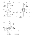
- FIG. 6 is a three-side view of the current detection bus bar 30A.
- FIG. 7 is a plan view of a flat metal member 30Y that is a source of the current detection bus bar 30A.
- the magnetic core 10 combined with the current detection bus bar 30 ⁇ / b> A is indicated by a virtual line (two-dot chain line).
- 6A is a plan view
- FIG. 6B is a side view
- FIG. 6C is a front view.
- the current detection bus bar 30 ⁇ / b> A penetrates the hollow portion 11 of the magnetic core 10 along the first direction (X-axis direction), and the current detection bus bar 30 ⁇ / b> A is It is a member made of a conductor in which flat terminal portions 32a connected to both sides in one direction are formed.
- the width D ⁇ b> 5 of the terminal portion 32 a is formed larger than the diameter D ⁇ b> 1 (maximum width) of the hollow portion 11.
- the minimum width D4 of the outline of the cross section of the penetration part 31A is formed larger than the thickness D6 of the terminal part 32a.
- the minimum width D4 of the contour of the cross section of the through portion 31A is formed smaller than the gap height D2 that is the distance between both ends of the magnetic core 10. Therefore, the magnetic core 10 can be mounted through the gap portion 12 with respect to the through portion 31A of the current detection bus bar 30A manufactured in advance.
- the portion 31Y of the flat metal member 30Y is in the second direction (Y-axis direction) along the cuts 34 formed on both sides in the first direction (X-axis direction) of the portion 31Y.
- This is a member having a structure folded from both sides.
- the notches 34 in the metal member 30Y are formed from both ends in the second direction (Y-axis direction) to the inside on both sides in the first direction (X-axis direction) of the portion 31Y.
- the folded portion 31Y constitutes the through portion 31A of the current detecting bus bar 30A, and the portions on both sides of the folded portion 31Y constitute the terminal portion 32a.
- Such a current detection bus bar 30A can be easily manufactured.
- the outline shape of the cross section of the through portion 31A is constricted in the second direction (Y-axis direction) with respect to the terminal portion 32a.
- the cross-sectional contour shape of the through portion 31A is formed such that the minimum width D4 is larger than the thickness D6 (minimum width) of the terminal portion 32a.
- the cross-sectional area of the conductor in the penetration part 31A is not significantly reduced as compared with the cross-sectional area of the conductor in the terminal part 32a.
- the cross-sectional area of the conductor in the through portion 31A and the cross-sectional area of the conductor in the terminal portion 32a are the same.
- the cross-sectional area of the conductor is smaller than the cross-sectional area of the conductors in the front and rear portions of the portion where the notch 34 is formed between the through portion 31A and the terminal portion 32a.
- the width of the notch 34 is very narrow, the increase in impedance in the portion where the notch 34 is formed is small enough to be ignored for the entire current detection bus bar 30A. .
- the narrow cut 34 is formed, excessive heat generation in the through portion 31 can be prevented.
- FIG. 8 is a three-side view of the current detection bus bar 30B.
- FIG. 9 is a plan view of a flat metal member 30Z that is the base of the current detection bus bar 30B.
- FIG. 10 is a diagram illustrating a state in which the current detection bus bar 30 ⁇ / b> B is inserted into the hollow portion 11 of the magnetic core 10.
- the magnetic core 10 combined with the current detection bus bar 30B is indicated by a virtual line (two-dot chain line).
- 8A is a plan view
- FIG. 8B is a side view
- FIG. 8C is a front view.
- the current detection bus bar 30 ⁇ / b> B has a through portion 31 ⁇ / b> B that penetrates the hollow portion 11 of the magnetic core 10 along the first direction (X-axis direction), and the second through the through portion 31 ⁇ / b> B. It is a member made of a conductor in which flat terminal portions 32a connected to both sides in one direction are formed.
- the width D5 of the terminal portion 32a is formed larger than the diameter D1 (maximum width) of the hollow portion 11.
- the minimum width D4 of the outline of the cross section of the penetration part 31B is formed larger than the thickness D6 of the terminal part 32a.
- the minimum width D4 of the cross-sectional contour of the through portion 31B is formed to be larger than the gap height D2 that is the distance between both ends of the magnetic core 10.
- the through portion 31B which is the folded portion 31Z is formed at a position biased toward one end in the second direction (Y-axis direction).
- the penetrating portion 31B is formed at a position deviated toward the positive end of the Y axis.
- the through portion 31B can be inserted into the hollow portion 11 of the magnetic core 10.
- the entire through portion 31B is positioned so as to overlap the hollow portion 11, and the terminal portion 32a is formed between the hollow portion 11 and the gap portion.
- the current detection bus bar 30 ⁇ / b> B and the magnetic core 10 are arranged so as to overlap both of the magnetic cores 10 and not to overlap the magnetic cores 10. In this state, the current detecting bus bar 30 ⁇ / b> B or the magnetic core 10 is moved in the first direction (X-axis direction), so that the penetrating portion 31 ⁇ / b> B can be inserted into the hollow portion 11 of the magnetic core 10. Therefore, it is possible to attach the magnetic core 10 to the through-hole 31B of the current detection bus bar 30B manufactured in advance.
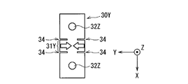
- FIG. 11 is a perspective view of the current detection bus bar 30 ⁇ / b> C and the magnetic core 10.
- FIG. 11 the same components as those shown in FIGS. 1 to 5 are given the same reference numerals.
- the differences between the current detection bus bar 30C and the current detection bus bar 30 will be described.
- the current detection bus bar 30 ⁇ / b> C has a through portion 31 that penetrates the hollow portion 11 of the magnetic core 10 along the first direction (X-axis direction), and the second through the through portion 31.
- Flat terminal portions 32a are formed on both sides in one direction.
- the two flat terminal portions 32a in the current detection bus bar 30C are formed along non-parallel surfaces.
- one of the two plate-like terminal portions 32a is formed along the XY plane, and the other is formed along the XZ plane.
- a current detection bus bar 30 ⁇ / b> C as shown in FIG. 11 may be employed instead of the current detection bus bar 30.
- the adoption of the current detection bus bar 30C shown in FIG. 11 is suitable when the angles of the surfaces formed by the front and rear bus bars are different.
- the two flat terminal portions 32a are formed along two planes intersecting each other at 90 ° as shown in FIG. 11, and along each of two planes intersecting at other angles. It is also possible that it is formed.
- the current detection bus bar 30D is different from the current detection bus bars 30 and 30A in the shape of the terminal portions 32 at both ends.
- the terminal portion 32 in the current detection bus bar 30D is a portion that is processed to be thicker than the other portions by the upsetting process at the end of the rod-shaped metal member 30X.
- the terminal portion 32 processed in this way is referred to as a large-diameter terminal portion 32b.
- the large-diameter terminal portion 32b is formed with a screw hole 32Y into which a screw 8 for coupling with a connection end of another bus bar at the front stage and the rear stage is fastened.
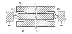
- FIG. 13 is a perspective view schematically showing a manufacturing process of the current detection bus bar 30D.
- the current detection bus bar 30 ⁇ / b> D has a structure in which both end portions of the rod-shaped metal member 30 ⁇ / b> X are processed.
- the minimum width of the cross-sectional contour of the rod-shaped metal member 30 ⁇ / b> X is formed to be larger than the gap height D ⁇ b> 2 that is the distance between both ends of the magnetic core 10.
- the large-diameter terminal portion 32b in the current detection bus bar 30D is a mold in which the end portion of the rod-shaped metal member 30X that penetrates the hollow portion 11 of the magnetic core 10 forms the large-diameter terminal portion 32b.
- This is a portion formed by upsetting using a jig 61 in which the frame portion 61z is formed, a press machine 60, and the like.
- the jig 61 holds portions other than the end portions of the rod-shaped metal member 30X along the original shape. Moreover, the mold part 61z of the jig 61 surrounds the periphery of the end part of the rod-shaped metal member 30X with an interval. And the edge part of the rod-shaped metal member 30X hold
- the process of manufacturing the current detection bus bar 30 is executed by the following procedure, for example.
- a penetrating step for penetrating the rod-shaped metal member 30X through the hollow portion 11 of the magnetic core 10 is executed.
- a first upsetting process is performed in which one end of the rod-shaped metal member 30X is processed to be thicker than the other part by the press machine 60, the jig 61, and the like.
- a second upsetting process is performed in which the other end of the rod-shaped metal member 30X is processed to be thicker than the other parts by the press machine 60, the jig 61, and the like.
- the [1] penetration process is performed before one or both of the [2] first upsetting process and the [3] second upsetting process are performed. That's fine. For example, first, [1] the penetration process may be performed, and then [2] the first upsetting process and [3] the second upsetting process may be performed simultaneously. In addition, first, [2] the first upsetting process may be performed, then [1] the penetration process may be performed, and finally [3] the second upsetting process may be performed. .
- both end portions processed to be thicker than other portions constitute a large-diameter terminal portion 32b in the current detection bus bar 30D, and a rod-shaped portion between them forms the through portion 31 of the current detection bus bar 30D.
- the metal member 30X that is the base of the current detection bus bar 30D shown in FIG. 12 is a cylindrical member, and the through-hole 31 of the current detection bus bar 30D manufactured by processing both ends of the metal member 30X is a circle. It is columnar. It should be noted that the rod-shaped metal member 30X that is the base of the current detection bus bar 30D may also be an elliptical bar having an elliptical cross section or a bar having a polygonal cross section, as in the case of the current detection bus bars 30 and 30A. It is done.
- the maximum width D5 of the large-diameter terminal portion 32b shown in FIG. 12 is formed larger than the maximum width D3 of the through portion 31 and the diameter D1 (maximum width) of the hollow portion 11.
- the thickness of the penetration part 31, ie, the thickness of the original rod-shaped metal member 30X does not have to be sufficient to form the screw hole 32Y.
- a current detection bus bar 30 ⁇ / b> D as shown in FIG. 12 may be employed instead of the current detection bus bar 30.
- FIG. 14 is a perspective view of the current detection bus bar 30 ⁇ / b> E and the magnetic core 10.
- the same components as those shown in FIGS. 1 to 12 are given the same reference numerals.
- the difference between the current detection bus bar 30E and the current detection bus bar 30D will be described.
- the current detection bus bar 30 ⁇ / b> E has a through portion 31 that penetrates the hollow portion 11 of the magnetic core 10 along the first direction (X-axis direction), and the second through the through portion 31. Large-diameter terminal portions 32b are formed on both sides in one direction.
- the current detection bus bar 30E has a bent portion 33 formed in the middle of the through portion 31 and the large-diameter terminal portion 32b.
- the current detection bus bar 30E shown in FIG. 14 is formed with a bent portion 33 that bends by 90 ° in the middle portion from the penetrating portion 31 to the large-diameter terminal portion 32b.
- a current detection bus bar 30 ⁇ / b> E as shown in FIG. 14 may be employed instead of the current detection bus bar 30.
- the adoption of the current detection bus bar 30E shown in FIG. 14 is suitable when the angles of the surfaces formed by the front and rear bus bars are different.
- the bending angle of the bending part 33 is also considered to be other bending angles besides 90 degrees as FIG. 14 shows.
- a current detection bus bar 30 ⁇ / b> E as shown in FIG. 14 may be employed instead of the current detection bus bar 30. It is also conceivable that the current detection bus bars 30 and 30A have the same bent portion 33 as the current detection bus bar 30E.
- the current detection bus bars 30A, 30B, 30C, 30D, and 30E described above do not come into contact with each other by the insulating housing 40 together with the magnetic core 10 and the hall element 20, similarly to the current detection bus bar 30. Held in a state. However, when the current detection bus bars 30B, 30C, 30D, and 30E are employed, the position or shape of the terminal portion through hole 45 of the insulating housing 40 is different from that when the current detection bus bar 30 is employed. .
- a portion of a certain range at both ends of the cylindrical metal member 30V that penetrates the hollow portion 11 of the magnetic core 10 uses the press machine 60 or the like. It is a member having a structure crushed into a flat plate shape by press working. At that time, at least one of both ends of the cylindrical metal member 30 ⁇ / b> V is pressed into a flat plate shape after the cylindrical metal member 30 ⁇ / b> V is inserted into the hollow portion 11 of the magnetic core 10.
- the current detection bus bar according to the sixth application example is held in a state of not being in contact with each other by the insulating housing 40 together with the magnetic core 10 and the hall element 20, similarly to the current detection bus bar 30.
- the metal member 30V shown in FIG. 15 is a cylindrical member, and the through-hole 31 of the current detection bus bar manufactured by processing both ends of the metal member 30V is cylindrical.
- the cylindrical metal member 30V may be an elliptic cylinder having an elliptical cross section or a square cylinder having a rectangular cross section.
- the cylindrical metal member 30V has a cylindrical shape whose cross section is a polygon other than a quadrangle.
- the cross-sectional shape of the metal member 30V that is, the cross-sectional shape of the through portion 31 in the current detection bus bar according to the sixth application example is similar to the contour shape of the hollow portion 11 of the magnetic core 10.
- the current detection bus bar 30E as shown in FIG. 14 is employed instead of the current detection bus bar 30, the same effect as that when the current detection bus bar 30 is employed is obtained. It is done.
- the flat terminal portion 32a shown in FIG. 1 or 11 is adopted as one terminal portion 32, and the large-diameter terminal portion 32b shown in FIG. 12 or FIG. It is conceivable that the other terminal portion 32 is adopted.
Landscapes
- Physics & Mathematics (AREA)
- General Physics & Mathematics (AREA)
- Measuring Instrument Details And Bridges, And Automatic Balancing Devices (AREA)
Abstract
Description
(1)第1の構成要素は、磁性材料からなる粉体の焼結により成形された部材であり、両端がギャップ部を介して対向し、中空部の周囲を囲んで一連に形成された磁性体コアである。
(2)第2の構成要素は、磁性体コアのギャップ部に配置され、磁性体コアの中空部を通過する電流に応じて変化する磁束を検出する磁電変換素子である。
(3)第3の構成要素は、磁性体コアの中空部を貫通する貫通部とその貫通部に対し中空部を貫通する方向の両側各々に連なり電流伝送経路の前段及び後段各々の接続端と連結される端子部とが形成された導体からなり、端子部の幅が中空部の幅よりも大きく形成された電流検出用バスバーである。
(3-1)電流検出用バスバーにおいて、少なくとも一方の端子部は平板状であり、貫通部の断面の輪郭の最小幅が平板状の端子部の厚みよりも大きく形成されている。
(3-2)電流検出用バスバーは、(3-1)に示される構成を有し、さらに、磁性体コアの中空部を貫通する金属部材における両端部分の少なくとも一方がプレス加工により他の部分よりも広い幅の平板状に押しつぶされた構造を有する部材であり、平板状に押しつぶされた部分が端子部を構成する。
(3-3)電流検出用バスバーは、磁性体コアの中空部を貫通する棒状の金属部材における両端部分の少なくとも一方が据え込み加工により他の部分よりも太く加工された構造を有する部材であり、太く加工された部分が端子部を構成する。
(3-4)電流検出用バスバーは、(3-1)に示される構成を有し、さらに、平板状の金属部材の一部分が、その両側に形成された切り込みに沿って折り返された構造を有する部材であり、折り返された部分が貫通部を構成し、折り返された部分の両側の平板状の部分が端子部を構成する。
(4)第4の構成要素は、絶縁体からなり、電流検出用バスバーの端子部と磁電変換素子に対して電気的に接続されたコネクタとが外部に露出する状態で、磁性体コアと電流検出用バスバーの貫通部と磁電変換素子とを覆うとともに、磁性体コアと中空部を貫通する電流検出用バスバーとギャップ部に配置された磁電変換素子とを、それらが相互に接触しない状態で保持する絶縁筐体である。
磁性体コア10は、パーマロイ、フェライト又はケイ素鋼などの磁性材料からなる粉体の焼結により成形された部材(磁性体)である。即ち、磁性体コア10は、磁性材料からなる固体粉末の集合体が、型枠内で圧縮され、さらに、その磁性体材料の融点よりも低い温度で加熱されることによって固化及び成形された部材である。
ホール素子20は、磁性体コア10のギャップ部12に配置され、磁性体コア10の中空部11を通過する電流に応じて変化する磁束を検出し、磁束の検出信号を電気信号として出力する磁電変換素子の一例である。
電子基板50は、ホール素子20の端子21に接続される回路と、その回路と外部の他の回路とを接続するコネクタ51とが実装された基板である。従って、コネクタ51は、ホール素子20に対して電気的に接続されている。電子基板50に実装された回路は、例えば、ホール素子20から出力される磁束の検出信号を増幅する回路などである。ホール素子20は、コネクタ51を含む電子基板50を介して、外部の回路と接続される。
電流検出用バスバー30は、銅などの金属からなる導電体であり、バッテリと電装機器とを電気的に接続するバスバーの一部である。即ち、電流検出用バスバー30には、検出対象の電流が流れる。また、電流検出用バスバー30は、バッテリに対して予め接続されたバッテリ側のバスバーと、電装機器に対して予め接続された機器側のバスバーとは独立した部材である。そして、電流検出用バスバー30は、その両端が予め敷設された前段及び後段の他のバスバー(バッテリ側のバスバー及び機器側のバスバー)に対して連結される。電流検出用バスバー30と、これに連結された前段及び後段の他のバスバーとは、バッテリから電装機器へ至る電流伝送経路を形成する。なお、他のバスバーの端部は、電流伝送経路における電流検出用バスバー30の前段及び後段の導体の接続端の一例である。
絶縁筐体40は、絶縁体からなり、磁性体コア10とホール素子20と電流検出用バスバー30と電子基板50とを保持する部材であり、本体ケース41及び本体ケース41に取り付けられる蓋部材42とを含む。本体ケース41及び蓋部材42の各々は、例えば、ポリアミド(PA)、ポリプロピレン(PP)、ポリブチレンテレフタレート(PBT)又はABS樹脂などの絶縁性の樹脂からなる一体成形部材である。
以上に示した電流検出装置1の電流検出用バスバー30において、貫通部31は、断面の輪郭の最大幅D3が端子部の幅D5(最大幅)よりも小さく形成されている。即ち、貫通部31の断面の輪郭形状は、端子部32に対し、第2方向においてくびれた形状を有している。その結果、電流検出装置1においては、前段及び後段の他のバスバーの幅との関係において比較的小さな磁性体コア10を採用することができ、磁性体コア10を含む装置全体を小型化できる。
次に、図6及び図7を参照しつつ、電流検出装置1に採用可能な第1応用例に係る電流検出用バスバー30Aについて説明する。図6は、電流検出用バスバー30Aの三面図である。また、図7は、電流検出用バスバー30Aの元となる平板状の金属部材30Yの平面図である。なお、図6において、電流検出用バスバー30Aと組み合わされる磁性体コア10が、仮想線(二点鎖線)により示されている。また、図6(a)は平面図、図6(b)は側面図、図6(c)は正面図である。
次に、図8~図10を参照しつつ、電流検出装置1に採用可能な第2応用例に係る電流検出用バスバー30Bについて説明する。図8は、電流検出用バスバー30Bの三面図である。また、図9は、電流検出用バスバー30Bの元となる平板状の金属部材30Zの平面図である。また、図10は、電流検出用バスバー30Bが磁性体コア10の中空部11に挿入される様子を示す図である。なお、図8において、電流検出用バスバー30Bと組み合わされる磁性体コア10が、仮想線(二点鎖線)により示されている。また、図8(a)は平面図、図8(b)は側面図、図8(c)は正面図である。
次に、図11を参照しつつ、電流検出装置1に採用可能な第3応用例に係る電流検出用バスバー30Cについて説明する。図11は、電流検出用バスバー30C及び磁性体コア10の斜視図である。図11において、図1~図5に示される構成要素と同じ構成要素は、同じ参照符号が付されている。以下、電流検出用バスバー30Cにおける電流検出用バスバー30と異なる点についてのみ説明する。
次に、図12を参照しつつ、電流検出装置1に採用可能な第4応用例に係る電流検出用バスバー30Dについて説明する。図12は、電流検出用バスバー30D及び磁性体コア10の斜視図である。図12において、図1~図5に示される構成要素と同じ構成要素は、同じ参照符号が付されている。以下、電流検出用バスバー30Dにおける電流検出用バスバー30と異なる点についてのみ説明する。
次に、図14を参照しつつ、電流検出装置1に採用可能な第5応用例に係る電流検出用バスバー30Eについて説明する。図14は、電流検出用バスバー30E及び磁性体コア10の斜視図である。図14において、図1~図12に示される構成要素と同じ構成要素は、同じ参照符号が付されている。以下、電流検出用バスバー30Eにおける電流検出用バスバー30Dと異なる点についてのみ説明する。
次に、図15を参照しつつ、電流検出装置1に採用可能な第6応用例に係る電流検出用バスバーについて説明する。図15は、第6応用例に係る電流検出用バスバー30の製造工程を模式的に示す斜視図である。図15において、図1~図3に示される構成要素と同じ構成要素は、同じ参照符号が付されている。以下、第6応用例に係る電流検出用バスバーにおける電流検出用バスバー30と異なる点についてのみ説明する。
電流検出装置1の電流検出用バスバーにおいて、図1又は図11に示される平板状の端子部32aが一方の端子部32として採用され、図12又は図14に示される大径の端子部32bが他方の端子部32として採用されることも考えられる。
8 ネジ
9 他のバスバー
9A 孔
10 磁性体コア
11 磁性体コアの中空部
12 磁性体コアのギャップ部
20 ホール素子
21 端子
30,30A,30B,30C,30D,30E 電流検出用バスバー
30X,30Y,30Z,30V 金属部材
31,31A,31B 貫通部
32,32a,32b 端子部
32Y ねじ孔
32Z 貫通孔
33 曲げ部
34 切り込み
40 絶縁筐体
41 本体ケース
42 蓋部材
43 第1保持部
44 第2保持部
45 端子部通し孔
46 欠け部
47 爪部(ロック機構)
48 枠部(ロック機構)
50 電子基板
51 コネクタ
60 プレス機
61z 型枠部
61 治具
Claims (8)
- バスバーに流れる電流を検出する電流検出装置であって、
磁性材料からなる粉体の焼結により成形された部材であり、両端がギャップ部(12)を介して対向し、中空部(11)の周囲を囲んで一連に形成された磁性体コア(10)と、
前記磁性体コア(10)の前記ギャップ部(12)に配置され、前記磁性体コア(10)の前記中空部(11)を通過する電流に応じて変化する磁束を検出する磁電変換素子(20)と、
前記磁性体コア(10)の前記中空部(11)を貫通する貫通部(31)と該貫通部(31)に対し前記中空部(11)を貫通する方向の両側各々に連なり電流伝送経路の前段及び後段各々の接続端と連結される端子部(32)とが形成された導体からなり、前記端子部(32)の幅が前記中空部(11)の幅よりも大きく形成された電流検出用バスバー(30、30A~E)と、を備えることを特徴とする電流検出装置。 - 前記電流検出用バスバー(30)における前記貫通部(31)の断面形状は、前記磁性体コア(10)の前記中空部(11)の輪郭形状と相似な形状である、請求項1に記載の電流検出装置。
- 前記電流検出用バスバー(30,30A~C)において、少なくとも一方の前記端子部(32a)は平板状であり、前記貫通部(31)の断面の輪郭の最小幅が平板状の前記端子部(32a)の厚みよりも大きく形成されている、請求項1又は請求項2に記載の電流検出装置。
- 前記電流検出用バスバー(30,30C)は、断面の輪郭の最小幅が前記磁性体コア(10)の両端の間隔よりも大きく形成され前記磁性体コア(10)の前記中空部(11)を貫通する金属部材における両端部分の少なくとも一方がプレス加工により他の部分よりも広い幅の平板状に押しつぶされた構造を有する部材であり、平板状に押しつぶされた部分が前記端子部(32a)を構成する請求項3に記載の電流検出装置。
- 前記電流検出用バスバー(30D~E)は、断面の輪郭の最小幅が前記磁性体コア(10)の両端の間隔よりも大きく形成され前記磁性体コア(10)の前記中空部(11)を貫通する棒状の金属部材における両端部分の少なくとも一方が据え込み加工により他の部分よりも太く加工された構造を有する部材であり、太く加工された部分が前記端子部(32b)を構成する、請求項1から請求項4のいずれかに記載の電流検出装置。
- 前記電流検出用バスバー(30A~B)は、平板状の金属部材の一部分が、その両側に形成された切り込み(34)に沿って折り返された構造を有する部材であり、折り返された部分が前記貫通部(31A~B)を構成し、前記折り返された部分の両側の平板状の部分が前記端子部(32a)を構成する請求項3に記載の電流検出装置。
- 前記電流検出用バスバー(30B)において、前記折り返された部分は、断面の輪郭の最小幅が前記磁性体コア(10)の両端の間隔よりも大きく形成され、前記端子部(32a)の幅方向における一方の端の側へ偏った位置に形成されている請求項6に記載の電流検出装置。
- 絶縁体からなり、前記電流検出用バスバー(30)の前記端子部(32)と前記磁電変換素子(20)に対して電気的に接続されたコネクタ(51)とが外部に露出する状態で、前記磁性体コア(10)と前記電流検出用バスバー(30)の前記貫通部(32)と前記磁電変換素子(20)とを覆うとともに、前記磁性体コア(10)と前記中空部(11)を貫通する前記電流検出用バスバー(30)と前記ギャップ部(12)に配置された前記磁電変換素子(20)とを、それらが相互に接触しない状態で保持する絶縁筐体(40)をさらに備える、請求項1から請求項7のいずれかに記載の電流検出装置。
Priority Applications (3)
| Application Number | Priority Date | Filing Date | Title |
|---|---|---|---|
| CN201280023524.1A CN103547931B (zh) | 2011-05-18 | 2012-04-05 | 电流检测装置 |
| DE112012002142.8T DE112012002142T5 (de) | 2011-05-18 | 2012-04-05 | Stromsensor |
| US14/118,146 US9170283B2 (en) | 2011-05-18 | 2012-04-05 | Current detector |
Applications Claiming Priority (2)
| Application Number | Priority Date | Filing Date | Title |
|---|---|---|---|
| JP2011111178A JP2012242203A (ja) | 2011-05-18 | 2011-05-18 | 電流検出装置 |
| JP2011-111178 | 2011-05-18 |
Publications (1)
| Publication Number | Publication Date |
|---|---|
| WO2012157362A1 true WO2012157362A1 (ja) | 2012-11-22 |
Family
ID=47176703
Family Applications (1)
| Application Number | Title | Priority Date | Filing Date |
|---|---|---|---|
| PCT/JP2012/059369 WO2012157362A1 (ja) | 2011-05-18 | 2012-04-05 | 電流検出装置 |
Country Status (5)
| Country | Link |
|---|---|
| US (1) | US9170283B2 (ja) |
| JP (1) | JP2012242203A (ja) |
| CN (1) | CN103547931B (ja) |
| DE (1) | DE112012002142T5 (ja) |
| WO (1) | WO2012157362A1 (ja) |
Cited By (1)
| Publication number | Priority date | Publication date | Assignee | Title |
|---|---|---|---|---|
| CN103884896A (zh) * | 2012-12-20 | 2014-06-25 | 爱信精机株式会社 | 电流传感器 |
Families Citing this family (9)
| Publication number | Priority date | Publication date | Assignee | Title |
|---|---|---|---|---|
| JP6119296B2 (ja) * | 2013-02-20 | 2017-04-26 | アイシン精機株式会社 | 電流センサ |
| EP3086130B1 (en) | 2015-04-21 | 2019-02-06 | LEM Intellectual Property SA | Current transducer with integrated primary conductor bar |
| CN105092928B (zh) * | 2015-07-23 | 2018-04-20 | 深圳市华谊智测科技股份有限公司 | 数字钳型表及其自动测量方法 |
| JP6183440B2 (ja) * | 2015-11-20 | 2017-08-23 | 株式会社安川電機 | 電力変換装置及びノイズフィルタ |
| JP6897063B2 (ja) * | 2016-11-04 | 2021-06-30 | 日立金属株式会社 | 電流センサ |
| JP2020085544A (ja) * | 2018-11-19 | 2020-06-04 | アイシン精機株式会社 | 電流センサ |
| EP3713027A1 (en) * | 2019-03-20 | 2020-09-23 | ABB Schweiz AG | Bus bar arrangement with magnetic shielding between the conductive bars |
| EP3715871A1 (en) * | 2019-03-28 | 2020-09-30 | LEM International SA | Current transducer with magnetic core on primary conductor |
| JP7347177B2 (ja) * | 2019-12-06 | 2023-09-20 | Tdk株式会社 | 電流センサ |
Citations (7)
| Publication number | Priority date | Publication date | Assignee | Title |
|---|---|---|---|---|
| JP2002243768A (ja) * | 2001-02-21 | 2002-08-28 | Stanley Electric Co Ltd | 電流検出装置 |
| JP2003045231A (ja) * | 2001-07-30 | 2003-02-14 | Yaskawa Electric Corp | 制御器用ブスバー |
| JP2006078255A (ja) * | 2004-09-08 | 2006-03-23 | Yazaki Corp | 電流センサ |
| WO2011049161A1 (ja) * | 2009-10-22 | 2011-04-28 | 株式会社オートネットワーク技術研究所 | 電気接続箱及び電流検出装置 |
| WO2011055811A1 (ja) * | 2009-11-06 | 2011-05-12 | 株式会社オートネットワーク技術研究所 | 電気接続箱及び電流検出装置 |
| JP2012042412A (ja) * | 2010-08-23 | 2012-03-01 | Sumitomo Wiring Syst Ltd | 電流検出装置 |
| JP2012047564A (ja) * | 2010-08-26 | 2012-03-08 | Sumitomo Wiring Syst Ltd | 電流検出装置 |
Family Cites Families (17)
| Publication number | Priority date | Publication date | Assignee | Title |
|---|---|---|---|---|
| JPH065642Y2 (ja) * | 1985-07-05 | 1994-02-09 | 株式会社トーキン | 電流検出器 |
| US5552700A (en) * | 1994-09-30 | 1996-09-03 | Stanley Electric Co., Ltd. | Current detecting device with a core having an integrally fixed engaging member |
| US6452767B1 (en) * | 1995-03-13 | 2002-09-17 | Square D Company | Arcing fault detection system for a secondary line of a current transformer |
| CN2267464Y (zh) * | 1996-08-22 | 1997-11-12 | 保定市霍尔电子有限公司 | 电流测量取样用的电流传感器 |
| JP3211939B2 (ja) | 1996-09-30 | 2001-09-25 | 矢崎総業株式会社 | 電気接続箱 |
| JPH11265649A (ja) * | 1998-03-18 | 1999-09-28 | Mitsubishi Electric Corp | 電流検出器及び電流検出器を備えた電力開閉器 |
| JP3463879B2 (ja) * | 2002-02-15 | 2003-11-05 | 矢崎総業株式会社 | 電流検出装置及び車両用電気接続箱 |
| US7380961B2 (en) * | 2002-04-24 | 2008-06-03 | Moriyama Sangyo Kabushiki Kaisha | Light source coupler, illuminant device, patterned conductor, and method for manufacturing light source coupler |
| JP3896590B2 (ja) * | 2002-10-28 | 2007-03-22 | サンケン電気株式会社 | 電流検出装置 |
| DE102004058452A1 (de) * | 2004-12-03 | 2006-06-08 | Vacuumschmelze Gmbh & Co. Kg | Stromerfassungseinrichtung und Verfahren zum Herstellen einer solchen Stromerfassungseinrichtung |
| JP2006166528A (ja) | 2004-12-03 | 2006-06-22 | Yazaki Corp | 電気接続箱 |
| US20070279053A1 (en) * | 2006-05-12 | 2007-12-06 | Taylor William P | Integrated current sensor |
| JP2009058451A (ja) | 2007-09-03 | 2009-03-19 | Osaki Electric Co Ltd | 電流センサ用磁気コアおよびこれを用いた電流センサ |
| JP2010185980A (ja) * | 2009-02-10 | 2010-08-26 | Kita Nippon Electric Cable Co Ltd | 高出力用光部品 |
| JP2010189326A (ja) * | 2009-02-19 | 2010-09-02 | National Institute Of Advanced Industrial Science & Technology | α,β−不飽和カルボン酸の製造方法 |
| KR101018260B1 (ko) * | 2009-06-30 | 2011-03-03 | 삼성전기주식회사 | 변압기 |
| JP2011064648A (ja) * | 2009-09-18 | 2011-03-31 | Tokai Rika Co Ltd | 電流センサ |
-
2011
- 2011-05-18 JP JP2011111178A patent/JP2012242203A/ja active Pending
-
2012
- 2012-04-05 US US14/118,146 patent/US9170283B2/en not_active Expired - Fee Related
- 2012-04-05 DE DE112012002142.8T patent/DE112012002142T5/de not_active Withdrawn
- 2012-04-05 CN CN201280023524.1A patent/CN103547931B/zh not_active Expired - Fee Related
- 2012-04-05 WO PCT/JP2012/059369 patent/WO2012157362A1/ja active Application Filing
Patent Citations (7)
| Publication number | Priority date | Publication date | Assignee | Title |
|---|---|---|---|---|
| JP2002243768A (ja) * | 2001-02-21 | 2002-08-28 | Stanley Electric Co Ltd | 電流検出装置 |
| JP2003045231A (ja) * | 2001-07-30 | 2003-02-14 | Yaskawa Electric Corp | 制御器用ブスバー |
| JP2006078255A (ja) * | 2004-09-08 | 2006-03-23 | Yazaki Corp | 電流センサ |
| WO2011049161A1 (ja) * | 2009-10-22 | 2011-04-28 | 株式会社オートネットワーク技術研究所 | 電気接続箱及び電流検出装置 |
| WO2011055811A1 (ja) * | 2009-11-06 | 2011-05-12 | 株式会社オートネットワーク技術研究所 | 電気接続箱及び電流検出装置 |
| JP2012042412A (ja) * | 2010-08-23 | 2012-03-01 | Sumitomo Wiring Syst Ltd | 電流検出装置 |
| JP2012047564A (ja) * | 2010-08-26 | 2012-03-08 | Sumitomo Wiring Syst Ltd | 電流検出装置 |
Cited By (2)
| Publication number | Priority date | Publication date | Assignee | Title |
|---|---|---|---|---|
| CN103884896A (zh) * | 2012-12-20 | 2014-06-25 | 爱信精机株式会社 | 电流传感器 |
| EP2746783A3 (en) * | 2012-12-20 | 2015-12-16 | Aisin Seiki Kabushiki Kaisha | Current sensor |
Also Published As
| Publication number | Publication date |
|---|---|
| DE112012002142T5 (de) | 2014-03-06 |
| CN103547931B (zh) | 2016-06-15 |
| US20140091788A1 (en) | 2014-04-03 |
| CN103547931A (zh) | 2014-01-29 |
| JP2012242203A (ja) | 2012-12-10 |
| US9170283B2 (en) | 2015-10-27 |
Similar Documents
| Publication | Publication Date | Title |
|---|---|---|
| WO2012157362A1 (ja) | 電流検出装置 | |
| JP5533441B2 (ja) | 電流検出装置及びその製造方法 | |
| US20140225593A1 (en) | Current detection device | |
| US8952688B2 (en) | Current Detector | |
| US9714959B2 (en) | Current sensor and electronic device incorporating the same | |
| JP6403086B2 (ja) | 電流検出構造 | |
| JP5724660B2 (ja) | 電流検出装置 | |
| JP2017015588A (ja) | 電流検出装置 | |
| JP2009270910A (ja) | 電流検出装置 | |
| JP2017044486A (ja) | 電流センサ | |
| JP2013101795A (ja) | 電流検出装置のバスバー接続構造 | |
| JP2012047564A (ja) | 電流検出装置 | |
| US8841907B2 (en) | Current detecting apparatus | |
| JP2012247197A (ja) | 電流検出装置及び磁性体コア | |
| WO2013153699A1 (ja) | 電気接続箱及び電流センサ | |
| JP2012058080A (ja) | 電流検出装置 | |
| WO2012026256A1 (ja) | 電流検出装置 | |
| JP5086169B2 (ja) | 電流センサ及び電流センサの製造方法 | |
| JP2012058199A (ja) | 電流検出装置 | |
| JP2013002901A (ja) | 電流検出装置 | |
| WO2013027424A1 (ja) | 電流検出装置 | |
| JP2013024571A (ja) | バスバー | |
| JP2012145431A (ja) | 電流検出装置 | |
| WO2013114943A1 (ja) | 電流検出装置及び磁性体コア | |
| JP2013019795A (ja) | 電流検出装置 |
Legal Events
| Date | Code | Title | Description |
|---|---|---|---|
| 121 | Ep: the epo has been informed by wipo that ep was designated in this application |
Ref document number: 12785820 Country of ref document: EP Kind code of ref document: A1 |
|
| WWE | Wipo information: entry into national phase |
Ref document number: 14118146 Country of ref document: US |
|
| WWE | Wipo information: entry into national phase |
Ref document number: 1120120021428 Country of ref document: DE Ref document number: 112012002142 Country of ref document: DE |
|
| 122 | Ep: pct application non-entry in european phase |
Ref document number: 12785820 Country of ref document: EP Kind code of ref document: A1 |