WO2012147841A1 - 撮像装置および電子機器 - Google Patents
撮像装置および電子機器 Download PDFInfo
- Publication number
- WO2012147841A1 WO2012147841A1 PCT/JP2012/061190 JP2012061190W WO2012147841A1 WO 2012147841 A1 WO2012147841 A1 WO 2012147841A1 JP 2012061190 W JP2012061190 W JP 2012061190W WO 2012147841 A1 WO2012147841 A1 WO 2012147841A1
- Authority
- WO
- WIPO (PCT)
- Prior art keywords
- lens
- imaging device
- object side
- imaging
- image
- Prior art date
- Legal status (The legal status is an assumption and is not a legal conclusion. Google has not performed a legal analysis and makes no representation as to the accuracy of the status listed.)
- Ceased
Links
Images


Classifications
-
- G—PHYSICS
- G02—OPTICS
- G02B—OPTICAL ELEMENTS, SYSTEMS OR APPARATUS
- G02B13/00—Optical objectives specially designed for the purposes specified below
- G02B13/001—Miniaturised objectives for electronic devices, e.g. portable telephones, webcams, PDAs, small digital cameras
-
- G—PHYSICS
- G02—OPTICS
- G02B—OPTICAL ELEMENTS, SYSTEMS OR APPARATUS
- G02B13/00—Optical objectives specially designed for the purposes specified below
- G02B13/001—Miniaturised objectives for electronic devices, e.g. portable telephones, webcams, PDAs, small digital cameras
- G02B13/0015—Miniaturised objectives for electronic devices, e.g. portable telephones, webcams, PDAs, small digital cameras characterised by the lens design
- G02B13/002—Miniaturised objectives for electronic devices, e.g. portable telephones, webcams, PDAs, small digital cameras characterised by the lens design having at least one aspherical surface
- G02B13/003—Miniaturised objectives for electronic devices, e.g. portable telephones, webcams, PDAs, small digital cameras characterised by the lens design having at least one aspherical surface having two lenses
-
- G—PHYSICS
- G02—OPTICS
- G02B—OPTICAL ELEMENTS, SYSTEMS OR APPARATUS
- G02B13/00—Optical objectives specially designed for the purposes specified below
- G02B13/001—Miniaturised objectives for electronic devices, e.g. portable telephones, webcams, PDAs, small digital cameras
- G02B13/0015—Miniaturised objectives for electronic devices, e.g. portable telephones, webcams, PDAs, small digital cameras characterised by the lens design
- G02B13/002—Miniaturised objectives for electronic devices, e.g. portable telephones, webcams, PDAs, small digital cameras characterised by the lens design having at least one aspherical surface
- G02B13/0035—Miniaturised objectives for electronic devices, e.g. portable telephones, webcams, PDAs, small digital cameras characterised by the lens design having at least one aspherical surface having three lenses
-
- G—PHYSICS
- G02—OPTICS
- G02B—OPTICAL ELEMENTS, SYSTEMS OR APPARATUS
- G02B13/00—Optical objectives specially designed for the purposes specified below
- G02B13/14—Optical objectives specially designed for the purposes specified below for use with infrared or ultraviolet radiation
-
- H—ELECTRICITY
- H04—ELECTRIC COMMUNICATION TECHNIQUE
- H04N—PICTORIAL COMMUNICATION, e.g. TELEVISION
- H04N25/00—Circuitry of solid-state image sensors [SSIS]; Control thereof
- H04N25/60—Noise processing, e.g. detecting, correcting, reducing or removing noise
- H04N25/61—Noise processing, e.g. detecting, correcting, reducing or removing noise the noise originating only from the lens unit, e.g. flare, shading, vignetting or "cos4"
- H04N25/615—Noise processing, e.g. detecting, correcting, reducing or removing noise the noise originating only from the lens unit, e.g. flare, shading, vignetting or "cos4" involving a transfer function modelling the optical system, e.g. optical transfer function [OTF], phase transfer function [PhTF] or modulation transfer function [MTF]
Definitions
- This technology relates to an imaging apparatus and an electronic device applied to an imaging device.
- CCD Charge Coupled Device
- CMOS Complementary Metal Oxide Semiconductor
- Patent Document 1 the technique disclosed in Patent Document 1 is known as a representative example.
- a technique related to optical design of a two-group configuration is described.
- two individual molded plastic molds are bonded together and configured by a front aperture.
- the infrared cut filter is not inserted.
- This technique is to provide an imaging apparatus and an electronic apparatus that are small and low-cost, high-resolution, capable of supporting high pixels and wide angles.
- An imaging apparatus includes a group of lenses and an imaging element that forms an image through the lens, and the lens does not sandwich air from the object side toward the image plane side.
- the imaging element includes a first lens having a convex shape facing the object side, a transparent body, and a second lens, and the imaging element is curved with the concave facing the object side.
- the imaging device includes a lens group having a positive optical distortion and an imaging element that forms an image through the lens group. The imaging element is curved with a concave toward the object side. The negative optical distortion that occurs is canceled out by the positive optical distortion of the lens group.
- An electronic apparatus includes an imaging device and a signal processing circuit that performs signal processing on an output signal of the imaging device, and the imaging device includes a group of lenses and the lens A first lens having an object side surface convex toward the object side, which is disposed in order without sandwiching air from the object side to the image surface side. And a transparent body and a second lens, and the imaging element is curved with a concave facing the object side.
- the electronic apparatus includes an imaging device and a signal processing circuit that performs signal processing on an output signal of the imaging device.
- the imaging device includes a lens group having positive optical distortion, and the lens group. The imaging element is curved with the concave facing the object side, and the negative optical distortion caused by the curvature is canceled by the positive optical distortion of the lens group.
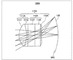
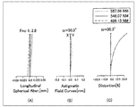
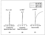
- FIG. 3 is an aberration diagram showing spherical aberration (chromatic aberration), astigmatism, and distortion in Example 1.
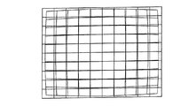
- FIG. 3 is a diagram showing a distortion grid in the first embodiment. It is a figure which shows the structural example of the imaging device which concerns on the 2nd embodiment. It is a figure which shows the surface number provided with respect to each lens which comprises each lens group of the imaging lens which concerns on the 2nd embodiment, a board
- Example 2 it is an aberrational figure which shows spherical aberration (chromatic aberration), astigmatism, and a distortion aberration.
- FIG. 6 is a diagram showing a distortion grid in the second embodiment. It is a figure which shows the structural example of the imaging device which concerns on the 3rd embodiment. It is a figure which shows the surface number provided with respect to each lens which comprises each lens group of the imaging lens which concerns on the 3rd embodiment, a board
- FIG. 10 is an aberration diagram showing spherical aberration (chromatic aberration), astigmatism, and distortion in Example 3.
- FIG. 6 is a diagram showing a distortion grid in the third embodiment.
- FIG. 10 is a diagram showing a distortion grid in the fourth embodiment. It is a figure which shows the structural example of the imaging device which concerns on the 5th embodiment.
- FIG. 10 is an aberration diagram showing spherical aberration (chromatic aberration), astigmatism, and distortion in Example 5.
- FIG. 10 is a diagram showing a distortion grid in the fifth embodiment. It is a figure which shows the structural example of the imaging device which concerns on the 6th embodiment. It is a figure which shows the surface number provided with respect to the lens and board
- FIG. 10 is an aberration diagram showing spherical aberration (chromatic aberration), astigmatism, and distortion in Example 6.
- FIG. 10 is a diagram showing a distortion grid in Example 6. It is a figure which shows the structural example of the imaging device which concerns on the 7th embodiment. It is a figure which shows the structural example of the imaging device which concerns on the 8th embodiment. It is a figure which shows the structural example of the imaging device which concerns on the 9th embodiment. It is a figure which shows the surface number provided with respect to the lens and board
- FIG. 10 is an aberration diagram showing spherical aberration (chromatic aberration), astigmatism, and distortion in Example 9. FIG. 10 is a diagram showing a distortion grid in Example 9. It is a figure which shows the structural example of the imaging device which concerns on the 10th embodiment.
- FIG. 10 is an aberration diagram showing spherical aberration (chromatic aberration), astigmatism, and distortion in Example 9.
- FIG. 10 is a diagram showing a distortion grid in Example 9. It is a figure which shows the structural example of the imaging device which concerns on the 10
- FIG. 32 is an aberration diagram showing spherical aberration (chromatic aberration), astigmatism, and distortion in the imaging device of FIG. 31. It is a figure which shows the distortion grating
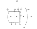
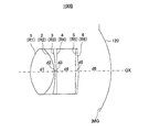
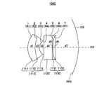
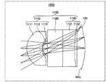
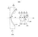
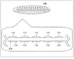
- FIG. 1 is a diagram illustrating a configuration example of the imaging apparatus according to the first embodiment.
- the imaging apparatus 100 includes a lens 110 and an imaging element 120 that are sequentially arranged from the object side OBJS toward the image plane side.
- This lens 110 is formed as a single focus lens.
- the imaging apparatus 100 basically includes an imaging element 120 that is curved with a concave toward the object side, and a group of lenses 110.
- the lens 110 is arranged in order from the object side to the image plane side without air being sandwiched, and the first lens 111 whose object side surface has a convex shape on the object side, and a transparent body provided with a diaphragm and an infrared cut filter As a glass substrate 112 and a second lens 113.
- the first lens 111 is preferably realized by applying an ultraviolet (UV) cured replica lens on the glass substrate 112. Further, it is possible to realize a high performance by applying a different replica glass material twice to form a doublet structure or three times to form a triplet structure. Configurations beyond the triplet configuration are also possible.
- UV ultraviolet
- the second lens 113 is preferably realized by applying a UV curing replica lens to the back side of the first lens 111 of the glass substrate 112.
- different replica glass materials may be applied twice to form a doublet structure, or may be applied three or more times to make a triplet structure or more.
- the first lens 111 has a strong positive power
- the second lens 113 has a weak positive or weak negative power.
- a strong positive (pincushion type) optical distortion is generated in the lens group due to the influence of the power configuration, and the negative (barrel type) optical distortion generated by bending the image pickup element is canceled, so that the entire image pickup element is obtained.
- preferable optical distortion is realized.
- the optical distortion of the lens group is 4% or more positive.
- the image plane IMG is provided with an imaging plane (image receiving plane) of a solid-state imaging device such as a CCD sensor or a CMOS sensor.
- a cover glass made of resin or glass, an infrared cut filter, a low-pass filter, and other optical members are placed between the final image side surface and the image surface, or in front of the first surface on the object side. May be.
- the left side is the object side (front)
- the right side is the image plane side (rear).
- the light beam incident from the object side is imaged on the image plane IMG of the image sensor 120.
- the imaging lens 110 of the present embodiment which is a single focus lens, is configured to satisfy the following conditional expressions (1) to (3).
- Conditional expression (1) defines conditions regarding the power of the first lens 111.
- fL1 indicates the focal length of the first lens 111
- f indicates the focal length of the lens system.
- Conditional expression (1) is necessary for the following reasons. If the upper limit is exceeded, positive (pincushion type) optical distortion will not occur, and optical distortion will occur as a system, and the angle of incidence on the object-side incident first surface will differ for each image height, resulting in chromatic aberration. This is necessary because the optical properties cannot be obtained. If the lower limit is exceeded, the surface of the object-side incident first surface becomes a strong curved surface, which makes it impossible to manufacture.
- Conditional expression (2) defines a condition regarding the power of the second lens 113.
- fL2 indicates the focal length of the first lens 112
- f indicates the focal length of the lens system.
- Conditional expression (2) is necessary for the following reason. Exceeding the upper limit of the expression relating to minus is necessary because the angle of light incident on the image sensor becomes large and desirable camera characteristics cannot be obtained. If the lower limit of the expression relating to plus is exceeded, positive (pincushion type) optical distortion does not occur, and this is necessary because the system produces optical distortion.
- Conditional expression (3) defines conditions regarding the bending of the image sensor 120.
- Ri represents the radius of curvature of the image plane IMG.
- Conditional expression (3) is necessary for the following reason. If the upper limit is exceeded, the lens cannot correct the curvature of field, and this is necessary because the MTF deteriorates as the image height increases. If the lower limit is exceeded, the curvature of field is overcorrected, the MTF deteriorates as the image height increases, and it is necessary because it is difficult to bend in manufacturing.
- the aspherical shape of the lens is as follows when the direction from the object side to the image plane side is positive, k is a conical coefficient, A, B, C, and D are aspherical coefficients, and r is a central radius of curvature. It is represented by y represents the height of the light beam from the optical axis, and c represents the reciprocal (1 / r) of the central curvature radius r.
- X is the distance from the tangent plane to the aspheric vertex
- A is the fourth-order aspheric coefficient
- B is the sixth-order aspheric coefficient
- C is the eighth-order aspheric coefficient
- D is the tenth-order aspheric coefficient. Each aspheric coefficient is shown.
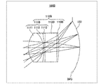
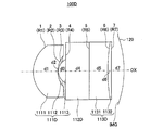
- FIG. 2 is a diagram showing surface numbers given to the lens and the substrate of the imaging apparatus according to the first embodiment.
- the first surface number is the object side surface (convex surface) of the first lens 111
- the second surface number is the boundary surface (bonding surface) between the image surface side surface of the first lens 111 and the object side surface of the glass substrate 112. Is granted.
- the third surface number is assigned to the boundary surface (bonding surface) between the image surface side surface of the glass substrate 112 and the object side surface of the second lens 113
- the fourth surface number is assigned to the image surface side surface of the second lens 113. Has been granted.
- the central curvature radius of the object side surface (first) 1 of the first lens 111 is set to R1.
- the central radius of curvature of the boundary surface (bonding surface) 2 between the image surface side surface of the first lens 111 and the object side surface of the glass substrate 112 is set to R2.
- the central radius of curvature of the boundary surface (bonding surface) 3 between the image surface side surface of the glass substrate 112 and the object side surface of the second lens 113 is set to R3.
- the central radius of curvature of the image plane side surface 4 of the second lens 113 is set to R4.
- the central curvature radii R2 and R3 of the surfaces 2 and 3 are infinite (INFINITY).
- the distance on the optical axis OX between the surface 1 and the surface 2 that is the thickness of the first lens 111 is d1
- the distance on OX is set to d2.
- the distance on the optical axis OX between the surface 3 and the surface 4 that is the thickness of the second lens 113 is set to d3
- the distance on the optical axis OX between the image surface side surface of the second lens 113 and the image surface IMG is set to d4.
- Example 1 according to specific numerical values of the lens 110 of the imaging apparatus 100 will be described below.
- surface numbers as shown in FIG. 2 are given to the lenses of the lens 110 and the glass substrate.
- Example 1 Table 1, Table 2, Table 3, and Table 4 show the numerical values of Example 1. Each numerical value of Example 1 corresponds to the lens 110 of FIG.
- the first embodiment is a design example for a 3 megapixel (Mage pixel) CMOS imager having a 1/6 size and a 1.1 ⁇ m pitch.
- the first embodiment includes the imaging element 120 and the group of lenses 110 that are curved with the concave facing the object side.
- the lens 110 is arranged in order from the object side to the image plane side without sandwiching air, the first lens 111 whose object side surface is convex toward the object side, and a glass substrate on which an aperture and an infrared cut filter are applied. 112 and the second lens 113.
- the first lens 111 is preferably realized by applying a UV curing replica lens on the glass substrate 112.
- the second lens is preferably realized by applying a UV effect replica lens to the back side of the first lens 111 of the glass substrate 112.
- the first lens 111 and the second lens 113 can be formed on a Schott D263T glass substrate by a replica process using NT33 glass material manufactured by Nitto Denko Corporation, for example.
- the power configuration is such that the first lens 111 has a strong positive power and a focal length of 4.1 mm, the second lens 113 has a weak positive and a focal length of 9.9 mm.
- Table 1 shows each lens corresponding to each surface number of the lens 110 in Example 1, the radius of curvature (R: mm), the interval (d: mm), the refractive index (nd), and the dispersion of the glass substrate (transparent body). The value ( ⁇ d) is shown.
- Table 2 shows fourth-order, sixth-order, eighth-order, and tenth-order aspherical coefficients of the surface 1 of the first lens 111 and the surface 4 of the second lens 113 including the aspherical surface in Example 1.
- K is the conic constant
- A is the fourth-order aspheric coefficient
- B is the sixth-order aspheric coefficient
- C is the eighth-order aspheric coefficient
- D is the tenth-order aspheric coefficient.
- Table 3 specifically shows the focal length f, the numerical aperture F, the half angle of view ⁇ , and the lens length H of the lens 110 in the first embodiment.
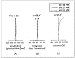
- the focal length f is set to 2.36 [mm]
- the numerical aperture F is set to 2.8
- the half angle of view ⁇ is set to 32.0 deg
- the lens length H is set to 3.23 [mm].
- Table 4 shows that, in Example 1, the above conditional expressions (1) to (3) are satisfied.
- the power (fL1 / f) of the first lens 111 is set to 1.72, which satisfies the condition defined by the conditional expression (1).
- the power (fL2 / f) of the second lens 113 is set to 4.21, which satisfies the positive condition defined by the conditional expression (2).
- the radius of curvature (Ri) of the image plane IMG of the image sensor 120 is set to ⁇ 1.31, which satisfies the condition defined by the conditional expression (3).
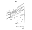
- FIG. 3 is an aberration diagram showing spherical aberration (chromatic aberration), astigmatism, and distortion in Example 1.
- 3A shows spherical aberration (chromatic aberration)
- FIG. 3B shows astigmatism
- FIG. 3C shows distortion.
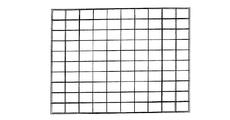
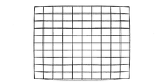
- FIG. 4 is a diagram illustrating a distortion grating in the first embodiment.
- an imaging apparatus including a lens having excellent imaging performance in which various aberrations of spherical surface, astigmatism, and distortion are well corrected.
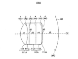
- FIG. 5 is a diagram illustrating a configuration example of the imaging apparatus according to the second embodiment.
- the imaging device 100A according to the second embodiment shown in FIG. 5 is different from the imaging device 100 according to the first embodiment shown in FIG. 1 in the following points.
- the first lens 111A is formed by the first lens element 1111 and the second lens element 1112
- the glass substrate 112A is formed by the first glass substrate 1121 and the second glass substrate 1122.
- the first lens 111A is formed on the first glass substrate 1121
- the second lens 113A is formed on the second glass substrate 1122.
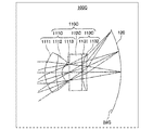
- FIG. 6 is a diagram showing surface numbers given to the lens and the substrate of the imaging apparatus according to the second embodiment.
- the first lens element 1111 has a first object side surface (convex surface)
- the second lens element 1112 has a second boundary surface (joint surface) between the image surface side surface of the first lens element 1111 and the object side surface of the second lens element 1112.
- No. face number is given.
- a third surface number is assigned to the boundary surface (bonding surface) between the image surface side surface of the second lens element 1112 and the object side surface of the first glass substrate 1121.
- a fourth surface number is assigned to the boundary surface (bonding surface) between the image surface side surface of the first glass substrate 1121 and the object side surface of the second glass substrate 1122.
- the fifth surface number is assigned to the boundary surface (bonding surface) between the image surface side surface of the second glass substrate 1122 and the object side surface of the second lens 113A, and the sixth surface is provided to the image surface side surface of the second lens 113A.
- a number is assigned.
- the center curvature radius of the object side surface (first) 1 of the first lens element 1111 is set to R1.
- the central radius of curvature of the boundary surface (joint surface) between the image surface side surface of the first lens element 111 and the object side surface of the second lens element 1112 is set to R2.
- the central radius of curvature of the boundary surface (bonding surface) between the image surface side surface of the second lens element 1112 and the object side surface of the first glass substrate 1121 is set to R3.
- the central radius of curvature of the boundary surface (bonding surface) between the image surface side surface of the first glass substrate 1121 and the object side surface of the second glass substrate 1122 is set to R4.
- the central radius of curvature of the boundary surface (bonding surface) between the image surface side surface of the second glass substrate 1122 and the object side surface of the second lens 113A is set to R5.
- the central radius of curvature of the image plane side surface of the second lens 113 is set to R6.
- the central radii of curvature R3, R4, and R5 of the surfaces 3, 4, and 5 are infinite (INFINITY).
- the distance on the optical axis OX between the surface 1 and the surface 2 that is the thickness of the first lens element 1111 is set to d1.
- the distance on the optical axis OX between the surface 2 and the surface 3 that is the thickness of the second lens element 1112 is set to d2.
- the distance on the optical axis OX between the surface 3 and the surface 4 that is the thickness of the first glass substrate 1121 is set to d3.
- the distance on the optical axis OX between the surface 4 and the surface 5 serving as the thickness of the second glass substrate 1122 is set to d4.
- the distance on the optical axis OX between the surface 5 and the surface 6 serving as the thickness of the second lens 113A is set to d5
- the distance on the optical axis OX between the image surface side surface of the second lens 113A and the image surface IMG is set to d6.
- Example 2 based on specific numerical values of the lens 110A of the imaging apparatus 100A will be described.
- surface numbers as shown in FIG. 6 are assigned to the lenses and the glass substrate of the lens 110A.
- Example 2 Table 5, Table 6, Table 7, and Table 8 show the numerical values of Example 2. Each numerical value of Example 2 corresponds to the lens 110A of FIG.
- the second embodiment is a design example for a 5 megapixel (Mage pixel) CMOS imager having a 1/5 size and a pitch of 1.1 ⁇ m. As described above, the second embodiment includes the imaging element 120A that is curved with a concave toward the object side and a group of lenses 110A.
- the lens 110A is arranged in order from the object side to the image surface side without air being sandwiched, and a first lens 111A having a convex object side surface on the object side, and a glass 112A provided with a diaphragm and an infrared cut filter And the second lens 113A.
- the first lens 111A is formed by a first lens element 1111 having a Abbe number of 57.3 and a biconvex lens and a second lens element 1112 having an Abbe number of 29.6 and a concave flat shape.
- the first lens 111A is preferably realized by applying a UV curing replica lens twice on the glass substrate 1121.
- the second lens 113A is preferably realized by applying a UV curing replica lens to the back side of the first lens 110A on the glass substrate.
- the first lens 110A and the second lens 113A may be formed on different substrates 1121 and 1122, and the planes of the substrates may be bonded to each other.
- the first lens 110A can be formed on a Schott D263T glass substrate by performing a replica process twice using, for example, Nitto Denko NT33 glass material and Asahi Kasei 414C glass material.
- the second lens 113A can be formed on the back side of the first lens 110A by a replica process using NT33 glass material manufactured by Nitto Denko Corporation.
- the power configuration is such that the first lens 110A has a strong positive power and a focal length of 4.9 mm, the second lens 113A has a weak positive and a focal length of 71.2 mm.
- 24.5% of positive (pincushion) optical distortion is generated in the lens due to the influence of the power configuration described above, and the TV distortion as a system is 0.4 (negative) as shown in FIG. %.
- Table 5 shows each lens corresponding to each surface number of the lens 110A in Example 2, the radius of curvature (R: mm), the interval (d: mm), the refractive index (nd), and the dispersion of the glass substrate (transparent body). The value ( ⁇ d) is shown.
- Table 16 shows fourth-order, sixth-order, eighth-order, and tenth-order aspherical coefficients of surface 1 and surface 2 of the first lens 111A including the aspheric surface in Example 2 and surface 6 of the second lens 113A.
- K is a conic constant
- A is a fourth-order aspheric coefficient
- B is a sixth-order aspheric coefficient
- C is an eighth-order aspheric coefficient
- D is a tenth-order aspheric coefficient. Represents.
- Table 7 specifically shows the focal length f, the numerical aperture F, the half angle of view ⁇ , and the lens length H of the lens 110A in the second embodiment.
- the focal length f is set to 3.12 [mm]
- the numerical aperture F is set to 2.8
- the half angle of view ⁇ is set to 30.3 deg
- the lens length H is set to 3.90 [mm].
- Table 8 shows that, in Example 2, the above conditional expressions (1) to (3) are satisfied.
- the power (fL1 / f) of the first lens 111A is set to 1.56, which satisfies the condition defined by the conditional expression (1).
- the power (fL2 / f) of the second lens 113A is set to 22.82, which satisfies the positive condition defined by the conditional expression (2).
- the curvature radius (Ri) of the image plane IMG of the image sensor 120A is set to ⁇ 1.53, which satisfies the condition defined by the conditional expression (3).
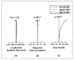
- FIG. 7 is an aberration diagram showing spherical aberration (chromatic aberration), astigmatism, and distortion in Example 2.
- 7A shows spherical aberration (chromatic aberration)
- FIG. 7B shows astigmatism
- FIG. 7C shows distortion.
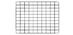
- FIG. 8 is a diagram showing a distortion grating in the second embodiment.
- an imaging apparatus including a lens having excellent imaging performance in which various aberrations of spherical surface, astigmatism, and distortion are satisfactorily corrected.
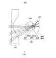
- FIG. 9 is a diagram illustrating a configuration example of the imaging apparatus according to the third embodiment.
- the imaging device 100B according to the third embodiment shown in FIG. 9 is different from the imaging device 100 according to the first embodiment shown in FIG. 1 in the following points.
- the first lens 111 ⁇ / b> B is formed by the first lens element 1111, the second lens element 1112, and the third lens element 1113.
- FIG. 10 is a diagram showing surface numbers given to the lens and the substrate of the imaging apparatus according to the third embodiment.
- the first lens element 1111 has a first object side surface (convex surface)
- the second lens element 1112 has a second boundary surface (joint surface) between the image surface side surface of the first lens element 1111 and the object side surface of the second lens element 1112.
- No. face number is given.
- a third surface number is assigned to the boundary surface (bonding surface) between the image surface side surface of the second lens element 1112 and the object side surface of the third lens element 1113.
- a fourth surface number is assigned to the boundary surface (bonding surface) between the image surface side surface of the third lens element 1113 and the object side surface of the glass substrate 112B.
- the fifth surface number is given to the boundary surface (bonding surface) between the image surface side surface of the glass substrate 112B and the object side surface of the second lens 113B, and the sixth surface number is assigned to the image surface side surface of the second lens 113B. Has been granted.
- the center curvature radius of the object side surface (first) 1 of the first lens element 1111 is set to R1.
- the central radius of curvature of the boundary surface (joint surface) between the image surface side surface of the first lens element 111 and the object side surface of the second lens element 1112 is set to R2.
- the central radius of curvature of the boundary surface (joint surface) between the image surface side surface of the second lens element 1112 and the object side surface of the third lens element 1113 is set to R3.
- the central radius of curvature of the boundary surface (bonding surface) between the image surface side surface of the third lens element 1113 and the object side surface of the glass substrate 112B is set to R4.
- Boundary surface (bonding surface) between the image surface side surface of the glass substrate 112B and the object side surface of the second lens 113B Is set to R5.
- the central radius of curvature of the image plane side surface of the second lens 113 is set to R6.
- the central radii of curvature R3, R4, and R5 of the surfaces 3, 4, and 5 are infinite (INFINITY).
- the distance on the optical axis OX between the surface 1 and the surface 2 that is the thickness of the first lens element 1111 is set to d1.
- the distance on the optical axis OX between the surface 2 and the surface 3 that is the thickness of the second lens element 1112 is set to d2.
- the distance on the optical axis OX between the surface 3 and the surface 4 that is the thickness of the third lens element 1113 is set to d3.
- the distance on the optical axis OX between the surface 4 and the surface 5 that is the thickness of the glass substrate 112B is set to d4.
- the distance on the optical axis OX between the surface 5 and the surface 6 serving as the thickness of the second lens 113B is set to d5
- the distance on the optical axis OX between the image surface side surface of the second lens 113B and the image surface IMG is set to d6.
- Example 3 according to specific numerical values of the lens 110B of the imaging apparatus 100B will be described below.
- surface numbers as shown in FIG. 10 are assigned to the lenses of the lens 110B and the glass substrate.
- Example 3 Table 9, Table 10, Table 11, and Table 12 show numerical values of Example 3. Each numerical value of Example 3 corresponds to the lens 110B of FIG. Embodiment 3 is a design example for a 5 megapixel (Mage pixel) CMOS imager having a 1/5 size and a 1.1 ⁇ m pitch.
- the third embodiment includes the imaging element 120B that is curved with a concave toward the object side and a group of lenses 110B.
- the lens 110B is arranged in order from the object side to the image plane side without sandwiching air, the first lens 111B having a convex object side surface on the object side, and a glass substrate on which an aperture and an infrared cut filter are applied. 112B and the second lens 113B.
- the first lens 110B has a first lens element 111 having an Abbe number of 57.3 and a positive power, a second lens element 1112 having an Abbe number of 29.6 and a negative power, and a first lens element having an Abbe number of 57.3 and a negative power.
- the three lens elements 1113 are formed.
- the first lens 110B is desirably realized by applying a UV curing replica lens three times on the glass substrate 112B.
- the second lens 113B is desirably realized by applying a UV curing replica lens to the back side of the first lens 110B of the glass substrate 112B.
- the first lens 110B can be formed on a Shot D263T glass substrate by performing an NT33 glass material manufactured by Nitto Denko Corporation, a 414C glass material manufactured by Asahi Kasei Co., Ltd., and NT33 manufactured by Nitto Denko Corporation in this order three times.
- the second lens 113B can be formed on the back side of the first lens 110B by a replica process using NT33 glass material manufactured by Nitto Denko Corporation.
- the power configuration is such that the first lens 110B has a strong positive power and a focal length of 5.0 mm, and the second lens 113B has a weak positive and a focal length of 7.0 mm.
- Table 9 shows each lens corresponding to each surface number of the lens 110B in Example 3, the radius of curvature (R: mm), the interval (d: mm), the refractive index (nd), and the dispersion of the glass substrate (transparent body). The value ( ⁇ d) is shown.
- Table 10 shows fourth-order, sixth-order, eighth-order, and tenth-order aspherical coefficients of the surface 1 of the first lens 111B including the aspheric surface and the surface 6 of the second lens 113B in Example 3.
- K is a conic constant
- A is a fourth-order aspheric coefficient
- B is a sixth-order aspheric coefficient
- C is an eighth-order aspheric coefficient
- D is a tenth-order aspheric coefficient. Represents.
- Table 11 specifically shows the focal length f, the numerical aperture F, the half angle of view ⁇ , and the lens length H of the lens 110B in Example 3.
- the focal length f is set to 2.62 [mm]
- the numerical aperture F is set to 2.8
- the half angle of view ⁇ is set to 38.2 deg
- the lens length H is set to 3.60 [mm].
- Table 12 shows that, in Example 3, the above conditional expressions (1) to (3) are satisfied.
- the power (fL1 / f) of the first lens 111B is set to 1.91, which satisfies the condition defined by the conditional expression (1).
- the power (fL2 / f) of the second lens 113B is set to 2.65, and the positive condition defined by the conditional expression (2) is satisfied.
- the radius of curvature (Ri) of the image plane IMG of the image sensor 120B is set to ⁇ 1.26, which satisfies the condition defined by the conditional expression (3).
- FIG. 11 is an aberration diagram showing spherical aberration (chromatic aberration), astigmatism, and distortion in Example 3.
- 11A shows spherical aberration (chromatic aberration)
- FIG. 11B shows astigmatism
- FIG. 11C shows distortion.
- FIG. 12 is a diagram illustrating a distortion grating in the third embodiment.
- an imaging apparatus including a lens having excellent imaging performance, in which various spherical, astigmatism, and distortion aberrations are corrected well.
- FIG. 13 is a diagram illustrating a configuration example of an imaging apparatus according to the fourth embodiment.
- the first lens 111 ⁇ / b> C is formed by the first lens element 1111, the second lens element 1112, and the third lens element 1113.
- the second lens 113 ⁇ / b> C is formed by the fourth lens element 1131 and the fifth lens element 1132.
- FIG. 14 is a diagram showing surface numbers given to the lens and the substrate of the imaging apparatus according to the fourth embodiment.
- the first lens element 1111 has a first object side surface (convex surface)
- the second lens element 1112 has a second boundary surface (joint surface) between the image surface side surface of the first lens element 1111 and the object side surface of the second lens element 1112.
- No. face number is given.
- a third surface number is assigned to the boundary surface (bonding surface) between the image surface side surface of the second lens element 1112 and the object side surface of the third lens element 1113.
- a fourth surface number is assigned to the boundary surface (bonding surface) between the image surface side surface of the third lens element 1113 and the object side surface of the glass substrate 112B.
- the fifth surface number is assigned to the boundary surface (bonding surface) between the image surface side surface of the glass substrate 112 ⁇ / b> C and the object side surface of the fourth lens element 1131.
- the sixth surface number is assigned to the boundary surface (bonding surface) between the image surface side surface of the second lens element 1131 and the object side surface of the fifth lens element 1132, and the seventh surface number is applied to the image surface side surface of the fifth lens element 1132. The surface number is given.
- the central curvature radius of the object side surface (first) 1 of the first lens element 1111 is set to R1.
- the central radius of curvature of the boundary surface (joint surface) between the image surface side surface of the first lens element 111 and the object side surface of the second lens element 1112 is set to R2.
- the central radius of curvature of the boundary surface (joint surface) between the image surface side surface of the second lens element 1112 and the object side surface of the third lens element 1113 is set to R3.
- the central radius of curvature of the boundary surface (bonding surface) between the image surface side surface of the third lens element 1113 and the object side surface of the glass substrate 112B is set to R4.
- the central radius of curvature of the boundary surface (joint surface) between the image surface side surface of the glass substrate 112C and the object side surface of the fourth lens element 1131 is set to R5.
- the central radius of curvature of the boundary surface (joint surface) between the image surface side surface of the second lens element 1131 and the object side surface of the fifth lens element 1132 is set to R6.
- the central radius of curvature of the image plane side surface of the fifth lens element 1132 is set to R7.
- the central radii of curvature R4 and R5 of the surfaces 4 and 5 are infinite (INFINITY).
- the distance on the optical axis OX between the surface 1 and the surface 2 which is the thickness of the first lens element 1111 is set to d1.
- the distance on the optical axis OX between the surface 2 and the surface 3 that is the thickness of the second lens element 1112 is set to d2.
- the distance on the optical axis OX between the surface 3 and the surface 4 that is the thickness of the third lens element 1113 is set to d3.
- the distance on the optical axis OX between the surface 4 and the surface 5 serving as the thickness of the glass substrate 112C is set to d4.
- the distance on the optical axis OX between the surface 5 and the surface 6 that is the thickness of the fourth lens element 1131 is set to d5.
- the distance on the optical axis OX between the surface 6 and the surface 7 that is the thickness of the fifth lens element 1132 is set to d6.
- the distance on the optical axis OX between the image surface side surface of the fifth lens element 1132 and the image surface IMG is set to d7.
- Example 4 based on specific numerical values of the lens 110C of the imaging device 100C will be described.
- surface numbers as shown in FIG. 14 are assigned to the lenses of the lens 110C and the glass substrate.
- Example 4 Table 13, Table 14, Table 15, and Table 16 show numerical values of Example 4. Each numerical value of Example 3 corresponds to the lens 110C of FIG.
- Example 4 is a design example for an 8-megapixel CMOS imager having a 1 ⁇ 4 size and a 1.1 ⁇ m pitch.
- the fourth embodiment includes the imaging element 120C that is curved with the concave facing the object side and a group of lenses 110C.
- the lens 110C is arranged in order from the object side to the image plane side without sandwiching air, the first lens 111C having a convex object side surface on the object side, and a glass substrate on which a diaphragm and an infrared cut filter are applied. 112C and the second lens 113C.
- the first lens 110C includes a first lens element 111 having an Abbe number of 57.3 and a positive power, a second lens element 1112 having an Abbe number of 29.6 and a negative power, and a first lens element having an Abbe number of 57.3 and a negative power.
- the three lens elements 1113 are formed.
- the second lens 113C is formed by a fourth lens element 1131 having an Abbe number of 57.3 and a negative power and a second lens element 1132 having an Abbe number of 29.6 and a positive power.
- the first lens 110C is desirably realized by applying a UV curing replica lens three times on the glass substrate 112C.
- the second lens 113C is preferably realized by applying a UV curing replica lens twice on the back side of the first lens 110C of the glass substrate 112C.
- the first lens 110C can be formed on a Shot D263T glass substrate by performing a replica process three times in order of Nitto Denko NT33 glass material, Asahi Kasei 414C glass material and Nitto Denko NT33.
- the 2nd lens 113C can form the NT33 glass material made from Nitto Denko, and Asahi Kasei 414C in order by the replica process in the back side of the 1st lens 110C.
- the power configuration is such that the first lens 110C has a strong positive power and a focal length of 5.6 mm, and the second lens 113C has a weak positive and a focal length of 40.5 mm.
- the lens due to the influence of the power configuration described above, the lens generates a positive (pincushion) optical distortion of 35.8%, and the system has a TV distortion of 0.6 (negative) as shown in FIG. %.
- Table 13 shows each lens corresponding to each surface number of the lens 110C in Example 4, the radius of curvature (R: mm), the interval (d: mm), the refractive index (nd), and the dispersion of the glass substrate (transparent body). The value ( ⁇ d) is shown.
- Table 14 shows the 4th, 6th, 8th, and 10th order aspherical surfaces of the surface 1, surface 2 and surface 3 of the first lens 111C including the aspherical surface in Example 4 and the surfaces 6 and 7 of the second lens 113C. Indicates the coefficient.
- K is a conic constant
- A is a fourth-order aspheric coefficient
- B is a sixth-order aspheric coefficient
- C is an eighth-order aspheric coefficient
- D is a tenth-order aspheric coefficient. Represents.
- Table 15 specifically shows the focal length f, the numerical aperture F, the half field angle ⁇ , and the lens length H of the lens 110C in the fourth embodiment.
- the focal length f is set to 3.48 [mm]
- the numerical aperture F is set to 2.8
- the half angle of view ⁇ is set to 33.7 deg
- the lens length H is set to 4.20 [mm].
- Table 16 shows that, in Example 4, the above conditional expressions (1) to (3) are satisfied.
- the power (fL1 / f) of the first lens 111C is set to 1.61, which satisfies the condition defined by the conditional expression (1).
- the power (fL2 / f) of the second lens 113C is set to 11.64, which satisfies the positive condition defined by the conditional expression (2).
- the radius of curvature (Ri) of the image plane IMG of the image sensor 120C is set to ⁇ 1.44, which satisfies the condition defined by the conditional expression (3).
- FIG. 15 is an aberration diagram showing spherical aberration (chromatic aberration), astigmatism, and distortion in Example 4.
- 15A shows spherical aberration (chromatic aberration)
- FIG. 15B shows astigmatism
- FIG. 15C shows distortion.
- FIG. 16 is a diagram illustrating a distortion grating in the fourth embodiment.
- an imaging device including a lens having excellent imaging performance, in which various spherical, astigmatism, and distortion aberrations are well corrected.
- FIG. 17 is a diagram illustrating a configuration example of an imaging apparatus according to the fifth embodiment.
- the first lens 111 ⁇ / b> D is formed by the first lens element 1111, the second lens element 1112, and the third lens element 1113.
- the second lens 113D is formed by the fourth lens element 1131 and the fifth lens element 1132.
- FIG. 18 is a diagram illustrating surface numbers given to the lens and the substrate of the imaging apparatus according to the fifth embodiment.
- the first lens element 1111 has a first object side surface (convex surface)
- the second lens element 1112 has a second boundary surface (joint surface) between the image surface side surface of the first lens element 1111 and the object side surface of the second lens element 1112.
- No. face number is given.
- a third surface number is assigned to the boundary surface (bonding surface) between the image surface side surface of the second lens element 1112 and the object side surface of the third lens element 1113.
- a fourth surface number is assigned to the boundary surface (bonding surface) between the image surface side surface of the third lens element 1113 and the object side surface of the glass substrate 112D.
- the fifth surface number is assigned to the boundary surface (bonding surface) between the image surface side surface of the glass substrate 112D and the object side surface of the fourth lens element 1131.
- the sixth surface number is assigned to the boundary surface (bonding surface) between the image surface side surface of the second lens element 1131 and the object side surface of the fifth lens element 1132, and the seventh surface number is applied to the image surface side surface of the fifth lens element 1132. The surface number is given.
- the center curvature radius of the object side surface (first) 1 of the first lens element 1111 is set to R1.
- the central radius of curvature of the boundary surface (joint surface) between the image surface side surface of the first lens element 111 and the object side surface of the second lens element 1112 is set to R2.
- the central radius of curvature of the boundary surface (joint surface) between the image surface side surface of the second lens element 1112 and the object side surface of the third lens element 1113 is set to R3.
- the central radius of curvature of the boundary surface (bonding surface) between the image surface side surface of the third lens element 1113 and the object side surface of the glass substrate 112D is set to R4.
- the central radius of curvature of the boundary surface (bonding surface) between the image surface side surface of the glass substrate 112D and the object side surface of the fourth lens element 1131 is set to R5.
- the central radius of curvature of the boundary surface (joint surface) between the image surface side surface of the second lens element 1131 and the object side surface of the fifth lens element 1132 is set to R6.
- the central radius of curvature of the image plane side surface of the fifth lens element 1132 is set to R7.
- the central radii of curvature R4 and R5 of the surfaces 4 and 5 are infinite (INFINITY).
- the distance on the optical axis OX between the surface 1 and the surface 2 that is the thickness of the first lens element 1111 is set to d1.
- the distance on the optical axis OX between the surface 2 and the surface 3 that is the thickness of the second lens element 1112 is set to d2.
- the distance on the optical axis OX between the surface 3 and the surface 4 that is the thickness of the third lens element 1113 is set to d3.
- the distance on the optical axis OX between the surface 4 and the surface 5 that is the thickness of the glass substrate 112D is set to d4.
- the distance on the optical axis OX between the surface 5 and the surface 6 that is the thickness of the fourth lens element 1131 is set to d5.
- the distance on the optical axis OX between the surface 6 and the surface 7 that is the thickness of the fifth lens element 1132 is set to d6.
- the distance on the optical axis OX between the image surface side surface of the fifth lens element 1132 and the image surface IMG is set to d7.
- Example 5 according to specific numerical values of the lens 110D of the imaging apparatus 100D will be described below.
- surface numbers as shown in FIG. 18 are assigned to the lenses of the lens 110D and the glass substrate.
- Example 5 Table 17, Table 18, Table 19, and Table 20 show numerical values of Example 5.
- Each numerical value in the fifth embodiment corresponds to the lens 110F in FIG.
- Example 5 is a design example for an 8-megapixel CMOS imager having a 1 ⁇ 4 size and a 1.1 ⁇ m pitch.
- the fifth embodiment includes the imaging element 120D that is curved with the concave facing the object side, and a group of lenses 110D.
- the lens 110D is arranged in order from the object side to the image plane side without air being sandwiched, and the first lens 111D having the object side surface convex toward the object side, and a glass substrate on which a diaphragm and an infrared cut filter are applied 112D and the second lens 113D.
- the first lens 110D has a first lens element 111 having an Abbe number of 57.3 and a positive power, a second lens element 1112 having an Abbe number of 29.6 and a negative power, and a first lens element having an Abbe number of 57.3 and a negative power.
- the three lens elements 1113 are formed.
- the second lens 113D is formed by a fourth lens element 1131 having an Abbe number of 57.3 and a negative power and a fifth lens element 1132 having an Abbe number of 29.6 and a positive power.
- the first lens 110D is preferably realized by applying a UV curing replica lens three times on the glass substrate 112D.
- the second lens 113D is preferably realized by applying a UV curing replica lens twice on the back side of the first lens 110D of the glass substrate 112D.
- the first lens 110D can be formed on a Shot D263T glass substrate by performing a replica process three times in order of Nitto Denko NT33 glass material, Asahi Kasei 414C glass material, and Nitto Denko NT33.
- the 2nd lens 113D can form the NT33 glass material made from Nitto Denko, and Asahi Kasei 414C in order by the replica process in the back side of the 1st lens 110D.
- the power configuration is such that the first lens 110D has a strong positive power and a focal length of 8.18 mm, the second lens 113D has a weak negative and a focal length of ⁇ 647.8 mm.
- a positive (pincushion type) optical distortion of 13.9% is generated in the lens, and the TV distortion of the system is 1.9 (negative type) as shown in FIG. %.
- Table 17 shows each lens corresponding to each surface number of the lens 110D in Example 5, the radius of curvature (R: mm), the interval (d: mm), the refractive index (nd), and the dispersion of the glass substrate (transparent body). The value ( ⁇ d) is shown.
- Table 18 shows fourth-order, sixth-order, eighth-order, and tenth-order aspherical coefficients of the surface 1 of the first lens 111D including the aspheric surface and the surface 7 of the second lens 113C in Example 5.
- K is the conic constant
- A is the fourth-order aspheric coefficient
- B is the sixth-order aspheric coefficient
- C is the eighth-order aspheric coefficient
- D is the tenth-order aspheric coefficient. Represents.
- Table 19 specifically shows the focal length f, the numerical aperture F, the half angle of view ⁇ , and the lens length H of the lens 110D in Example 5.
- the focal length f is set to 5.56 [mm]
- the numerical aperture F is set to 2.8
- the half angle of view ⁇ is set to 28.9 deg
- the lens length H is set to 7.64 [mm].
- Table 20 shows that, in Example 5, the above conditional expressions (1) to (3) are satisfied.
- the power (fL1 / f) of the first lens 111D is set to 1.47, which satisfies the condition defined by the conditional expression (1).
- the power (fL2 / f) of the second lens 113D is set to ⁇ 116.5, which satisfies the negative condition defined by the conditional expression (2).
- the radius of curvature (Ri) of the image plane IMG of the image sensor 120D is set to ⁇ 1.53, which satisfies the condition defined by the conditional expression (3).
- FIG. 19 is an aberration diagram showing spherical aberration (chromatic aberration), astigmatism, and distortion in Example 5.
- 19A shows spherical aberration (chromatic aberration)
- FIG. 19B shows astigmatism
- FIG. 19C shows distortion.
- FIG. 20 is a diagram illustrating a distortion grating in the fifth embodiment.
- an imaging apparatus including a lens having excellent imaging performance in which various aberrations of spherical surface, astigmatism, and distortion are well corrected.
- the imaging element is curved with a concave toward the object side, and is formed of a group of lenses, and the lens is directed from the object side to the image plane side.
- the case where the air is not sandwiched is described as an example.
- an example in which the imaging element is curved with a concave toward the object side and formed of lenses of two or more groups is taken as an example.
- FIG. 21 is a diagram illustrating a configuration example of an imaging apparatus according to the sixth embodiment.
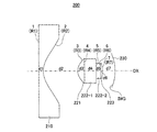
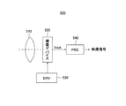
- An imaging apparatus 200 basically includes two lenses, a first lens group 210 and a second lens group 220, which are arranged in order from the object side OBJS toward the image plane side. It has an LNS and an image sensor 230 that is curved with its concave facing the object side.
- the imaging apparatus 200 includes the imaging element 230 that is curved with the concave facing the object side and the two groups of lenses LNS.
- the lens LNS includes a first lens group 210 and a second lens group 220 that are sequentially arranged from the object side toward the image plane side.
- the second lens group 220 includes a first lens 221 that is disposed in order without sandwiching air, the object side surface is convex toward the object side, a transparent body 222 (222-1, 222-2), and a second lens. 223.
- the transparent body 222 is preferably formed of a glass substrate, and is preferably subjected to a diaphragm or an infrared cut filter.
- the first lens group 210 is constituted by a negative power lens using an aspheric surface
- the second lens group 220 is constituted as follows.
- the first lens 221 of the second lens group 220 has a strong positive power and is preferably realized by applying a UV effect replica lens on a glass substrate. Further, it is possible to realize a high performance by applying a different replica glass material twice to form a doublet structure or three times to form a triplet structure. Configurations beyond the triplet configuration are also possible.
- the second lens 223 of the second lens group 220 has a weak positive or negative power, and is preferably realized by applying a UV effect replica lens on the back side of the first lens 221 of the glass substrate.
- different replica glass materials may be applied twice to form a doublet structure, or may be applied three or more times to make a triplet structure or more.
- the optical distortion of the lens group is 4% or more positive.
- the imaging surface IMG is provided with an imaging surface (image receiving surface) of a solid-state imaging device such as a CCD sensor or a CMOS sensor, as in the first embodiment.
- a cover glass made of resin or glass, an infrared cut filter, a low-pass filter, and other optical members are placed between the final image side surface and the image surface, or in front of the first surface on the object side. May be.
- the left side is the object side (front)
- the right side is the image plane side (rear).
- the light beam incident from the object side is imaged on the image plane IMG of the image sensor 230.
- the imaging lens of the present embodiment which is a single focus lens, is configured to satisfy the following conditional expressions (1) to (3).
- Conditional expression (1) defines conditions regarding the power of the first lens group 210.
- fG1 represents the focal length of the first lens group 210
- f represents the focal length of the lens system.
- Conditional expression (1) is necessary for the following reasons. If the upper limit is exceeded, the power becomes too strong and the actual assembly accuracy that can be achieved is not necessary. If the lower limit is exceeded, the negative power becomes too weak, and the advantage of bringing the negative power to the first lens group 210 cannot be obtained. That is, when the lower limit is exceeded, for example, the apparent exit pupil position is brought forward to reduce the chief ray incident angle to the image sensor, the back focus can be increased, the deterioration of the peripheral light amount, etc. are weak. This is necessary because sufficient optical characteristics cannot be obtained.
- Conditional expression (2) defines a condition relating to the power of the second lens group 220.
- fG1 represents the focal length of the second lens group 220
- f represents the focal length of the lens system.
- Conditional expression (2) is necessary for the following reason. Exceeding the upper limit is necessary because positive (pound) optical distortion does not occur and the system cannot be used. If the lower limit is exceeded, the power becomes too strong and the actual assembly accuracy that can be achieved is not necessary.
- Conditional expression (3) defines conditions regarding the bending of the image sensor 120.
- Ri represents the radius of curvature of the image plane IMG.
- Conditional expression (3) is necessary for the following reason. If the upper limit is exceeded, the lens cannot correct the curvature of field, and this is necessary because the MTF deteriorates as the image height increases. If the lower limit is exceeded, the curvature of field is overcorrected, the MTF deteriorates as the image height increases, and it is necessary because it is difficult to bend in manufacturing.
- conditional expressions (1) to (3) are common to the sixth to ninth embodiments, which will be described below, and are suitable for individual imaging elements or imaging apparatuses by adopting them as necessary. A more favorable imaging performance and a compact optical system are realized.
- the aspherical shape of the lens is positive in the direction from the object side to the image plane side
- k is a conical coefficient
- A, B, C, and D are aspherical coefficients
- r is a central radius of curvature. Is expressed by the above-mentioned [Equation 1].
- y represents the height of the light beam from the optical axis
- c represents the reciprocal (1 / r) of the central curvature radius r.
- A is the fourth-order aspheric coefficient
- B is the sixth-order aspheric coefficient
- C is the eighth-order aspheric coefficient
- D is the tenth-order aspheric coefficient.
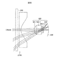
- FIG. 22 is a diagram showing surface numbers given to the lens and the substrate of the imaging apparatus according to the first embodiment.
- No. 1 is assigned to the object side surface of the first lens group 210
- No. 2 surface number is assigned to the image side surface of the first lens group 210
- No. 3 is given to the object side (convex surface) surface of the first lens 221 of the second lens group 220, and the boundary surface (bonding surface) between the image surface side surface of the first lens 221 and the object side surface of the transparent body 222-1.
- No. 5 is given to the boundary surface (bonding surface) between the image surface side surface of the transparent body 222-1 and the object side surface of the transparent body 222-2, and the image surface side surface of the transparent body 222-2 and the object of the second lens 223 are provided.
- No. 6 is given to the boundary surface (joint surface) with the side surface.
- No. 7 is given to the image surface side surface of the second lens 223.
- the center curvature radius of the object side surface (first) 1 of the first lens group 210 is set to R1.
- the central curvature radius of the image surface side surface 2 of the first lens group 210 is set to R2.
- the central curvature radius is set to R3 on the object side (convex surface) surface 3 of the first lens 221 of the second lens group 220, and the boundary surface between the image surface side surface of the first lens 221 and the object side surface of the transparent body 222-1 (
- the center curvature radius of the joint surface 4 is set to R4.
- the central curvature radius of the boundary surface (bonding surface) 5 between the image surface side surface of the transparent body 222-1 and the object side surface of the transparent body 222-2 is R5, and the image surface side surface of the transparent body 222-2 and the second lens 223 are
- the center curvature radius of the object side surface 6 is set to R6.
- the central radius of curvature of the image plane side surface 7 of the second lens 223 is set to R7.
- the central radii of curvature R4, R5, and R6 of the surfaces 4, 5, and 6 are infinite (INFINITY).
- the distance on the optical axis OX between the surface 1 and the surface 2 that is the thickness of the first lens group 210 is d1
- the image side surface 2 of the first lens group 210 and the second lens group 220 are the same.
- the distance on the optical axis OX between the object side surfaces 3 of the first lens 221 is set to d2.
- the distance on the optical axis OX between the surface 3 and the surface 4 that is the thickness of the first lens 221 is set to d3.
- the distance on the optical axis OX between the surface 4 and the surface 5 that is the thickness of the transparent body 222-1 is set to d4.
- the distance on the optical axis OX between the surface 5 and the surface 6 that is the thickness of the transparent body 222-2 is set to d5.
- the distance on the optical axis OX between the surface 6 and the surface 7 that is the thickness of the second lens 223 is set to d6, and the distance on the optical axis OX between the image surface side surface of the second lens 223 and the image surface IMG is d7. Is set.
- Example 6 based on specific numerical values of the lens of the imaging apparatus 200 will be described.
- surface numbers as shown in FIG. 22 are given to the lenses and the transparent body.
- Example 6 Table 21, Table 22, and Table 23 show numerical values of Example 6. Each numerical value of Example 6 corresponds to FIG.
- Example 6 is a design example of an in-vehicle camera, a PC camera, a surveillance camera, and the like for a 1.3M CMOS imager having a 1 ⁇ 4 size and a pitch of 2.8 ⁇ m.
- the imaging apparatus 200 is configured by an imaging element 230 that is curved with a concave toward the object side and two groups of lenses, and the lens is configured by an aspherical lens in which the first lens group 210 has negative power.
- the aspheric lens a material such as a glass mold, plastic, or a casting type lens is suitable.
- the second lens group 220 includes a first lens 221 that is arranged in order from the object side to the image plane side without air being sandwiched, the object side surface having a convex shape on the object side, an aperture and an infrared cut filter.
- the glass substrate (transparent body) 222 and the weak second lens 223 are configured.
- the first lens 221 is preferably realized by applying a UV effect replica lens on the opposite surface of the stop on the glass substrate on which the stop or IR cut filter is applied.
- the second lens 223 is preferably realized by applying a UV effect replica lens to the glass substrate.
- the second lens 223 may be applied to the back of the first lens 221, or may be applied to another glass substrate and the glass substrates may be bonded to each other.
- the first lens 221 and the second lens 223 can be formed on a Schott D263T glass substrate by a replica process using, for example, Nitto Denko NT33 glass material.
- the power configuration is such that the first lens group 210 has a strong negative power and a focal length of ⁇ 5.52 mm, the second lens group 220 has a weak positive and a focal length of 2.67 mm. Since the focal length of the optical system is 1.80 mm, conditional expression (1) is ⁇ 3.07 and conditional expression (2) is 1.48, which satisfies the requirements of the conditional expression.
- the lens generates a positive (pincushion) optical distortion of 25.8%, and the system has a TV distortion of 3.8 (negative) as shown in FIG. %.
- a compact imaging system with a short optical total length of 10 mm is realized, which is bright as Fno 2.8 and has a wide angle of half angle of view of 52.5 degrees, with various optical aberrations corrected as shown in FIG. .
- Table 21 shows each lens corresponding to each surface number of the lens in Example 6, the radius of curvature (R: mm), the interval (d: mm), the refractive index (nd), and the dispersion value of the glass substrate (transparent body). ( ⁇ d) is shown.
- Table 22 shows the fourth and sixth orders of the second surface of the first lens group 210 including the aspheric surface in Example 6, the third surface of the first lens 211 of the second lens group, and the seventh surface of the second lens 223. , 8th and 10th order aspherical coefficients.
- K is a conic constant
- A is a fourth-order aspheric coefficient
- B is a sixth-order aspheric coefficient
- C is an eighth-order aspheric coefficient
- D is a tenth-order aspheric coefficient. Represents.
- Table 23 specifically shows the focal length f, the numerical aperture F, the half angle of view ⁇ , and the lens length H of the lens in Example 6.
- the focal length f is set to 1.80 [mm]
- the numerical aperture F is set to 2.8
- the half angle of view ⁇ is set to 52.5 deg
- the lens length H is set to 10.0 [mm].
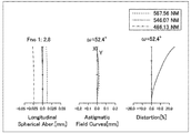
- FIG. 23 is an aberration diagram showing spherical aberration (chromatic aberration), astigmatism, and distortion in Example 6.
- 23A shows spherical aberration (chromatic aberration)
- FIG. 23B shows astigmatism
- FIG. 23C shows distortion.
- FIG. 24 is a diagram showing a distortion grating in the sixth embodiment.
- an imaging device including a lens having excellent imaging performance in which various aberrations of spherical surface, astigmatism, and distortion are well corrected.
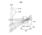
- FIG. 25 is a diagram illustrating a configuration example of an imaging apparatus according to the seventh embodiment.
- the image pickup apparatus 200A shown in FIG. 25 has a basic configuration similar to that of the image pickup apparatus 200 shown in FIG. 21.
- the first lens group 210A is made of plastic, and a cover glass 240 is disposed in front so that it can be used outdoors. It is.
- Example 7 corresponding to the seventh embodiment the basic optical parameters are almost the same as those in Example 6, and therefore description thereof is omitted here.
- FIG. 26 is a diagram illustrating a configuration example of an imaging apparatus according to the eighth embodiment.
- the image pickup apparatus 200B in FIG. 26 has the same basic configuration as the image pickup apparatus 200 in FIG. 21, and uses a first lens group 210B in which a flat glass substrate 211B is provided with a replica lens 212B. Thereby, since it has the heat-resistant characteristic which can endure reflow, and since the outermost side is glass, it can be used outdoors. Furthermore, in the imaging device 200B, both the first lens group 210B and the second lens group 220 can be manufactured with a wafer optic in which a large number of replica lenses are provided on a glass substrate, which is suitable for inexpensive mass production. In Example 8 corresponding to the eighth embodiment, the basic optical parameters are almost the same as those in Example 6, and therefore description thereof is omitted here.
- FIG. 27 is a diagram illustrating a configuration example of an imaging apparatus according to the ninth embodiment.
- the first lens group 210C is composed of an aspheric lens having negative power, and the aspheric lens is a normal replica lens 212C in which a replica lens is applied to the imaging surface side of the spherical glass 211C. It is realized with.
- FIG. 28 is a diagram showing surface numbers given to the lens and the substrate of the imaging apparatus according to the ninth embodiment.
- No. 1 is assigned to the object side surface of the spherical glass 211C of the first lens group 210, and the second is applied to the boundary surface (bonding surface) between the image surface side surface of the spherical glass 211 and the object side surface of the replica lens 212C.
- No. face number is given.
- a third surface number is assigned to the image surface side surface of the replica lens 212C.
- No. 4 is given to the object side (convex surface) surface of the first lens 221 of the second lens group 220, and the boundary surface (bonding surface) between the image surface side surface of the first lens 221 and the object side surface of the transparent body 222-1.
- No. 5 is assigned a surface number. No.
- a seventh surface number is assigned to the boundary surface (joint surface) with the side surface.
- the eighth lens is assigned to the image surface side surface of the second lens 223.
- the center curvature radius of the object side surface (first) 1 of the first lens group 210 is set to R1.
- the central radius of curvature of the boundary surface (bonding surface) between the image surface side surface 2 of the spherical glass 211C and the object side surface of the replica lens 212C is set to R2.
- the center radius of curvature of the image surface side surface 2 of the replica lens 212C of the first lens group 210 is set to R3.
- the central radius of curvature of the object side (convex surface) 4 of the first lens 221 of the second lens group 220 is set to R4, and the boundary surface between the image side surface of the first lens 221 and the object side surface of the transparent body 222-1 (
- the center curvature radius of the joint surface 5 is set to R5.
- the central curvature radius of the boundary surface (joint surface) 6 between the image surface side surface of the transparent body 222-1 and the object side surface of the transparent body 222-2 is R6, and the image surface side surface of the transparent body 222-2 and the second lens 223 are
- the center radius of curvature of the object side surface 7 is set to R7.
- the central radius of curvature of the image plane side surface 8 of the second lens 223 is set to R8.
- the central curvature radii R5, R6, and R7 of the surfaces 5, 6, and 7 are infinite (INFINITY).
- the distance on the optical axis OX between the surface 1 and the surface 2 that is the thickness of the spherical lens 211C of the first lens group 210 is d1, and the surface 2 and the surface that are the thickness of the replica lens 212C.
- the distance on the optical axis OX between the three is set to d2.
- the distance on the optical axis OX between the image side surface 3 of the replica lens 212C of the first lens group 210 and the object side surface 4 of the first lens 221 of the second lens group 220 is set to d3.
- the distance on the optical axis OX between the surface 4 and the surface 5 that is the thickness of the first lens 221 is set to d4.
- the distance on the optical axis OX between the surface 5 and the surface 6 that is the thickness of the transparent body 222-1 is set to d5.
- the distance on the optical axis OX between the surface 6 and the surface 7 which is the thickness of the transparent body 222-2 is set to d6.
- the distance on the optical axis OX between the surface 7 and the surface 8 that is the thickness of the second lens 223 is set to d7, and the distance on the optical axis OX between the image surface side surface of the second lens 223 and the image surface IMG is d8. Is set.
- Example 9 based on specific numerical values of the lens of the imaging apparatus 200C in FIG. 27 will be described.
- surface numbers as shown in FIG. 28 are assigned to the lenses and the transparent body.
- Example 9 Table 24, Table 25, and Table 26 show the numerical values of Example 9. Each numerical value of Example 9 corresponds to FIG.
- Example 9 is a design example of an in-vehicle camera, a PC camera, a surveillance camera, and the like for a 1.3M CMOS imager having a 1 ⁇ 4 size and a pitch of 2.8 ⁇ m.
- the ninth embodiment includes an imaging element 230 that is curved with a concave toward the object side and two groups of lenses.
- the first lens group 210C is composed of an aspherical lens 211 having negative power, and the aspherical lens is realized by a normal replica lens 212 having a replica lens 212C on the imaging surface side of the spherical glass 211C.
- the second lens 220 group includes a first lens 221 that is disposed in order from the object side to the image surface side without air being sandwiched, the object side surface having a convex shape on the object side, and an aperture and an infrared cut filter.
- the glass substrate (transparent body) 222 and the weak second lens 223 are configured.
- the first lens 221 is preferably realized by applying a UV effect replica lens on the opposite surface of the stop on the glass substrate on which the stop or IR cut filter is applied.
- the second lens 223 is preferably realized by applying a UV effect replica lens to the glass substrate 222.
- the second lens 223 may be applied to the back of the first lens 221 or may be applied to another glass substrate and the glass substrates may be bonded to each other.
- the first lens 221 and the second lens 223 can be formed on a Schott D263T glass substrate by a replica process using, for example, Nitto Denko NT33 glass material.
- the power configuration is such that the first lens group 210C has a strong negative power and a focal length of ⁇ 5.20 mm, the second lens group has a weak positive and a focal length of 2.64 mm. Since the focal length of the optical system is 1.735 mm, conditional expression (1) is ⁇ 3.00 and conditional expression (2) is 1.48, which satisfies the requirements of the conditional expression.
- Table 24 shows each lens corresponding to each surface number of the lens in Example 9, the radius of curvature (R: mm), the interval (d: mm), the refractive index (nd), and the dispersion value of the glass substrate (transparent body). ( ⁇ d) is shown. *
- Table 25 shows the fourth and sixth orders of the third surface of the first lens group 210 including the aspherical surface in Example 9, the fifth surface of the first lens 211 of the second lens group, and the eighth surface of the second lens 223. , 8th and 10th order aspherical coefficients.
- K is the conic constant
- A is the fourth-order aspheric coefficient
- B is the sixth-order aspheric coefficient
- C is the eighth-order aspheric coefficient
- D is the tenth-order aspheric coefficient. Represents.
- Table 26 specifically shows the focal length f, the numerical aperture F, the half angle of view ⁇ , and the lens length H of the lens in Example 9.
- the focal length f is set to 1.735 [mm]
- the numerical aperture F is set to 2.8
- the half angle of view ⁇ is set to 51.8 deg
- the lens length H is set to 10.0 [mm].
- FIG. 29 is an aberration diagram showing spherical aberration (chromatic aberration), astigmatism, and distortion in Example 9.
- 29A shows spherical aberration (chromatic aberration)
- FIG. 29B shows astigmatism
- FIG. 29C shows distortion.
- FIG. 30 is a diagram illustrating a distortion grating in the ninth embodiment. As can be seen from the figure, according to the ninth embodiment, an imaging apparatus including a lens with excellent spherical imaging, astigmatism, distortion, and excellent imaging performance can be obtained.
- FIG. 31 is a diagram illustrating a configuration example of the imaging apparatus according to the tenth embodiment.
- FIG. 32 is an aberration diagram showing spherical aberration (chromatic aberration), astigmatism, and distortion in the imaging apparatus of FIG. 32A shows spherical aberration (chromatic aberration), FIG. 32B shows astigmatism, and FIG. 32C shows distortion.
- FIG. 33 is a diagram showing a distortion grid in the imaging apparatus of FIG.
- the imaging apparatus 300 in FIG. 31 shows an example in which a sensor that is curved into a standard 4-group lens is used as a lens of a camera module for a mobile phone.
- This example is a design example for 13M having a size of 1 / 3.06 using a sensor with a pitch of 1.12 ⁇ m.
- the configuration data is Fno 2.8, focal length 3.66 mm, optical total length 4.0 mm, and horizontal angle of view 63.0 degrees.
- it has a positive (pincushion type) optical distortion as shown in FIG. 32, the TV distortion can be kept low by curving the imaging device as shown in FIG. In a normal design in which the imaging device 200 is flat, the same optical performance cannot be obtained unless the optical total length is about 4.4 mm.
- the entire aberration correction becomes advantageous by bending the imaging device, and optical
- the total length was shortened.
- the same effect as described above can be obtained by using a sensor (imaging device) curve and a lens that produces positive optical distortion.
- FIG. 34 is a diagram conceptually showing the wafer level optics according to the eleventh embodiment.
- FIG. 34 shows the concept. It is the conceptual diagram which gave many lenses simultaneously on the upper and lower sides of the glass substrate 410 which gave the infrared cut filter and the light-shielding stop by the replica process. In this way, by manufacturing a large number of lenses on the glass substrate 400 by a manufacturing method using a replica process and cutting them out individually, the first group lens and the second group lens of this embodiment can be manufactured. Alternatively, the lens wafer and the sensor wafer may be bonded in a wafer state and then cut out individually to form an imaging device.
- an image pickup apparatus configured by a group of lenses in which an image pickup element that can handle high pixels is curved is realized.
- the following effects can be obtained. 1) A diaphragm or an infrared cut filter can be provided on the substrate, and it can be formed as a medium diaphragm. Optical aberrations can be corrected efficiently, and an optical system that does not require the infrared cut filter to be provided as a separate part can be constructed. 2) Consists of a group attached to a glass substrate, the accuracy is determined by the lens manufacturing process, and there are no problems in assembling a plurality of lenses or reliability problems after manufacturing the lens.
- the negative optical distortion generated by bending the image sensor can be canceled by the positive optical distortion generated by the lens system, and the effect of simplifying the lens obtained by bending the image sensor can be maximized.
- a simple wide-angle lens having a structure with small optical distortion can be realized.
- a lens can be constituted by one group.
- the need for image surface correction with a lens can be reduced. Therefore, a wide-angle lens can be constituted by two groups, and since usually three or more groups are required, it is possible to reduce the size and cost.
- the object-side entrance surface of the lens is convex, and the difference in the lens incidence angle is small depending on the image height, so that chromatic aberration is difficult to occur. 7) With the above effects, it is possible to deal with various angles of view from narrow angles to wide angles. 8) An imaging device with a small projected area can be realized. 9) It can be made of a reflowable glass material, which is usually difficult with an inexpensive wide-angle lens, and an optimal system for a reflowable wide-angle camera or an in-vehicle camera can be constructed. 10) The lens can be made in the form of a wafer and can be mass-produced at low cost. 11) Since it is composed of a group of lenses, there is little variation in the focus direction of each lens.
- a lens module and a sensor wafer can be bonded together to make a camera module, and the camera module can be mass-produced at a low cost.
- a curved imaging device is used in a normal optical system, a short optical length that cannot be achieved normally can be achieved.
- the imaging devices 100, 100A to 100D, 200, 200A to 200C having the characteristics as described above are mounted on a digital camera using an imaging element such as a CCD or a CMOS sensor, particularly on a small electronic device such as a mobile phone. It can be applied as a camera lens.
- FIG. 35 is a block diagram illustrating a configuration example of an electronic apparatus in which the imaging apparatus according to the present embodiment is employed.
- the electronic apparatus 500 includes an optical system 510 to which the imaging lenses 100, 100A to 100D, 200, and 200A to 200C according to the present embodiment are applied, and a CCD or CMOS image sensor (solid-state imaging device). ) Is applicable.
- the optical system 510 guides incident light to an imaging surface including a pixel region of the imaging device 520 and forms a subject image.
- the electronic device 500 further includes a drive circuit (DRV) 530 that drives the imaging device 520 and a signal processing circuit (PRC) 540 that processes an output signal of the imaging device 520.
- DUV drive circuit
- PRC signal processing circuit
- the drive circuit 530 includes a timing generator (not shown) that generates various timing signals including a start pulse and a clock pulse that drive circuits in the imaging device 520, and drives the imaging device 520 with a predetermined timing signal. .
- the signal processing circuit 540 performs predetermined signal processing on the output signal of the imaging device 520.
- the signal processing circuit 540 can also perform distortion correction at the time of signal processing corresponding to the output signal of the imaging device 520, for example.
- the image signal processed by the signal processing circuit 540 is recorded on a recording medium such as a memory.
- the image information recorded on the recording medium is hard copied by a printer or the like.
- the image signal processed by the signal processing circuit 540 is displayed as a moving image on a monitor including a liquid crystal display.
- the above-described imaging apparatuses 100, 100A to 100D, 200, and 200A to 200C are mounted as the optical system 510 and the imaging device 520.
- An accurate camera can be realized.
- this technique can also take the following structures.
- the first lens is The imaging device according to any one of (1) to (4), wherein the imaging device has a doublet structure of a first lens element and a second lens element arranged in order from the object side.
- the first lens is The imaging apparatus according to any one of (1) to (4), wherein the imaging apparatus has a triplet structure including a first lens element, a second lens element, and a third lens element that are sequentially arranged from the object side.
- an Abbe number of the second lens element is smaller than that of the first lens element and the third lens element.
- the imaging device according to any one of (1) to (8), wherein the second lens has a doublet structure of at least a fourth lens element and a fifth lens element.
- the imaging device according to any one of (5) to (9), wherein at least one lens element is formed of an ultraviolet curable resin.
- the focal length fL1 of the first lens and the focal length fL2 of the second lens satisfy the following conditional expression, where f is the focal length of the lens system, and any one of (1) to (10) The imaging device described.
- the imaging device according to any one of (81) to (11), wherein the curvature radius Ri of the image plane of the imaging element satisfies the following conditional expression with a focal length of the lens system as f. ⁇ 5 ⁇ Ri / f ⁇ ⁇ 0.6 (13) a lens group having positive optical distortion; An imaging device that forms an image through the lens group, An imaging apparatus in which the imaging element is curved with a concave toward the object side, and negative optical distortion caused by the bending is canceled by the positive optical distortion of the lens group.
- the imaging device that forms an image through the lens, The lenses are arranged in order from the object side to the image plane side, A first lens group;
- An imaging apparatus comprising: a first lens having an object side surface convex toward the object side, a second lens group including a transparent body, and a second lens, which are arranged in order without sandwiching air.
- the second lens group is disposed in order from the object side to the image plane side without sandwiching air.
- a first replica lens A glass substrate;
- the focal length fG1 of the first lens group and the focal length fG2 of the second lens group satisfy the following conditional expression, where f is the focal length of the lens system, and any one of (13) to (18) The imaging device described in 1.
- the imaging device according to any one of (13) to (19), wherein the curvature radius Ri of the image plane of the imaging element satisfies the following conditional expression with a focal length of the lens system as f. ⁇ 40 ⁇ Ri / f ⁇ ⁇ 0.6
- the lens group is The imaging apparatus according to any one of (1) to (20), wherein the imaging apparatus has positive optical distortion and corrects negative optical distortion caused by imaging element bending.
- the imaging device according to any one of (1) to (21), wherein the optical distortion of the lens group is 4% or more positive.
- the imaging apparatus according to any one of (1) to (22), wherein distortion correction is performed during signal processing according to an output signal of the imaging element.
- an imaging device A signal processing circuit that performs signal processing on the output signal of the imaging device,
- the imaging apparatus is A group of lenses, An imaging device that forms an image through the lens, The lenses are arranged in order from the object side toward the image plane side without sandwiching air.
- the imaging device is an electronic device that is curved with a concave toward the object side.
- the imaging apparatus is A lens group having positive optical distortion; An imaging device that forms an image through the lens group, An electronic apparatus in which the imaging element is curved with a concave toward the object side, and negative optical distortion caused by the curvature is canceled by the positive optical distortion of the lens group.
- DRC drive circuit
Landscapes
- Physics & Mathematics (AREA)
- General Physics & Mathematics (AREA)
- Optics & Photonics (AREA)
- Engineering & Computer Science (AREA)
- Multimedia (AREA)
- Signal Processing (AREA)
- Health & Medical Sciences (AREA)
- Toxicology (AREA)
- Lenses (AREA)
- Studio Devices (AREA)
Priority Applications (1)
| Application Number | Priority Date | Filing Date | Title |
|---|---|---|---|
| US14/006,268 US10330888B2 (en) | 2011-04-26 | 2012-04-26 | Imaging device and electronic apparatus |
Applications Claiming Priority (4)
| Application Number | Priority Date | Filing Date | Title |
|---|---|---|---|
| JP2011-098113 | 2011-04-26 | ||
| JP2011098113 | 2011-04-26 | ||
| JP2011245392A JP6209308B2 (ja) | 2011-04-26 | 2011-11-09 | 撮像装置および電子機器 |
| JP2011-245392 | 2011-11-09 |
Publications (1)
| Publication Number | Publication Date |
|---|---|
| WO2012147841A1 true WO2012147841A1 (ja) | 2012-11-01 |
Family
ID=47072356
Family Applications (1)
| Application Number | Title | Priority Date | Filing Date |
|---|---|---|---|
| PCT/JP2012/061190 Ceased WO2012147841A1 (ja) | 2011-04-26 | 2012-04-26 | 撮像装置および電子機器 |
Country Status (3)
| Country | Link |
|---|---|
| US (1) | US10330888B2 (enExample) |
| JP (1) | JP6209308B2 (enExample) |
| WO (1) | WO2012147841A1 (enExample) |
Cited By (3)
| Publication number | Priority date | Publication date | Assignee | Title |
|---|---|---|---|---|
| US10591704B2 (en) | 2015-11-30 | 2020-03-17 | Sony Semiconductor Solutions Corporation | Imaging device and electronic device |
| US11353688B2 (en) | 2015-02-17 | 2022-06-07 | Largan Precision Co., Ltd. | Image capturing lens assembly, image capturing device and electronic device |
| US11513318B2 (en) | 2015-07-24 | 2022-11-29 | Largan Precision Co., Ltd. | Optical photographing lens assembly, image capturing device and electronic device |
Families Citing this family (21)
| Publication number | Priority date | Publication date | Assignee | Title |
|---|---|---|---|---|
| TWI467224B (zh) | 2012-11-21 | 2015-01-01 | Largan Precision Co Ltd | 光學拾像鏡片系統 |
| JP6032219B2 (ja) | 2014-01-24 | 2016-11-24 | トヨタ自動車株式会社 | 運転支援装置 |
| JP6376857B2 (ja) | 2014-06-20 | 2018-08-22 | キヤノン株式会社 | 撮像装置 |
| JP2016033542A (ja) * | 2014-07-31 | 2016-03-10 | ソニー株式会社 | 撮像レンズおよび撮像装置 |
| TWI510805B (zh) | 2014-08-12 | 2015-12-01 | Largan Precision Co Ltd | 攝影光學透鏡組、取像裝置以及電子裝置 |
| WO2016110883A1 (ja) | 2015-01-09 | 2016-07-14 | 株式会社ニコン | 撮像レンズおよび撮像装置 |
| JP6519355B2 (ja) | 2015-06-30 | 2019-05-29 | 株式会社デンソー | カメラ装置及び車載システム |
| US10578853B2 (en) | 2015-09-04 | 2020-03-03 | Olympus Corporation | Image forming optical system, image pickup apparatus, optical apparatus, and capsule endoscope |
| JP6572073B2 (ja) * | 2015-09-16 | 2019-09-04 | オリンパス株式会社 | 結像光学系及びそれを備えた光学装置 |
| JP2017085321A (ja) * | 2015-10-27 | 2017-05-18 | キヤノン株式会社 | 撮像装置およびその制御方法ならびにプログラム |
| JP6641933B2 (ja) * | 2015-11-30 | 2020-02-05 | コニカミノルタ株式会社 | 撮像レンズ及び撮像装置 |
| KR20160039588A (ko) | 2016-03-22 | 2016-04-11 | 주식회사 우리옵토 | 일정 곡률을 가지는 광학 렌즈상에 마이크로 패턴을 형성하는 방법 |
| US10802251B2 (en) | 2016-08-23 | 2020-10-13 | Largan Precision Co., Ltd. | Photographing optical lens assembly, image capturing apparatus and electronic device |
| TWI615627B (zh) | 2016-11-18 | 2018-02-21 | 大立光電股份有限公司 | 光學攝影鏡片系統、取像裝置及電子裝置 |
| JP6873741B2 (ja) * | 2017-02-24 | 2021-05-19 | オリンパス株式会社 | 撮像装置 |
| CN108111727A (zh) * | 2017-12-25 | 2018-06-01 | 信利光电股份有限公司 | 一种图像传感器以及摄像头模组 |
| CN110596862A (zh) * | 2019-09-03 | 2019-12-20 | 佛山科学技术学院 | 一种大视场紧凑型手机镜头 |
| CN110568587A (zh) * | 2019-09-03 | 2019-12-13 | 佛山科学技术学院 | 一种基于同心透镜的手机镜头 |
| DE102022124982B3 (de) * | 2022-09-28 | 2024-02-29 | Carl Zeiss Ag | Optische Anordnung für ein mobiles Gerät mit gekrümmter Detektor-Fläche |
| JP2024169230A (ja) * | 2023-05-25 | 2024-12-05 | 富士フイルム株式会社 | 撮像装置 |
| WO2025134541A1 (ja) * | 2023-12-22 | 2025-06-26 | ソニーグループ株式会社 | 光学系、および撮像装置 |
Citations (16)
| Publication number | Priority date | Publication date | Assignee | Title |
|---|---|---|---|---|
| JPS6396618A (ja) * | 1986-10-13 | 1988-04-27 | Canon Inc | 撮像装置 |
| JPS6396617A (ja) * | 1986-10-13 | 1988-04-27 | Canon Inc | 撮像装置 |
| JP2000347352A (ja) * | 1999-06-04 | 2000-12-15 | Fuji Photo Film Co Ltd | 撮影レンズ及びレンズ付きフイルムユニット |
| WO2001063915A1 (en) * | 2000-02-22 | 2001-08-30 | Hideaki Ishizuki | Light-receiving sensor enabling superwide-angle image pickup, and electronic digital camera comprising it |
| JP2004312239A (ja) * | 2003-04-04 | 2004-11-04 | Mitsubishi Electric Corp | 撮像装置 |
| WO2009104669A1 (ja) * | 2008-02-20 | 2009-08-27 | コニカミノルタオプト株式会社 | 撮像レンズ、撮像装置、携帯端末、および撮像レンズの製造方法 |
| JP2009223251A (ja) * | 2008-03-19 | 2009-10-01 | Olympus Corp | 撮像装置 |
| JP2009301046A (ja) * | 2007-02-19 | 2009-12-24 | Konica Minolta Opto Inc | 撮像レンズ、撮像装置、携帯端末、および撮像レンズの製造方法 |
| JP2010066445A (ja) * | 2008-09-10 | 2010-03-25 | Nikon Corp | 顕微鏡対物レンズ |
| WO2010087084A1 (ja) * | 2009-01-29 | 2010-08-05 | コニカミノルタオプト株式会社 | 撮像レンズ、撮像装置及び携帯端末 |
| JP2010266815A (ja) * | 2009-05-18 | 2010-11-25 | Konica Minolta Opto Inc | 撮像レンズ,撮像装置及び携帯端末 |
| WO2010143458A1 (ja) * | 2009-06-10 | 2010-12-16 | コニカミノルタオプト株式会社 | 撮像レンズ及び撮像装置 |
| JP2011017764A (ja) * | 2009-07-07 | 2011-01-27 | Konica Minolta Opto Inc | 撮像レンズ,撮像装置及び携帯端末 |
| JP2011039560A (ja) * | 2010-11-08 | 2011-02-24 | Canon Inc | ズームレンズ及びそれを有する撮像装置 |
| WO2011043023A1 (ja) * | 2009-10-06 | 2011-04-14 | ソニー株式会社 | 光学ユニットおよび撮像装置 |
| JP2011203313A (ja) * | 2010-03-24 | 2011-10-13 | Sony Corp | 光学ユニットおよび撮像装置 |
Family Cites Families (15)
| Publication number | Priority date | Publication date | Assignee | Title |
|---|---|---|---|---|
| US5004328A (en) | 1986-09-26 | 1991-04-02 | Canon Kabushiki Kaisha | Spherical lens and imaging device using the same |
| US5689376A (en) * | 1995-04-24 | 1997-11-18 | Eastman Kodak Company | Two element optical system, a camera using it and method of making the camera |
| JP3424030B2 (ja) * | 2001-01-31 | 2003-07-07 | カシオ計算機株式会社 | 撮影レンズ |
| JP2002300480A (ja) * | 2001-03-29 | 2002-10-11 | Fuji Photo Optical Co Ltd | 電子カメラ |
| WO2008102648A1 (ja) | 2007-02-19 | 2008-08-28 | Konica Minolta Opto, Inc. | 撮像レンズ及び撮像装置並びに携帯端末 |
| JP5212354B2 (ja) | 2007-02-19 | 2013-06-19 | コニカミノルタアドバンストレイヤー株式会社 | 撮像レンズ、撮像装置、携帯端末、および撮像レンズの製造方法 |
| JP3946245B1 (ja) * | 2007-03-08 | 2007-07-18 | マイルストーン株式会社 | 撮像レンズ |
| US20110010289A1 (en) * | 2007-05-03 | 2011-01-13 | Mastercard International Incorporated | Method And System For Controlling Risk Using Static Payment Data And An Intelligent Payment Device |
| CN101688967B (zh) * | 2007-07-04 | 2012-09-19 | 柯尼卡美能达精密光学株式会社 | 摄像透镜及摄像装置、便携终端 |
| KR100916502B1 (ko) * | 2007-08-10 | 2009-09-08 | 삼성전기주식회사 | 초소형 촬상 광학계 |
| DE102007045525A1 (de) * | 2007-09-24 | 2009-04-02 | Fraunhofer-Gesellschaft zur Förderung der angewandten Forschung e.V. | Bildsensor |
| CN101939682A (zh) * | 2008-02-12 | 2011-01-05 | 柯尼卡美能达精密光学株式会社 | 摄像透镜、摄像装置及便携终端 |
| WO2009125778A1 (ja) | 2008-04-11 | 2009-10-15 | 株式会社ニコン | 顕微鏡対物レンズ |
| JP5434450B2 (ja) | 2009-10-06 | 2014-03-05 | ソニー株式会社 | 光学ユニットおよび撮像装置 |
| JP5434457B2 (ja) | 2009-10-09 | 2014-03-05 | ソニー株式会社 | 光学ユニットおよび撮像装置 |
-
2011
- 2011-11-09 JP JP2011245392A patent/JP6209308B2/ja not_active Expired - Fee Related
-
2012
- 2012-04-26 WO PCT/JP2012/061190 patent/WO2012147841A1/ja not_active Ceased
- 2012-04-26 US US14/006,268 patent/US10330888B2/en not_active Expired - Fee Related
Patent Citations (16)
| Publication number | Priority date | Publication date | Assignee | Title |
|---|---|---|---|---|
| JPS6396618A (ja) * | 1986-10-13 | 1988-04-27 | Canon Inc | 撮像装置 |
| JPS6396617A (ja) * | 1986-10-13 | 1988-04-27 | Canon Inc | 撮像装置 |
| JP2000347352A (ja) * | 1999-06-04 | 2000-12-15 | Fuji Photo Film Co Ltd | 撮影レンズ及びレンズ付きフイルムユニット |
| WO2001063915A1 (en) * | 2000-02-22 | 2001-08-30 | Hideaki Ishizuki | Light-receiving sensor enabling superwide-angle image pickup, and electronic digital camera comprising it |
| JP2004312239A (ja) * | 2003-04-04 | 2004-11-04 | Mitsubishi Electric Corp | 撮像装置 |
| JP2009301046A (ja) * | 2007-02-19 | 2009-12-24 | Konica Minolta Opto Inc | 撮像レンズ、撮像装置、携帯端末、および撮像レンズの製造方法 |
| WO2009104669A1 (ja) * | 2008-02-20 | 2009-08-27 | コニカミノルタオプト株式会社 | 撮像レンズ、撮像装置、携帯端末、および撮像レンズの製造方法 |
| JP2009223251A (ja) * | 2008-03-19 | 2009-10-01 | Olympus Corp | 撮像装置 |
| JP2010066445A (ja) * | 2008-09-10 | 2010-03-25 | Nikon Corp | 顕微鏡対物レンズ |
| WO2010087084A1 (ja) * | 2009-01-29 | 2010-08-05 | コニカミノルタオプト株式会社 | 撮像レンズ、撮像装置及び携帯端末 |
| JP2010266815A (ja) * | 2009-05-18 | 2010-11-25 | Konica Minolta Opto Inc | 撮像レンズ,撮像装置及び携帯端末 |
| WO2010143458A1 (ja) * | 2009-06-10 | 2010-12-16 | コニカミノルタオプト株式会社 | 撮像レンズ及び撮像装置 |
| JP2011017764A (ja) * | 2009-07-07 | 2011-01-27 | Konica Minolta Opto Inc | 撮像レンズ,撮像装置及び携帯端末 |
| WO2011043023A1 (ja) * | 2009-10-06 | 2011-04-14 | ソニー株式会社 | 光学ユニットおよび撮像装置 |
| JP2011203313A (ja) * | 2010-03-24 | 2011-10-13 | Sony Corp | 光学ユニットおよび撮像装置 |
| JP2011039560A (ja) * | 2010-11-08 | 2011-02-24 | Canon Inc | ズームレンズ及びそれを有する撮像装置 |
Cited By (7)
| Publication number | Priority date | Publication date | Assignee | Title |
|---|---|---|---|---|
| US11353688B2 (en) | 2015-02-17 | 2022-06-07 | Largan Precision Co., Ltd. | Image capturing lens assembly, image capturing device and electronic device |
| US11921262B2 (en) | 2015-02-17 | 2024-03-05 | Largan Precision Co., Ltd. | Image capturing lens assembly, image capturing device and electronic device |
| US12189095B2 (en) | 2015-02-17 | 2025-01-07 | Largan Precision Co., Ltd. | Image capturing lens assembly, image capturing device and electronic device |
| US11513318B2 (en) | 2015-07-24 | 2022-11-29 | Largan Precision Co., Ltd. | Optical photographing lens assembly, image capturing device and electronic device |
| US11940667B2 (en) | 2015-07-24 | 2024-03-26 | Largan Precision Co., Ltd. | Optical photographing lens assembly, image capturing device and electronic device |
| US12321038B2 (en) | 2015-07-24 | 2025-06-03 | Largan Precision Co., Ltd. | Optical photographing lens assembly, image capturing device and electronic device |
| US10591704B2 (en) | 2015-11-30 | 2020-03-17 | Sony Semiconductor Solutions Corporation | Imaging device and electronic device |
Also Published As
| Publication number | Publication date |
|---|---|
| US10330888B2 (en) | 2019-06-25 |
| JP2012237966A (ja) | 2012-12-06 |
| JP6209308B2 (ja) | 2017-10-04 |
| US20140015997A1 (en) | 2014-01-16 |
Similar Documents
| Publication | Publication Date | Title |
|---|---|---|
| JP6209308B2 (ja) | 撮像装置および電子機器 | |
| US20240168262A1 (en) | Imaging lens system, image capturing unit and electronic device | |
| US20230161139A1 (en) | Imaging optical lens assembly, image capturing unit and electronic device | |
| US12158566B2 (en) | Optical image lens assembly, image capturing unit and electronic device including nine lenses of +−−+−−−+−, +−+++−−+−, +−−−++−+−, +−−+++−+− or +−−+−+−+− refractive powers | |
| JP5560699B2 (ja) | 光学ユニットおよび撮像装置 | |
| JP5636713B2 (ja) | 光学ユニットおよび撮像装置 | |
| US9557536B2 (en) | Zoom lens and image pickup device | |
| US7474478B2 (en) | Image pickup lens, image pickup apparatus and mobile terminal | |
| JP5699636B2 (ja) | 光学ユニットおよび撮像装置 | |
| US7031079B2 (en) | Taking lens system | |
| US11262543B2 (en) | Imaging lens including six lenses of +−++0− refractive powers | |
| JP2011133600A (ja) | 光学ユニットおよび撮像装置 | |
| WO2011043023A1 (ja) | 光学ユニットおよび撮像装置 | |
| US20220035131A1 (en) | Image lens assembly, image capturing unit and electronic device | |
| KR101925647B1 (ko) | 광학 유닛 및 촬상 장치 | |
| US11668907B2 (en) | Photographing optical lens assembly and electronic device | |
| US20200225448A1 (en) | Imaging lens | |
| JP5434450B2 (ja) | 光学ユニットおよび撮像装置 | |
| JP5589509B2 (ja) | 光学ユニットおよび撮像装置 | |
| JP6288168B2 (ja) | 撮像装置および電子機器 |
Legal Events
| Date | Code | Title | Description |
|---|---|---|---|
| 121 | Ep: the epo has been informed by wipo that ep was designated in this application |
Ref document number: 12777378 Country of ref document: EP Kind code of ref document: A1 |
|
| WWE | Wipo information: entry into national phase |
Ref document number: 14006268 Country of ref document: US |
|
| NENP | Non-entry into the national phase |
Ref country code: DE |
|
| 122 | Ep: pct application non-entry in european phase |
Ref document number: 12777378 Country of ref document: EP Kind code of ref document: A1 |