WO2012147784A1 - アナログ乗算回路、可変ゲインアンプ、検波回路及び物理量センサ - Google Patents
アナログ乗算回路、可変ゲインアンプ、検波回路及び物理量センサ Download PDFInfo
- Publication number
- WO2012147784A1 WO2012147784A1 PCT/JP2012/061075 JP2012061075W WO2012147784A1 WO 2012147784 A1 WO2012147784 A1 WO 2012147784A1 JP 2012061075 W JP2012061075 W JP 2012061075W WO 2012147784 A1 WO2012147784 A1 WO 2012147784A1
- Authority
- WO
- WIPO (PCT)
- Prior art keywords
- circuit
- current
- signal
- transistor
- input
- Prior art date
- Legal status (The legal status is an assumption and is not a legal conclusion. Google has not performed a legal analysis and makes no representation as to the accuracy of the status listed.)
- Ceased
Links
Images



Classifications
-
- G—PHYSICS
- G06—COMPUTING OR CALCULATING; COUNTING
- G06G—ANALOGUE COMPUTERS
- G06G7/00—Devices in which the computing operation is performed by varying electric or magnetic quantities
-
- G—PHYSICS
- G01—MEASURING; TESTING
- G01C—MEASURING DISTANCES, LEVELS OR BEARINGS; SURVEYING; NAVIGATION; GYROSCOPIC INSTRUMENTS; PHOTOGRAMMETRY OR VIDEOGRAMMETRY
- G01C19/00—Gyroscopes; Turn-sensitive devices using vibrating masses; Turn-sensitive devices without moving masses; Measuring angular rate using gyroscopic effects
- G01C19/56—Turn-sensitive devices using vibrating masses, e.g. vibratory angular rate sensors based on Coriolis forces
- G01C19/5776—Signal processing not specific to any of the devices covered by groups G01C19/5607 - G01C19/5719
-
- H—ELECTRICITY
- H03—ELECTRONIC CIRCUITRY
- H03D—DEMODULATION OR TRANSFERENCE OF MODULATION FROM ONE CARRIER TO ANOTHER
- H03D7/00—Transference of modulation from one carrier to another, e.g. frequency-changing
- H03D7/14—Balanced arrangements
- H03D7/1425—Balanced arrangements with transistors
- H03D7/1433—Balanced arrangements with transistors using bipolar transistors
-
- H—ELECTRICITY
- H03—ELECTRONIC CIRCUITRY
- H03D—DEMODULATION OR TRANSFERENCE OF MODULATION FROM ONE CARRIER TO ANOTHER
- H03D7/00—Transference of modulation from one carrier to another, e.g. frequency-changing
- H03D7/14—Balanced arrangements
- H03D7/1425—Balanced arrangements with transistors
- H03D7/145—Balanced arrangements with transistors using a combination of bipolar transistors and field-effect transistors
-
- H—ELECTRICITY
- H03—ELECTRONIC CIRCUITRY
- H03D—DEMODULATION OR TRANSFERENCE OF MODULATION FROM ONE CARRIER TO ANOTHER
- H03D7/00—Transference of modulation from one carrier to another, e.g. frequency-changing
- H03D7/14—Balanced arrangements
- H03D7/1425—Balanced arrangements with transistors
- H03D7/1458—Double balanced arrangements, i.e. where both input signals are differential
-
- H—ELECTRICITY
- H03—ELECTRONIC CIRCUITRY
- H03D—DEMODULATION OR TRANSFERENCE OF MODULATION FROM ONE CARRIER TO ANOTHER
- H03D7/00—Transference of modulation from one carrier to another, e.g. frequency-changing
- H03D7/14—Balanced arrangements
- H03D7/1425—Balanced arrangements with transistors
- H03D7/1491—Arrangements to linearise a transconductance stage of a mixer arrangement
-
- H—ELECTRICITY
- H03—ELECTRONIC CIRCUITRY
- H03F—AMPLIFIERS
- H03F3/00—Amplifiers with only discharge tubes or only semiconductor devices as amplifying elements
- H03F3/189—High-frequency amplifiers, e.g. radio frequency amplifiers
- H03F3/19—High-frequency amplifiers, e.g. radio frequency amplifiers with semiconductor devices only
- H03F3/193—High-frequency amplifiers, e.g. radio frequency amplifiers with semiconductor devices only with field-effect devices
-
- H—ELECTRICITY
- H03—ELECTRONIC CIRCUITRY
- H03F—AMPLIFIERS
- H03F3/00—Amplifiers with only discharge tubes or only semiconductor devices as amplifying elements
- H03F3/30—Single-ended push-pull [SEPP] amplifiers; Phase-splitters therefor
- H03F3/3001—Single-ended push-pull [SEPP] amplifiers; Phase-splitters therefor with field-effect transistors
- H03F3/3022—CMOS common source output SEPP amplifiers
-
- H—ELECTRICITY
- H03—ELECTRONIC CIRCUITRY
- H03F—AMPLIFIERS
- H03F3/00—Amplifiers with only discharge tubes or only semiconductor devices as amplifying elements
- H03F3/45—Differential amplifiers
- H03F3/45071—Differential amplifiers with semiconductor devices only
- H03F3/45076—Differential amplifiers with semiconductor devices only characterised by the way of implementation of the active amplifying circuit in the differential amplifier
- H03F3/45179—Differential amplifiers with semiconductor devices only characterised by the way of implementation of the active amplifying circuit in the differential amplifier using MOSFET transistors as the active amplifying circuit
- H03F3/45183—Long tailed pairs
-
- H—ELECTRICITY
- H03—ELECTRONIC CIRCUITRY
- H03F—AMPLIFIERS
- H03F3/00—Amplifiers with only discharge tubes or only semiconductor devices as amplifying elements
- H03F3/45—Differential amplifiers
- H03F3/45071—Differential amplifiers with semiconductor devices only
- H03F3/45479—Differential amplifiers with semiconductor devices only characterised by the way of common mode signal rejection
- H03F3/45632—Differential amplifiers with semiconductor devices only characterised by the way of common mode signal rejection in differential amplifiers with FET transistors as the active amplifying circuit
-
- H—ELECTRICITY
- H03—ELECTRONIC CIRCUITRY
- H03G—CONTROL OF AMPLIFICATION
- H03G1/00—Details of arrangements for controlling amplification
- H03G1/0005—Circuits characterised by the type of controlling devices operated by a controlling current or voltage signal
- H03G1/0017—Circuits characterised by the type of controlling devices operated by a controlling current or voltage signal the device being at least one of the amplifying solid-state elements
- H03G1/0023—Circuits characterised by the type of controlling devices operated by a controlling current or voltage signal the device being at least one of the amplifying solid-state elements in emitter-coupled or cascode amplifiers
-
- H—ELECTRICITY
- H03—ELECTRONIC CIRCUITRY
- H03D—DEMODULATION OR TRANSFERENCE OF MODULATION FROM ONE CARRIER TO ANOTHER
- H03D2200/00—Indexing scheme relating to details of demodulation or transference of modulation from one carrier to another covered by H03D
- H03D2200/0001—Circuit elements of demodulators
- H03D2200/0025—Gain control circuits
-
- H—ELECTRICITY
- H03—ELECTRONIC CIRCUITRY
- H03D—DEMODULATION OR TRANSFERENCE OF MODULATION FROM ONE CARRIER TO ANOTHER
- H03D2200/00—Indexing scheme relating to details of demodulation or transference of modulation from one carrier to another covered by H03D
- H03D2200/0001—Circuit elements of demodulators
- H03D2200/0033—Current mirrors
-
- H—ELECTRICITY
- H03—ELECTRONIC CIRCUITRY
- H03F—AMPLIFIERS
- H03F2203/00—Indexing scheme relating to amplifiers with only discharge tubes or only semiconductor devices as amplifying elements covered by H03F3/00
- H03F2203/45—Indexing scheme relating to differential amplifiers
- H03F2203/45244—Indexing scheme relating to differential amplifiers the differential amplifier contains one or more explicit bias circuits, e.g. to bias the tail current sources, to bias the load transistors
Definitions
- the present invention relates to an analog multiplication circuit using a multiplication core such as a Gilbert multiplication core, a detection circuit and a variable gain amplifier to which the analog multiplication circuit is applied, and a physical quantity sensor such as a vibration type angular velocity sensor using the detection circuit.
- a multiplication core such as a Gilbert multiplication core
- a detection circuit and a variable gain amplifier to which the analog multiplication circuit is applied
- a physical quantity sensor such as a vibration type angular velocity sensor using the detection circuit.
- a detection circuit In a physical quantity sensor represented by a vibration type angular velocity sensor, a detection circuit is generally required to detect an output signal of the sensor element and take out a signal component.
- a detection circuit a detection circuit using a Gilbert multiplier which is an analog multiplication circuit is known (for example, Patent Document 1).
- the Gilbert multiplier (Gilbert multiplier core) generally comprises a bi-differential circuit formed by four bipolar transistors and outputs a signal proportional to the product of two input signals.
- Gilbert multipliers using bipolar transistors have the problem of non-linearity resulting from the exponential characteristics of the bipolar transistors. Therefore, there is also known an analog multiplication circuit provided with a circuit for performing preprocessing for suppressing and linearizing non-linear components in the Gilbert multiplication core (for example, Non-Patent Document 1).
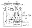
- the analog multiplication circuit 100 is configured of a Gilbert multiplication core 101 and a linearization circuit 102.
- the Gilbert multiplication core 101 comprises a bi-differential circuit formed by four bipolar transistors consisting of a pair of bipolar transistors Q1 and Q2 and a pair of bipolar transistors Q3 and Q4.
- the Gilbert multiplication core 101 is composed of a first input signal input to a first input terminal pair consisting of Ta and Tb which is an emitter common connection point of the transistor pair, and Tc and Td which is a base common connection point respectively.
- An output signal of a differential current proportional to the product of the second input signal input to the second input terminal pair is output from the output terminal pair consisting of Te and Tf, which is a collector common connection point.
- the linearization circuit 102 performs preprocessing for suppressing and linearizing the non-linear components generated from the exponential characteristics of the bipolar transistors Q1 to Q4 constituting the Gilbert multiplication core 101 by the inverse hyperbolic function (tanh -1 ). It is a conversion circuit.
- the linearization circuit 102 is a diode-connected (that is, a base and a collector are directly connected) linear between each terminal of the second input terminal pair Tc, Td of the Gilbert multiplication core 101 and a negative power supply (-V).
- a pair of bipolar transistors Q5 and Q6, which are n-channel transistors, are connected in the forward direction with respect to the direction in which the current flows.
- the input signal Vy is converted by the VI conversion circuit 110 to a positive and negative current signal (conversion coefficient K1) It is converted into a differential current consisting of + K1 ⁇ Vy) and ( ⁇ K1 ⁇ Vy).
- the differential current is added with a bias current I 0 by the constant current sources 2 a and 2 b to each of the components, to be a differential current (I 0 ⁇ K 1 ⁇ V y) including the bias current.
- the two input terminals Tc and Td are input.
- the input signal Vx is converted by the VI conversion circuit 120 into a differential current consisting of positive and negative current signals (+ K2 ⁇ Vx) and ( ⁇ K2 ⁇ Vx) with a conversion coefficient K2.
- the differential current is added with a bias current Ib by the constant current sources 2c and 2d to the respective components thereof to be a differential current (Ib ⁇ K2 ⁇ Vx) including the bias current, and the first input of the Gilbert multiplication core 101 Input to the terminal pair Ta, Tb.
- a differential current I4 (corresponding positive / negative current) is output from the output terminal pair Te, Tf of the Gilbert multiplication core 101 as a multiplication result.
- Vout Vx ⁇ Vy. In this way, the product of two input signals can be obtained.
- the lateral PNP transistor with relatively inferior characteristics or standard CMOS process may be used.
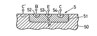
- FIG. 10 is a schematic cross-sectional view showing an example of a lateral bipolar transistor manufactured by such a CMOS process.
- the lateral bipolar transistor 5 is formed on the surface of the p-type semiconductor substrate 50.
- An n-well 51 is formed on the surface side of the p-type semiconductor substrate 50, and an n-rich portion 52 and two p-rich portions 53 and 54 are formed near the surface of the n-well 51.
- the base B is formed in the n-rich portion 52, the emitter E is formed in one p-rich portion 53, and the lateral collector (normal collector) C is formed in the other p-rich portion 54.
- PNP lateral bipolar is formed.
- the transistor 5 is configured. However, in this device structure, the p-type semiconductor substrate 50 itself becomes a parasitic collector and functions as a vertical collector C ′ of the transistor 5.
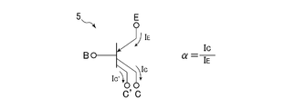
- the lateral bipolar transistor 5 is represented by a circuit symbol diagram as shown in FIG. 11, and an unnecessary current (parasitic collector current) I C 'flows through the vertical collector C'.
- the manufacturing error accounts for the absolute value of the current amplification factor ⁇ .
- the ratio increases, and the current amplification factor ⁇ tends to fluctuate due to the influence of the manufacturing error.
- the current amplification factor ⁇ also fluctuates with temperature.
- the multiplication core is a Gilbert multiplication core, but also in an analog multiplication circuit using a multiplication core consisting of a differential transistor pair consisting of a pair of emitter-coupled bipolar transistors. .
- a multiplication core consisting of a differential transistor pair consisting of a pair of emitter-coupled bipolar transistors.
- the present invention has been made to solve the above-mentioned problems, and lateral bipolar transistors manufactured by a CMOS process, bipolar junction transistors whose characteristics are not sufficiently good, etc. are used as bipolar transistors constituting a multiplication core.
- An object of the present invention is to prevent the deterioration of the calculation accuracy of an analog multiplication circuit by the multiplication core even when used.
- the detection accuracy of a detection circuit using an analog multiplication circuit having a multiplication core and the detection accuracy of a physical quantity sensor using the detection circuit are not reduced, or a variable gain amplifier using an analog multiplication circuit Another object is to prevent the amplification accuracy from being reduced.
- the analog multiplication circuit has at least one differential transistor pair consisting of a pair of emitter-coupled bipolar transistors, and the coupled emitter of the differential transistor pair is the first.
- a multiplying core having an input terminal, the two bases of the differential transistor pair as a second input terminal pair, and a collector of the differential transistor pair as an output terminal pair, and the second input terminal pair
- a linearization circuit having a linearization transistor pair consisting of a pair of bipolar transistors with emitters connected, and connecting each base and collector of the linearization transistor pair to a predetermined power supply, and the differential transistor pair A correction current is added to the second input terminal pair according to the current amplification factor of each bipolar transistor.
- a generation circuit characterized by comprising a.
- the correction current generation circuit includes a first replica transistor that is a replica of each bipolar transistor of the differential transistor pair, and the first bias transistor is supplied with a predetermined bias current to the emitter of the first replica transistor.
- the correction current may be generated based on the current obtained from the collector of the replica transistor.
- the correction current generation circuit further includes a second replica transistor that is a replica of each bipolar transistor of the linearization transistor pair, and the emitter of the second replica transistor is connected to the base of the first replica transistor.
- the collector and the base of the second replica transistor may be connected to a predetermined power supply.
- the multiplication core has two of the above differential transistor pairs, the coupled emitter of each of the two differential transistor pairs is taken as a first input terminal pair, and two bases are connected between the two differential transistor pairs. Are coupled to each other to form the second input terminal pair, and two collectors may be coupled to each other between the two differential transistor pairs to form the output terminal pair.
- the correction current generation circuit is a replica of the multiplication core and the linearization circuit, and first and second replica input terminals that are replicas of the first and second input terminals and the output terminal, and A replica multiplication unit having a replica output terminal, a comparison circuit comparing a trial output signal according to the output from the replica output terminal with an expected signal and outputting a comparison result signal, and the first and second replica input terminals A setting circuit for inputting a signal corresponding to a predetermined spare input value to the comparator and inputting the expectation signal corresponding to a predetermined expected value representing the product of the input values to the comparison circuit; And a correction current output circuit that generates a replica correction current that is a replica of the correction current and is added to the second replica input terminal pair, and the correction current output circuit It may be one that the trial output signal increases or decreases the correction current and the replica correction current in accordance with the comparison result signal so as to be equal to the expected signal.
- a variable gain amplifier includes any one of the above analog multiplication circuits in which the multiplication core has one of the above differential transistor pairs, a DC control signal is inputted to the first input terminal, and the second input is An input signal is input to the terminal, and a variable signal is obtained based on the output signal of the output terminal.
- a detection circuit includes any one of the above-mentioned analog multiplication circuits in which the multiplication core has two of the above-mentioned differential transistor pairs, and the amplitude at either the first input terminal or the second input terminal A constant alternating signal is input, a detected signal is input to the other, and a detected signal is obtained based on an output signal of the output terminal.
- a physical quantity sensor comprises a vibrator for converting a physical quantity applied from the outside into an electric signal, a reference signal generation circuit for outputting a reference signal, and an oscillation circuit for oscillating the vibrator based on the reference signal. And a detection circuit for detecting an output signal from the vibrator based on an oscillation signal from the oscillation circuit.
- the detection circuit is the detection circuit according to the present invention, the alternating signal is the oscillation signal, and the detection signal is an output signal from the vibrator.
- the correction current generation circuit may generate the correction current based on the reference signal.
- the correction current generation circuit generates a correction current that increases according to ⁇ , and adds the correction current to one input signal of the multiplication core to thereby bias the one input signal of the multiplication core.
- the current component (I 0 ) is corrected to the current ( ⁇ I 0 ) multiplied by the current amplification factor ( ⁇ ).
- Vout K ⁇ (Vx ⁇ Vy / I 0 ), and the output voltage Vout which is the multiplication result is not influenced by the current amplification factor ⁇ , and the multiplication is always performed with high accuracy. be able to.
- the detection circuit according to the present invention performs detection by analog multiplication using the alternating signal and the target signal as two input signals using the analog multiplication circuit according to the present invention, high-accuracy detection can always be performed.
- the variable gain amplifier according to the present invention can always perform variable amplification with high accuracy because it obtains a variable signal based on an output signal by analog multiplication of a control signal and an input signal using the analog multiplication circuit according to the present invention.
- a physical quantity sensor uses the detection circuit according to the present invention as an output signal according to a physical quantity externally applied by a vibrator as a target signal, and uses an oscillation signal for vibrating the vibrator as the alternating signal. Since the target signal is detected to detect the physical quantity, the physical quantity can always be detected with high accuracy.
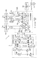
- FIG. 5 is a circuit diagram showing a configuration example of a correction current generation circuit in FIG. 3;
- FIG. 4 is a circuit diagram showing a configuration example of first and second VI conversion circuits in FIG. 3;
- FIG. 5 is a circuit diagram showing another example of an analog multiplication circuit according to the present invention and an embodiment of a variable gain amplifier. It is a block diagram of the analog multiplication circuit shown in FIG. FIG.
- FIG. 6 is a schematic block diagram illustrating yet another example embodiment of an analog multiplier circuit according to the present invention. It is a circuit diagram showing an example of the analog multiplication circuit which used the conventional Gilbert multiplication core.
- FIG. 2 is a schematic cross-sectional view showing an example of a lateral bipolar transistor manufactured by a CMOS process. It is a circuit symbol figure for demonstrating the current amplification factor of the lateral bipolar transistor produced by CMOS process.
- FIG. 1 First, one embodiment of an analog multiplication circuit and a detection circuit according to the present invention will be described with reference to FIG. In addition, in FIG. 1, the same code
- the analog multiplication circuit 1 shown in FIG. 1 includes an analog multiplication unit 100A and a correction current generation circuit 3.
- the configuration of the analog multiplication unit 100A includes a Gilbert multiplication core 101 and a linearization circuit 102, like the conventional analog multiplication circuit 100 described with reference to FIG.
- the four bipolar transistors Q1 to Q4 constituting the Gilbert multiplication core 101 of the analog multiplication unit 100A use lateral bipolar transistors manufactured by the CMOS process described in FIG. 10, bipolar junction transistors having poor characteristics, etc. doing.
- the bipolar transistors constituting the analog multiplication circuit 1 be elements of the same structure manufactured by the same manufacturing process, and have the same characteristics as possible.
- This can be realized by a known semiconductor layout technology, that is, a method of arranging many transistor elements of the same size and using adjacent elements among them.
- the absolute value of the transistor element characteristics and the amount of temperature change differ depending on the chip due to the error of the semiconductor manufacturing process, the relative positions of the elements used in the circuit can be considered by considering the geometrical arrangement in the chip in this way. Characteristics can be matched with high accuracy.
- the Gilbert multiplication core 101 has two differential transistor pairs each consisting of a pair of bipolar transistors emitter-coupled, and the coupled emitters of the two differential transistor pairs are taken as first input terminal pairs Ta and Tb. , The two differential transistor pairs are mutually coupled to each other to form second input terminal pairs Tc and Td, and the two differential transistor pairs are mutually coupled to each other between two collectors to be an output terminal It is the multiplication core which made the pair Te and Tf.
- the linearization circuit 102 has a linearization transistor pair consisting of bipolar transistors Q5 and Q6 whose emitters are respectively connected to the second input terminal pair Tc and Td of the differential transistor pair, and each of the linearization transistor pairs is It is an IV conversion circuit in which the base and each collector are connected to a predetermined power supply.
- the correction current generation circuit 3 is a circuit that generates a correction current in which the correction current corresponding to the current amplification factor ⁇ of each bipolar transistor Q1 to Q4 of the differential transistor pair is added to the second input terminal pair Tc and Td. .
- Voltage signal Vy which is an alternating signal having a constant amplitude is input to the VI conversion circuit 110 of the analog multiplication circuit shown in FIG. 1, and the amplitude changes at the same frequency as the voltage signal Vy to the VI conversion circuit 120.
- the analog multiplication circuit 1 can constitute a detection circuit.
- the analog multiplication circuit 1 outputs a voltage signal from the IV conversion circuit 150 as a detection signal according to the amplitude of the voltage signal Vx which is a detection signal.
- bipolar transistors hereinafter, “bipolar transistors” will be simply referred to as “transistors”) Q1 to Q4 forming the bi-differential circuit of the Gilbert multiplication core 101 will be specifically described.
- the Gilbert multiplication core 101 is composed of a first differential transistor pair 101a consisting of a pair of transistors Q1 and Q2 and a second differential transistor pair 101b consisting of a pair of transistors Q3 and Q4.
- the emitters of the transistors Q1 and Q2 are commonly connected to form one input terminal Ta of the first input terminal pair, and the emitters of the transistors Q3 and Q4 are commonly connected to each other to form the other of the first input terminal pair.
- Form the input terminal Tb of The bases of the transistors Q1 and Q4 are commonly connected to form one input terminal Tc of the second input terminal pair, and the bases of the transistors Q2 and Q3 are commonly connected to form the other input of the second input terminal pair.
- the terminal Td is formed.
- collectors of the transistors Q1 and Q3 are commonly connected to form one output terminal Te of the output terminal pair, and the collectors of the transistors Q2 and Q4 are commonly connected to form the other output terminal Tf of the output terminal pair doing.
- ⁇ I C / I E
- Is a circuit that generates a correction current of
- the transistors Q 1 to Q forming the Gilbert multiplication core 101 at the output voltage Vout of the Gilbert multiplication core 101 Remove the influence of the current amplification factor ⁇ of Q4.
- the transistor Q7 is a first replica transistor which is a bipolar transistor having the same current amplification factor ⁇ as the transistors Q1 to Q4 constituting the Gilbert multiplication core 101.
- the emitter of the transistor Q7 is connected to a positive power supply (+ V) through a constant current source 301, and the collector is connected to a negative power supply (-V) through a constant current source 302.
- a transistor Q8 diode-connected between the base of the transistor Q7 and the negative power supply (-V) is connected in the forward direction with respect to the direction in which the current flows.
- the transistor Q8 is preferably a second replica transistor that is a bipolar transistor having the same structure and characteristics as the transistors Q5 and Q6 that constitute the linearization circuit 102 of the analog multiplication unit 100A.
- the transistor element can also be realized by applying the above-described semiconductor layout technology.
- connection point p between the base of the transistor Q7 and the emitter of the transistor Q8 is connected to a positive power supply (+ V) through the constant current source 303, and the connection point q between the collector of the transistor Q7 and the constant current source 302 is It is connected to a positive power supply (+ V) through a diode-connected P-channel MOS transistor (hereinafter abbreviated as “PMOS”) 304.
- PMOS diode-connected P-channel MOS transistor
- the PMOS 305 is current-mirror connected to the PMOS 304 (that is, the gates and sources of the PMOS 304 and 305 are connected in common).
- the drain of the PMOS 305 is connected to a negative power supply (-V) via a diode-connected N-channel MOS transistor (hereinafter abbreviated as "NMOS") 306.
- NMOS diode-connected N-channel MOS transistor
- Two NMOSs 307 and 308 are current-mirror connected to the NMOS 306 (that is, the gates and sources of the NMOSs 306 to 308 are commonly connected). These current mirror circuits may be cascoded to increase the accuracy of the current copy.
- the respective drains of the two NMOSs 307 and 308 are connected to a positive power supply (+ V) via constant current sources 309 and 310 for supplying a constant current I 0 , respectively.
- the correction current output lines 311 and 312 are drawn from the connection points g and h of the drains of the NMOSs 307 and 308 and the constant current sources 309 and 310, respectively.
- the correction current output line 311 is connected to a connection point r between the input terminal Td of the Gilbert multiplication core 101 of the analog multiplication unit 100A, the emitter of the transistor Q5, and the positive output line of the VI conversion circuit 110.
- the correction current output line 312 is connected to a connection point s between the input terminal Tc of the Gilbert multiplication core 101, the emitter of the transistor Q6, and the negative output line of the VI conversion circuit 110.
- the constant current source 301 flows a second input terminal pair Tc of the Gilbert multiplier core 101, a constant current I 0 corresponding to the bias current of the differential current input to Td to the emitter of the transistor Q7, the thereby Gilbert multiplier core
- the current paths of the replicas of the current paths of the 101 transistors Q1 to Q4 are formed.
- the constant current I 0 a constant current source 303 corresponding to the bias current to flow to the emitter of diode-connected transistor Q8, thereby a replica of the current path of the transistors Q5, Q6 of the current path of the linearization circuit 102 It is formed.
- the emitter of the transistor Q7 is constant current flows I 0. Meanwhile, the current flowing in the collector of the transistor Q7, the constant current I 0, the base current and 10, reduced by the current amount flowing through the vertical collector C 'as described in FIG. 11, the current amplification factor at that time ⁇ current alpha ⁇ I 0 is the collector current in accordance with the flows into the connection point q. Since a constant current I 0 flows from the connection point q to the negative power supply (-V) by the constant current source 302, a current (1- ⁇ ) ⁇ I 0 is transmitted through the PMOS 304 from the positive power supply (+ V) to the connection point q. Flow.
- This current (1 ⁇ ) ⁇ I 0 is copied to the PMOS 305 which is current-mirror connected to the PMOS 304, and the current (1 ⁇ ) ⁇ I 0 flows also in the PMOS 305 and the NMOS 306 connected in series therewith. It is copied to the NMOSs 307 and 308, which are current-mirror connected to the NMOS 306, and the current (1- ⁇ ) ⁇ I 0 also flows through them.
- the current ⁇ ⁇ I 0 which is the two correction currents, flows into the above-mentioned connection points r and s of the analog multiplication unit 100A by the correction current output lines 311 and 312, and is output from the VI conversion circuit 110 ⁇ K1 -It is added to Vy.
- the differential current flowing from the connection points r and s to the transistors Q5 and Q6 of the linearization circuit 102 becomes ⁇ ⁇ I 0 ⁇ K1 ⁇ Vy.
- a constant current I 0 which is a bias current of a differential current for input to each input terminal Tc, Td of the second input terminal pair of the Gilbert multiplication core 101 is a current ⁇ ⁇ I multiplied by a current amplification factor ⁇ It is corrected to 0 .
- the differential current ( ⁇ ⁇ I 0 ⁇ K1 ⁇ Vy) is converted by the linearization circuit 102 into a voltage signal Vi given by the following equation, and is input to each input terminal Tc, Td of the second input terminal pair Be done.
- Vi 2 ⁇ V T ⁇ tan h -1 (K 1 ⁇ V y / ( ⁇ ⁇ I 0 ))
- Vout K ⁇ ⁇ Vx ⁇ Vy / ( ⁇ ⁇ I 0 ) ⁇ ⁇ ⁇
- Vout K ⁇ (Vx ⁇ Vy / I 0 )
- the output voltage Vout which is the multiplication result is not influenced by the current amplification factor ⁇ , and the multiplication can always be performed with high accuracy.
- the voltage signal (output voltage Vout) output from the IV conversion circuit 150 corresponds to the amplitude of the voltage signal Vx which is a detected signal.
- the detection signal can be accurately obtained without being affected by the current amplification factor ⁇ of the transistors Q1 to Q4 constituting the Gilbert multiplication core 101.
- each bipolar transistor Q1 to Q8 in this analog multiplication circuit 1 uses all PNP type, the operation principle is the same even if the NPN type bipolar transistor is used, only the direction of the current is reversed. It is the same.
- FIG. 2 to FIG. 5 An embodiment of a physical quantity sensor and a detection circuit according to the present invention using the above-described analog multiplication circuit will be described with reference to FIGS.
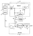
- FIG. 2 First, the entire configuration of an embodiment of the physical quantity sensor according to the present invention will be described with reference to FIG.
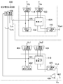
- the physical quantity sensor shown in FIG. 2 is a vibration-type angular velocity sensor composed of a sensor element 10, an oscillation circuit 20, a detection circuit 30, and a reference signal generation circuit 40.
- the sensor element 10 is, for example, a gyro vibrator for detecting a rotational angular velocity, in which a metal electrode is disposed on the surface of a piezoelectric material formed in a tuning fork shape, and includes a drive unit 11 and a detection unit 12.
- the sensor element 10 is driven to oscillate by the oscillation circuit 20, and when a rotational angular velocity is received during its oscillation, the sensor section 10 outputs a weak alternating current signal as the sensor element output S12 from the detection unit 12.
- the reference signal generation circuit 40 is a circuit that generates a reference signal for an AGC control circuit described later, and here is a constant voltage circuit that generates a reference signal S41 that is a substantially constant voltage that does not depend on ambient temperature or power supply voltage. Use.
- the oscillation circuit 20 forms an oscillation loop for the sensor element 10 by the monitor circuit 21 and the variable gain amplifier 22 and is an oscillation circuit having a so-called AGC function. Therefore, the oscillation circuit 20 includes the AGC control circuit 23, and has a function of controlling the gain of the variable gain amplifier 22 so that the effective value of the excitation current of the sensor element 10 becomes equal to the reference signal S41.
- the oscillation circuit 20 converts the excitation current of the sensor element 10 into a voltage signal by the monitor circuit 21.
- oscillation control of the sensor element 10 is performed by the AGC control circuit 23, and the oscillation signal S21 output from the monitor circuit 21 becomes an AC signal having an amplitude based on the reference signal S41.
- the oscillation signal S21 is also used as a signal used for multiplication in the detection circuit 32 described later.
- the detection circuit 30 is configured of an amplification circuit 31, a detection circuit 32, and a filter circuit 33.
- the amplification circuit 31 amplifies a sensor element output S12, which is an output signal from the detection unit 12 of the sensor element 10.
- the detection circuit 32 detects an angular velocity signal component included in the amplified signal S31 which is an output signal of the amplification circuit 31.
- the filter circuit 33 amplifies and smoothes the output signal S32 of the detection circuit 32 (that is, the detection signal), and outputs the amplified signal as an output signal S30 of the physical quantity sensor.
- the detection circuit 32 includes an analog multiplication circuit which analogically multiplies the amplification signal S31 which is an output signal of the amplification circuit 31 and the above-mentioned oscillation signal S21, and utilizes the above-mentioned analog multiplication circuit.
- the oscillation circuit 20 and the detection circuit 30 are integrated circuits that operate by being connected to a positive power supply (+ V) and a negative power supply (-V), and can be configured on the same semiconductor substrate.
- trigonometric function means that the above multiplication yields two components of a signal of twice the frequency of the original signal and a DC signal. It is understood from the nature.
- a DC signal of magnitude A ⁇ B / 2 can be obtained.
- the oscillation signal S21 and the amplification signal S31 are both signals of the same frequency. For example, if a signal in which A is substantially constant and a signal in which B is proportional to the rotational angular velocity to be applied are selected, and a calculation operation represented by the above equation is performed, a signal proportional to the rotational angular velocity is obtained.
- Be The detection circuit 32 described next performs detection using this principle.
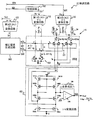
- FIG. 3 Next, the configuration of the detection circuit 32 in the physical quantity sensor shown in FIG. 2 will be described using FIG. In FIG. 3, parts corresponding to those in FIGS. 1 and 9 are denoted with the same reference numerals, and redundant description thereof will be omitted.
- the detection circuit 32 is an analog multiplication including first, second and third V-I conversion circuits 110, 120 and 130, constant current sources 2c and 2d, an analog multiplication unit 100A and a correction current generation circuit 300.
- a circuit 1A, an IV conversion circuit 150, and a phase shift circuit 160 are provided.
- the detection circuit 32 includes a first VI conversion circuit 110 and a second VI conversion circuit 120 (VI conversion circuit in FIG. 1 for converting the oscillation signal S21 and the amplification signal S31 into current signals, respectively. (Same as 110, 120).
- the output format of these VI conversion circuits is that of differential output. The configuration of the first and second V-I conversion circuits 110 and 120 will be described later.
- the oscillation signal S21 is input to the first VI conversion circuit 110 via the phase shift circuit 160. This is to align the phases of the signals to be multiplied, as in the multiplication detection equation described above.
- the signal phase-adjusted by the phase shift circuit 160 is represented as an oscillation signal S21 '.
- the oscillation signal S21 ' is a sine wave alternating signal whose amplitude is controlled to be constant by the operation of the AGC control circuit 23 described above, and corresponds to the input signal according to the voltage signal Vy in FIGS.
- the voltage value of the oscillation signal S21 ' is represented as Vy.
- the first VI conversion circuit 110 converts the oscillation signal S21 'of the voltage value Vy into a differential current ( ⁇ K1 ⁇ Vy) with a conversion coefficient K1 and outputs it.
- the amplified signal S31 input to the second VI conversion circuit 120 is a sine wave to-be-detected signal vibrating at the same frequency as the oscillation signal S21 'which is an alternating signal, and is determined by the voltage signal Vx in FIGS. Since the voltage corresponds to the input signal, the voltage value of the amplified signal S31 is represented as Vx in the symbol indicating the value of the differential current below.
- the second VI conversion circuit 120 converts the amplified signal S31 of the voltage value Vx into a differential current ( ⁇ K2 ⁇ Vx) with a conversion coefficient K2 and outputs it.
- the constant current sources 2c and 2d add a bias current Ib to the differential current (. +-. K2.Vx) output from the second V-I conversion circuit 120 to generate a differential current (Ib. ⁇ .K2) including the bias current. ⁇ Set to Vx).
- constant current sources 2c and 2d are shown separately from the second V-I conversion circuit 120 for convenience of explanation, these constant current sources may be provided in the second V-I conversion circuit 120. These constant current sources may be referred to as a VI conversion circuit which converts an input signal into a differential current including a bias current.
- the output current Ir is equivalent to the constant current I 0 by the constant current source 301 and the like in the correction current generating circuit 3 in FIG. 1, changes according to a voltage value Vr of the reference signal S41.
- the correction current generation circuit 300 biases one input signal so that the multiplication result does not change even if the current amplification factor ⁇ of the bipolar transistors Q1 to Q4 constituting the Gilbert multiplication core 101 changes due to temperature or the like. It is a circuit for correcting the current value.
- the correction current generation circuit 300 in this embodiment has a current amplification factor ⁇ equal to the current amplification factor ⁇ of the bipolar transistors Q1 to Q4 constituting the Gilbert multiplication core 101 in the output current Ir of the third V-I conversion circuit 130.
- the corrected current ⁇ ⁇ Ir is output from the corrected current output lines 321 and 322 and added to the connection points r and s of the analog multiplication unit 100A. The details will be described later with reference to FIG.
- the IV conversion circuit 150 is a circuit that converts the output signal I4 by the differential current from the analog multiplication unit 100A of the analog multiplication circuit 1A into a voltage signal with a conversion coefficient K5.
- the IV conversion circuit 150 shown in FIG. 3 converts a differential current input into a single-phase current signal by a so-called folded cascode circuit of PMOS 151A, 151B, 152A, 152B and NMOS 153A, 153B, 154A, 154B, and further converts it.
- An IV conversion is performed by the resistor 156 and the operational amplifier 155 to output the output voltage Vout according to the amplitude of the signal to be detected.
- reference signal S41 (voltage value) is used as a bias current to be added to the differential current ( ⁇ K1 ⁇ Vy) obtained by converting the input signal by voltage signal Vy which is oscillation signal S21 ′ by first VI conversion circuit 110.
- the reason for using the current ( ⁇ ⁇ Ir) according to Vr) will be described.
- an alternating signal having the same frequency as the detected signal and having a constant amplitude is required.
- AGC control is performed in which the excitation level of the oscillator is controlled to a constant level based on a reference signal using a constant voltage circuit or the like, so the controlled oscillation signal is It is used as an alternating signal for multiplication.
- the reference signal changes with temperature change.
- the amplified signal S31 obtained by amplifying the sensor element output S12 which is a detected signal is also proportional to the excitation level of the sensor element 10 which is a vibrating body in addition to the angular velocity, so the detected signal (amplified signal S31) and the oscillation signal are simply used.
- the oscillation signal S21 'obtained by phase-adjusting S21 is multiplied, a component obtained by squaring the reference signal S41 appears in the detection output signal (output voltage Vout). Therefore, a large error occurs in the detection output signal due to the error of the reference signal. This becomes an obstacle to achieving high accuracy in a wide operating temperature range, which is required for physical quantity sensors in recent years.
- the third V-I conversion circuit 130 which receives the reference signal S41 as described above, the output current Ir thereof and one of the input signals of the analog multiplication unit 100A. And a summing circuit for summing the differential current ( ⁇ K1 ⁇ Vy). This reduces the fluctuation of the output signal due to the voltage fluctuation of the reference signal.
- the analog multiplication unit corrects the current ⁇ ⁇ Ir obtained by correcting the output current Ir by the correction current generation circuit 300. It is considered as the addition current to one input signal of 100A.
- the negative output current (inverted output current) (-K1.Vy) of the first V-I conversion circuit 110 is applied to the emitter of the other transistor Q6 constituting the linearization circuit 102 as well as the reference signal S41.
- the above-described addition circuit corresponds to a portion that generates a sum of each output current of the first V-I conversion circuit 110 and each output current of the correction current generation circuit 300.
- the connection at the connection point r between the output terminals of the VI conversion circuit 110 and the correction current generation circuit 300 and the connection point s corresponds to the addition circuit. This is because the addition of current signals can be performed by wire connection.
- the transistors Q5 and Q6 are both diode-connected, and their bases and collectors are connected to a negative power supply (-V).
- the emitter of the transistor Q5 is connected to an input terminal Tc in which the bases of the transistors Q1 and Q4 of the Gilbert multiplication core 101 are connected to each other.
- the emitter of the transistor Q6 is connected to the input terminal Td in which the bases of the transistors Q2 and Q3 of the Gilbert multiplication core 101 are connected to each other.
- the current (Ib-K2 ⁇ Vx) to which the bias current Ib is added is configured to flow.
- the bias current Ib is generated by constant current sources 2c and 2d which are bias current sources.
- the bias current Ib and the output current Ir of the VI conversion circuits 120 and 130 are provided for the purpose of preventing the current flowing through the bipolar transistor of the multiplication core from becoming negative and cutting off regardless of whether the input signal is positive or negative. In addition to the output current. Therefore, the value of the bias current Ib is set according to the range of the detected signal which is the input signal, that is, the voltage signal Vx.
- An output terminal pair that outputs a signal I4 is configured.
- the IV conversion circuit 150 converts the differential current output from the output terminal pair Te, Tf into a voltage signal as described above, and outputs an output voltage Vout.
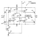
- FIG. 4 The configuration and operation of the correction current generation circuit 300 in FIG. 3 will be described with reference to FIG.
- the correction current generation circuit 300 shown in FIG. 4 has a basic configuration in common with that of the correction current generation circuit 3 in FIG. 1, and the same reference numerals are given to the common portions, and detailed descriptions thereof will be omitted. Do.
- the output current Ir of the third V-I conversion circuit 130 is replaced with the constant current I 0 by the constant current source 301 in the correction current generation circuit 3 of FIG. Flow to the emitter.
- the base of the transistor Q7 is connected to the connection point p between the emitter of the diode-connected transistor Q8, which is a second replica transistor, and the constant current source 303, as in the correction current generation circuit 3.
- the difference from the correction current generation circuit 3 is that the PMOS 304 and PMOS 305 connected in the current mirror in the correction current generation circuit 3 in FIG. 1 are changed to a cascoded current mirror circuit to improve the accuracy of current copy. .
- the current mirror circuit cascode-connects the PMOS 315A, 316A and the NMOS 317A between the positive power supply (+ V) and the connection point q between the collector of the transistor Q7 and the constant current source 302, and cascode connection to each of these MOS transistors
- the PMOSs 315B and 352B and the NMOS 317B are connected in a current mirror manner.
- the source of the NMOS 317 B is connected to the negative power supply ( ⁇ V) through the NMOS 306.
- the NMOSs 307 and 308 are current-mirror connected to the NMOS 306.
- the correction current output lines 321 and 322 are drawn from the connection point g of the drain of the NMOS 307 and the constant current source 309 and the connection point h of the drain of the NMOS 308 and the constant current source 310, respectively.
- the collector current of ⁇ ⁇ Ir according to the current amplification factor ⁇ ( ⁇ ⁇ 1) of the transistor Q7 is Flow.
- the collector current flows into a connection point q between the collector of the transistor Q7 and the source of the NMOS 317A, and a constant current I 0 flows from the connection point q to the negative power supply (-V).
- the current (I 0 - ⁇ ⁇ Ir) flows in the series circuit of the NMOS 317A.
- PMOS315B, 316B and NMOS317B, 306 also the same amount of current (I 0 - ⁇ ⁇ Ir) flows in the series circuit of, NMOS306 and is current-mirror-connected, current to NMOS307,308 (I 0 - ⁇ ⁇ Ir) flows.
- VI conversion circuit 110 and the second VI conversion circuit 120 used for the detection circuit 32 shown in FIG. 3 will be described with reference to FIG.
- These VI conversion circuits are transconductance amplifiers having the same configuration and utilizing MOS transistors and resistance elements, and PMOS 201 to 207, NMOS 211 to 217, conversion resistor 220, and tail current source 230. It is composed of
- the gate terminal of the PMOS 202 is the input terminal IN of the VI conversion circuit.
- the PMOSs 201 and 202, the NMOSs 211 and 212, and the tail current source 230 form a differential pair circuit with the PMOSs 201 and 202 as input elements and the NMOSs 211 and 212 as load elements.
- the gate terminal of the PMOS 202 corresponds to the non-inversion input terminal of the differential pair circuit
- the gate terminal of the PMOS 201 corresponds to the inversion input terminal
- the bias current is supplied to the differential pair circuit by the tail current source 230.
- the NMOS 211 and the NMOS 212 are respectively diode-connected, and the current value flowing to the NMOS 212 is copied to the NMOS 214 by a predetermined value times the current mirror, and the current value flowing to the NMOS 211 is copied to the PMOS 204 via the NMOS 213 and the PMOS 203 by a predetermined value .
- the drain terminals of the PMOS 204 and the NMOS 214 are connected to each other, and the gate terminal of the PMOS 201 corresponding to the inverting input terminal and one end of the conversion resistor 220 are connected to this terminal.
- the other end of the conversion resistor 220 is grounded to the signal ground.
- the conversion resistor 220 is formed of a linear resistive element such as a polysilicon resistor.
- the current value flowing to the PMOS 204 is copied to the PMOS 207 by current mirror connection
- the current value flowing to the NMOS 214 is copied to the NMOS 217 by current mirror connection.
- the drain terminals of the PMOS 207 and the NMOS 217 are connected to each other, and the output terminal IOUT is provided at the connection point.
- the current value flowing to the NMOS 211 is copied to the NMOS 216 by a predetermined value multiple by a current mirror, and the current value flowing to the NMOS 212 is copied to the PMOS 206 via the NMOS 215 and the PMOS 205 by a predetermined value.
- the drain terminals of the PMOS 206 and the NMOS 216 are connected to each other, and the inverting output terminal IOUTB is provided at the connection point.
- the PMOSs 201 to 204 and the NMOSs 211 to 214 operate as voltage followers in which one end on the non-ground side of the conversion resistor 220 is regarded as an output, and the same signal as the signal input to the input terminal IN is the conversion resistor. It appears at one end of 220. Further, the current flowing to the conversion resistor 220 is copied by the remaining MOS transistors, and a current obtained by dividing the input signal voltage by the resistance value of the conversion resistor 220 is output from the output terminal IOUT. Then, from the inverting output terminal IOUTB, a current whose absolute value is equal to that of the current output from the output terminal IOUT and whose direction is opposite to that of the current is output.
- K in the above equation is a conversion coefficient (different from K in the equation of the output voltage Vout in FIGS. 9 and 1), and is the inverse of the resistance value of the conversion resistor 220.
- this conversion coefficient is K1
- this conversion coefficient is K2.
- the double sign “ ⁇ ” corresponds to the output current of the output terminal (positive output terminal) and the inverting output terminal (negative output terminal), respectively.
- the V-I conversion circuit described here is a configuration used for the first V-I conversion circuit 110 and the second V-I conversion circuit 120 in FIG. Although the configuration of the third VI conversion circuit 130 is not particularly shown, a single-ended output eliminates the need for a circuit for copying the current value flowing through the PMOS 207 and the NMOS 217 by current mirror connection and the inverting output terminal IOUTB.
- the reference signal generation circuit 40 When positive and negative power supply voltages are applied to the physical quantity sensor shown in FIG. 2, the reference signal generation circuit 40 outputs the reference signal S41, and the oscillation circuit 20 drives the sensor unit 10 with a predetermined current value based on the reference signal S41. AC drive. At that time, since AGC control is performed, an alternating voltage having an amplitude based on the reference signal S41 is output as the oscillation signal S21.
- the detection circuit 30 When the rotational angular velocity is applied to the physical quantity sensor in this state, an AC signal having an amplitude corresponding to the rotational angular velocity appears at the sensor element output S12.
- the detection circuit 30 amplifies this sensor element output S12 and converts it into a voltage signal, and inputs it to the detection circuit 32 as an amplified signal S31.
- the reference signal S41 and the oscillation signal S21 are further input to the detection circuit 32.
- the detection circuit 32 performs analog multiplication detection as described below, and smoothing processing is performed by the filter circuit 33 at the next stage. As a result, the physical quantity sensor outputs from the filter circuit 33 an output signal S30 of a voltage proportional to the applied rotational angular velocity.
- the voltage value of the oscillation signal S21 'obtained by phase-adjusting the oscillation signal S21 by the phase shift circuit 160 is Vy
- the voltage value of the amplification signal S31 is Vx
- the voltage value of the reference signal S41 is Vr.
- Vy and Vx are sinusoidal signals (expressed in the form of A ⁇ sin ⁇ ) at the same frequency and in the same phase.
- the double sign “ ⁇ ” corresponds to positive and negative of the differential current signal.
- I4 ⁇ (K1 ⁇ K2) ⁇ (Vx ⁇ Vy) / ( ⁇ ⁇ Ir) ⁇ ⁇ ⁇
- the current amplification factor ⁇ of the bipolar transistors Q1 to Q4 constituting the Gilbert multiplication core 101 is canceled by the numerator and the denominator, so that the influence is eliminated. Therefore, even if using a transistor such as a lateral bipolar transistor manufactured by a CMOS process in which current amplification factor ⁇ fluctuates due to temperature etc. for these elements, accurate detection output can be obtained without being affected by it. Can.
- Vout ⁇ 2 ⁇ (R3 ⁇ R5 ⁇ K1 ⁇ K2) ⁇ (Vx ⁇ Vy) ⁇ / Vr
- Vy in the above equation is the voltage value of the oscillation signal S21 ', it is the same as the voltage value of the oscillation signal S21.
- the oscillation signal S21 is a signal whose oscillation amplitude is controlled by the AGC control circuit 23 in FIG. 2 and depends (proportional) on the voltage value Vr of the reference signal S41 which is the reference of AGC control (Vy ⁇ Vr).
- Vx is a voltage value of an amplified signal S31 obtained by amplifying the angular velocity signal obtained from the detection unit 12 of the sensor element 10. Therefore, this amplified signal S31 is proportional to the intensity of the applied angular velocity, but also proportional to the intensity for exciting the drive portion 11 of the sensor element 10 to detect the angular velocity. That is, it is also proportional to the voltage value Vr of the reference signal S41 (Vx ⁇ Vr).
- the output signal S30 of the physical quantity sensor in which the output voltage Vout is smoothed by the filter circuit 33 shown in FIG. 2 is also simply proportional to the voltage value Vr.
- the physical quantity sensor of this embodiment has an advantage of using analog multiplication detection in addition to the characteristic. There is. That is, since the signal component to be detected in the physical quantity sensor of this embodiment is only the same frequency component as the oscillation frequency, noise having other frequency components due to external vibration etc. is temporarily included in the detected signal Also, the noise component is frequency-converted to a frequency sufficiently higher than DC by analog multiplication detection, and can be easily removed by the filter circuit 33 at the next stage.
- K1, K2, K3 included as a factor in the K 0 is a conversion coefficient of each V-I conversion circuit 110, 120 and 130, the transform coefficient as in this embodiment, the conversion resistor by linear resistance element
- the resistance based on the resistance value it is also possible to offset the temperature coefficient, the semiconductor process fluctuation, and the like between the conversion coefficient K3 and the conversion coefficient K1 or K2.
- the temperature coefficient and the semiconductor process fluctuation are offset between the resistance value R5 and the conversion factor K2 or K1. Will also be possible.
- Vout 2 ⁇ ⁇ (R3 ⁇ R5) / (R1 ⁇ R2) ⁇ ⁇ ⁇ (Vx ⁇ Vy) / Vr ⁇
- the configuration in which the component of the reference signal is added to the input of the analog multiplication circuit is a method of current addition in which the current signal generated by the VI conversion from the reference signal and the input signal of multiplication is added.
- the same effect as that of the present embodiment can be obtained by adding a reference signal and an input signal of multiplication in the state of a voltage signal and then performing a voltage addition method in which a VI conversion is performed.
- the addition of voltage signals can be performed by a well-known voltage addition circuit using an operational amplifier and a resistor.
- the reference signal used for AGC control is a voltage signal, but if the reference signal is a current signal, it is apparent that the third VI conversion circuit 130 is unnecessary. is there.
- the reference signal is added to the oscillation signal obtained from the drive circuit of the sensor element which is one of the two input signals to be multiplied, but the opposite may be applied. That is, the reference signal may be added to the amplified signal obtained by amplifying the sensor element output which is the other of the two input signals, and the added signal and the oscillation signal may be input to the multiplication core.
- the same operation as the above embodiment is performed. This is also apparent from the fact that the multiplication order is interchangeable.
- the current ⁇ ⁇ I 0 which is two correction currents in FIG.
- the correction current generation circuit 3 can also be used.
- the output voltage Vout which is the multiplication result of the voltage signals Vx and Vy is not influenced by the current amplification factor ⁇ . Then, a detection signal according to the amplitude of the voltage signal Vx which is a detection signal can be accurately obtained without being affected by the current amplification factor ⁇ of the transistors Q1 to Q4 constituting the Gilbert multiplication core 101.
- FIG. 6 Another Example of Analog Multiplication Circuit and Embodiment of Variable Gain Amplifier: FIG. 6
- FIG. 6 parts corresponding to FIG. 3 are given the same reference numerals, and the description thereof will be omitted.
- the analog multiplication circuit 1B in this embodiment includes an analog multiplication unit 100B and a correction current generation circuit 3.
- the analog multiplication unit 100 B is configured of a multiplication core 105 and a linearization circuit 102.
- the multiplication core 105 is a differential transistor pair consisting of transistors Q1 and Q2 which are a pair of emitter-coupled bipolar transistors, and the coupled emitter of the differential transistor pair is the first input terminal Ta, and the bases of these transistors are Let Tc be a second input terminal pair Tc, Td, and let the collectors of those transistors be an output terminal pair Te, Tf.
- the multiplication core 105 is not a Gilbert multiplication core.
- the correction current generation circuit 3 is the same circuit as the correction current generation circuit 3 described with reference to FIG. 1 and has a constant current I 0 as a first replica transistor having the same characteristics as the transistors Q1 and Q2 constituting the multiplication core 105. It corrects with the current amplification factor ⁇ of Q7, and outputs two systems of correction current (which also serves as a bias current) ⁇ ⁇ I 0 .
- variable gain amplifier 42 of this embodiment is configured to receive the gain of the input signal Si (voltage value Vy) input to the second input terminal 43 and the DC control signal Sc (voltage value input to the first input terminal 44. It is a circuit controlled according to Vx).
- an IV conversion circuit 150 for converting an output signal into a voltage signal.
- the second VI conversion circuit 120A is a circuit obtained by removing the inversion output terminal IOUTB and the circuit for generating the inversion output current from the VI conversion circuit shown in FIG.
- the output current Ix from the second V-I conversion circuit 120 A is input to the first input terminal of the multiplication core 105.
- the differential current ( ⁇ Iy) from the first VI conversion circuit 110 and the current ⁇ ⁇ I 0 that is the correction current from the correction current generation circuit 300A are added, and the differential current of the addition result is a linearization circuit
- the signal is converted into a differential signal having a voltage difference corresponding to the voltage signal Vi by 102, and the differential signal is input to the second input terminal pair of the multiplication core 105.
- the IV conversion circuit 150 provides, as an output voltage Vout, a voltage signal obtained by amplifying the input signal Si with a gain controlled by the control signal Sc.
- the voltage difference applied to the second input terminal pair Tc, Td formed of the bases of the transistors Q1, Q2 is Vi.
- the base current of the transistor Q1 is I B1
- the collector current is I C1
- the base current of the transistor Q2 is I B2
- the collector current is I C2
- the following equation is established.
- V T is a so-called heat voltage.
- the output current Ix flowing into the first input terminal Ta of the multiplier core 105 from the second V-I converting circuit 120A is the sum of the emitter currents I E1, I E2 of the transistors Q1, Q2, the following equation To establish.
- the transistors Q5 and Q6 of the linearization circuit 102 are diode-connected, assuming that the emitter voltage of the transistor Q5 is V1 and the inter-emitter voltage of the transistor Q6 is V2, the following equation is established. Is is a so-called reverse saturation current.
- the output voltage Vout of the IV conversion circuit 150 is obtained by the following equation, where R5 is the resistance value of the conversion resistor 156.
- the output voltage Vout is proportional to Vx ⁇ Vy. That is, the output voltage Vout which is the multiplication result of the voltage signals Vx and Vy is not influenced by the current amplification factor ⁇ of the transistors Q1 and Q2 constituting the multiplication core 105, and the multiplication can always be performed with high accuracy.
- the output voltage Vout which is a voltage signal obtained by amplifying the input signal Si by the gain controlled by the control signal Sc, is equal to the current amplification factor ⁇ of the transistors Q1 and Q2 constituting the multiplication core 105. It can be obtained precisely without being affected.
- variable gain amplifier 42 as the variable gain amplifier 22 of the oscillation circuit 20 in the physical quantity sensor shown in FIG.
- the analog multiplication circuit As described above, the analog multiplication circuit according to the present invention generates the correction current which increases according to the current amplification factor ⁇ of the transistor of the analog multiplication section by the correction current generation circuit, and the correction current is used as one of the multiplication cores. It has a feature related to the circuit configuration in that it is added to the input signal, so that even if the current amplification factor ⁇ of the transistor that constitutes the analog multiplication unit fluctuates due to temperature etc., the multiplication result is not affected by the fluctuation can get.
- FIG. 7 is a block diagram of the analog multiplication circuit shown in FIG.
- the correction current generation circuit 3 increases according to ⁇ using the transistor Q7 which is a replica transistor of the transistors Q1 to Q4 and the transistor Q8 which is a replica transistor of the transistors Q5 and Q6. Generate ⁇ ⁇ I 0 as a correction current.
- the circuit configuration of such a correction current generation circuit 3 is an example of a circuit that generates a correction current, and the analog multiplication circuit according to the present invention generates another correction current that increases according to the current amplification factor ⁇ .
- a correction current generation circuit can also be used.
- FIG. 8 is a schematic block diagram of an example of an analog multiplication circuit using a correction current generation circuit having a circuit configuration different from that of the correction current generation circuit 3.
- the same components as those described above are denoted by the same reference numerals, and redundant description thereof will be omitted.
- the correction current generation circuit 400 of this embodiment includes a replica multiplication core 401, a replica linearization circuit 402, a first input current generation circuit 403, a second input current generation circuit 404, an IV conversion circuit 405, and a comparator 406. , And an expected signal input circuit 407 and a correction current output circuit 408.
- the replica multiplication core 401 is a replica of the multiplication core 105 and has the same circuit configuration as the multiplication core 105, and the first and second input terminal pairs of the multiplication core 105 and the first and second corresponding to the output terminal pair. , And a replica output terminal pair. Also, the transistors forming the replica multiplication core 401 are replica transistors having the same current amplification factor ⁇ as the transistors Q1 to Q4 forming the multiplication core 105.
- the replica linearization circuit 402 is a replica of the linearization circuit 102. That is, replica linearization circuit 402 is diode-connected (ie, the base and the collector are directly connected) between each terminal of the second replica input terminal pair of replica multiplication core 401 and the negative power supply (-V). 2.) A pair of bipolar transistors, which are linearizing transistors, are connected in the forward direction with respect to the direction in which the current flows. The pair of bipolar transistors constituting the replica linearization circuit 402 are replica transistors having the same characteristics as the transistors Q5 and Q6 constituting the linearization circuit 102.
- the replica multiplication core 401 and the replica linearization circuit 402 constitute an analog multiplication unit 410 (replica multiplication unit) which is a replica of the analog multiplication unit 100A.
- the first input current generation circuit 403, the second input current generation circuit 404, and the expectation signal input circuit 407 input signals corresponding to a predetermined spare input value to the first and second replica input terminals respectively, and A setting circuit is configured to input an expected signal corresponding to a predetermined expected value representing the product of the input values to the comparator 406.
- the first input current generation circuit 403 can be a VI conversion circuit that converts a predetermined input voltage Vu1 into a differential current, and the differential current is a second replica input terminal of the replica multiplication core 401 Supplied in pairs.
- the second input current generation circuit 404 can be a VI conversion circuit that converts a predetermined input voltage Vu2 into a differential current, and the differential current is a first replica of the replica multiplication core 401. It is supplied to the input terminal pair.
- the VI conversion circuits constituting the first and second input current generation circuits 403 and 404 have the same circuit configuration as the VI conversion circuits 110 and 120, respectively.
- the first and second input current generation circuits 403 and 404 receive the input voltages Vu1 and Vu2 from the outside.
- the first and second input current generation circuits 403 and 404 may generate predetermined input voltages Vu1 and Vu2 inside them, and convert the voltages into VI.
- the expectation signal input circuit 407 inputs, to the comparator 406, an expectation signal corresponding to the product of the input values represented by the input voltages Vu1 and Vu2.
- the expectation signal is a signal representing the expected value of the output value given by the replica multiplication core 401 to the input voltages Vu1 and Vu2.
- the expectation signal input circuit 407 is a terminal connected to the input of the comparator 406 and externally applied with the voltage Vs.
- the voltage Vs is generated by a user or the like based on the input voltages Vu1 and Vu2, and is applied to the terminal.
- the expectation signal input circuit 407 may be a circuit that generates the voltage Vs based on a signal input from the outside. Further, the expectation signal input circuit 407 may be a circuit that internally generates, as an expectation signal, a voltage Vs that is predetermined corresponding to the predetermined input voltages Vu1 and Vu2.
- the IV conversion circuit 405 and the comparator 406 compare the trial output signal corresponding to the differential current output by the replica multiplication core 401 as the multiplication result of the input values represented by the input voltages Vu1 and Vu2 with the expected signal and compare the comparison result
- the comparator circuit which outputs a signal is comprised.
- the IV conversion circuit 405 converts the differential current output from the replica multiplication core 401 into a voltage Vu 3 which is a trial output signal, and inputs it to the comparator 406.
- the comparator 406 compares the voltage Vu3 with the voltage Vs, and outputs a comparison result signal indicating the magnitude relationship between them.
- the correction current output circuit 408 generates a correction current I CR1 and a replica correction current I CR2 which is a replica of the correction current.
- the correction current I CR1 is a correction current to be added to the second input terminal pair of the multiplication core 105 as in the above-described embodiment.
- replica correction current I CR2 is added to the second replica input terminal pair of replica multiplication core 401. Two systems each of the correction current I CR1 and the replica correction current I CR2 are generated, and the current values of the four systems are identical.
- the correction current output circuit 408 increases or decreases the replica correction current I CR2 according to the comparison result signal so as to equalize the voltage Vu3 as the trial output signal to the voltage Vs as the expectation signal, and the same as the replica correction current I CR2 A magnitude correction current I CR1 is generated.
- the correction current generation circuit 400 is an analog multiplication that is a replica of the analog multiplication unit 100A, even if the current amplification factor ⁇ of the transistor of the analog multiplication unit 100A including the multiplication core 105 and the linearization circuit 102 changes.
- a feedback control is performed on replica correction current I CR2 so that unit 410 gives a correct result, and the result of the feedback control is added as the correction current I CR1 to the second input terminal pair of multiplication core 105, thereby obtaining analog multiplication unit 100A.
- the correction current generation circuit 400 of this embodiment can obtain a multiplication result from which the influence of fluctuation other than the current amplification factor ⁇ is removed.
- the analog multiplication circuit shown in FIG. 8 can also be used, for example, in a detection circuit of a physical quantity sensor as shown in FIG.
- the detection circuit of FIG. 2 by setting the correction current to a current value proportional to the voltage value Vr of the reference signal, the output voltage when the voltage values of the voltage signals Vx and Vy are proportional to the voltage value Vr of the reference signal It has been described above that the Vr dependence of Vout can be reduced (it remains proportional to Vr).
- correction current output circuit 408 corrects the voltage proportional to voltage value Vr. The current is output, thereby obtaining the above-described effect of suppressing the occurrence of the fluctuation of the reference signal in the output voltage Vout of the physical quantity sensor.
- the analog multiplication circuit according to the present invention can also be used as a general detection circuit or a detection circuit in a physical quantity sensor other than an angular velocity sensor.
- the input of the reference signal as in the embodiment shown in FIG. 3 may be unnecessary, and in this case, the third V-I conversion circuit 130 is not necessary. Therefore, a detection circuit as shown in FIG. 1 or 6 may be used.
- the analog multiplication circuit, the detection circuit, the physical quantity sensor or the variable gain amplifier according to the present invention is extremely effective when used for the vibration type angle sensor as described above. Further, the analog multiplication circuit and the detection circuit and the physical quantity sensor or the variable gain amplifier according to the present invention can be used also for various physical quantity sensors other than the angular velocity sensor, such as an acceleration sensor and a magnetic sensor.
- the detection circuit using the analog multiplication circuit according to the present invention can also be used for various detection circuits such as a detection circuit in a reception IC that receives a radio wave signal at standard time in a radio wave clock, and is not limited to a synchronous detection circuit and heterodyne detection. It can also be used for circuits.
- analog multiplication circuit can of course be used for pure arithmetic applications that output the product of two signals, and can also be used for frequency multipliers and phase comparators for PLL circuits.
Landscapes
- Engineering & Computer Science (AREA)
- Power Engineering (AREA)
- Physics & Mathematics (AREA)
- General Physics & Mathematics (AREA)
- Theoretical Computer Science (AREA)
- Mathematical Physics (AREA)
- Computer Hardware Design (AREA)
- Signal Processing (AREA)
- Radar, Positioning & Navigation (AREA)
- Remote Sensing (AREA)
- Amplifiers (AREA)
- Control Of Amplification And Gain Control (AREA)
Abstract
Description
Vi=2・VT・tanh-1(K1・Vy/I0)
Vout=2・K1・K2・K5・(Vx・Vy/I0)
Vout=K・(Vx・Vy/I0)
先ず、この発明によるアナログ乗算回路及び検波回路の一実施形態を図1によって説明する。なお、図1において、前述した図9と対応する部分には同一の符号を付してあり、それらの重複する説明は省略する。
Vi=2・VT・tanh-1(K1・Vy/(α・I0))
Vout=K・(Vx・Vy/I0)・α
Vout=K・{Vx・Vy/(α・I0)}・α
Vout=K・(Vx・Vy/I0)
となり、乗算結果である出力電圧Voutは、電流増幅率αの影響を受けなくなり、常に精度よく乗算を行うことができる。
K=2・K2・K2・K5
次に、上述したアナログ乗算回路を使用したこの発明による物理量センサと検波回路の実施形態について、図2~図5を用いて説明する。
まず、図2によって、この発明による物理量センサの一実施形態の全体構成について説明する。図2に示す物理量センサは、センサ素子10と、発振回路20と、検出回路30と、参照信号生成回路40とによって構成した振動型の角速度センサである。
(A・sinθ)・(B・sinθ)=A・B・(1-cos2θ)/2
次に、図2に示した物理量センサにおける検波回路32の構成について図3を用いて説明する。なお、この図3において、図1及び図9と対応する部分には同一の符号を付してあり、それらについての重複する説明は省略する。
図3における補正電流生成回路300の構成及びその動作を図4によって説明する。
次に、図3に示した検波回路32に用いる第1のV-I変換回路110及び第2のV-I変換回路120の構成について、図5によって説明する。これらのV-I変換回路は互いに同じ構成であって、MOSトランジスタと抵抗素子とを利用したトランスコンダクタンスアンプであり、PMOS201~207と、NMOS211~217と、変換抵抗220と、テール電流源230とによって構成されている。
I=±K・V
次に、図2及び図3を用いてこの実施形態の物理量センサの動作について説明する。
Ir=K3・Vr=Vr/R3
I1=Ib±K2・Vx
I2=α・Ir±K1・Vy
I4={(K1・K2)・(Vx・Vy)/(α・Ir)}・α
Vout={2・R5・(K1・K2)・(Vx・Vy)/(α・Ir)}・α
={2・R5・(K1・K2)・(Vx・Vy)}/Ir
Vout ={2・(R3・R5・K1・K2)・(Vx・Vy)}/Vr
Vout =K0・(Vx・Vy)/Vr
Vout =2・{(R3・R5)/(R1・R2)}・{(Vx・Vy)/Vr}
Vout=2・α・R5・K1・K2・Vx・Vy/(α・I0)
=2・R5・K1・K2・Vx・Vy/I0
次に、この発明によるアナログ乗算回路の他の例と、このアナログ乗算回路を備える可変ゲインアンプの実施形態を図6によって説明する。この図6において、図3と対応する部分には同一の符号を付してあり、それらの説明は省略する。


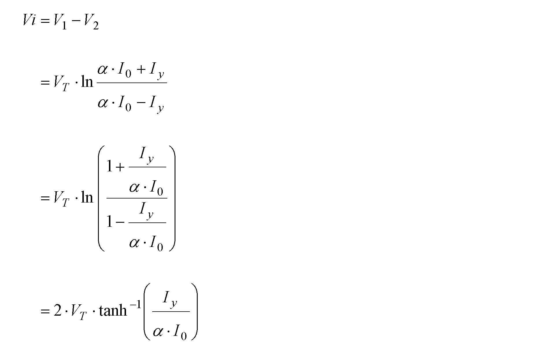
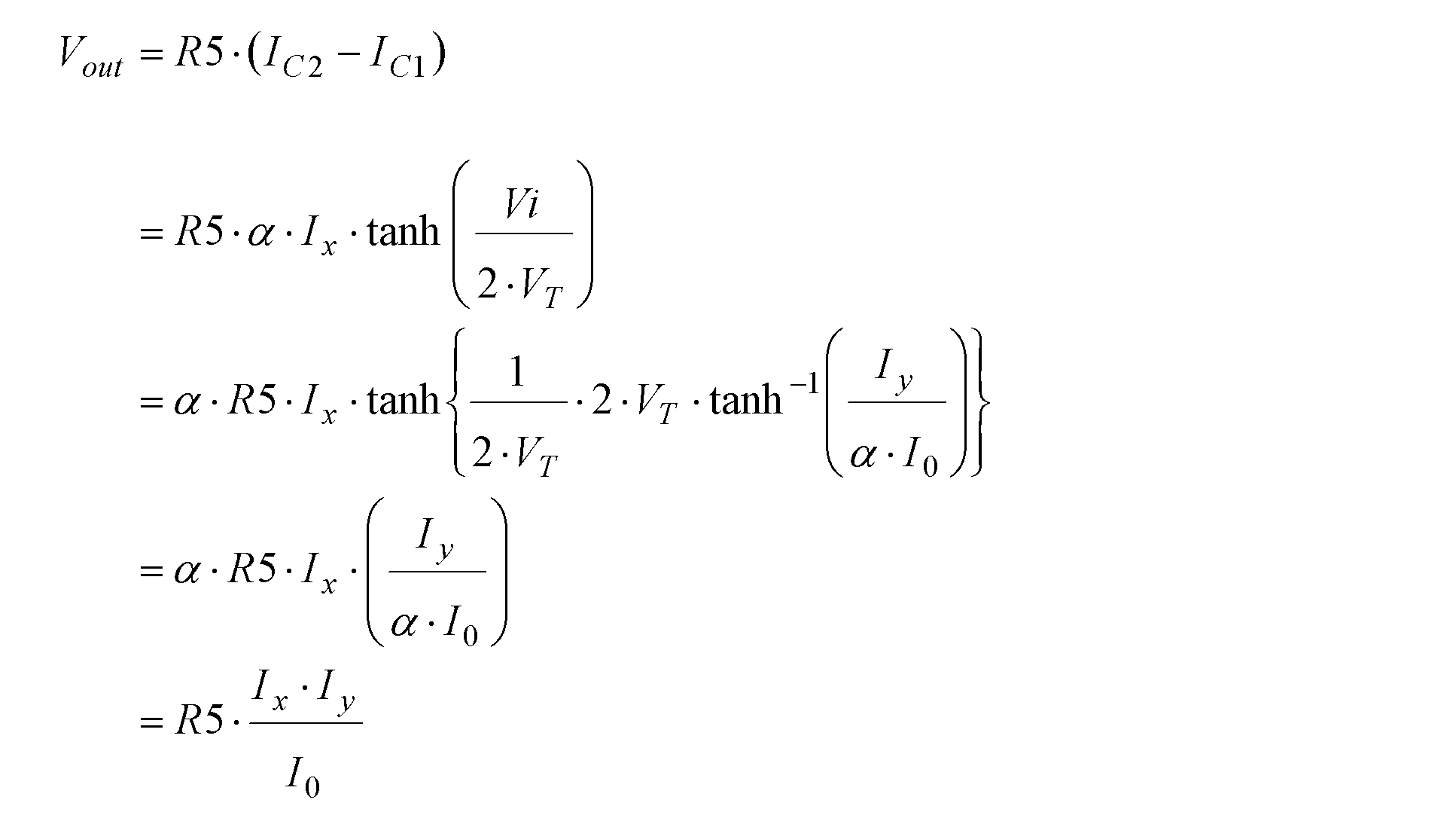
Vout=R5・K1・K2・Vx・Vy/I0
既に述べたように、本発明によるアナログ乗算回路は、補正電流生成回路により、アナログ乗算部のトランジスタの電流増幅率αに応じて増加する補正電流を生成し、当該補正電流を乗算コアの一方の入力信号に加える点に回路構成に関する特徴を有し、これにより、アナログ乗算部を構成するトランジスタの電流増幅率αが温度等で変動しても、乗算結果が当該変動の影響を受けなくなる効果が得られる。
Claims (9)
- エミッタ結合した一対のバイポーラトランジスタからなる差動トランジスタ対を少なくとも1つ有し、前記差動トランジスタ対の結合されたエミッタを第1の入力端子とし、前記差動トランジスタ対の2つのベースを第2の入力端子対とし、前記差動トランジスタ対の2つのコレクタを出力端子対とする乗算コアと、
前記第2の入力端子対にそれぞれエミッタが接続された一対のバイポーラトランジスタからなる線形化トランジスタ対を有し、前記線形化トランジスタ対の各ベース及び各コレクタをそれぞれ所定の電源に接続した線形化回路と、
前記差動トランジスタ対の各バイポーラトランジスタの電流増幅率に応じた補正電流を前記第2の入力端子対に加算する補正電流生成回路と、
を備えたことを特徴とするアナログ乗算回路。 - 前記補正電流生成回路は、前記差動トランジスタ対の各バイポーラトランジスタのレプリカである第1のレプリカトランジスタを有し、前記第1のレプリカトランジスタのエミッタへ所定のバイアス電流を流すことで前記第1のレプリカトランジスタのコレクタから得られる電流に基づいて前記補正電流を生成すること、
を特徴とする請求項1に記載のアナログ乗算回路。 - 前記補正電流生成回路は、前記線形化トランジスタ対の各バイポーラトランジスタのレプリカである第2のレプリカトランジスタを有し、
前記第2のレプリカトランジスタのエミッタを前記第1のレプリカトランジスタのベースに接続し、前記第2のレプリカトランジスタのコレクタとベースをそれぞれ所定の電源に接続したこと、
を特徴とする請求項2に記載のアナログ乗算回路。 - 前記補正電流生成回路は、
前記乗算コア及び前記線形化回路のレプリカであり、前記第1及び第2の入力端子、並びに前記出力端子それぞれのレプリカである第1及び第2のレプリカ入力端子、並びにレプリカ出力端子を有するレプリカ乗算部と、
前記レプリカ出力端子からの出力に応じた試行出力信号を期待信号と比較し比較結果信号を出力する比較回路と、
前記第1及び第2のレプリカ入力端子それぞれに所定の予備入力値に応じた信号を入力し、かつ当該入力値の積を表す所定の期待値に応じた前記期待信号を前記比較回路に入力する前記する設定回路と、
前記補正電流と当該補正電流のレプリカ電流であり前記第2のレプリカ入力端子対に加算されるレプリカ補正電流とを生成する補正電流出力回路と、
を備え、
前記補正電流出力回路は、前記試行出力信号が前記期待信号と等しくなるように前記比較結果信号に応じて前記補正電流及び前記レプリカ補正電流を増減すること、
を特徴とする請求項1に記載のアナログ乗算回路。 - 前記乗算コアは2つの前記差動トランジスタ対を有し、2つの前記差動トランジスタ対それぞれの結合されたエミッタを前記第1の入力端子対とし、2つの前記差動トランジスタ対相互間で2つのベース同士を互いに結合して前記第2の入力端子対とし、2つの前記差動トランジスタ対相互間で2つのコレクタ同士を互いに結合して前記出力端子対とすること、
を特徴とする請求項1から請求項4のいずれか一項に記載のアナログ乗算回路。 - 請求項1から請求項4のいずれか一項に記載のアナログ乗算回路を備え、
前記第1の入力端子に直流制御信号を入力し、
前記第2の入力端子に入力信号を入力し、
前記出力端子の出力信号に基づいて可変信号を得ること、
を特徴とする可変ゲインアンプ。 - 請求項5に記載のアナログ乗算回路を備え、
前記第1の入力端子又は前記第2の入力端子のいずれか一方に振幅が一定な交番信号を入力し、他方に被検波信号を入力し、
前記出力端子の出力信号に基づいて検波信号を得ること、
を特徴とする検波回路。 - 外部から印加された物理量を電気信号に変換する振動子と、参照信号を出力する参照信号生成回路と、前記参照信号に基づいて前記振動子を発振させる発振回路と、該発振回路からの発振信号に基づいて前記振動子からの出力信号を検波する検波回路と、を有する物理量センサにおいて、
前記検波回路が請求項7に記載の検波回路であって、前記交番信号が前記発振信号であり、前記被検波信号が前記振動子からの出力信号であること、
を特徴とする物理量センサ。 - 前記補正電流生成回路は、前記参照信号に基づいて前記補正電流を生成すること、
を特徴とする請求項8に記載の物理量センサ。
Priority Applications (3)
| Application Number | Priority Date | Filing Date | Title |
|---|---|---|---|
| CN201280020445.5A CN103493366B (zh) | 2011-04-25 | 2012-04-25 | 模拟乘法电路、可变增益放大器、检波电路和物理量传感器 |
| US14/114,109 US9396362B2 (en) | 2011-04-25 | 2012-04-25 | Analog multiplier circuit, variable gain amplifier, detector circuit, and physical quantity sensor |
| JP2013512402A JP5956983B2 (ja) | 2011-04-25 | 2012-04-25 | アナログ乗算回路、可変ゲインアンプ、検波回路及び物理量センサ |
Applications Claiming Priority (2)
| Application Number | Priority Date | Filing Date | Title |
|---|---|---|---|
| JP2011-097012 | 2011-04-25 | ||
| JP2011097012 | 2011-04-25 |
Publications (1)
| Publication Number | Publication Date |
|---|---|
| WO2012147784A1 true WO2012147784A1 (ja) | 2012-11-01 |
Family
ID=47072302
Family Applications (1)
| Application Number | Title | Priority Date | Filing Date |
|---|---|---|---|
| PCT/JP2012/061075 Ceased WO2012147784A1 (ja) | 2011-04-25 | 2012-04-25 | アナログ乗算回路、可変ゲインアンプ、検波回路及び物理量センサ |
Country Status (4)
| Country | Link |
|---|---|
| US (1) | US9396362B2 (ja) |
| JP (1) | JP5956983B2 (ja) |
| CN (1) | CN103493366B (ja) |
| WO (1) | WO2012147784A1 (ja) |
Families Citing this family (5)
| Publication number | Priority date | Publication date | Assignee | Title |
|---|---|---|---|---|
| JP6464526B2 (ja) * | 2015-07-01 | 2019-02-06 | パナソニックIpマネジメント株式会社 | 高周波出力制御回路 |
| US9735738B2 (en) * | 2016-01-06 | 2017-08-15 | Analog Devices Global | Low-voltage low-power variable gain amplifier |
| US11309738B2 (en) * | 2018-08-01 | 2022-04-19 | Integrated Device Technology, Inc. | Recovery of modulation amplitude in wireless charger tx demodulation |
| JP6521207B1 (ja) * | 2018-11-08 | 2019-05-29 | Tdk株式会社 | 積和演算器、積和演算方法、論理演算デバイスおよびニューロモーフィックデバイス |
| CN111751577A (zh) * | 2019-03-29 | 2020-10-09 | 中国科学院物理研究所 | 音叉型原子力显微镜探头和应用 |
Citations (4)
| Publication number | Priority date | Publication date | Assignee | Title |
|---|---|---|---|---|
| JPS6338313A (ja) * | 1986-08-02 | 1988-02-18 | Sony Corp | 増幅回路 |
| JP2005512384A (ja) * | 2001-11-28 | 2005-04-28 | ティーティーピーコム リミテッド | Rf送信機電力制御システム |
| JP2007081530A (ja) * | 2005-09-12 | 2007-03-29 | Citizen Watch Co Ltd | 増幅回路及びそれを用いた物理量センサ |
| JP2008219116A (ja) * | 2007-02-28 | 2008-09-18 | Sony Corp | ゲイン補正回路、位相同期回路及びフィルタ回路 |
Family Cites Families (14)
| Publication number | Priority date | Publication date | Assignee | Title |
|---|---|---|---|---|
| JP2603968B2 (ja) * | 1987-10-12 | 1997-04-23 | 株式会社東芝 | 線形差動増幅回路 |
| US5182477A (en) * | 1990-03-22 | 1993-01-26 | Silicon Systems, Inc. | Bipolar tunable transconductance element |
| US5712810A (en) * | 1994-06-13 | 1998-01-27 | Nec Corporation | Analog multiplier and multiplier core circuit used therefor |
| US5831468A (en) * | 1994-11-30 | 1998-11-03 | Nec Corporation | Multiplier core circuit using quadritail cell for low-voltage operation on a semiconductor integrated circuit device |
| US5668750A (en) * | 1995-07-28 | 1997-09-16 | Nec Corporation | Bipolar multiplier with wide input voltage range using multitail cell |
| US5684431A (en) * | 1995-12-13 | 1997-11-04 | Analog Devices | Differential-input single-supply variable gain amplifier having linear-in-dB gain control |
| US5912834A (en) * | 1996-04-12 | 1999-06-15 | Nec Corporation | Bipolar translinear four-quadrant analog multiplier |
| JPH1012627A (ja) | 1996-06-19 | 1998-01-16 | Nissan Motor Co Ltd | 半導体装置 |
| US6456142B1 (en) * | 2000-11-28 | 2002-09-24 | Analog Devices, Inc. | Circuit having dual feedback multipliers |
| DE10134754A1 (de) * | 2001-07-17 | 2003-02-06 | Infineon Technologies Ag | Multipliziererschaltung |
| US7310656B1 (en) * | 2002-12-02 | 2007-12-18 | Analog Devices, Inc. | Grounded emitter logarithmic circuit |
| JP4324463B2 (ja) | 2003-12-25 | 2009-09-02 | シャープ株式会社 | 検波回路装置およびそれを用いた信号検波回路システム |
| CN201007707Y (zh) * | 2006-10-31 | 2008-01-16 | 上海化工研究院 | 红外光谱仪非线性校正电路 |
| CN103140737B (zh) * | 2010-09-30 | 2015-09-16 | 西铁城控股株式会社 | 物理量传感器 |
-
2012
- 2012-04-25 JP JP2013512402A patent/JP5956983B2/ja not_active Expired - Fee Related
- 2012-04-25 WO PCT/JP2012/061075 patent/WO2012147784A1/ja not_active Ceased
- 2012-04-25 CN CN201280020445.5A patent/CN103493366B/zh not_active Expired - Fee Related
- 2012-04-25 US US14/114,109 patent/US9396362B2/en not_active Expired - Fee Related
Patent Citations (4)
| Publication number | Priority date | Publication date | Assignee | Title |
|---|---|---|---|---|
| JPS6338313A (ja) * | 1986-08-02 | 1988-02-18 | Sony Corp | 増幅回路 |
| JP2005512384A (ja) * | 2001-11-28 | 2005-04-28 | ティーティーピーコム リミテッド | Rf送信機電力制御システム |
| JP2007081530A (ja) * | 2005-09-12 | 2007-03-29 | Citizen Watch Co Ltd | 増幅回路及びそれを用いた物理量センサ |
| JP2008219116A (ja) * | 2007-02-28 | 2008-09-18 | Sony Corp | ゲイン補正回路、位相同期回路及びフィルタ回路 |
Also Published As
| Publication number | Publication date |
|---|---|
| JP5956983B2 (ja) | 2016-07-27 |
| CN103493366B (zh) | 2016-08-24 |
| US20140047920A1 (en) | 2014-02-20 |
| US9396362B2 (en) | 2016-07-19 |
| JPWO2012147784A1 (ja) | 2014-07-28 |
| CN103493366A (zh) | 2014-01-01 |
Similar Documents
| Publication | Publication Date | Title |
|---|---|---|
| CN106716149B (zh) | 霍尔电动势信号检测电路以及电流传感器 | |
| JP5774016B2 (ja) | 物理量センサ | |
| CN205195662U (zh) | 共模反馈电路和信号处理电路 | |
| CN102323847B (zh) | 基于温度补偿的电压基准电路 | |
| JP5956983B2 (ja) | アナログ乗算回路、可変ゲインアンプ、検波回路及び物理量センサ | |
| US8240204B2 (en) | Synchronous detection circuit, sensing circuit, physical quantity measuring device, gyro sensor, and electronic apparatus | |
| CN102393785B (zh) | 一种低失调带隙基准电压源 | |
| US7750743B2 (en) | Compensating quantity-providing circuit, stress-compensating circuit, stress-compensated circuit, apparatus for providing a compensating quantity, method for providing a compensating quantity and ring oscillator | |
| CN104949767A (zh) | 温度测量装置、集成电路及温度测量方法 | |
| JP2006086857A (ja) | 移相装置 | |
| JPH10303664A (ja) | 可変利得増幅器 | |
| JP2008017354A (ja) | オフセット電圧補正回路 | |
| JP6099465B2 (ja) | アクティブバラン | |
| US8922279B2 (en) | Voltage controlled variable gain amplifier circuit | |
| JP3578136B2 (ja) | 掛け算器 | |
| CN103095306B (zh) | 对数/反对数转换电路 | |
| JP3442613B2 (ja) | 可変利得増幅器 | |
| Revanna et al. | Low frequency CMOS sinusoidal oscillator for impedance spectroscopy | |
| JP6000884B2 (ja) | 演算増幅回路 | |
| JP2004064262A (ja) | 差動増幅回路及び電波時計用受信回路 | |
| JP2012211809A (ja) | 物理量センサ | |
| Brkic et al. | One solution for CMOS precision rectifier | |
| JP5658074B2 (ja) | トランスリニア回路 | |
| CN120177864A (zh) | 一种功率检测器及微波雷达 | |
| JP2009152859A (ja) | 半導体集積回路 |
Legal Events
| Date | Code | Title | Description |
|---|---|---|---|
| 121 | Ep: the epo has been informed by wipo that ep was designated in this application |
Ref document number: 12777142 Country of ref document: EP Kind code of ref document: A1 |
|
| ENP | Entry into the national phase |
Ref document number: 2013512402 Country of ref document: JP Kind code of ref document: A |
|
| NENP | Non-entry into the national phase |
Ref country code: DE |
|
| WWE | Wipo information: entry into national phase |
Ref document number: 14114109 Country of ref document: US |
|
| 122 | Ep: pct application non-entry in european phase |
Ref document number: 12777142 Country of ref document: EP Kind code of ref document: A1 |