WO2012147456A1 - 半導体装置 - Google Patents
半導体装置 Download PDFInfo
- Publication number
- WO2012147456A1 WO2012147456A1 PCT/JP2012/058858 JP2012058858W WO2012147456A1 WO 2012147456 A1 WO2012147456 A1 WO 2012147456A1 JP 2012058858 W JP2012058858 W JP 2012058858W WO 2012147456 A1 WO2012147456 A1 WO 2012147456A1
- Authority
- WO
- WIPO (PCT)
- Prior art keywords
- region
- gate electrode
- mosfet
- drain
- semiconductor device
- Prior art date
- Legal status (The legal status is an assumption and is not a legal conclusion. Google has not performed a legal analysis and makes no representation as to the accuracy of the status listed.)
- Ceased
Links
Images







Classifications
-
- H—ELECTRICITY
- H10—SEMICONDUCTOR DEVICES; ELECTRIC SOLID-STATE DEVICES NOT OTHERWISE PROVIDED FOR
- H10D—INORGANIC ELECTRIC SEMICONDUCTOR DEVICES
- H10D84/00—Integrated devices formed in or on semiconductor substrates that comprise only semiconducting layers, e.g. on Si wafers or on GaAs-on-Si wafers
- H10D84/80—Integrated devices formed in or on semiconductor substrates that comprise only semiconducting layers, e.g. on Si wafers or on GaAs-on-Si wafers characterised by the integration of at least one component covered by groups H10D12/00 or H10D30/00, e.g. integration of IGFETs
- H10D84/811—Combinations of field-effect devices and one or more diodes, capacitors or resistors
- H10D84/817—Combinations of field-effect devices and resistors only
-
- H—ELECTRICITY
- H10—SEMICONDUCTOR DEVICES; ELECTRIC SOLID-STATE DEVICES NOT OTHERWISE PROVIDED FOR
- H10D—INORGANIC ELECTRIC SEMICONDUCTOR DEVICES
- H10D30/00—Field-effect transistors [FET]
- H10D30/01—Manufacture or treatment
- H10D30/021—Manufacture or treatment of FETs having insulated gates [IGFET]
- H10D30/0212—Manufacture or treatment of FETs having insulated gates [IGFET] using self-aligned silicidation
-
- H—ELECTRICITY
- H10—SEMICONDUCTOR DEVICES; ELECTRIC SOLID-STATE DEVICES NOT OTHERWISE PROVIDED FOR
- H10D—INORGANIC ELECTRIC SEMICONDUCTOR DEVICES
- H10D30/00—Field-effect transistors [FET]
- H10D30/60—Insulated-gate field-effect transistors [IGFET]
- H10D30/601—Insulated-gate field-effect transistors [IGFET] having lightly-doped drain or source extensions, e.g. LDD IGFETs or DDD IGFETs
- H10D30/603—Insulated-gate field-effect transistors [IGFET] having lightly-doped drain or source extensions, e.g. LDD IGFETs or DDD IGFETs having asymmetry in the channel direction, e.g. lateral high-voltage MISFETs having drain offset region or extended drain IGFETs [EDMOS]
-
- H—ELECTRICITY
- H10—SEMICONDUCTOR DEVICES; ELECTRIC SOLID-STATE DEVICES NOT OTHERWISE PROVIDED FOR
- H10D—INORGANIC ELECTRIC SEMICONDUCTOR DEVICES
- H10D30/00—Field-effect transistors [FET]
- H10D30/60—Insulated-gate field-effect transistors [IGFET]
- H10D30/601—Insulated-gate field-effect transistors [IGFET] having lightly-doped drain or source extensions, e.g. LDD IGFETs or DDD IGFETs
- H10D30/605—Insulated-gate field-effect transistors [IGFET] having lightly-doped drain or source extensions, e.g. LDD IGFETs or DDD IGFETs having significant overlap between the lightly-doped extensions and the gate electrode
-
- H—ELECTRICITY
- H10—SEMICONDUCTOR DEVICES; ELECTRIC SOLID-STATE DEVICES NOT OTHERWISE PROVIDED FOR
- H10D—INORGANIC ELECTRIC SEMICONDUCTOR DEVICES
- H10D89/00—Aspects of integrated devices not covered by groups H10D84/00 - H10D88/00
- H10D89/60—Integrated devices comprising arrangements for electrical or thermal protection, e.g. protection circuits against electrostatic discharge [ESD]
- H10D89/601—Integrated devices comprising arrangements for electrical or thermal protection, e.g. protection circuits against electrostatic discharge [ESD] for devices having insulated gate electrodes, e.g. for IGFETs or IGBTs
- H10D89/811—Integrated devices comprising arrangements for electrical or thermal protection, e.g. protection circuits against electrostatic discharge [ESD] for devices having insulated gate electrodes, e.g. for IGFETs or IGBTs using FETs as protective elements
-
- H—ELECTRICITY
- H10—SEMICONDUCTOR DEVICES; ELECTRIC SOLID-STATE DEVICES NOT OTHERWISE PROVIDED FOR
- H10D—INORGANIC ELECTRIC SEMICONDUCTOR DEVICES
- H10D84/00—Integrated devices formed in or on semiconductor substrates that comprise only semiconducting layers, e.g. on Si wafers or on GaAs-on-Si wafers
- H10D84/01—Manufacture or treatment
- H10D84/0123—Integrating together multiple components covered by H10D12/00 or H10D30/00, e.g. integrating multiple IGBTs
- H10D84/0126—Integrating together multiple components covered by H10D12/00 or H10D30/00, e.g. integrating multiple IGBTs the components including insulated gates, e.g. IGFETs
- H10D84/013—Manufacturing their source or drain regions, e.g. silicided source or drain regions
-
- H—ELECTRICITY
- H10—SEMICONDUCTOR DEVICES; ELECTRIC SOLID-STATE DEVICES NOT OTHERWISE PROVIDED FOR
- H10D—INORGANIC ELECTRIC SEMICONDUCTOR DEVICES
- H10D84/00—Integrated devices formed in or on semiconductor substrates that comprise only semiconducting layers, e.g. on Si wafers or on GaAs-on-Si wafers
- H10D84/01—Manufacture or treatment
- H10D84/0123—Integrating together multiple components covered by H10D12/00 or H10D30/00, e.g. integrating multiple IGBTs
- H10D84/0126—Integrating together multiple components covered by H10D12/00 or H10D30/00, e.g. integrating multiple IGBTs the components including insulated gates, e.g. IGFETs
- H10D84/0135—Manufacturing their gate conductors
- H10D84/0142—Manufacturing their gate conductors the gate conductors having different shapes or dimensions
-
- H—ELECTRICITY
- H10—SEMICONDUCTOR DEVICES; ELECTRIC SOLID-STATE DEVICES NOT OTHERWISE PROVIDED FOR
- H10D—INORGANIC ELECTRIC SEMICONDUCTOR DEVICES
- H10D84/00—Integrated devices formed in or on semiconductor substrates that comprise only semiconducting layers, e.g. on Si wafers or on GaAs-on-Si wafers
- H10D84/01—Manufacture or treatment
- H10D84/0123—Integrating together multiple components covered by H10D12/00 or H10D30/00, e.g. integrating multiple IGBTs
- H10D84/0126—Integrating together multiple components covered by H10D12/00 or H10D30/00, e.g. integrating multiple IGBTs the components including insulated gates, e.g. IGFETs
- H10D84/0144—Manufacturing their gate insulating layers
-
- H—ELECTRICITY
- H10—SEMICONDUCTOR DEVICES; ELECTRIC SOLID-STATE DEVICES NOT OTHERWISE PROVIDED FOR
- H10D—INORGANIC ELECTRIC SEMICONDUCTOR DEVICES
- H10D84/00—Integrated devices formed in or on semiconductor substrates that comprise only semiconducting layers, e.g. on Si wafers or on GaAs-on-Si wafers
- H10D84/01—Manufacture or treatment
- H10D84/02—Manufacture or treatment characterised by using material-based technologies
- H10D84/03—Manufacture or treatment characterised by using material-based technologies using Group IV technology, e.g. silicon technology or silicon-carbide [SiC] technology
- H10D84/038—Manufacture or treatment characterised by using material-based technologies using Group IV technology, e.g. silicon technology or silicon-carbide [SiC] technology using silicon technology, e.g. SiGe
Definitions
- the present invention relates to a semiconductor device, and more particularly, to an SGGMOS (Source-Gate-GND-Metal-Oxide-Semiconductor-Transistor) type ESD (Electro-Static Discharge) protection element for preventing a current such as an electrostatic surge from flowing into a semiconductor integrated circuit device. .
- SGGMOS Source-Gate-GND-Metal-Oxide-Semiconductor-Transistor
- ESD Electro-Static Discharge
- a semiconductor integrated circuit IC includes an ESD protection element for protecting the semiconductor integrated circuit from external noise such as electrostatic surge.
- the so-called “off transistor”, which is used by grounding the source and gate of a transistor, can clamp a surge current at a lower voltage than when a diode is used by snapback operation. Widely adopted.
- Patent Document 1 a non-silicide region where no silicide is formed is provided in a region adjacent to the electrode portion of the drain region, and a resistance due to a diffusion layer is formed in the non-silicide region.
- a silicide block forming step it is necessary to add a silicide block forming step in order to form the non-silicide region.
- an object of the present invention is to realize a semiconductor device capable of improving the ESD discharge capability without increasing the number of special processes and dedicated masks for ESD countermeasures.
- a semiconductor device provides: A first region where a first MOSFET is formed; A first ESD protection element formed by connecting a first protection resistance circuit to the first MOSFET is formed on the first region,
- the first MOSFET is: A first gate electrode formed on the first well via a first gate insulating film; and A first source region and a first drain region having a conductivity type opposite to that of the first well formed on a surface layer of the first well so as to face each other with the first gate electrode interposed therebetween;
- the first protective resistance circuit includes: A first gate electrode formed through the first gate insulating film; Two first resistance drain regions having a conductivity type opposite to that of the first well formed to be separated from each other in a surface layer of the first well so as to face each other with the first gate electrode interposed therebetween; A drift region having the same conductivity type as the first resistance drain region and having a lower concentration than the first resistance drain region;
- a first feature is that the drift region is formed below the first gate electrode so as to be electrical
- the first MOSFET further includes:
- the first MOSFET has the same conductivity type as the first source region and the first drain region, and includes a drift region having a lower concentration than the first source region and the first drain region,
- the drift region of the first MOSFET extends from the first source region of the first MOSFET toward the lower side of the first gate electrode, and the first drain of the first MOSFET.
- a drain-side drift region extending downward from the region toward the lower side of the first gate electrode is separated and formed across the first well below the first gate electrode of the first MOSFET, It is preferable that the drain side drift region of the first MOSFET constituting the first ESD protection element is connected to the drift region of the first protection resistance circuit.
- the first gate electrode of the first MOSFET and the first gate electrode of the first protective resistance circuit are made of polysilicon. preferable.
- the semiconductor device of the first feature further includes a silicide layer formed on an upper surface of the first gate electrode of the first protective resistance circuit, and a silicide layer formed on an upper surface of the first resistance drain region.
- the first protective resistance circuit may be electrically isolated through an insulating film formed along a side wall of the first gate electrode.
- the semiconductor device further includes a second region in which a second MOSFET having a lower withstand voltage than the first MOSFET is formed, A second ESD protection element formed by connecting a second protection resistance circuit to the second MOSFET is formed on the second region,
- the second MOSFET is: A second gate electrode formed on the second well via a second gate insulating film; and A second source region and a second drain region having a conductivity type opposite to that of the second well formed on a surface layer of the second well so as to face each other with the second gate electrode interposed therebetween;
- the second protective resistance circuit is: A second gate electrode formed through the second gate insulating film; Two second resistance drain regions having a conductivity type opposite to that of the second well formed to be separated from each other in a surface layer of the second well so as to face each other across the second gate electrode; and A second drift region having the same conductivity type as the second resistance drain region and having a lower concentration than the second resistance drain region;
- the second feature is that the second drift region is formed below the second
- the second gate electrode is made of polysilicon
- the silicide layer formed on the upper surface of the second gate electrode of the second protection resistance circuit includes the silicide layer formed on the upper surface of the second resistance drain region, and the second layer of the second protection resistance circuit.
- a structure in which the gate electrode is electrically isolated through an insulating film formed along the side wall of the gate electrode can be employed.
- the semiconductor device according to the second feature is further characterized in that, in the second MOSFET, the semiconductor device is electrically connected to either the second source region or the second drain region, and extends downward from the second gate electrode.
- an LDD region having the same conductivity type as the second source region and the second drain region and having a lower concentration than the second source region and the second drain region is preferably formed.
- the semiconductor device is further configured to be electrically connected to any one of the first source region and the first drain region in the first MOSFET and extend downward from the first gate electrode.
- an LDD region having the same conductivity type as the first source region and the first drain region and having a lower concentration than the first source region and the first drain region is preferably formed.
- a dummy gate pattern is formed in a region where the protective resistance circuit is formed, and a resistance drift region is formed immediately below the dummy gate pattern. Has been. Therefore, the protective resistance circuit has a dummy gate electrode on the drift region.
- the ESD element according to the present invention is configured by connecting a MOSFET and the protection resistance circuit in series, and the protection resistance circuit forms a drift region that connects a resistance drain region (corresponding to a source region and a drain region). Except for this, it has the same structure as the MOSFET.
- the dummy gate electrode of the protective resistance circuit and the insulating film formed on the sidewall of the dummy gate electrode function as a silicide block. That's what it meant.
- the formation of the dummy gate pattern for forming the dummy gate electrode of the protective resistance circuit is the same as the formation of the MOSFET gate pattern, and the formation of the drift region for resistance is the same as the formation of the drift region of the high voltage MOSFET. Therefore, the ESD protection element can be formed without increasing the number of manufacturing steps.
- the present invention can be applied to an integrated circuit including both a high breakdown voltage MOSFET and a low breakdown voltage MOSFET, thereby increasing the number of manufacturing steps. Therefore, it is possible to form both the high withstand voltage ESD element and the low withstand voltage ESD element.
- the low breakdown voltage MOSFET may be a MOSFET having an LDD region. In this case, the LDD region is also formed in the protective resistance circuit in the low breakdown voltage ESD element, but the operation as a resistance circuit is not affected.
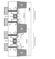
- 1 is a cross-sectional view schematically showing the structure of a semiconductor device according to an embodiment of the present invention.
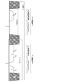
- 1 is a cross-sectional view schematically showing the structure of a semiconductor device according to an embodiment of the present invention.
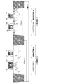
- Process sectional drawing which shows typically the manufacturing method of the semiconductor device which concerns on one Embodiment of this invention.
- Process sectional drawing which shows typically the manufacturing method of the semiconductor device which concerns on one Embodiment of this invention.
- Process sectional drawing which shows typically the manufacturing method of the semiconductor device which concerns on one Embodiment of this invention.
- Process sectional drawing which shows typically the manufacturing method of the semiconductor device which concerns on one Embodiment of this invention.
- Process sectional drawing which shows typically the manufacturing method of the semiconductor device which concerns on one Embodiment of this invention.
- Process sectional drawing which shows typically the manufacturing method of the semiconductor device which concerns on one Embodiment of this invention.
- Process sectional drawing which shows typically the manufacturing method of the semiconductor device which concerns on one Embodiment of this invention.
- Process sectional drawing which shows typically the manufacturing method of the semiconductor device which concerns on one Embodiment of this invention.
- FIGS. 1 and 2 are cross-sectional views schematically showing the device structure of the device 1 of the present invention. Note that, in the cross-sectional views shown in FIGS. 1 and 2, the main parts are appropriately emphasized, and the dimensional ratios of the respective components on the drawings do not necessarily match the actual dimensional ratios. The same applies to the cross-sectional views shown below.
- the device 100 of the present invention includes a first region in which a first MOSFET (high-voltage MOSFET: hereinafter referred to as “HV transistor” as appropriate) that operates in response to a first power supply voltage is formed,
- the first region has a second region in which a second MOSFET (low-voltage MOSFET: hereinafter referred to as “LV transistor” as appropriate) that operates in response to a second power source voltage lower than the power source voltage is formed.
- a first ESD protection element (HV protection element) for high withstand voltage formed by connecting a first protection resistance circuit to the first MOSFET is provided with a second protection for the second MOSFET on the second region.
- a low withstand voltage second ESD protection element (LV protection element) is formed by connecting a resistance circuit.
- FIG. 1 is a cross-sectional view of the device structure of an ESD protection element (HV protection element and LV protection element) provided in the device 100 of the present invention
- FIG. 2 shows a MOSFET (HV transistor, Cross-sectional views of device structures of LV transistors) are shown.
- HV protection element and LV protection element HV protection element and LV protection element
- MOSFET HV transistor, Cross-sectional views of device structures of LV transistors
- P-type wells 2 and 3 are formed on a P-type substrate 1
- an HV protection element 21 is formed on the well 2
- an LV protection element 22 is formed on the well 3.
- the HV protection element 21 and the LV protection element 22 are separated by an element isolation film (STI) 4.
- STI element isolation film
- P-type wells 2 and 3 are formed on a P-type substrate 1
- an HV transistor 23 is formed on the well 2
- an LV transistor 24 is formed on the well 3.
- the HV transistor 23 and the LV transistor 24 are separated by an element isolation film (STI) 4.
- STI element isolation film
- the HV transistor 23 is opposed to each other with the gate electrode (first gate electrode) 8a formed on the well 2 via the gate insulating film (first gate insulating film) 6 and the gate electrode 8a interposed therebetween.
- the N-channel MOSFET is provided with an N + type high concentration source region (first source region) 11a and an N + type high concentration drain region (first drain region) 11b formed in the surface layer of the well 2.
- an N ⁇ type drift region 5 (5a, 5b) is formed at a deeper position than the high concentration source / drain regions 11a, 11b so as to cover the high concentration source region 11a and the high concentration drain region 11b.
- the drift regions 5a and 5b are formed so as to extend downward from the gate electrode 8a, respectively, but are separately formed via the P-type well 2 existing below the gate electrode 8a.
- a sidewall insulating film 10a is formed along the sidewall of the gate electrode 8a.
- the sidewall insulating film 10a is made of, for example, a silicon oxide film or a nitride film.
- the LV transistor 24 is opposed to each other with a gate electrode (second gate electrode) 8c formed on the well 3 via a gate insulating film (second gate insulating film) 7 and the gate electrode 8c interposed therebetween.
- the N-channel MOSFET is provided with an N + type high concentration source region (second source region) 11c and an N + type high concentration drain region (second drain region) 11d formed in the surface layer of the well 3.
- an N ⁇ type LDD (Lightly Doped Drain) region 9 is electrically connected to either the high concentration source region 11c or the high concentration drain region 11d and extends toward the gate electrode 8c.
- a sidewall insulating film 10c is formed along the sidewall of the gate electrode 8c.
- the sidewall insulating film 10c is made of, for example, a silicon oxide film or a nitride film.
- Contact plugs 14 penetrating the interlayer insulating film 13 are formed on the upper surfaces of the high concentration source region 11a and the high concentration drain region 11b of the HV transistor 23 and on the upper surface of the high concentration source region 11c and the high concentration drain region 11d of the LV transistor 24.
- a silicide layer 12 is formed for reducing the contact resistance with the metal wiring 15 and facilitating electrical connection with the metal wiring 15.
- the silicide layer 12 is also formed on the upper surfaces of the gate electrodes 8a and 8c made of polysilicon.
- the silicide layer formed on the upper surface of the gate electrode 8a and the silicide layers formed on the upper surfaces of the respective high concentration source regions and high concentration drain regions 11a and 11b are electrically connected by the sidewall insulating film 10a and the interlayer insulating film 13.
- the silicide layer formed on the upper surface of the gate electrode 8c and the silicide layer formed on the upper surfaces of the high-concentration source regions and the high-concentration drain regions 11c and 11d are separated by the sidewall insulating film 10c and the interlayer insulating film 13. Electrically separated.
- the HV protection element 21 connects the protection resistance circuit 25 to the high concentration drain region 11 b of the HV transistor 23, and the LV protection element 22 connects the protection resistance circuit 25 to the high concentration drain region 11 d of the LV transistor 24. Configured.
- the protective resistance circuit 25 includes both the N + type drain region (first resistance drain region) 16 formed so that the drift region 5 (5c) is opposed to the surface layer of the well 2 with the gate electrode 8b interposed therebetween. It has the same structure as the HV transistor 23 except that it is formed so as to be electrically connected.
- each of the two drain regions 16 formed separately corresponds to the high-concentration source region 11a and the high-concentration drain region 11b in the HV transistor 23.
- the drift region 5c is integrally formed so as to overlap the drift region 5b of the adjacent HV transistor 23.
- One of the drain regions 16 of the protective resistance circuit 25 is connected to the high-concentration drain region 11b of the HV transistor 23, and the other drain region 16 of the protective resistance circuit 25 is connected to the metal wiring 15 through the contact plug 14.
- the protective resistance circuit 25 is configured such that the two drain regions 16 that are separately formed are electrically connected to each other by the same conductivity type (N-type) drift region 5c, so that there is no P-type channel region. It does not operate as a transistor and operates as a resistor.
- the gate electrode 8b is formed as a dummy electrode for blocking the formation of silicide, and no voltage is actually applied thereto. It is possible to change the resistance value of the protective resistance circuit 25 by adjusting the width L between the source and drain of the gate electrode 8b.
- the protective resistance circuit 26 has the same structure as the LV transistor 24.
- each of the N + type drain regions (second resistance drain regions) 17 separately formed so as to face each other on the surface layer of the well 3 with the gate electrode 8d interposed therebetween is the high concentration source region 11c in the LV transistor 24. This corresponds to the high concentration drain region 11d.
- an N ⁇ type drift region (second drift region) 5 d that is electrically connected to both the drain region 17 is formed below the gate electrode 8 d and deeper than the drain region 17.
- One of the drain regions 17 of the protective resistance circuit 26 is connected to the high concentration drain region 11 d of the LV transistor 24, and the other drain region 17 of the protective resistance circuit 26 is connected to the metal wiring 15 through the contact plug 14.
- the protective resistance circuit 26 operates as a resistance by electrically connecting the two drain regions 17 that are separately formed by the drift region 5d of the same conductivity type.
- the gate electrode 8d is formed as a dummy electrode for blocking the formation of silicide, and no voltage is actually applied.
- the resistance value of the protective resistance circuit 26 can be changed by adjusting the width L between the source and drain of the gate electrode 8d.
- silicide layers 12 are formed on the upper surfaces of the gate electrodes 8b and 8d made of polysilicon and the upper surfaces of the drain regions 16 and 17, respectively.
- the silicide layer formed on the upper surface of the gate electrode 8b is electrically separated by the silicide layer formed on each upper surface of the drain region 16, the sidewall insulating film 10b, and the interlayer insulating film 13, and the gate electrode 8d
- the silicide layer formed on the upper surface is electrically separated by the silicide layer formed on each upper surface of the drain region 17, the sidewall insulating film 10 d and the interlayer insulating film 13. For this reason, the current flows between the separated drain regions 16 via the drift region 5c, or flows between the separated drain regions 17 via the drift region 5d, so that the drift regions 5c and 5d are resistant to each other. Function as.
- an N ⁇ type LDD region is formed in the drift region 5d, but this does not affect the operation as a resistance circuit. .
- FIGS. 3 to 10 are process cross-sectional views schematically showing an embodiment of a method for manufacturing an ESD protection element (HV protection element 21 and LV protection element 22) of the device 1 of the present invention, corresponding to FIG. It is.
- the manufacturing method of the individual transistors (HV transistor 23 and LV transistor 24) formed in the first and second regions is formed in the HV protection element 21 of FIG.
- the manufacturing method is the same as that of the HV transistor 23 and the LV transistor 24 formed in the LV protection element 22 of FIG. 1, and is shown as a part of the steps shown in FIGS. Omit.
- a P-type well (first well) 2 is formed in a first region where an HV transistor 23 and a protective resistance circuit 25 are formed on a P-type substrate 1 by a known semiconductor process technique.
- a P-type well (second well) 3 is formed in the second region where the LV transistor 24 and the protective resistance circuit 26 are formed.
- an element isolation film (STI) 4 is formed in a predetermined region in the wells 2 and 3.
- a sacrificial oxide film is formed on the upper surfaces of the wells 2 and 3.
- an N-type impurity for example, arsenic (As) or phosphorus (P)
- a resist pattern 32 having an opening in a predetermined region by a known semiconductor process technique.
- Ion implantation is performed to form N ⁇ type low-concentration drift regions 5a and 5b in the formation region of the HV transistor 23 in the first region and drift regions 5c in the formation region of the protective resistance circuit 25 in the well 2, respectively.
- an N ⁇ type low concentration drift region 5 d is also formed in the well 3 in the formation region of the protective resistance circuit 26 on the second region.
- the first gate insulating film 6 is formed on the first region and the second gate insulating film 7 is formed on the second region by a known semiconductor process technique. Formed by oxidation.
- the first gate insulating film 6 is thicker than the second gate insulating film 7.
- a resist pattern 33 having an opening in a predetermined region is used to expose the polysilicon exposed in the opening. Silicon is removed and a gate pattern is formed. Thereby, the gate electrodes 8a to 8d are separately formed.
- the resist pattern 34 and the gate electrodes 8b and 8d on the second region are masked.
- the N ⁇ type LDD region 9 is formed in the formation region of the LV transistor 23 in the second region by ion implantation of an N type impurity (for example, phosphorus (P) or arsenic (As)).
- an N type impurity for example, phosphorus (P) or arsenic (As)
- the LDD region is also formed in the formation region of the protective resistance circuit 26 in the second region.
- an insulating film 10 (here, a silicon nitride film) is deposited on the entire surface by a known semiconductor process technique, and the gate insulating film 6, The insulating film 10 is removed until 7 is exposed. Further, the gate oxide film 6 is removed until the N ⁇ type drift regions 5a to 5d in the surface layer of the well 2 are exposed, and the gate oxide film 7 is removed until the N ⁇ type LDD region 9 in the surface layer of the well 3 is exposed. Thereby, the sidewall insulating films 10a to 10d are left on both side walls of the gate electrodes 8a to 8d.
- N-type impurities for example, phosphorus (P) or arsenic (As) are formed by a known semiconductor process technique using the gate electrodes 8a to 8d and the sidewall insulating films 10a to 10d as a mask.
- N + type high concentration first source region 11a and first drain region 11b are formed in the formation region of HV transistor 23 on the first region, and N + type high concentration second source region 11c.
- the second drain region 11d is formed in the formation region of the LV transistor 24 on the second region.
- drain regions 16 and 17 are also formed in the formation region of the protective resistance circuit 25 on the first region and the formation region of the protective resistance circuit 26 on the second region, respectively.
- metal titanium (Ti) is reacted on the surfaces of the source and drain regions 11a to 11d and the drain regions 16 and 17 of the protection resistance circuits by a known semiconductor process technique.
- the silicide layer 12 is formed.
- the silicide layer 12 is also formed on the upper surfaces of the gate electrodes 8a to 8d.
- the unreacted titanium on the sidewall insulating film 10 and the element isolation film (STI) 4 is selectively removed by wet processing.
- a contact plug 14 that penetrates the interlayer insulating film 13 and a metal wiring 15 on the contact plug 14 are formed by a known semiconductor process technique.
- the inventive device 100 shown is manufactured.
- the difference between the HV transistor 23 and the protection resistance circuit 25 in the HV protection element 21 and the difference between the LV transistor 24 and the protection resistance circuit 26 in the LV protection element 22 are as follows.
- the drain regions 16 of the protective resistance circuit corresponding to the source region 11a and the drain region 11b in FIG. 5 are connected through the drift region 5c of the same conductivity type, and the source region 11c and the drain region 11d in the LV transistor 24 It can be seen that the drain regions 17 of the protection resistance circuit corresponding to the above are connected via the drift region 5d of the same conductivity type, and it is not necessary to add any manufacturing process in forming the protection element. Therefore, the device 100 of the present invention has a structure capable of improving the ESD discharge capability without increasing the number of special processes and dedicated masks for ESD countermeasures.
- the present invention has been described by taking the ESD protection element having the SGGNMOS structure as an example.
- the SGGPMOS structure even in the case of the SGGPMOS structure, it can be easily realized by reversing the conductivity type of the impurities constituting each semiconductor region. Needless to say.
- the protective resistance circuits 25 and 26 in the SGGPMOS structure are configured by including a P ⁇ type drift region in the P channel MOSFET constituting the HV transistor 23 or the LV transistor 24.
- the present invention relates to the structure of the ESD protection element, the size (depth and area) of each semiconductor region, the impurity concentration, and the material constituting the element are not limited at all.
- a material for the gate electrodes 8a to 8d refractory metal can be used in addition to polysilicon.
- the gate insulating films 6 and 7 a high-k material may be used in addition to the thermal oxide film and the CVD oxide film, and the metal constituting the silicide may be any of cobalt, nickel, etc. in addition to titanium.
- the effect of the present invention can be obtained.
- the said embodiment has the 1st area
- the ESD protection element of the present invention is provided even when the device includes only the first region in which the high voltage transistor is formed or only the second region in which the low voltage transistor is formed. It can be set as the structure provided.
- the present invention can be used for a semiconductor device, and in particular, can be used for a semiconductor integrated circuit device including an ESD protection element.
Landscapes
- Semiconductor Integrated Circuits (AREA)
- Metal-Oxide And Bipolar Metal-Oxide Semiconductor Integrated Circuits (AREA)
Abstract
ESD対策のための特別な工程や専用マスクを増やすことなく、ESD放電能力の向上を図る事が可能な半導体装置を実現する。基板上の所定の領域に、MOSFET構造のHVトランジスタ23と保護抵抗回路25からなる高耐圧用のESD保護素子21、及び、MOSFET構造のLVトランジスタ24と保護抵抗回路26からなる低耐圧用のESD保護素子22が形成されている。当該保護抵抗回路25(26)は、ゲート電極8b(8d)を挟んで互いに対抗するようにウェル2(3)の表層に分離形成される抵抗ドリフト領域16(17)の双方が、同導電型の低濃度ドリフト領域5c(5d)により電気的に接続されていることを除き、HVトランジスタ23(LVトランジスタ24)と同一の構造である。
Description
本発明は、半導体装置に関し、特に、半導体集積回路装置に静電サージなどの電流が流れ込むのを防ぐためのSGGMOS(Source Gate GND Metal Oxide Semiconductor Transistor)型のESD(Electro-Static Discharge)保護素子に関する。
一般に、半導体集積回路ICは、静電サージなどの外部ノイズから半導体集積回路を保護するためのESD保護素子を備えている。
なかでも、SGGMOS型のESD保護素子として、トランジスタのソースとゲートを接地して使用する、所謂「オフトランジスタ」は、スナップバック動作により、ダイオードを用いる場合よりも低電圧にサージ電流をクランプできることから、広く採用されている。
当該オフトランジスタ型の保護素子では、サージ電流が入ってくるドレイン領域に保護抵抗を配置し、保護素子自体の破壊を防ぐ措置がとられている。
具体的には、特許文献1に示されているように、ドレイン領域の電極部と隣接する領域にシリサイドが形成されない非シリサイド領域を設け、当該非シリサイド領域において拡散層による抵抗を形成する。ただし、当該非シリサイド領域を形成するために、シリサイドブロック形成工程を追加する必要が生じる。
上述の通り、特許文献1に示すESD保護素子では、非シリサイド領域を形成するために、シリサイドブロックの形成工程を追加する必要があり、製造工程が複雑になるとともに、必要となるマスク数が増え、製造コスト高となる。
上述の状況を鑑み、本発明は、ESD対策のための特別な工程や専用マスクを増やすことなく、ESD放電能力の向上を図る事が可能な半導体装置を実現することをその目的とする。
上記目的を達成するための本発明に係る半導体装置は、
第1のMOSFETが形成される第1領域を有し、
前記第1領域上に、前記第1のMOSFETに第1の保護抵抗回路を接続してなる第1ESD保護素子が形成され、
前記第1のMOSFETは、
第1ウェル上に、第1ゲート絶縁膜を介して形成された第1ゲート電極、及び、
前記第1ゲート電極を挟んで互いに対向するように前記第1ウェルの表層に形成される前記第1ウェルと逆導電型の第1ソース領域及び第1ドレイン領域を備え、
前記第1の保護抵抗回路は、
前記第1ゲート絶縁膜を介して形成された第1ゲート電極、
前記第1ゲート電極を挟んで互いに対向するように前記第1ウェルの表層に分離形成される前記第1ウェルと逆導電型の二つの第1抵抗ドレイン領域、及び、
前記第1抵抗ドレイン領域と同導電型であって当該第1抵抗ドレイン領域より低濃度のドリフト領域を備え、
前記ドリフト領域が、前記第1抵抗ドレイン領域の双方と電気的に接続するように、前記第1ゲート電極下方に形成されていることを第1の特徴とする。
第1のMOSFETが形成される第1領域を有し、
前記第1領域上に、前記第1のMOSFETに第1の保護抵抗回路を接続してなる第1ESD保護素子が形成され、
前記第1のMOSFETは、
第1ウェル上に、第1ゲート絶縁膜を介して形成された第1ゲート電極、及び、
前記第1ゲート電極を挟んで互いに対向するように前記第1ウェルの表層に形成される前記第1ウェルと逆導電型の第1ソース領域及び第1ドレイン領域を備え、
前記第1の保護抵抗回路は、
前記第1ゲート絶縁膜を介して形成された第1ゲート電極、
前記第1ゲート電極を挟んで互いに対向するように前記第1ウェルの表層に分離形成される前記第1ウェルと逆導電型の二つの第1抵抗ドレイン領域、及び、
前記第1抵抗ドレイン領域と同導電型であって当該第1抵抗ドレイン領域より低濃度のドリフト領域を備え、
前記ドリフト領域が、前記第1抵抗ドレイン領域の双方と電気的に接続するように、前記第1ゲート電極下方に形成されていることを第1の特徴とする。
上記第1の特徴の半導体装置は、更に、前記第1のMOSFETは、
前記第1のMOSFETの前記第1ソース領域及び前記第1ドレイン領域と同導電型であって当該第1ソース領域及び当該第1ドレイン領域より低濃度のドリフト領域を備え、
前記第1のMOSFETの前記ドリフト領域が、前記第1のMOSFETの前記第1ソース領域から前記第1ゲート電極下方に向かって延伸するソース側ドリフト領域と、前記第1のMOSFETの前記第1ドレイン領域から前記第1ゲート電極下方に向かって延伸するドレイン側ドリフト領域に、前記第1のMOSFETの前記第1ゲート電極下方の前記第1ウェルを挟んで分離形成され、
前記第1ESD保護素子を構成する前記第1のMOSFETの前記ドレイン側ドリフト領域が、前記第1の保護抵抗回路の前記ドリフト領域と接続していることが好ましい。
前記第1のMOSFETの前記第1ソース領域及び前記第1ドレイン領域と同導電型であって当該第1ソース領域及び当該第1ドレイン領域より低濃度のドリフト領域を備え、
前記第1のMOSFETの前記ドリフト領域が、前記第1のMOSFETの前記第1ソース領域から前記第1ゲート電極下方に向かって延伸するソース側ドリフト領域と、前記第1のMOSFETの前記第1ドレイン領域から前記第1ゲート電極下方に向かって延伸するドレイン側ドリフト領域に、前記第1のMOSFETの前記第1ゲート電極下方の前記第1ウェルを挟んで分離形成され、
前記第1ESD保護素子を構成する前記第1のMOSFETの前記ドレイン側ドリフト領域が、前記第1の保護抵抗回路の前記ドリフト領域と接続していることが好ましい。
上記第1の特徴の半導体装置は、更に、前記第1のMOSFETの前記第1ゲート電極、及び、前記第1の保護抵抗回路の前記第1ゲート電極が、ポリシリコンで構成されていることが好ましい。
上記第1の特徴の半導体装置は、更に、前記第1の保護抵抗回路の前記第1ゲート電極の上面に形成されたシリサイド層が、前記第1抵抗ドレイン領域の上面に形成されたシリサイド層と、前記第1の保護抵抗回路の前記第1ゲート電極の側壁に沿って形成される絶縁膜を介して電気的に分離されている構成とすることができる。
上記第1の特徴の半導体装置は、更に、前記第1のMOSFETより低耐圧の第2のMOSFETが形成される第2領域を有し、
前記第2領域上に、前記第2のMOSFETに第2の保護抵抗回路を接続してなる第2ESD保護素子が形成され、
前記第2のMOSFETは、
第2ウェル上に、第2ゲート絶縁膜を介して形成された第2ゲート電極、及び、
前記第2ゲート電極を挟んで互いに対向するように前記第2ウェルの表層に形成される前記第2ウェルと逆導電型の第2ソース領域及び第2ドレイン領域を備え、
前記第2の保護抵抗回路は、
前記第2ゲート絶縁膜を介して形成された第2ゲート電極、
前記第2ゲート電極を挟んで互いに対向するように前記第2ウェルの表層に分離形成される前記第2ウェルと逆導電型の二つの第2抵抗ドレイン領域、及び、
前記第2抵抗ドレイン領域と同導電型であって当該第2抵抗ドレイン領域より低濃度の第2のドリフト領域を備え、
前記第2のドリフト領域が、前記第2抵抗ドレイン領域の双方と電気的に接続するように、前記第2ゲート電極下方に形成されていることを第2の特徴とする。
前記第2領域上に、前記第2のMOSFETに第2の保護抵抗回路を接続してなる第2ESD保護素子が形成され、
前記第2のMOSFETは、
第2ウェル上に、第2ゲート絶縁膜を介して形成された第2ゲート電極、及び、
前記第2ゲート電極を挟んで互いに対向するように前記第2ウェルの表層に形成される前記第2ウェルと逆導電型の第2ソース領域及び第2ドレイン領域を備え、
前記第2の保護抵抗回路は、
前記第2ゲート絶縁膜を介して形成された第2ゲート電極、
前記第2ゲート電極を挟んで互いに対向するように前記第2ウェルの表層に分離形成される前記第2ウェルと逆導電型の二つの第2抵抗ドレイン領域、及び、
前記第2抵抗ドレイン領域と同導電型であって当該第2抵抗ドレイン領域より低濃度の第2のドリフト領域を備え、
前記第2のドリフト領域が、前記第2抵抗ドレイン領域の双方と電気的に接続するように、前記第2ゲート電極下方に形成されていることを第2の特徴とする。
上記第2の特徴の半導体装置は、更に、前記第2ゲート電極が、ポリシリコンで構成され、
前記第2の保護抵抗回路の前記第2ゲート電極の上面に形成されたシリサイド層が、前記第2抵抗ドレイン領域の上面に形成されたシリサイド層と、前記第2の保護抵抗回路の前記第2ゲート電極の側壁に沿って形成される絶縁膜を介して電気的に分離されている構成とすることができる。
前記第2の保護抵抗回路の前記第2ゲート電極の上面に形成されたシリサイド層が、前記第2抵抗ドレイン領域の上面に形成されたシリサイド層と、前記第2の保護抵抗回路の前記第2ゲート電極の側壁に沿って形成される絶縁膜を介して電気的に分離されている構成とすることができる。
上記第2の特徴の半導体装置は、更に、前記第2のMOSFETにおいて、前記第2ソース領域及び前記第2ドレイン領域の何れかと電気的に接続し、前記第2ゲート電極の下方に向って延伸する、当該第2ソース領域及び当該第2ドレイン領域と同導電型であって当該第2ソース領域及び当該第2ドレイン領域より低濃度のLDD領域が形成されていることが好ましい。
上記第1の特徴の半導体装置は、更に、前記第1のMOSFETにおいて、前記第1ソース領域及び前記第1ドレイン領域の何れかと電気的に接続し、前記第1ゲート電極の下方に向って延伸する、当該第1ソース領域及び当該第1ドレイン領域と同導電型であって当該第1ソース領域及び当該第1ドレイン領域より低濃度のLDD領域が形成されていることが好ましい。
上記第1または第2の特徴の本発明に係る半導体装置によれば、保護抵抗回路が形成される領域にダミーのゲートパターンが形成され、当該ダミーゲートパターン直下に、抵抗用のドリフト領域が形成されている。従って、保護抵抗回路は、ドリフト領域上にダミーのゲート電極を有してなる。
本発明におけるESD素子は、MOSFETと当該保護抵抗回路を直列に接続して構成されるが、当該保護抵抗回路が、抵抗ドレイン領域(ソース領域とドレイン領域に相当)間を接続するドリフト領域が形成されていることを除いて、MOSFETと同一の構造となっている。
即ち、本発明は、保護抵抗回路の形成に際し、別途シリサイドブロックを設ける代わりに、保護抵抗回路の当該ダミーゲート電極、及び、当該ダミーゲート電極の側壁に形成される絶縁膜をシリサイドブロックとして機能させることとしたものである。
保護抵抗回路のダミーゲート電極を形成するためのダミーゲートパターンの形成は、MOSFETのゲートパターン形成と同一工程で、抵抗用のドリフト領域の形成は、高耐圧用MOSFETのドリフト領域の形成と同一工程で実施することができるため、製造工程を増加させることなく、ESD保護素子を形成することが可能になる。
更に、上記第2の特徴の本発明に係る半導体装置によれば、高耐圧用MOSFETと低耐圧用MOSFETの両方を備える集積回路に対して本発明を適用することができ、製造工程を増加させることなく、高耐圧用ESD素子と低耐圧用ESD素子の両方を形成することが可能になる。このとき、低耐圧用MOSFETがLDD領域を有するMOSFETであってもよい。この場合、低耐圧用ESD素子内の保護抵抗回路にもLDD領域が形成されるが、抵抗回路としての動作に影響を与えない。
〈第1実施形態〉
本発明の一実施形態に係る半導体装置(以降、適宜「本発明装置100」と称す)及び、その製造方法について以下に、詳細に説明する。図1及び図2は本発明装置1のデバイス構造を模式的に示す断面図である。尚、図1及び図2に示される断面図では、適宜、要部が強調して示されており、図面上の各構成部分の寸法比と実際の寸法比とは必ずしも一致するものではない。これは以降に示す断面図について同様とする。
本発明の一実施形態に係る半導体装置(以降、適宜「本発明装置100」と称す)及び、その製造方法について以下に、詳細に説明する。図1及び図2は本発明装置1のデバイス構造を模式的に示す断面図である。尚、図1及び図2に示される断面図では、適宜、要部が強調して示されており、図面上の各構成部分の寸法比と実際の寸法比とは必ずしも一致するものではない。これは以降に示す断面図について同様とする。
本発明装置100は、第1の電源電圧に対応して動作する第1のMOSFET(高耐圧用MOSFET:以降、適宜「HVトランジスタ」と称す)が形成される第1領域と、当該第1の電源電圧より低い第2の電源電圧に対応して動作する第2のMOSFET(低耐圧用MOSFET:以降、適宜「LVトランジスタ」と称す)が形成される第2領域を有し、当該第1領域上に、第1のMOSFETに第1の保護抵抗回路を接続してなる高耐圧用の第1ESD保護素子(HV保護素子)が、当該第2領域上に、第2のMOSFETに第2の保護抵抗回路を接続してなる低耐圧用の第2ESD保護素子(LV保護素子)が形成される。
図1に本発明装置100に設けられたESD保護素子(HV保護素子、及び、LV保護素子)のデバイス構造の断面図を、図2に本発明装置100内に形成されるMOSFET(HVトランジスタ、及び、LVトランジスタ)のデバイス構造の断面図を、夫々示す。尚、本実施形態では、本発明がSGGNMOS構造を有するESD保護素子に適用される場合を例として示すが、本発明はこれに限られるものではない。
図1において、P型の基板1上に、P型のウェル2及び3が形成され、ウェル2上にHV保護素子21が、ウェル3上にLV保護素子22が、夫々形成されている。そして、当該HV保護素子21とLV保護素子22は、素子分離膜(STI)4により素子分離がされている。尚、図1において、説明の都合上、HV保護素子21とLV保護素子22が隣接して形成されているが、実際の集積回路においては、HV保護素子21とLV保護素子22が隣接して形成されることはない。
図2において、P型の基板1上に、P型のウェル2及び3が形成され、ウェル2上にHVトランジスタ23が、ウェル3上にLVトランジスタ24が、夫々形成されている。HVトランジスタ23とLVトランジスタ24は、素子分離膜(STI)4により素子分離がされている。
HVトランジスタ23は、ウェル2上に、ゲート絶縁膜(第1のゲート絶縁膜)6を介して形成されたゲート電極(第1ゲート電極)8a、及び、当該ゲート電極8aを挟んで互いに対向するようにウェル2の表層に形成されるN+型の高濃度ソース領域(第1のソース領域)11aとN+型の高濃度ドレイン領域(第1のドレイン領域)11bを備えたNチャネルMOSFETである。更に、高濃度ソース領域11aと高濃度ドレイン領域11bを覆うように、N-型のドリフト領域5(5a,5b)が、当該高濃度ソース及びドレイン領域11a、11bより深い位置に形成されている。当該ドリフト領域5a、5bは、夫々、ゲート電極8aの下方に向かって延伸するように形成されるが、ゲート電極8aの下方に存在するP型のウェル2を介して分離形成されている。また、ゲート電極8aの側壁に沿って、側壁絶縁膜10aが形成されている。当該側壁絶縁膜10aは、例えば、シリコン酸化膜、または、窒化膜で構成される。
LVトランジスタ24は、ウェル3上に、ゲート絶縁膜(第2のゲート絶縁膜)7を介して形成されたゲート電極(第2ゲート電極)8c、及び、当該ゲート電極8cを挟んで互いに対向するようにウェル3の表層に形成されるN+型の高濃度ソース領域(第2のソース領域)11cとN+型の高濃度ドレイン領域(第2のドレイン領域)11dを備えたNチャネルMOSFETである。更に、N-型のLDD(Lightly Doped Drain)領域9が、高濃度ソース領域11cと高濃度ドレイン領域11dの何れかと電気的に接続し、且つ、ゲート電極8cに向かって延伸している。また、ゲート電極8cの側壁に沿って、側壁絶縁膜10cが形成されている。当該側壁絶縁膜10cは、例えば、シリコン酸化膜、または、窒化膜で構成される。
HVトランジスタ23の高濃度ソース領域11aと高濃度ドレイン領域11bの上面、及び、LVトランジスタ24の高濃度ソース領域11cと高濃度ドレイン領域11dの上面には、層間絶縁膜13を貫通するコンタクトプラグ14との接触抵抗を低減し、金属配線15との電気的接続を容易とするためのシリサイド層12が形成されている。同様に、ポリシリコンで構成されたゲート電極8a、8cの上面にもシリサイド層12が形成されている。しかしながら、ゲート電極8aの上面に形成されるシリサイド層と、各高濃度ソース領域および高濃度ドレイン領域11a、11b上面に形成されるシリサイド層とは、側壁絶縁膜10aと層間絶縁膜13により電気的に分離され、ゲート電極8cの上面に形成されるシリサイド層と、各高濃度ソース領域および高濃度ドレイン領域11c、11d上面に形成されるシリサイド層とは、側壁絶縁膜10cと層間絶縁膜13により電気的に分離されている。
図1に戻って、HV保護素子21はHVトランジスタ23の高濃度ドレイン領域11bに保護抵抗回路25を接続し、LV保護素子22はLVトランジスタ24の高濃度ドレイン領域11dに保護抵抗回路25を接続して構成される。
保護抵抗回路25は、ドリフト領域5(5c)が、ゲート電極8bを挟んでウェル2の表層に互いに対向するように分離形成されたN+型のドレイン領域(第1抵抗ドレイン領域)16の双方と電気的に接続するように形成されることを除き、HVトランジスタ23と同一の構造である。ここで、分離形成された二つの当該ドレイン領域16の夫々が、HVトランジスタ23における高濃度ソース領域11aと高濃度ドレイン領域11bに対応する。また、ドリフト領域5cは、本実施形態では、隣接するHVトランジスタ23のドリフト領域5bと重なり合うように一体形成されている。保護抵抗回路25のドレイン領域16の一方がHVトランジスタ23の高濃度ドレイン領域11bと接続し、保護抵抗回路25のドレイン領域16の他方がコンタクトプラグ14を介して金属配線15と接続している。
これにより、保護抵抗回路25は、分離形成された二つのドレイン領域16同士が同導電型(N型)のドリフト領域5cにより電気的に接続されることで、P型のチャネル領域が存在しないためトランジスタ動作をすることはなく、抵抗として動作する。また、ゲート電極8bは、シリサイド形成をブロックするためのダミー電極として形成されるもので、実際に電圧が印加されるものではない。ゲート電極8bのソース-ドレイン間の幅Lを調整することで、保護抵抗回路25の抵抗値を変更することが可能である。
一方、保護抵抗回路26は、LVトランジスタ24と同一の構造を有してなる。ここで、ゲート電極8dを挟んでウェル3の表層に互いに対向するように分離形成されたN+型のドレイン領域(第2抵抗ドレイン領域)17の夫々が、LVトランジスタ24における高濃度ソース領域11cと高濃度ドレイン領域11dに対応する。更に、当該ドレイン領域17の双方と電気的に接続するN-型のドリフト領域(第2のドリフト領域)5dが、ゲート電極8dの下方、当該ドレイン領域17よりも深い位置に形成されている。保護抵抗回路26のドレイン領域17の一方がLVトランジスタ24の高濃度ドレイン領域11dと接続し、保護抵抗回路26のドレイン領域17の他方がコンタクトプラグ14を介して金属配線15と接続している。
これにより、保護抵抗回路26は、分離形成された二つのドレイン領域17同士が同導電型のドリフト領域5dにより電気的に接続されることで、抵抗として動作する。また、ゲート電極8dは、シリサイド形成をブロックするためのダミー電極として形成されるもので、実際に電圧が印加されるものではない。ゲート電極8dのソース-ドレイン間の幅Lを調整することで、保護抵抗回路26の抵抗値を変更することが可能である。
上記保護抵抗回路25と26共に、ポリシリコンで構成されたゲート電極8b、8dの上面、およびドレイン領域16、17の上面にはシリサイド層12が形成されている。しかしながら、ゲート電極8bの上面に形成されるシリサイド層は、ドレイン領域16の夫々の上面に形成されるシリサイド層と、側壁絶縁膜10bと層間絶縁膜13により電気的に分離され、ゲート電極8dの上面に形成されるシリサイド層は、ドレイン領域17の夫々の上面に形成されるシリサイド層と、側壁絶縁膜10dと層間絶縁膜13により電気的に分離されている。このため、電流は、分離形成されたドレイン領域16間をドリフト領域5cを介して流れ、或いは分離形成されたドレイン領域17間をドリフト領域5dを介して流れることで、ドリフト領域5c、5dが抵抗として機能する。
尚、低耐圧側の保護抵抗回路26にも、LVトランジスタ24と同様、N-型のLDD領域がドリフト領域5d内に形成されているが、これが抵抗回路としての動作に影響を与えることはない。
以下に、本発明装置100の製造方法につき、図面を参照して詳細に説明する。
図3~図10は、図1に対応して、本発明装置1のESD保護素子(HV保護素子21、及び、LV保護素子22)の製造方法の一実施形態を模式的に示す工程断面図である。尚、図2に対応して、第1及び第2領域に形成される個々のトランジスタ(HVトランジスタ23、及び、LVトランジスタ24)の製造方法については、図1のHV保護素子21内に形成されるHVトランジスタ23、及び、図1のLV保護素子22内に形成されるLVトランジスタ24の製造方法と同様であり、図3~図10に示す工程の一部として示されているため、説明を割愛する。
先ず、図3に示すように、公知の半導体プロセス技術により、P型の基板1上に、HVトランジスタ23及び保護抵抗回路25が形成される第1領域にP型のウェル(第1ウェル)2を形成し、LVトランジスタ24及び保護抵抗回路26が形成される第2領域にP型のウェル(第2ウェル)3を形成する。その後、当該ウェル2と3内の所定の領域に素子分離膜(STI)4を形成する。このとき、ウェル2と3の上面には犠牲酸化膜が形成されている。
次に、図4に示すように、公知の半導体プロセス技術により、所定の領域に開口部を有するレジストパターン32を用いて、N型の不純物(例えば、砒素(As)或いはリン(P))のイオン注入を行い、第1領域のHVトランジスタ23の形成領域にN-型の低濃度のドリフト領域5a、5bを、保護抵抗回路25の形成領域にドリフト領域5cを、夫々ウェル2内に形成する。このとき、第2領域上の保護抵抗回路26の形成領域にも、N-型の低濃度のドリフト領域5dをウェル3内に形成しておく。
次に、図5に示すように、公知の半導体プロセス技術により、第1の領域上に第1のゲート絶縁膜6を、第2の領域上に第2のゲート絶縁膜7を、夫々、熱酸化により形成する。ここで、第1のゲート絶縁膜6は、第2のゲート絶縁膜7よりも厚膜とする。
次に、図6に示すように、公知の半導体プロセス技術により、ゲート電極材料としてポリシリコンを全面に堆積後、所定の領域に開口部を有するレジストパターン33を用いて当該開口部に露出するポリシリコンを取り除き、ゲートパターンを形成する。これにより、各ゲート電極8a~8dが分離形成される。
次に、図7に示すように、公知の半導体プロセス技術により、第1領域の全面を覆うレジストパターン34を形成後、当該レジストパターン34、及び、第2領域上のゲート電極8b、8dをマスクとして、N型の不純物(例えば、リン(P)或いは砒素(As))のイオン注入により、第2領域のLVトランジスタ23の形成領域にN-型のLDD領域9を形成する。このとき、第2領域の保護抵抗回路26の形成領域にも、当該LDD領域が形成される。
次に、図8に示すように、レジストパターン34を除去した後、公知の半導体プロセス技術により、絶縁膜10(ここでは、シリコン窒化膜)を全面に堆積し、エッチバックによりゲート絶縁膜6、7が露出するまで当該絶縁膜10を除去する。更に、ウェル2表層のN-型のドリフト領域5a~5dが露出するまでゲート酸化膜6を除去し、ウェル3表層のN-型のLDD領域9が露出するまでゲート酸化膜7を除去する。これにより、各ゲート電極8a~8dの両側壁に側壁絶縁膜10a~10dを残存させる。
次に、図9に示すように、公知の半導体プロセス技術により、ゲート電極8a~8d及び側壁絶縁膜10a~10dをマスクとして、N型の不純物(例えば、リン(P)或いは砒素(As))のイオン注入により、N+型の高濃度の第1のソース領域11a及び第1のドレイン領域11bを第1領域上のHVトランジスタ23の形成領域に、N+型の高濃度の第2のソース領域11c及び第2のドレイン領域11dを第2領域上のLVトランジスタ24の形成領域に形成する。このとき、第1領域上の保護抵抗回路25の形成領域、及び、第2領域上の保護抵抗回路26の形成領域にも、ドレイン領域16と17が、夫々、形成される。
次に、図10に示すように、公知の半導体プロセス技術により、例えば金属チタン(Ti)を各ソース領域およびドレイン領域11a~11d、及び、各保護抵抗回路のドレイン領域16と17の表面において反応させ、シリサイド層12を形成する。このとき、ゲート電極8a~8dの上面にもシリサイド層12が形成される。尚、側壁絶縁膜10と素子分離膜(STI)4上の未反応チタンは、ウェット処理により、選択的に除去する。
更に、層間絶縁膜13を堆積後、公知の半導体プロセス技術により、当該層間絶縁膜13を貫通するコンタクトプラグ14、当該コンタクトプラグ14上に金属配線15を形成することで、図1及び図2に示す本発明装置100が製造される。
以上説明したように、HV保護素子21におけるHVトランジスタ23と保護抵抗回路25との相違点、及び、LV保護素子22におけるLVトランジスタ24と保護抵抗回路26との相違点は、夫々、HVトランジスタ23におけるソース領域11aとドレイン領域11bに対応する保護抵抗回路のドレイン領域16同士が、同導電型のドリフト領域5cを介して接続されている点、及び、LVトランジスタ24におけるソース領域11cとドレイン領域11dに対応する保護抵抗回路のドレイン領域17同士が、同導電型のドリフト領域5dを介して接続されている点であり、保護素子の形成にあたって何ら製造工程を追加する必要がないことが分かる。従って、本発明装置100は、ESD対策のための特別な工程や専用マスクを増やすことなく、ESD放電能力の向上を図る事が可能な構造となっている。
尚、上記実施形態ではSGGNMOS構造のESD保護素子を例として本発明を説明したが、SGGPMOS構造の場合についても、各半導体領域を構成する不純物の導電型を逆にすれば、容易に実現できることは言うまでもない。このとき、SGGPMOS構造における保護抵抗回路25、26は、HVトランジスタ23或いはLVトランジスタ24を構成するPチャネルMOSFETにP-型のドリフト領域を備えて構成される。
また、本発明はESD保護素子の構造に関するものであるが、各半導体領域の大きさ(深さや面積)、不純物濃度、並びに当該素子を構成する材料について何ら限定されるものではない。例えば、ゲート電極8a~8dの材料としては、ポリシリコンの他、高融点金属を用いることができる。ゲート絶縁膜6、7についても、熱酸化膜、CVD酸化膜の他、high-k材料を用いても構わないし、シリサイドを構成する金属についても、チタンの他、コバルト、ニッケル等、何れであっても本発明の効果が得られる。
また、上記実施形態では、同一基板上に高耐圧トランジスタが形成される第1領域と、低耐圧トランジスタが形成される第2領域を有し、当該第1領域及び第2領域の双方においてESD保護素子を備える構成であるが、高耐圧トランジスタが形成される第1領域のみを備える場合、あるいは低耐圧トランジスタが形成される第2領域のみを備える場合であっても、本発明のESD保護素子を備えた構成とすることができる。
本発明は、半導体装置に利用可能であり、特に、ESD保護素子を備える半導体集積回路装置に利用することができる。
1: P基板
2、3: Pウェル
4: 素子分離膜(STI)
5a~5d: ドリフト領域
6: 第1のゲート絶縁膜(高耐圧用)
7: 第2のゲート絶縁膜(低耐圧用)
8a~8d: ゲート電極
9: LDD領域
10a~10d: 側壁絶縁膜
11a: 第1のソース領域(高濃度ソース領域)
11b: 第1のドレイン領域(高濃度ドレイン領域)
11c: 第2のソース領域(高濃度ソース領域)
11d: 第2のドレイン領域(高濃度ドレイン領域)
12: シリサイド層
13: 層間絶縁膜
14: コンタクトプラグ
15: 金属配線
16: 第1抵抗ドレイン領域
17: 第2抵抗ドレイン領域
21: HV保護素子(高耐圧用の第1のESD保護素子)
22: LV保護素子(低耐圧用の第2のESD保護素子)
23: HVトランジスタ(高耐圧の第1のMOSFET)
24: LVトランジスタ(低耐圧の第2のMOSFET)
25: 第1の保護抵抗回路
26: 第2の保護抵抗回路
31: 犠牲酸化膜
32~34: レジストパターン
100: 本発明の一実施形態に係る半導体装置(本発明装置)
2、3: Pウェル
4: 素子分離膜(STI)
5a~5d: ドリフト領域
6: 第1のゲート絶縁膜(高耐圧用)
7: 第2のゲート絶縁膜(低耐圧用)
8a~8d: ゲート電極
9: LDD領域
10a~10d: 側壁絶縁膜
11a: 第1のソース領域(高濃度ソース領域)
11b: 第1のドレイン領域(高濃度ドレイン領域)
11c: 第2のソース領域(高濃度ソース領域)
11d: 第2のドレイン領域(高濃度ドレイン領域)
12: シリサイド層
13: 層間絶縁膜
14: コンタクトプラグ
15: 金属配線
16: 第1抵抗ドレイン領域
17: 第2抵抗ドレイン領域
21: HV保護素子(高耐圧用の第1のESD保護素子)
22: LV保護素子(低耐圧用の第2のESD保護素子)
23: HVトランジスタ(高耐圧の第1のMOSFET)
24: LVトランジスタ(低耐圧の第2のMOSFET)
25: 第1の保護抵抗回路
26: 第2の保護抵抗回路
31: 犠牲酸化膜
32~34: レジストパターン
100: 本発明の一実施形態に係る半導体装置(本発明装置)
Claims (8)
- 第1のMOSFETが形成される第1領域を有する半導体装置において、
前記第1領域上に、前記第1のMOSFETに第1の保護抵抗回路を接続してなる第1ESD保護素子が形成され、
前記第1のMOSFETは、
第1ウェル上に、第1ゲート絶縁膜を介して形成された第1ゲート電極、及び、前記第1ゲート電極を挟んで互いに対向するように前記第1ウェルの表層に分離形成される前記第1ウェルと逆導電型の第1ソース領域及び第1ドレイン領域を備え、
前記第1の保護抵抗回路は、
前記第1ゲート絶縁膜を介して形成された第1ゲート電極、
前記第1ゲート電極を挟んで互いに対向するように前記第1ウェルの表層に分離形成される前記第1ウェルと逆導電型の二つの第1抵抗ドレイン領域、及び、
前記第1抵抗ドレイン領域と同導電型であって当該第1抵抗ドレイン領域より低濃度のドリフト領域を備え、
前記ドリフト領域が、前記第1抵抗ドレイン領域の双方と電気的に接続するように、前記第1ゲート電極下方に形成されていることを特徴とする半導体装置。 - 前記第1のMOSFETは、
前記第1のMOSFETの前記第1ソース領域及び前記第1ドレイン領域と同導電型であって当該第1ソース領域及び当該第1ドレイン領域より低濃度のドリフト領域を備え、
前記第1のMOSFETの前記ドリフト領域が、前記第1のMOSFETの前記第1ソース領域から前記第1ゲート電極下方に向かって延伸するソース側ドリフト領域と、前記第1のMOSFETの前記第1ドレイン領域から前記第1ゲート電極下方に向かって延伸するドレイン側ドリフト領域に、前記第1のMOSFETの前記第1ゲート電極下方の前記第1ウェルを挟んで分離形成され、
前記第1ESD保護素子を構成する前記第1のMOSFETの前記ドレイン側ドリフト領域が、前記第1の保護抵抗回路の前記ドリフト領域と接続していることを特徴とする請求項1に記載の半導体装置。 - 前記第1のMOSFETの前記第1ゲート電極、及び、前記第1の保護抵抗回路の前記第1ゲート電極が、ポリシリコンで構成されていることを特徴とする請求項1に記載の半導体装置。
- 前記第1の保護抵抗回路の前記第1ゲート電極の上面に形成されたシリサイド層が、前記第1抵抗ドレイン領域の上面に形成されたシリサイド層と、前記第1の保護抵抗回路の前記第1ゲート電極の側壁に沿って形成される絶縁膜を介して電気的に分離されていることを特徴とする請求項3に記載の半導体装置。
- 前記第1のMOSFETより低耐圧の第2のMOSFETが形成される第2領域を有し、
前記第2領域上に、前記第2のMOSFETに第2の保護抵抗回路を接続してなる第2ESD保護素子が形成され、
前記第2のMOSFETは、
第2ウェル上に、第2ゲート絶縁膜を介して形成された第2ゲート電極、及び、前記第2ゲート電極を挟んで互いに対向するように前記第2ウェルの表層に分離形成される前記第2ウェルと逆導電型の第2ソース領域及び第2ドレイン領域を備え、
前記第2の保護抵抗回路は、
前記第2ゲート絶縁膜を介して形成された第2ゲート電極、
前記第2ゲート電極を挟んで互いに対向するように前記第2ウェルの表層に分離形成される前記第2ウェルと逆導電型の二つの第2抵抗ドレイン領域、及び、
前記第2抵抗ドレイン領域と同導電型であって当該第2抵抗ドレイン領域より低濃度の第2のドリフト領域を備え、
前記第2のドリフト領域が、前記第2抵抗ドレイン領域の双方と電気的に接続するように、前記第2ゲート電極下方に形成されていることを特徴とする請求項1~4の何れか一項に記載の半導体装置。 - 前記第2ゲート電極が、ポリシリコンで構成され、
前記第2の保護抵抗回路の前記第2ゲート電極の上面に形成されたシリサイド層が、前記第2抵抗ドレイン領域の上面に形成されたシリサイド層と、前記第2の保護抵抗回路の前記第2ゲート電極の側壁に沿って形成される絶縁膜を介して電気的に分離されていることを特徴とする請求項5に記載の半導体装置。 - 前記第2のMOSFETにおいて、前記第2ソース領域及び前記第2ドレイン領域の何れかと電気的に接続し、前記第2ゲート電極の下方に向って延伸する、当該第2ソース領域及び当該第2ドレイン領域と同導電型であって当該第2ソース領域及び当該第2ドレイン領域より低濃度のLDD領域が形成されていることを特徴とする請求項5に記載の半導体装置。
- 前記第1のMOSFETにおいて、前記第1ソース領域及び前記第1ドレイン領域の何れかと電気的に接続し、前記第1ゲート電極の下方に向って延伸する、当該第1ソース領域及び当該第1ドレイン領域と同導電型であって当該第1ソース領域及び当該第1ドレイン領域より低濃度のLDD領域が形成されていることを特徴とする請求項1、3または4に記載の半導体装置。
Applications Claiming Priority (2)
| Application Number | Priority Date | Filing Date | Title |
|---|---|---|---|
| JP2011-097820 | 2011-04-26 | ||
| JP2011097820A JP5210414B2 (ja) | 2011-04-26 | 2011-04-26 | 半導体装置 |
Publications (1)
| Publication Number | Publication Date |
|---|---|
| WO2012147456A1 true WO2012147456A1 (ja) | 2012-11-01 |
Family
ID=47071981
Family Applications (1)
| Application Number | Title | Priority Date | Filing Date |
|---|---|---|---|
| PCT/JP2012/058858 Ceased WO2012147456A1 (ja) | 2011-04-26 | 2012-04-02 | 半導体装置 |
Country Status (3)
| Country | Link |
|---|---|
| JP (1) | JP5210414B2 (ja) |
| TW (1) | TW201246507A (ja) |
| WO (1) | WO2012147456A1 (ja) |
Cited By (8)
| Publication number | Priority date | Publication date | Assignee | Title |
|---|---|---|---|---|
| EP2894664A3 (en) * | 2014-01-14 | 2015-10-21 | Socionext Inc. | Semiconductor integrated circuit apparatus and manufacturing method for same |
| US9406753B2 (en) | 2013-11-22 | 2016-08-02 | Atomera Incorporated | Semiconductor devices including superlattice depletion layer stack and related methods |
| EP3217431A1 (en) * | 2016-03-11 | 2017-09-13 | MediaTek Inc. | Semiconductor device capable of high-voltage operation |
| US10199496B2 (en) | 2016-03-11 | 2019-02-05 | Mediatek Inc. | Semiconductor device capable of high-voltage operation |
| US10418480B2 (en) | 2016-03-11 | 2019-09-17 | Mediatek Inc. | Semiconductor device capable of high-voltage operation |
| TWI769526B (zh) * | 2019-12-31 | 2022-07-01 | 台灣積體電路製造股份有限公司 | 半導體積體電路之邊界架構及形成積體電路之方法 |
| CN115097279A (zh) * | 2022-06-30 | 2022-09-23 | 上海积塔半导体有限公司 | 半导体高压器件的测试结构及晶圆 |
| CN119421485A (zh) * | 2025-01-03 | 2025-02-11 | 上海凡麒微电子有限公司 | 一种半导体结构及其制备方法、射频功率放大器 |
Citations (7)
| Publication number | Priority date | Publication date | Assignee | Title |
|---|---|---|---|---|
| JPH10173070A (ja) * | 1996-12-11 | 1998-06-26 | Nec Corp | 半導体装置 |
| JP2002057293A (ja) * | 2000-08-11 | 2002-02-22 | Rohm Co Ltd | 半導体装置 |
| JP2004235452A (ja) * | 2003-01-30 | 2004-08-19 | Seiko Epson Corp | 半導体装置 |
| JP2004273973A (ja) * | 2003-03-12 | 2004-09-30 | Nec Electronics Corp | 半導体素子、半導体装置及びそれらの製造方法 |
| JP2005093458A (ja) * | 2003-09-12 | 2005-04-07 | Matsushita Electric Ind Co Ltd | 半導体装置およびその製造方法 |
| JP2006005204A (ja) * | 2004-06-18 | 2006-01-05 | Fujitsu Ltd | 半導体装置及びその製造方法 |
| JP2009158621A (ja) * | 2007-12-25 | 2009-07-16 | Toshiba Corp | 半導体装置 |
Family Cites Families (2)
| Publication number | Priority date | Publication date | Assignee | Title |
|---|---|---|---|---|
| US5838033A (en) * | 1993-09-08 | 1998-11-17 | Lucent Technologies Inc. | Integrated circuit with gate conductor defined resistor |
| US5498892A (en) * | 1993-09-29 | 1996-03-12 | Ncr Corporation | Lightly doped drain ballast resistor |
-
2011
- 2011-04-26 JP JP2011097820A patent/JP5210414B2/ja not_active Expired - Fee Related
-
2012
- 2012-04-02 WO PCT/JP2012/058858 patent/WO2012147456A1/ja not_active Ceased
- 2012-04-10 TW TW101112671A patent/TW201246507A/zh unknown
Patent Citations (7)
| Publication number | Priority date | Publication date | Assignee | Title |
|---|---|---|---|---|
| JPH10173070A (ja) * | 1996-12-11 | 1998-06-26 | Nec Corp | 半導体装置 |
| JP2002057293A (ja) * | 2000-08-11 | 2002-02-22 | Rohm Co Ltd | 半導体装置 |
| JP2004235452A (ja) * | 2003-01-30 | 2004-08-19 | Seiko Epson Corp | 半導体装置 |
| JP2004273973A (ja) * | 2003-03-12 | 2004-09-30 | Nec Electronics Corp | 半導体素子、半導体装置及びそれらの製造方法 |
| JP2005093458A (ja) * | 2003-09-12 | 2005-04-07 | Matsushita Electric Ind Co Ltd | 半導体装置およびその製造方法 |
| JP2006005204A (ja) * | 2004-06-18 | 2006-01-05 | Fujitsu Ltd | 半導体装置及びその製造方法 |
| JP2009158621A (ja) * | 2007-12-25 | 2009-07-16 | Toshiba Corp | 半導体装置 |
Cited By (14)
| Publication number | Priority date | Publication date | Assignee | Title |
|---|---|---|---|---|
| US9406753B2 (en) | 2013-11-22 | 2016-08-02 | Atomera Incorporated | Semiconductor devices including superlattice depletion layer stack and related methods |
| US10236286B2 (en) | 2014-01-14 | 2019-03-19 | Mie Fujitsu Semiconductor Limited | Semiconductor integrated circuit apparatus and manufacturing method for same |
| US9935097B2 (en) | 2014-01-14 | 2018-04-03 | Mie Fujitsu Semiconductor Limited | Semiconductor integrated circuit apparatus and manufacturing method for same |
| EP2894664A3 (en) * | 2014-01-14 | 2015-10-21 | Socionext Inc. | Semiconductor integrated circuit apparatus and manufacturing method for same |
| EP3217431A1 (en) * | 2016-03-11 | 2017-09-13 | MediaTek Inc. | Semiconductor device capable of high-voltage operation |
| TWI637520B (zh) * | 2016-03-11 | 2018-10-01 | 聯發科技股份有限公司 | 半導體器件 |
| US10199496B2 (en) | 2016-03-11 | 2019-02-05 | Mediatek Inc. | Semiconductor device capable of high-voltage operation |
| US10396166B2 (en) | 2016-03-11 | 2019-08-27 | Mediatek Inc. | Semiconductor device capable of high-voltage operation |
| US10418480B2 (en) | 2016-03-11 | 2019-09-17 | Mediatek Inc. | Semiconductor device capable of high-voltage operation |
| US10541328B2 (en) | 2016-03-11 | 2020-01-21 | Mediatek Inc. | Semiconductor device capable of high-voltage operation |
| US10879389B2 (en) | 2016-03-11 | 2020-12-29 | Mediatek Inc | Semiconductor device capable of high-voltage operation |
| TWI769526B (zh) * | 2019-12-31 | 2022-07-01 | 台灣積體電路製造股份有限公司 | 半導體積體電路之邊界架構及形成積體電路之方法 |
| CN115097279A (zh) * | 2022-06-30 | 2022-09-23 | 上海积塔半导体有限公司 | 半导体高压器件的测试结构及晶圆 |
| CN119421485A (zh) * | 2025-01-03 | 2025-02-11 | 上海凡麒微电子有限公司 | 一种半导体结构及其制备方法、射频功率放大器 |
Also Published As
| Publication number | Publication date |
|---|---|
| TW201246507A (en) | 2012-11-16 |
| JP2012230989A (ja) | 2012-11-22 |
| JP5210414B2 (ja) | 2013-06-12 |
Similar Documents
| Publication | Publication Date | Title |
|---|---|---|
| JP5210414B2 (ja) | 半導体装置 | |
| JP5202473B2 (ja) | 半導体装置の製造方法 | |
| US8722522B2 (en) | Electro-static discharge protection device, semiconductor device, and method for manufacturing electro-static discharge protection device | |
| JP4845410B2 (ja) | 半導体装置 | |
| EP3217432B1 (en) | Semiconductor device capable of high-voltage operation | |
| US9831235B2 (en) | Method of making structure having a gate stack | |
| JP2012160510A (ja) | 半導体装置及びその製造方法 | |
| TWI656639B (zh) | 半導體器件及其形成方法 | |
| KR20180110703A (ko) | 낮은 소스-드레인 저항을 갖는 반도체 소자 구조 및 그 제조 방법 | |
| TW202326291A (zh) | 遮罩佈局, 半導體裝置及使用遮罩佈局的製造方法 | |
| CN101714575A (zh) | 静电放电保护半导体器件及其制造方法 | |
| TWI392083B (zh) | 半導體裝置 | |
| JP4584222B2 (ja) | 高耐圧トランジスタの製造方法 | |
| JPH11307651A (ja) | 半導体集積回路 | |
| JP2006165481A (ja) | 半導体装置 | |
| JP5058529B2 (ja) | 高耐圧電界効果トランジスタの製造方法 | |
| KR101035578B1 (ko) | 반도체 소자의 제조방법 | |
| JP5008363B2 (ja) | 半導体装置 | |
| TW202510294A (zh) | 半導體裝置及其製造方法 | |
| JP2007335463A (ja) | 静電気放電保護素子および半導体装置 | |
| JP4921925B2 (ja) | 半導体装置の製造方法 | |
| JP5481526B2 (ja) | 高耐圧電界効果トランジスタ | |
| JP2010182821A (ja) | 半導体装置 | |
| JP2013026542A (ja) | 半導体装置およびその製造方法 |
Legal Events
| Date | Code | Title | Description |
|---|---|---|---|
| 121 | Ep: the epo has been informed by wipo that ep was designated in this application |
Ref document number: 12776020 Country of ref document: EP Kind code of ref document: A1 |
|
| NENP | Non-entry into the national phase |
Ref country code: DE |
|
| 122 | Ep: pct application non-entry in european phase |
Ref document number: 12776020 Country of ref document: EP Kind code of ref document: A1 |