WO2012147448A1 - 放電制御回路 - Google Patents
放電制御回路 Download PDFInfo
- Publication number
- WO2012147448A1 WO2012147448A1 PCT/JP2012/058380 JP2012058380W WO2012147448A1 WO 2012147448 A1 WO2012147448 A1 WO 2012147448A1 JP 2012058380 W JP2012058380 W JP 2012058380W WO 2012147448 A1 WO2012147448 A1 WO 2012147448A1
- Authority
- WO
- WIPO (PCT)
- Prior art keywords
- resistor
- discharge control
- control circuit
- voltage
- discharge
- Prior art date
- Legal status (The legal status is an assumption and is not a legal conclusion. Google has not performed a legal analysis and makes no representation as to the accuracy of the status listed.)
- Ceased
Links
Images




Classifications
-
- H—ELECTRICITY
- H02—GENERATION; CONVERSION OR DISTRIBUTION OF ELECTRIC POWER
- H02J—ELECTRIC POWER NETWORKS; CIRCUIT ARRANGEMENTS OR SYSTEMS FOR SUPPLYING OR DISTRIBUTING ELECTRIC POWER; SYSTEMS FOR STORING ELECTRIC ENERGY
- H02J7/00—Circuit arrangements for charging or discharging batteries or for supplying loads from batteries
- H02J7/60—Circuit arrangements for charging or discharging batteries or for supplying loads from batteries including safety or protection arrangements
- H02J7/663—Circuit arrangements for charging or discharging batteries or for supplying loads from batteries including safety or protection arrangements using battery or load disconnect circuits
-
- H—ELECTRICITY
- H02—GENERATION; CONVERSION OR DISTRIBUTION OF ELECTRIC POWER
- H02J—ELECTRIC POWER NETWORKS; CIRCUIT ARRANGEMENTS OR SYSTEMS FOR SUPPLYING OR DISTRIBUTING ELECTRIC POWER; SYSTEMS FOR STORING ELECTRIC ENERGY
- H02J7/00—Circuit arrangements for charging or discharging batteries or for supplying loads from batteries
- H02J7/34—Parallel operation in networks using both storage and other DC sources, e.g. providing buffering
- H02J7/345—Parallel operation in networks using both storage and other DC sources, e.g. providing buffering using capacitors as storage or buffering devices
-
- H—ELECTRICITY
- H02—GENERATION; CONVERSION OR DISTRIBUTION OF ELECTRIC POWER
- H02J—ELECTRIC POWER NETWORKS; CIRCUIT ARRANGEMENTS OR SYSTEMS FOR SUPPLYING OR DISTRIBUTING ELECTRIC POWER; SYSTEMS FOR STORING ELECTRIC ENERGY
- H02J7/00—Circuit arrangements for charging or discharging batteries or for supplying loads from batteries
- H02J7/60—Circuit arrangements for charging or discharging batteries or for supplying loads from batteries including safety or protection arrangements
- H02J7/63—Circuit arrangements for charging or discharging batteries or for supplying loads from batteries including safety or protection arrangements against overdischarge
-
- H—ELECTRICITY
- H02—GENERATION; CONVERSION OR DISTRIBUTION OF ELECTRIC POWER
- H02M—APPARATUS FOR CONVERSION BETWEEN AC AND AC, BETWEEN AC AND DC, OR BETWEEN DC AND DC, AND FOR USE WITH MAINS OR SIMILAR POWER SUPPLY SYSTEMS; CONVERSION OF DC OR AC INPUT POWER INTO SURGE OUTPUT POWER; CONTROL OR REGULATION THEREOF
- H02M1/00—Details of apparatus for conversion
- H02M1/32—Means for protecting converters other than automatic disconnection
- H02M1/322—Means for rapidly discharging a capacitor of the converter for protecting electrical components or for preventing electrical shock
Definitions
- the present invention relates to a discharge control circuit that discharges charges accumulated in a smoothing capacitor.
- An electric circuit realizes a predetermined function by being supplied with electric power for operating the circuit. If this power is not stable, the stability of the operation of the circuit is also lowered.
- a smoothing capacitor is provided between the power supply for supplying power and the electric circuit in order to stabilize the power. Even when the supply of power from the power source is interrupted, electric charges are accumulated in the smoothing capacitor, and the electric charges are gradually reduced by natural discharge.
- the electric circuit operates at a relatively high voltage of 50 V or more and a consumption current of several A or more, the capacitance of the smoothing capacitor increases accordingly, and the time for reducing the charge by natural discharge is also long. Become.
- a discharge resistor may be provided in parallel with the smoothing capacitor in order to quickly discharge the charge of the smoothing capacitor.
- the smaller the resistance value of the discharge resistor the shorter the time required for discharge.
- the resistance value of the discharge resistor is smaller, the power consumption in a state where power is supplied is increased (efficiency is deteriorated), and the outer shape of the resistor is also increased.
- a conventional system often uses a discharge resistor having a relatively long discharge time (this discharge is called constant discharge).
- this discharge is called constant discharge.
- Patent Document 1 discloses a technique for controlling charging / discharging of a smoothing capacitor by a mechanical relay functioning as a switch (paragraph 17-19, FIG. 1, etc.). According to this, when charging the smoothing capacitor (C), the discharge resistor (R1) is interrupted by the mechanical relay (Ry3), and the current limiting resistor (for charging) that suppresses the inrush current to the smoothing capacitor (C). Charge is supplied to the smoothing capacitor (C) through the resistor (R2). This charging resistor (R2) is interrupted by the mechanical relay (Ry2) except when the power is turned on.
- elements that function as switches in such a discharge circuit include solid state relays using semiconductors and semiconductor switching elements such as FETs in addition to mechanical relays.
- a switch using such a semiconductor is often used from the viewpoint of easy handling and cost.
- a voltage is applied to the contact.
- the mechanical relay the physical separation distance between the contacts is an insulation distance, which is a withstand voltage.
- a reverse breakdown voltage such as a PN junction becomes a withstand voltage.
- the operating voltage of the electric circuit supplied with power from the power source is a relatively high voltage of, for example, 50 V or more
- the voltage across the smoothing capacitor is also a relatively high voltage of 50 V or more.
- the operating voltage may be 200 V or higher. Since the voltage across the discharge resistor connected in parallel to the smoothing capacitor is equivalent to the voltage across the smoothing capacitor, the same voltage is also applied to the contact in the OFF state of the switch that cuts off the discharge resistance. Accordingly, the switch is required to have a high breakdown voltage characteristic. However, the semiconductor switch having such a high withstand voltage characteristic may be large or expensive.
- the characteristic configuration of the discharge control circuit is as follows: Discharge control for discharging electric charge accumulated in a smoothing capacitor interposed between a main power supply for supplying DC power to the electric circuit and the electric circuit when the connection between the main power supply and the electric circuit is disconnected A circuit, A first resistor and a second resistor connected in series, and a resistor series portion connected in parallel to the smoothing capacitor; It is connected in parallel with the first resistor, and when the connection between the main power supply and the electric circuit is maintained, it is controlled to be non-conductive, and the connection between the main power supply and the electric circuit is disconnected. A switch that is controlled to be in a conductive state and short-circuits both ends of the first resistor, It is in the point provided with.
- a voltage obtained by dividing the voltage between the terminals of the smoothing capacitor by the first resistor and the second resistor is applied to both ends of the switch connected in parallel with the first resistor. That is, a voltage smaller than the voltage across the smoothing capacitor is applied to both ends of the switch. Therefore, it is possible to use a switch having an electrical characteristic whose breakdown voltage is smaller than the voltage across the terminals of the smoothing capacitor.
- power consumption is small because the sum of resistance values of the first resistor and the second resistor connected in series becomes a combined resistance.
- the resistance value of the second resistor of the discharge control circuit according to the present invention is set to a value smaller than the resistance value of the first resistor. According to this configuration, power consumption during normal power supply can be reduced, and quick discharge can be performed.
- the first resistor and the switch of the discharge control circuit according to the present invention are connected to a positive electrode side of the main power source. According to this configuration, even if the second resistor has a ground fault, if the switch is open, the first resistor is connected in parallel to the smoothing capacitor. Accordingly, when the first resistor and the switch are connected to the positive side of the main power supply, the function as a discharge resistor is maintained by the first resistor.
- the second resistor is disposed outside the substrate on which the first resistor and the switch are mounted.
- the discharge control circuit is configured as described above.
- this configuration can be realized by connecting a connector assembly including a second resistor to a connector housing mounted on a substrate.
- the negative side of the main power supply and the terminals of the first resistor and the switch may be exposed to the outside of the board through the terminals of the connector housing. Therefore, according to the above configuration, the positive electrode of the main power supply, which may be a high voltage, is housed in the substrate, and it is easy to ensure insulation.
- the ground fault causes a discharge resistance.
- this ground fault can be detected by monitoring the voltage at the connection point between the first resistor and the second resistor, for example. That is, when the second resistor does not cause a ground fault, the voltage at the connection point is obtained by dividing the voltage across the smoothing capacitor (the voltage of the main power supply) between the first resistor and the second resistor. It becomes the value.
- the voltage at the connection point is the ground voltage (voltage on the negative side of the main power supply).
- the discharge control circuit monitors the voltage at the connection point between the first resistor and the second resistor even if the second resistor has a ground fault during the steady operation of the electric circuit. This ground fault can be detected. If the switch is not controlled to be in the ON state, the discharge control circuit can prevent the overcurrent from flowing through the switch, prevent the switch from being damaged, and at least charge the smoothing capacitor through the first resistor. It is possible to discharge. As another failure, when the switch is short-circuited, the first resistor is always short-circuited, and the voltage at the connection point between the first resistor and the second resistor is the positive side of the main power supply. Voltage. Therefore, by monitoring the voltage at the connection point, it is possible to detect a short circuit failure of the switch or a short circuit failure of the first resistor.
- the discharge control circuit includes a first voltage sensor that detects a voltage of a positive terminal of the resistor series unit, the first resistor, and the second resistor.
- a second voltage sensor for detecting a voltage at a connection point with the detector, and a failure for diagnosing a failure of the resistor series unit and the switch based on a detection result of the first voltage sensor and a detection result of the second voltage sensor It is preferable to further include a diagnosis unit. Even if the first resistor and the switch are connected not to the positive side of the main power supply but to the negative side, by providing the first voltage sensor, the second voltage sensor, and the failure diagnosis unit, It is possible to detect a failure in the discharge control circuit. For example, when a ground fault occurs in the first resistor, the voltage at the connection point becomes the ground voltage (voltage on the negative side of the main power supply), and thus the ground fault can be detected.
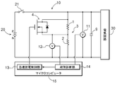
- Circuit block diagram schematically showing an example of the configuration of the discharge control circuit Circuit block diagram schematically showing an example of the configuration of a discharge control circuit with a diagnostic function Circuit block diagram showing an example of a discharge control circuit of a comparative example
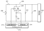
- the circuit block diagram which shows an example which added the diagnostic function to the discharge control circuit of another comparative example Circuit block diagram schematically showing another example of the configuration of the discharge control circuit
- the discharge control circuit 10 converts the electric charge accumulated in the smoothing capacitor 9 interposed between the main power source 20 that supplies DC power to the electric circuit 30 and the electric circuit 30 to the main power source 20. It is a circuit that discharges when the connection with the electric circuit 30 is disconnected.
- the electric circuit 30 can be a power system circuit such as an inverter or a converter that operates by consuming a large current of several A or more with a power supply voltage of a relatively high voltage (50 V or more).
- SMR system main relay
- the SMR 21 When the SMR 21 is closed, power is supplied from the main power supply 20 to the electric circuit 30, and when the SMR 21 is open, the connection between the main power supply 20 and the electric circuit 30 is disconnected.
- the electric circuit 30 When the electric circuit 30 is connected to the generator and the main power supply 20 is a rechargeable battery, the main power supply 20 may be charged by supplying power from the electric circuit 30 to the main power supply 20. .
- a smoothing capacitor 9 is provided between the main power supply 20 that supplies power and the electric circuit 30 in order to stabilize the power. Even when the SMR 21 is opened and the supply of power from the main power supply 20 is interrupted, the electric charge remains in the smoothing capacitor 9. This electric charge gradually decreases due to natural discharge, but when the electric circuit 30 is a power circuit as described above, the electrostatic capacity of the smoothing capacitor 9 also increases accordingly. The time to do also becomes long.
- the electric circuit 30 is inspected after the supply of power from the main power supply 20 is cut off, it is preferable that the electric charge of the smoothing capacitor 9 is discharged quickly. From such a viewpoint, a resistor is provided in parallel with the smoothing capacitor 9 in order to quickly discharge the electric charge of the smoothing capacitor 9.
- a resistor series portion 3 constituted by connecting a first resistor 1 and a second resistor 2 in series is connected in parallel to the smoothing capacitor 9.
- the smoothing capacitor 9 is charged with a transient response (charging characteristic) corresponding to a time constant determined by the combined resistance of the resistor series unit 3 and the capacitance of the smoothing capacitor 9.
- the voltage across the smoothing capacitor 9 becomes the voltage PN between the positive and negative electrodes of the main power supply 20.
- the voltage across the smoothing capacitor 9 can be expressed as P [V].
- the discharge control circuit 10 of the present embodiment is configured to be able to change the resistance value of the resistor series portion 3 at the start of charging, at the time of steady operation, and at the time of discharging.
- the resistance value of the resistor series unit 3 is a resistance value (sum) obtained by combining the resistance values of the first resistor 1 and the second resistor 2 connected in series. Become. On the other hand, at the time of discharging, the resistance value of the second resistor 2 becomes the resistance value of the resistor series portion 3. Such switching of the resistance value is performed as follows.
- the first resistor 1 is connected to the positive electrode P side of the main power supply 20, and the second resistor 2 is connected to the negative electrode N side.
- the first resistor 1 is a high-side resistor of the resistor series portion 3, and the second resistor 2 is a low-side resistor.
- the first resistor 1 is connected in parallel with a MOSFET 4 that functions as a switch.
- the MOSFET 4 is switching-controlled by a rapid discharge control unit 13 configured by, for example, a microcomputer. Specifically, the MOSFET 4 is controlled to be in a non-conducting state (off state) when the connection between the main power source 20 and the electric circuit 30 is maintained (when the SMR 21 is in a closed state). Further, the MOSFET 4 is controlled to be in a conductive state (on state) when the connection between the main power source 20 and the electric circuit 30 is disconnected (when the SMR 21 is in an open state).
- both ends of the first resistor 1 are connected via a minute on-resistance.
- the on-resistance is negligibly small with respect to the resistance value of the first resistor 1, and both ends of the first resistor 1 are substantially short-circuited.
- the resistance value of the resistor series part 3 becomes substantially the same as the resistance value of the second resistor 2.
- the SMR 21 is in an open state, and no charge is supplied from the main power supply 20 to the smoothing capacitor 9, and the charge accumulated in the smoothing capacitor 9 is discharged via the resistor series unit 3.
- the resistor series part 3 is composed only of the second resistor 2, the resistance value of the resistor series part 3 is smaller and the time constant is smaller than that during charging. Accordingly, the smoothing capacitor 9 is quickly discharged.
- the resistance value of the second resistor 2 is set to a value smaller than the resistance value of the first resistor 1. Since the resistance value of the resistance series part 3 at the time of discharging can be made smaller than at the time of charging or during steady state, the time constant can also be made smaller and the discharging of the smoothing capacitor 9 can be completed more quickly.
- the first resistor 1 and the second resistor 2 may be resistors having the same rated resistance value, and the resistance value of the first resistor 1 is the resistance value of the second resistor. It may be a smaller value.
- the resistance series part can be obtained by substantially short-circuiting both ends of the first resistor 1 via the MOSFET 4. It is possible to change the resistance value of 3 to a small value.
- the discharge control circuit 10 is configured such that the second resistor 2 is disposed outside the substrate.
- the second resistor 2 is disposed outside the substrate. Specifically, by connecting a connector assembly including the second resistor 2 to the connector housing mounted on the board, between the negative electrode N side and the parallel portion of the first resistor 1 and the MOSFET 4. It is preferable that the second resistor 2 is mounted.
- the second resistor 2 By disposing the second resistor 2 outside the substrate, heat dissipation of the second resistor 2 can be realized with a high degree of freedom such as addition of a heat sink including simple air cooling. In addition, the second resistor 2 can be easily replaced by replacing the connector assembly.
- the first resistor 1 and the MOSFET 4 are arranged on the high side of the resistor series portion 3.
- the terminals partially exposed to the outside of the substrate through the connector housing are the negative electrode N side of the main power supply 20 and the terminals opposite to the first resistor 1 and the positive electrode P side of the MOSFET 4. . Therefore, the terminal on the positive electrode P side of the main power supply 20 can be mounted with high insulation on the substrate without being partially exposed to the outside of the substrate.
- the main power supply 20 has a large voltage of, for example, 50 V or more, it is preferable that insulation on the positive electrode P side is particularly strictly implemented in consideration of safety.
- FIG. 3 shows a discharge control circuit 100 as a comparative example with respect to the discharge control circuit 10 of the present embodiment.
- the first resistor 101 that functions during steady operation of the electric circuit 130 and the discharge of the smoothing capacitor 109 and the second resistor 102 that functions during the discharge of the smoothing capacitor 109 are respectively connected to the smoothing capacitor 109.
- P [V] which is a voltage between the positive and negative electrodes of the main power supply 120
- the voltage applied between the drain and the source is P [V] as the first resistor 1 and the second resistor 2.
- P [V] the voltage applied between the drain and the source
- the present embodiment illustrated in FIG. 1 when the MOSFET 4 is in the OFF state, the voltage applied between the drain and the source is P [V] as the first resistor 1 and the second resistor 2. And is a voltage lower than P [V].
- the drain-source voltage is P ⁇ (R1 / (R1 + R2)) [V]. is there. That is, in the discharge control circuit 10 of the present embodiment, the voltage across the MOSFET 4 can be kept low, so that an element with a low withstand voltage can be used, and an increase in device scale and cost can be suppressed.
- FIG. 2 shows an example in which such a diagnostic circuit is added to the discharge control circuit 10 of FIG.
- the discharge control circuit 10 includes a first voltage sensor 11 that detects a voltage at a terminal on the positive electrode P side of the resistor series unit 3, a first resistor 1, and a second resistor 2.
- a second voltage sensor 12 for detecting the voltage at the connection point is provided.
- the detection results by the first voltage sensor 11 and the second voltage sensor 12 are transmitted to the failure diagnosis unit 14 configured using the microcomputer 15, similarly to the rapid discharge control unit 13.
- the failure diagnosis unit 14 diagnoses the failure of the resistor series unit 3 and the MOSFET 4 based on the detection result of the first voltage sensor 11 and the detection result of the second voltage sensor 12.
- the failure diagnosis unit 14 determines the first resistor 1 based on the detection result of the first voltage sensor 11. And the voltage at the connection point of the second resistor 2 can be calculated. Then, based on the calculation result and the detection result of the second voltage sensor 12, it can be determined whether or not the resistance series portion 3 (including the MOSFET 4) is normal.
- the failure diagnosis unit 14 can determine that the resistor series unit 3 has a failure (a power fault). If the terminal on the negative electrode N side of the first resistor 1 or MOSFET 4 (the terminal on the positive electrode P side of the second resistor 2) is short-circuited to the negative electrode N, the detection value of the second voltage sensor 12 is 0. [V]. In this case, the failure diagnosis unit 14 can determine that the resistor series unit 3 has a failure (ground fault).
- the failure diagnosis unit 14 can determine that the first resistor 1 has a failure (open failure).
- the detection value of the second voltage sensor 12 is P [V Therefore, the failure diagnosis unit 14 can determine that the second resistor 2 has a failure (open failure).
- the failure diagnosis unit 14 does not necessarily specify the type of failure, and it is sufficient if it can determine whether or not there is a failure.
- the fault diagnosis unit 14 controls the MOSFET 4 to be in the ON state by the rapid discharge control unit 13 when the SMR 21 is in the closed state
- the detection value of the second voltage sensor 12 does not become P [V], and P ⁇ In the case of (R1 / (R1 + R2))
- the failure diagnosis of the resistor series unit 3 including the MOSFET 4 as a switch can be executed. Reliability is improved.
- the failure diagnosis unit 14 can execute a failure diagnosis of the discharge control circuit 10 including the discharge characteristics of the smoothing capacitor 9.
- the failure diagnosing unit 14 monitors the detection values of the first voltage sensor 11 and the second voltage sensor 12 at a constant sampling interval while the MOSFET 4 is in an off state, so that the discharge characteristics of normal discharge that is not rapid discharge are detected. Can be obtained.
- a reference value of this discharge characteristic is stored in a program memory or parameter memory (not shown) of the microcomputer 15 and the obtained discharge characteristic is compared with this reference value, so that the discharge control circuit 10 including the discharge characteristic is included. Fault diagnosis is possible.
- the microcomputer 15 can acquire the discharge characteristics at the time of rapid discharge by monitoring the detection values of the first voltage sensor 11 and the second voltage sensor 12 at a constant sampling interval with the MOSFET 4 turned on. Similarly, by comparing the obtained discharge characteristic with the reference value of the discharge characteristic at the time of rapid discharge stored in the program memory or parameter memory of the microcomputer 15, the discharge characteristic including the discharge characteristic at the time of rapid discharge is also included. A failure diagnosis of the control circuit 10 can be performed.
- the discharge characteristics of normal discharge that is not rapid discharge can be obtained as described above. Further, when the MOSFET 104 is in the ON state, the discharge characteristics of the rapid discharge can be acquired as described above. These discharge characteristics can be compared with reference values by the microcomputer 115 in the same manner as described above. Further, although detailed description is omitted, a ground fault of the terminal on the negative electrode N side of the second resistor 102 can also be detected.
- the discharge control circuit 100 cannot detect the open failure due to the disconnection of the first resistor 101 as well as the acquisition of the discharge characteristics as described above.
- the discharge control circuit 100 it is necessary to configure the discharge control circuit 100 as shown in at least FIG. Specifically, the first resistor 101 has a configuration in which two resistors 101a and 101b are connected in series. Then, it is necessary to further include a third voltage sensor 119 at the connection point between the resistor 101a and the resistor 101b, and to transmit the detection result to the failure diagnosis unit 114.
- the failure diagnosis unit 114 diagnoses the failure of the discharge control circuit 100 based on the detection results of the first voltage sensor 111, the second voltage sensor 112, and the third voltage sensor 119.
- the detection result of the first voltage sensor 111 is P [V].
- the discharge control circuit 10 shown in FIG. 2 As is clear from a comparison between the discharge control circuit 10 shown in FIG. 2 and the discharge control circuit 100 shown in FIG. 4, in the discharge control circuit 100 of the comparative example, the first resistor 101 is divided into two, The circuit scale increases, for example, by providing the third voltage sensor 119. Therefore, the discharge control circuit 10 which is one embodiment of the present invention illustrated in FIG. 2 is preferable because the same function can be configured on a smaller scale.
- the discharge control circuit 100 as a comparative example can be configured as a discharge control circuit 200 shown in FIG. 5 by replacing the MOSFET 104 from the low side to the high side.
- a current sensor 218 as a sensor that provides detection information to the failure diagnosis unit 214.
- the current sensor 218 detects an overcurrent that flows when the MOSFET 204 is turned on in a state in which the positive electrode P side of the second resistor 202 has a ground fault.
- the discharge control circuit 200 when the MOSFET 204 is in the off state, the rapid discharge function cannot be diagnosed including the state of the second resistor 202.
- the discharge control circuit 200 cannot detect an open failure of the second resistor 202.
- the discharge control circuit 10 according to one aspect of the present invention can detect both the ground fault and the open fault of the second resistor 2 when the MOSFET 4 is in the OFF state.
- the discharge control circuit 10 does not have a function of detecting these failures when the MOSFET 4 is on, a ground fault of the second resistor 2 can be detected when the MOSFET 4 is off. Therefore, if the MOSFET 4 is not controlled to be in the ON state, a short circuit can be avoided. That is, it is possible to prevent an overcurrent from flowing through the MOSFET 4, to prevent the MOSFET 4 from being damaged, and to discharge the remaining charge of the smoothing capacitor 9 through at least the first resistor 1.
- the present invention is not limited to this configuration.
- the first resistor 1 and the MOSFET 4 may be disposed on the low side of the resistor series unit 3.
- the discharge control circuit 10 may also be configured with a failure diagnosis function, similar to the discharge control circuit 10 illustrated in FIG.
- the present invention can be applied to a discharge control circuit that discharges charges accumulated in a smoothing capacitor.
- the present invention is preferably applied to a discharge control circuit that effectively discharges a smoothing capacitor of a power electric circuit that operates at a large voltage and a large current.
- an electric circuit for example, an inverter for driving a rotating electrical machine, a DC-DC converter, or the like can be applied.
- First resistor 2 Second resistor 3: Resistor series part 4: MOSFET (switch) 10: discharge control circuit 11: first voltage sensor 12: second voltage sensor 14: failure diagnosis unit 20: main power supply 30: electric circuit
Landscapes
- Engineering & Computer Science (AREA)
- Power Engineering (AREA)
- Inverter Devices (AREA)
- Protection Of Static Devices (AREA)
- Charge And Discharge Circuits For Batteries Or The Like (AREA)
- Dc-Dc Converters (AREA)
Abstract
電力供給時の電力消費が小さく、電源遮断時には平滑コンデンサに蓄積された電荷を速やかに放電させることが可能であり、放電を制御するスイッチの耐圧が低い放電制御回路を提供する。第1抵抗器1と第2抵抗器2とが直列接続されていると共に、平滑コンデンサ9に対して並列に接続されている抵抗直列部3と、第1抵抗器1と並列に接続されると共に、主電源20と電気回路30との接続が維持されている際には非導通状態であり、主電源20と電気回路30との接続が切断された際には導通状態で第1抵抗器1の両端を短絡させるスイッチ4とを備え、主電源20と電気回路30との間に介在された平滑コンデンサ9の電荷を、主電源20と電気回路30接続が切断された際に放電させる。
Description
本発明は、平滑コンデンサに蓄積された電荷を放電させる放電制御回路に関する。
電気回路は、当該回路を動作させる電力を供給されて所定の機能を実現する。この電力が安定していなければ、回路の動作の安定性も低くなるので、多くの場合、電力を供給する電源と電気回路と間に、当該電力を安定させるために平滑コンデンサが備えられる。電源からの電力の供給が遮断された場合でも、この平滑コンデンサには電荷が蓄積されており、この電荷は自然放電によって次第に減少する。但し、電気回路が50V以上の比較的高電圧且つ数A以上の消費電流で動作する場合には、平滑コンデンサの静電容量もそれに応じて大きくなるから、自然放電によって電荷が減少する時間も長くなる。電源からの電力の供給が遮断された後に、電気回路を点検するようなことも考慮すると、平滑コンデンサの電荷は速やかに放電されることが好ましい。このような観点から、平滑コンデンサの電荷を速やかに放電させるために、平滑コンデンサと並列に放電抵抗が備えられる場合がある。当然ながら、この放電抵抗の抵抗値が小さい方が、放電に要する時間は短くなる。しかし、放電抵抗の抵抗値が小さいほど、電力が供給された状態での消費電力が大きくなる(効率が悪化する)とともに、抵抗器の外形も大きくなる。そのため従来のシステムでは比較的放電時間の長い放電抵抗が用いられている場合が多い(この放電は常時放電と称す。)。しかし、点検、安全性向上の観点からこれとは別に電力の遮断の際にのみ機能する急速放電システムの追加も必要となってきている。
特開平6-276610号公報(特許文献1)には、スイッチとして機能するメカニカルリレーにより、平滑コンデンサの充放電を制御する技術が開示されている(第17-19段落、図1等)。これによれば、平滑コンデンサ(C)を充電する際には、放電抵抗(R1)がメカニカルリレー(Ry3)により遮断され、平滑コンデンサ(C)への突入電流を抑制する電流制限抵抗(充電用抵抗(R2))を介して平滑コンデンサ(C)に電荷が供給される。この充電用抵抗(R2)は、電源投入時を除いてメカニカルリレー(Ry2)により遮断される。一方、平滑コンデンサ(C)を放電させる際には、平滑コンデンサ(C)に対する放電抵抗(R1)との並列接続がメカニカルリレー(Ry3)により確立され、平滑コンデンサ(C)に蓄積された電荷が放電抵抗(R1)を介して放電される。
ところで、このような放電回路においてスイッチとして機能する素子には、メカニカルリレー以外にも、半導体を用いたソリッドステートリレーや、FETなどの半導体スイッチング素子がある。そして、昨今では、取り扱いの容易さや、コストの観点から、このような半導体を用いたスイッチが利用されることが多い。このようなスイッチが遮断状態にある時には、その接点には電圧が掛かることになる。メカニカルリレーでは、接点の物理的な離間距離が絶縁距離となり、これが耐圧となる。半導体によるスイッチでは、例えばPN接合などの逆降伏電圧が耐圧となる。ここで、電源から電力を供給される電気回路の動作電圧が例えば50V以上の比較的高電圧である場合には、平滑コンデンサの両端電圧も同様に50V以上の比較的高電圧となる。また、電気回路が回転電機などの駆動回路であれば、動作電圧は、200V以上となる場合もある。平滑コンデンサに対して並列に接続される放電抵抗の両端電圧は、平滑コンデンサの両端電圧と等価となるから、放電抵抗を遮断するスイッチのオフ状態における接点にも同様の電圧が掛かる。従って、スイッチには高い耐圧特性が要求される。但し、そのような高い耐圧特性を有する半導体スイッチは、大型であったり、高コストであったりする可能性がある。
上記背景に鑑みて、電力供給時の電力消費を小さくすると共に、電源遮断時には当該平滑コンデンサに蓄積された電荷を速やかに放電させることが可能であり、放電を制御するスイッチの耐圧が低く抑えられた放電制御回路の提供が望まれる。
上記課題に鑑みた本発明に係る放電制御回路の特徴構成は、
電気回路へ直流電力を供給する主電源と当該電気回路との間に介在された平滑コンデンサに蓄積された電荷を、前記主電源と前記電気回路との接続が切断された際に放電させる放電制御回路であって、
第1抵抗器と第2抵抗器とが直列接続されて構成されていると共に、前記平滑コンデンサに対して並列に接続されている抵抗直列部と、
前記第1抵抗器と並列に接続されると共に、前記主電源と前記電気回路との接続が維持されている際には非導通状態に制御され、前記主電源と前記電気回路との接続が切断された際には導通状態に制御されて前記第1抵抗器の両端を短絡させるスイッチと、
を備える点にある。
電気回路へ直流電力を供給する主電源と当該電気回路との間に介在された平滑コンデンサに蓄積された電荷を、前記主電源と前記電気回路との接続が切断された際に放電させる放電制御回路であって、
第1抵抗器と第2抵抗器とが直列接続されて構成されていると共に、前記平滑コンデンサに対して並列に接続されている抵抗直列部と、
前記第1抵抗器と並列に接続されると共に、前記主電源と前記電気回路との接続が維持されている際には非導通状態に制御され、前記主電源と前記電気回路との接続が切断された際には導通状態に制御されて前記第1抵抗器の両端を短絡させるスイッチと、
を備える点にある。
この構成によれば、第1抵抗器と並列に接続されるスイッチの両端には、平滑コンデンサの端子間電圧を第1抵抗器と第2抵抗器とで分圧した電圧が印加される。つまり、スイッチの両端には、平滑コンデンサの端子間電圧よりも小さい電圧が印加されることになる。従って、耐圧が平滑コンデンサの端子間電圧よりも小さい電気的特性を有するスイッチを利用することができる。また、電力供給時は、直列接続された第1抵抗器と第2抵抗器との抵抗値の和が合成抵抗となるから、電力消費は小さい。一方、平滑コンデンサの電荷を放電する際には、第1抵抗器の両端がスイッチによって短絡され、第2抵抗器のみが放電抵抗となるので、小さい時定数で平滑コンデンサを放電させることができる。このように、本特徴構成によれば、電力供給時の電力消費を小さくすると共に、電源遮断時には当該平滑コンデンサに蓄積された電荷を速やかに放電させることが可能であり、放電を制御するスイッチの耐圧が抑制された放電制御回路を得ることができる。
ここで、本発明に係る放電制御回路の前記第2抵抗器の抵抗値は、前記第1抵抗器の抵抗値よりも小さい値に設定されていると好適である。この構成によれば、通常の電力供給時の電力消費を小さくするとともに、素早い放電が可能となる。
また、本発明に係る放電制御回路の前記第1抵抗器及び前記スイッチは、前記主電源の正極側に接続されていると好適である。この構成によれば、仮に第2抵抗器が地絡故障を生じた場合であっても、スイッチが開放状態であれば第1抵抗器が平滑コンデンサに対して並列接続されることになる。従って、第1抵抗器及びスイッチが、主電源の正極側に接続されていると、放電抵抗としての機能はこの第1抵抗器によって維持される。
また、急速放電の際に、大電流が流れ、発熱が大きい第2抵抗器の放熱を容易にするために、第1抵抗器やスイッチが実装される基板の外に第2抵抗器が配置されるように放電制御回路が構成される場合がある。例えば、基板に実装されたコネクタハウジングに、第2抵抗器を含むコネクタアッセンブリを接続することによってこの構成を実現することができる。この際、コネクタハウジングの端子を介して、基板の外に露出する可能性があるのは、主電源の負極側と、第1抵抗器及びスイッチの端子である。従って、上記構成によれば、大電圧である可能性もある主電源の正極は基板の中に収まり、絶縁を確保し易くなる。
ところで、第1抵抗器及びスイッチが主電源の正極側に接続されている場合に、平滑コンデンサを急速放電させるための第2抵抗器が地絡故障を生じると、地絡故障により放電抵抗としての機能を失うことになる。しかし、例えば、第1抵抗器と第2抵抗器との接続点の電圧をモニターしておくことによって、この地絡故障を検出することができる。即ち、第2抵抗器が地絡故障を生じていない場合には、当該接続点の電圧は、平滑コンデンサの両端電圧(主電源の電圧)を第1抵抗器と第2抵抗器とで分圧した値となる。一方、第2抵抗器が地絡故障を生じている場合には、当該接続点の電圧は、グラウンド電圧(主電源の負極側の電圧)となる。従って、放電制御回路は、電気回路の定常動作中に第2抵抗器が地絡故障を生じたとしても、第1抵抗器と第2抵抗器との接続点の電圧をモニターしておくことによって、この地絡故障を検出することができる。そして、放電制御回路は、スイッチをオン状態に制御しないようにすれば、スイッチに過電流が流れることを防止できスイッチの破損を防止できるとともに、少なくとも第1抵抗器を介して平滑コンデンサの電荷を放電させることが可能である。また、別の故障として、スイッチが短絡故障を生じている場合には、常に第1抵抗器が短絡状態となり、第1抵抗器と第2抵抗器との接続点の電圧が主電源の正極側の電圧となる。従って、当該接続点の電圧をモニターしておくことによって、スイッチの短絡故障や第1抵抗器の短絡故障も検出することができる。
具体的には、1つの好適な態様として、本発明に係る放電制御回路は、前記抵抗直列部の正極側端子の電圧を検出する第1電圧センサと、前記第1抵抗器と前記第2抵抗器との接続点の電圧を検出する第2電圧センサと、前記第1電圧センサの検出結果及び前記第2電圧センサの検出結果に基づいて、前記抵抗直列部及び前記スイッチの故障を診断する故障診断部とをさらに備えると好適である。尚、第1抵抗器及びスイッチが、主電源の正極側ではなく、負極側に接続されている場合であっても、第1電圧センサと第2電圧センサと故障診断部とを備えることによって、放電制御回路の故障を検出することが可能である。例えば、第1抵抗器が地絡故障を生じた場合には、当該接続点の電圧がグラウンド電圧(主電源の負極側の電圧)となるので、この地絡故障を検出することができる。
以下、本発明の実施形態を図面に基づいて説明する。放電制御回路10は、図1に示すように、電気回路30へ直流電力を供給する主電源20と電気回路30との間に介在された平滑コンデンサ9に蓄積された電荷を、主電源20と電気回路30との接続が切断された際に放電させる回路である。電気回路30は、種々の回路を適用することができる。例えば、電気回路30は、比較的高電圧(50V以上)の電源電圧で数A以上の大電流を消費して動作するようなインバータやコンバータなどのパワー系の回路とすることができる。このような電気回路30は、システムメインリレー(SMR)21等を介して主電源20と接続される。SMR21が閉じている場合には、主電源20から電気回路30に電力が供給され、SMR21が開放している場合には、主電源20と電気回路30との接続が切断される。尚、電気回路30が発電機に接続されており、主電源20が充電可能なバッテリーなどの場合には、電気回路30から主電源20に電力を供給して主電源20を充電してもよい。
ところで、電気回路30を動作させる電力が安定していなければ、当該電気回路30の動作の安定性も低くなる。従って、多くの場合、電力を供給する主電源20と電気回路30と間に、当該電力を安定させるために平滑コンデンサ9が備えられる。SMR21が開放され、主電源20からの電力の供給が遮断された場合でも、この平滑コンデンサ9には電荷が残存している。この電荷は自然放電によっても次第に減少するが、電気回路30が上述したようなパワー系の回路の場合には、平滑コンデンサ9の静電容量もそれに応じて大きくなるから、自然放電によって電荷が減少する時間も長くなる。主電源20からの電力の供給が遮断された後に、電気回路30を点検するようなケースも考慮すると、平滑コンデンサ9の電荷は速やかに放電されることが好ましい。このような観点から、平滑コンデンサ9の電荷を速やかに放電させるために、平滑コンデンサ9と並列に抵抗器が備えられる。
本実施形態においては、第1抵抗器1と第2抵抗器2とが直列接続されて構成された抵抗直列部3が平滑コンデンサ9に対して並列に接続されている。SMR21が開状態から閉状態となると、抵抗直列部3の合成抵抗と平滑コンデンサ9の静電容量とで定まる時定数に応じた過渡応答(充電特性)を伴って平滑コンデンサ9が充電される。充電が完了し、定常状態となると、平滑コンデンサ9の両端電圧は、主電源20の正負両極間電圧P-Nとなる。ここで、主電源20の負極Nをグラウンド(=0[V])とすれば、平滑コンデンサ9の両端電圧は、P[V]と表すことができる。
一方、SMR21が閉状態から開状態となると、平滑コンデンサ9に蓄積された電荷は、抵抗直列部3を介して放電される。この際、抵抗直列部3の抵抗値が小さいほど、電流は大きくなり、放電に要する時間は短くなる。しかし、抵抗直列部3の抵抗値が小さいと通常時の電力消費が大きくなってしまう。そこで、本実施形態の放電制御回路10は、充電開始時や定常動作時と、放電時とにおいて、抵抗直列部3の抵抗値を変更できるように構成されている。具体的には、充電開始時や定常動作時には、抵抗直列部3の抵抗値は、直列接続された第1抵抗器1と第2抵抗器2との抵抗値を合成した抵抗値(和)となる。一方、放電時には、第2抵抗器2の抵抗値が抵抗直列部3の抵抗値となる。このような抵抗値の切り換えは以下のようにして実施される。
図1に示すように、本実施形態では、主電源20の正極Pの側に第1抵抗器1が接続され、負極Nの側に第2抵抗器2が接続されている。換言すれば、第1抵抗器1は、抵抗直列部3のハイサイドの抵抗器であり、第2抵抗器2はローサイドの抵抗器である。また、第1抵抗器1には、スイッチとして機能するMOSFET4が並列に接続されている。このMOSFET4は、例えばマイクロコンピュータなどによって構成された急速放電制御部13によってスイッチング制御される。具体的には、MOSFET4は、主電源20と電気回路30との接続が維持されている際(SMR21が閉状態のとき)には非導通状態(オフ状態)に制御される。また、MOSFET4は、主電源20と電気回路30との接続が切断された際(SMR21が開状態のとき)には導通状態(オン状態)に制御される。
MOSFET4が導通状態に制御されると、微小なオン抵抗を介して第1抵抗器1の両端が接続される。このオン抵抗は、第1抵抗器1の抵抗値に対して無視できるほど小さく、実質的に第1抵抗器1の両端が短絡される。第1抵抗器1の両端がMOSFET4を介して短絡されることにより、抵抗直列部3の抵抗値は、実質的に第2抵抗器2の抵抗値と同じになる。SMR21は開放状態にあり、主電源20から平滑コンデンサ9には電荷が供給されず、平滑コンデンサ9に蓄積された電荷は、抵抗直列部3を介して放電される。この際、抵抗直列部3は第2抵抗器2のみで構成されているので、充電時に比べて抵抗直列部3の抵抗値は小さく、時定数も小さい。従って、迅速に平滑コンデンサ9の放電が完了する。
ここで、第2抵抗器2の抵抗値が、第1抵抗器1の抵抗値よりも小さい値に設定されていると好適である。充電時や定常時に比べて放電時の抵抗直列部3の抵抗値をより小さくすることができるので、時定数もより小さくすることができ、さらに迅速に平滑コンデンサ9の放電を完了させることができる。当然ながら、第1抵抗器1と第2抵抗器2とは、同じ定格値の抵抗値を有する抵抗器であってもよいし、第1抵抗器1の抵抗値が第2抵抗器の抵抗値よりも小さい値であってもよい。つまり、2つの抵抗器の抵抗値の和に比べれば、第2抵抗器2の抵抗値は小さいから、第1抵抗器1の両端をMOSFET4を介して実質的に短絡することによって、抵抗直列部3の抵抗値を小さい値へと変更することが可能である。
尚、急速放電の際に大電流が流れることから、第1抵抗器1に比べて発熱が大きい第2抵抗器2の放熱を容易にするために、第1抵抗器1やMOSFET4が実装される基板の外に第2抵抗器2が配置されるように放電制御回路10が構成されると好適である。また、発熱による消耗や定期的なメンテナンスにより、第2抵抗器2を交換する際も、当該基板の外に第2抵抗器2が配置されていると好適である。具体的には、当該基板に実装されたコネクタハウジングに、第2抵抗器2を含むコネクタアッセンブリを接続することによって、負極Nの側と、第1抵抗器1及びMOSFET4の並列部との間に第2抵抗器2が実装されると好適である。第2抵抗器2が基板外に配置されることによって、単純な空冷を含め、ヒートシンクの付加など、高い自由度で第2抵抗器2の放熱を実現することができる。また、当該コネクタアッセンブリを交換することによって、容易に第2抵抗器2を交換することも可能である。
図1に例示する放電制御回路10は、上述したように、抵抗直列部3のハイサイドに第1抵抗器1とMOSFET4(スイッチ)が配置されている。このため、コネクタハウジングを介して基板の外に部分的に露出する端子は、主電源20の負極Nの側と、第1抵抗器1及びMOSFET4の正極Pの側とは反対の端子とである。従って、主電源20の正極Pの側の端子は、部分的にも基板の外部に対して露出することなく、当該基板において高い絶縁性を保って実装されることが可能である。主電源20が例えば50V以上の大電圧の場合には、安全性を考慮して正極Pの側の絶縁は特に厳重に実施されることが好ましい。第1抵抗器1及びMSOFET4をハイサイドに配置することによって、そのような好適な形態を容易に実現することができる。
ところで、図3は、本実施形態の放電制御回路10に対する比較例となる放電制御回路100を示している。この放電制御回路100では、電気回路130の定常運転時及び平滑コンデンサ109の放電時に機能する第1抵抗器101と、平滑コンデンサ109の放電時に機能する第2抵抗器102とが、それぞれ平滑コンデンサ109に対して並列に接続されている。放電制御回路100では、MOSFET104がオフ状態の時、そのドレイン-ソース間に主電源120の正負両極間電圧であるP[V]が印可されることになる。これに対して、図1に例示した本実施形態では、MOSFET4がオフ状態のとき、そのドレイン-ソース間に印可される電圧は、P[V]を第1抵抗器1と第2抵抗器2とによって分圧した電圧であり、P[V]よりも低い電圧となる。
具体的には、第1抵抗器1の抵抗値をR1、第2抵抗器2の抵抗値をR2とすれば、ドレイン-ソース間電圧は、P×(R1/(R1+R2))[V]である。つまり、本実施形態の放電制御回路10では、MOSFET4の両端電圧を低く抑えることが可能となるので、耐圧の低い素子を用いることができ、装置規模やコストの増大を抑制可能である。上述したように、第2抵抗器2の抵抗値R2が第1抵抗器1の抵抗値R1よりも小さい場合、例えば、R1=45[kΩ]、R2=5[kΩ]、P=100[V]とすれば、MOSFET4のドレイン-ソース間電圧は、90[V]となる。図3に示す放電制御回路100のMOSFET104のドレイン-ソース間電圧はP=100[V]となるから、本実施形態の放電制御回路10のMOSFET4の方が、より低い耐圧の素子を用いることができる。
また、本実施形態の放電制御回路10は、優れた診断機能を付加することが可能である。図2は、図1の放電制御回路10にそのような診断回路を付加した例を示している。図2に示すように、放電制御回路10には、抵抗直列部3の正極Pの側の端子の電圧を検出する第1電圧センサ11と、第1抵抗器1と第2抵抗器2との接続点の電圧を検出する第2電圧センサ12とが備えられている。これら第1電圧センサ11と第2電圧センサ12とによる検出結果は、急速放電制御部13と同様に、マイクロコンピュータ15を用いて構成された故障診断部14に伝達される。故障診断部14は、第1電圧センサ11の検出結果及び第2電圧センサ12の検出結果に基づいて、抵抗直列部3及びMOSFET4の故障を診断する。
(診断条件/SMR:閉(定常動作中))
SMR21が閉状態の時、第1抵抗器1及び第2抵抗器2の抵抗値は既知であるから、第1電圧センサ11の検出結果に基づいて、故障診断部14は、第1抵抗器1と第2抵抗器2との接続点における電圧を演算することができる。そして、この演算結果と、第2電圧センサ12の検出結果に基づいて抵抗直列部3(MOSFET4も含む)が正常であるか否かを判定することができる。例えば、第1抵抗器1又はMOSFET4の負極Nの側の端子(又は第2抵抗器2の正極Pの側の端子)が正極Pに短絡していれば、第2電圧センサ12の検出値がP[V]となる。この場合、故障診断部14は、抵抗直列部3に故障(天絡故障)有りと判定することができる。また、第1抵抗器1又はMOSFET4の負極Nの側の端子(第2抵抗器2の正極Pの側の端子)が負極Nに短絡していれば、第2電圧センサ12の検出値が0[V]となる。この場合、故障診断部14は、抵抗直列部3に故障(地絡故障)有りと判定することができる。
SMR21が閉状態の時、第1抵抗器1及び第2抵抗器2の抵抗値は既知であるから、第1電圧センサ11の検出結果に基づいて、故障診断部14は、第1抵抗器1と第2抵抗器2との接続点における電圧を演算することができる。そして、この演算結果と、第2電圧センサ12の検出結果に基づいて抵抗直列部3(MOSFET4も含む)が正常であるか否かを判定することができる。例えば、第1抵抗器1又はMOSFET4の負極Nの側の端子(又は第2抵抗器2の正極Pの側の端子)が正極Pに短絡していれば、第2電圧センサ12の検出値がP[V]となる。この場合、故障診断部14は、抵抗直列部3に故障(天絡故障)有りと判定することができる。また、第1抵抗器1又はMOSFET4の負極Nの側の端子(第2抵抗器2の正極Pの側の端子)が負極Nに短絡していれば、第2電圧センサ12の検出値が0[V]となる。この場合、故障診断部14は、抵抗直列部3に故障(地絡故障)有りと判定することができる。
また、第1抵抗器1が断線したり、第1抵抗器1の端子が基板等から外れていたりしてオープン状態となっている場合には、第2電圧センサ12の検出値が0[V]となるから、故障診断部14は、第1抵抗器1に故障(オープン故障)有りと判定することができる。また、第2抵抗器2が断線したり、第2抵抗器2の端子が基板等から外れていたりしてオープン状態となっている場合には、第2電圧センサ12の検出値がP[V]となるから、故障診断部14は、第2抵抗器2に故障(オープン故障)有りと判定することができる。尚、故障診断部14は、必ずしも故障の種類までを特定する必要はなく、故障の有無を判定可能であれば充分である。
また、故障診断部14は、SMR21が閉状態の時に、急速放電制御部13によりMOSFET4をオン状態に制御しても、第2電圧センサ12の検出値がP[V]とならず、P×(R1/(R1+R2))の場合には、MOSFET4に故障有りと判定することができる。このように、SMR21が閉状態の時、つまり、電気回路30が定常動作している間に、スイッチとしてのMOSFET4を含む抵抗直列部3の故障診断を実行することができるので、放電制御回路10の信頼性が向上する。
(診断条件/SMR:開(放電動作中))
一方、SMR21が開状態の際には、故障診断部14は、平滑コンデンサ9の放電特性を含めて放電制御回路10の故障診断を実行することができる。例えば、故障診断部14は、MOSFET4がオフ状態のままで、一定のサンプリング間隔で第1電圧センサ11及び第2電圧センサ12の検出値をモニターすることで、急速放電ではない通常放電の放電特性を取得することができる。マイクロコンピュータ15の不図示のプログラムメモリやパラメータメモリにこの放電特性の基準値を記憶させておき、取得した放電特性とこの基準値とを比較することによって、放電特性も含めた放電制御回路10の故障診断が可能となる。また、マイクロコンピュータ15は、MOSFET4をオン状態として一定のサンプリング間隔で第1電圧センサ11及び第2電圧センサ12の検出値をモニターすることで、急速放電時の放電特性を取得することができる。そして、同様に、マイクロコンピュータ15のプログラムメモリやパラメータメモリに記憶された急速放電時の放電特性の基準値と取得した放電特性とを比較することによって、急速放電時の放電特性も含めて、放電制御回路10の故障診断を行うことができる。
一方、SMR21が開状態の際には、故障診断部14は、平滑コンデンサ9の放電特性を含めて放電制御回路10の故障診断を実行することができる。例えば、故障診断部14は、MOSFET4がオフ状態のままで、一定のサンプリング間隔で第1電圧センサ11及び第2電圧センサ12の検出値をモニターすることで、急速放電ではない通常放電の放電特性を取得することができる。マイクロコンピュータ15の不図示のプログラムメモリやパラメータメモリにこの放電特性の基準値を記憶させておき、取得した放電特性とこの基準値とを比較することによって、放電特性も含めた放電制御回路10の故障診断が可能となる。また、マイクロコンピュータ15は、MOSFET4をオン状態として一定のサンプリング間隔で第1電圧センサ11及び第2電圧センサ12の検出値をモニターすることで、急速放電時の放電特性を取得することができる。そして、同様に、マイクロコンピュータ15のプログラムメモリやパラメータメモリに記憶された急速放電時の放電特性の基準値と取得した放電特性とを比較することによって、急速放電時の放電特性も含めて、放電制御回路10の故障診断を行うことができる。
(比較例の放電制御回路の診断/診断条件/SMR:開(放電動作中))
図3に示した比較例の放電制御回路100では、SMR121が開状態の場合には、上記と同様に放電特性も含めて故障診断が可能である。この場合には、図4に示すように、第1抵抗器101の正極側端子の電圧を検出する第1電圧センサ111と、第2抵抗器102とMOSFET104との接続点の電圧を検出する第2電圧センサ112とが備えられる。そして、これら第1電圧センサ111と第2電圧センサ112との検出結果に基づいて、故障診断部114は放電制御回路100の故障を診断することが可能である。MOSFET104がオフ状態の時には、上記と同様に、急速放電ではない通常放電の放電特性を取得することができる。また、MOSFET104がオン状態の時には、上記と同様に、急速放電の放電特性を取得することができる。これらの放電特性は、上記を同様に、マイクロコンピュータ115によって、基準値と比較可能である。また、詳細な説明は省略するが、第2抵抗器102の負極Nの側の端子の地絡なども、検出可能である。
図3に示した比較例の放電制御回路100では、SMR121が開状態の場合には、上記と同様に放電特性も含めて故障診断が可能である。この場合には、図4に示すように、第1抵抗器101の正極側端子の電圧を検出する第1電圧センサ111と、第2抵抗器102とMOSFET104との接続点の電圧を検出する第2電圧センサ112とが備えられる。そして、これら第1電圧センサ111と第2電圧センサ112との検出結果に基づいて、故障診断部114は放電制御回路100の故障を診断することが可能である。MOSFET104がオフ状態の時には、上記と同様に、急速放電ではない通常放電の放電特性を取得することができる。また、MOSFET104がオン状態の時には、上記と同様に、急速放電の放電特性を取得することができる。これらの放電特性は、上記を同様に、マイクロコンピュータ115によって、基準値と比較可能である。また、詳細な説明は省略するが、第2抵抗器102の負極Nの側の端子の地絡なども、検出可能である。
(比較例の放電制御回路の診断/診断条件/SMR:閉(定常動作中))
SMR121が閉状態の場合、放電制御回路100は、上記のような放電特性の取得はもちろんのこと、第1抵抗器101の断線などによるオープン故障を検出することはできない。図2に例示した放電制御回路10と同様の故障検出を実現するためには、少なくとも図4に示したように放電制御回路100を構成する必要がある。具体的には、第1抵抗器101を2つの抵抗器101a,101bの直列接続による構成とする。そして、抵抗器101aと抵抗器101bとの接続点にさらに第3電圧センサ119を備え、その検出結果を故障診断部114に伝達する必要がある。故障診断部114は、第1電圧センサ111と第2電圧センサ112と第3電圧センサ119との検出結果に基づいて、放電制御回路100の故障を診断する。詳細な説明は省略するが、第1抵抗器101(101a、101b)が正常であれば、第1電圧センサ111の検出結果はP[V]である。また、既知の値である第1抵抗器101aと101bとでP[V]が分圧された値が、第3電圧センサ119の検出結果である。第1抵抗器101aと101bとの何れかがオープン故障を生じていれば、第3電圧センサ119の検出結果が予想値(基準値)と異なることになる。従って、これによって、第1抵抗器101の故障を判定することができる。
SMR121が閉状態の場合、放電制御回路100は、上記のような放電特性の取得はもちろんのこと、第1抵抗器101の断線などによるオープン故障を検出することはできない。図2に例示した放電制御回路10と同様の故障検出を実現するためには、少なくとも図4に示したように放電制御回路100を構成する必要がある。具体的には、第1抵抗器101を2つの抵抗器101a,101bの直列接続による構成とする。そして、抵抗器101aと抵抗器101bとの接続点にさらに第3電圧センサ119を備え、その検出結果を故障診断部114に伝達する必要がある。故障診断部114は、第1電圧センサ111と第2電圧センサ112と第3電圧センサ119との検出結果に基づいて、放電制御回路100の故障を診断する。詳細な説明は省略するが、第1抵抗器101(101a、101b)が正常であれば、第1電圧センサ111の検出結果はP[V]である。また、既知の値である第1抵抗器101aと101bとでP[V]が分圧された値が、第3電圧センサ119の検出結果である。第1抵抗器101aと101bとの何れかがオープン故障を生じていれば、第3電圧センサ119の検出結果が予想値(基準値)と異なることになる。従って、これによって、第1抵抗器101の故障を判定することができる。
図2に示す放電制御回路10と、図4に示す放電制御回路100とを比較すれば明らかなように、比較例の放電制御回路100では、第1抵抗器101を2つに分割したり、第3電圧センサ119を設けたりするなど、回路規模が増大する。従って、図2に例示した、本発明の一態様である放電制御回路10は、同様の機能をより小規模に構成することができて好適である。
(比較例の放電制御回路の別の例)
尚、比較例としての放電制御回路100は、MOSFET104を、ローサイドからハイサイドに置き換えて、図5に示す放電制御回路200のように構成することもできる。この場合には、故障診断部214へ検出情報を提供するセンサとして、電流センサ218を備えると好適である。この電流センサ218は、例えば、第2抵抗器202の正極Pの側が地絡故障している状態でMOSFET204をオンにした際に流れる過電流を検出する。但し、この放電制御回路200では、MOSFET204がオフ状態の時には、第2抵抗器202の状態を含め、急速放電機能の診断は実施することができない。また、放電制御回路200では、第2抵抗器202のオープン故障も検出することはできない。これに対して、本発明の一態様である放電制御回路10は、上述したように、MOSFET4がオフ状態において第2抵抗器2の地絡故障も、オープン故障も検出可能である。尚、放電制御回路10は、MOSFET4がオンの状態で、これらの故障を検出する機能は有していないが、第2抵抗器2の地絡故障は、MOSFET4がオフの状態で検出可能であるから、MOSFET4をオン状態に制御しなければ、短絡を回避することができる。つまり、MOSFET4に過電流が流れることを防止できMOSFET4の破損を防止できると共に、少なくとも第1抵抗器1を介して平滑コンデンサ9の残存電荷を放電させることができる。
尚、比較例としての放電制御回路100は、MOSFET104を、ローサイドからハイサイドに置き換えて、図5に示す放電制御回路200のように構成することもできる。この場合には、故障診断部214へ検出情報を提供するセンサとして、電流センサ218を備えると好適である。この電流センサ218は、例えば、第2抵抗器202の正極Pの側が地絡故障している状態でMOSFET204をオンにした際に流れる過電流を検出する。但し、この放電制御回路200では、MOSFET204がオフ状態の時には、第2抵抗器202の状態を含め、急速放電機能の診断は実施することができない。また、放電制御回路200では、第2抵抗器202のオープン故障も検出することはできない。これに対して、本発明の一態様である放電制御回路10は、上述したように、MOSFET4がオフ状態において第2抵抗器2の地絡故障も、オープン故障も検出可能である。尚、放電制御回路10は、MOSFET4がオンの状態で、これらの故障を検出する機能は有していないが、第2抵抗器2の地絡故障は、MOSFET4がオフの状態で検出可能であるから、MOSFET4をオン状態に制御しなければ、短絡を回避することができる。つまり、MOSFET4に過電流が流れることを防止できMOSFET4の破損を防止できると共に、少なくとも第1抵抗器1を介して平滑コンデンサ9の残存電荷を放電させることができる。
〔その他の実施形態〕
本発明のその他の実施形態について説明する。なお、以下に説明する各実施形態の構成は、それぞれ単独で適用されるものに限られず、矛盾が生じない限り、他の実施形態の構成と組み合わせて適用することも可能である。
本発明のその他の実施形態について説明する。なお、以下に説明する各実施形態の構成は、それぞれ単独で適用されるものに限られず、矛盾が生じない限り、他の実施形態の構成と組み合わせて適用することも可能である。
(1)図1及び図2を用いて説明したように、本発明の一態様として抵抗直列部3のハイサイドに第1抵抗器1とMOSFET4(スイッチ)を配置する例を提示した。しかし、本発明はこの構成に限定されるものではない。例えば、図6に示すように、抵抗直列部3のローサイドに第1抵抗器1とMOSFET4が配置されてもよい。また、この放電制御回路10も図2に例示した放電制御回路10と同様に、故障診断機能を有して構成されてもよい。
(2)上記実施形態においては、第1抵抗器1と並列に配置されるスイッチとしてMOSFETを用いる例を示したが、本発明はこれに限定されるものではない。バイポーラトランジスタや、ソリッドステートリレー、メカニカルリレーなどを当該スイッチとして適用してもよい。
本発明は、平滑コンデンサに蓄積された電荷を放電させる放電制御回路に適用することができる。特に、大電圧大電流で動作するパワー系の電気回路の平滑コンデンサを効果的に放電させる放電制御回路に適用すると好適である。そのような電気回路として、例えば、回転電機を駆動するためのインバータや、DC-DCコンバータなどが適用できる。
1:第1抵抗器
2:第2抵抗器
3:抵抗直列部
4:MOSFET(スイッチ)
10:放電制御回路
11:第1電圧センサ
12:第2電圧センサ
14:故障診断部
20:主電源
30:電気回路
2:第2抵抗器
3:抵抗直列部
4:MOSFET(スイッチ)
10:放電制御回路
11:第1電圧センサ
12:第2電圧センサ
14:故障診断部
20:主電源
30:電気回路
Claims (4)
- 電気回路へ直流電力を供給する主電源と当該電気回路との間に介在された平滑コンデンサに蓄積された電荷を、前記主電源と前記電気回路との接続が切断された際に放電させる放電制御回路であって、
第1抵抗器と第2抵抗器とが直列接続されて構成されていると共に、前記平滑コンデンサに対して並列に接続されている抵抗直列部と、
前記第1抵抗器と並列に接続されると共に、前記主電源と前記電気回路との接続が維持されている際には非導通状態に制御され、前記主電源と前記電気回路との接続が切断された際には導通状態に制御されて前記第1抵抗器の両端を短絡させるスイッチと、
を備える放電制御回路。 - 前記第2抵抗器の抵抗値は、前記第1抵抗器の抵抗値よりも小さい値に設定されている請求項1に記載の放電制御回路。
- 前記第1抵抗器及び前記スイッチは、前記主電源の正極側に接続されている請求項1又は2に記載の放電制御回路。
- 前記抵抗直列部の正極側端子の電圧を検出する第1電圧センサと、
前記第1抵抗器と前記第2抵抗器との接続点の電圧を検出する第2電圧センサと、
前記第1電圧センサの検出結果及び前記第2電圧センサの検出結果に基づいて、前記抵抗直列部及び前記スイッチの故障を診断する故障診断部と、
をさらに備える請求項1から3の何れか一項に記載の放電制御回路。
Priority Applications (2)
| Application Number | Priority Date | Filing Date | Title |
|---|---|---|---|
| DE112012000652T DE112012000652T5 (de) | 2011-04-25 | 2012-03-29 | Entladesteuerungsschaltung |
| CN2012800114961A CN103444067A (zh) | 2011-04-25 | 2012-03-29 | 放电控制电路 |
Applications Claiming Priority (2)
| Application Number | Priority Date | Filing Date | Title |
|---|---|---|---|
| JP2011096839A JP2012231556A (ja) | 2011-04-25 | 2011-04-25 | 放電制御回路 |
| JP2011-096839 | 2011-04-25 |
Publications (1)
| Publication Number | Publication Date |
|---|---|
| WO2012147448A1 true WO2012147448A1 (ja) | 2012-11-01 |
Family
ID=47020786
Family Applications (1)
| Application Number | Title | Priority Date | Filing Date |
|---|---|---|---|
| PCT/JP2012/058380 Ceased WO2012147448A1 (ja) | 2011-04-25 | 2012-03-29 | 放電制御回路 |
Country Status (5)
| Country | Link |
|---|---|
| US (1) | US20120268079A1 (ja) |
| JP (1) | JP2012231556A (ja) |
| CN (1) | CN103444067A (ja) |
| DE (1) | DE112012000652T5 (ja) |
| WO (1) | WO2012147448A1 (ja) |
Cited By (2)
| Publication number | Priority date | Publication date | Assignee | Title |
|---|---|---|---|---|
| JP2015116097A (ja) * | 2013-12-13 | 2015-06-22 | 本田技研工業株式会社 | 放電回路故障検知装置及び放電回路故障検知方法 |
| JP2020182357A (ja) * | 2019-04-26 | 2020-11-05 | 株式会社オートネットワーク技術研究所 | 制御装置 |
Families Citing this family (37)
| Publication number | Priority date | Publication date | Assignee | Title |
|---|---|---|---|---|
| EP2481138A4 (en) * | 2009-09-23 | 2014-06-04 | Hewlett Packard Development Co | CURRENT CURRENT TOLERANCE ALLOCATION TO AN ELECTRONIC DEVICE |
| JP5298158B2 (ja) * | 2011-04-27 | 2013-09-25 | 本田技研工業株式会社 | 電源装置 |
| ITTO20110769A1 (it) * | 2011-08-12 | 2013-02-13 | Magneti Marelli Spa | Dispositivo e metodo di scarica per un condensatore in un impianto elettrico di potenza di un veicolo con trazione elettrica |
| JP5973322B2 (ja) * | 2012-10-31 | 2016-08-23 | 東芝シュネデール・インバータ株式会社 | インバータ装置の蓄積電力放電回路 |
| JP5686145B2 (ja) * | 2013-01-29 | 2015-03-18 | トヨタ自動車株式会社 | 電気自動車用の電力変換装置 |
| JP2014166033A (ja) * | 2013-02-25 | 2014-09-08 | Toyota Motor Corp | 電源装置 |
| DE102014202602A1 (de) * | 2013-11-15 | 2015-05-21 | Robert Bosch Gmbh | Verfahren zum Betreiben einer elektrischen Maschine |
| CN105337322B (zh) * | 2014-06-30 | 2017-11-07 | 南京德朔实业有限公司 | 一种充电组合 |
| JP6107836B2 (ja) * | 2015-01-07 | 2017-04-05 | トヨタ自動車株式会社 | 電池監視装置 |
| KR102003461B1 (ko) * | 2015-09-04 | 2019-07-24 | 엘에스산전 주식회사 | 전기 자동차 충전기 |
| JP6357722B2 (ja) * | 2015-12-22 | 2018-07-18 | 株式会社ケーヒン | 放電制御装置 |
| US10682694B2 (en) * | 2016-01-14 | 2020-06-16 | Glassimetal Technology, Inc. | Feedback-assisted rapid discharge heating and forming of metallic glasses |
| JP2017146260A (ja) * | 2016-02-19 | 2017-08-24 | 株式会社ケーヒン | 電圧検出装置 |
| WO2018034134A1 (ja) * | 2016-08-19 | 2018-02-22 | 三菱電機株式会社 | コンデンサの放電回路 |
| JP6658403B2 (ja) | 2016-08-29 | 2020-03-04 | 株式会社Ihi | 送電装置 |
| US10632529B2 (en) | 2016-09-06 | 2020-04-28 | Glassimetal Technology, Inc. | Durable electrodes for rapid discharge heating and forming of metallic glasses |
| DE102016222632A1 (de) * | 2016-11-17 | 2018-05-17 | Zf Friedrichshafen Ag | Vorrichtung und Verfahren zum Entladen eines Zwischenkreiskondensators |
| DE102016123209A1 (de) * | 2016-12-01 | 2018-06-07 | Lisa Dräxlmaier GmbH | Entladevorrichtung, elektrischer zwischenkreis und entladeverfahren |
| JP6664311B2 (ja) * | 2016-12-14 | 2020-03-13 | 三菱電機株式会社 | 駆動システムおよび電力変換装置 |
| JP6893813B2 (ja) * | 2017-03-29 | 2021-06-23 | Fdk株式会社 | リフレッシュ放電装置 |
| DE102017209100A1 (de) * | 2017-05-31 | 2018-12-06 | Robert Bosch Gmbh | Enladeschaltung und Verfahren zur Entladung eines Hochvolt-Zwischenkreises eines Fahrzeugs |
| DE102017209106A1 (de) * | 2017-05-31 | 2018-12-06 | Robert Bosch Gmbh | Verfahren und Vorrichtung zur Entladung eines Hochvolt-Zwischenkreises eines Fahrzeuges mit einer Entladeschaltung |
| CN110832334B (zh) * | 2017-06-20 | 2022-09-27 | 株式会社杰士汤浅国际 | 故障诊断装置 |
| CN107302305A (zh) * | 2017-07-20 | 2017-10-27 | 深圳市共进电子股份有限公司 | 开关电源控制电路及方法 |
| DE102017215551A1 (de) | 2017-09-05 | 2019-03-07 | Robert Bosch Gmbh | Verfahren zum Betreiben einer Brennstoffzellenvorrichtung |
| JP7045179B2 (ja) * | 2017-12-14 | 2022-03-31 | 株式会社日立製作所 | 無線端末を備えるシステム |
| CN110535335B (zh) * | 2018-05-25 | 2020-12-08 | 株洲中车时代电气股份有限公司 | 一种用于控制能量泄放电路中开关器件的方法和系统 |
| JP7061691B2 (ja) * | 2018-11-30 | 2022-04-28 | 日立Astemo株式会社 | 放電制御装置 |
| JP2020187652A (ja) * | 2019-05-16 | 2020-11-19 | 株式会社ジェイテクト | 電源電圧監視回路及び制御装置 |
| CN110212745A (zh) * | 2019-06-03 | 2019-09-06 | 珠海格力电器股份有限公司 | 一种电容保护电路 |
| US11979095B2 (en) * | 2019-08-30 | 2024-05-07 | Hitachi Astemo, Ltd. | Discharge control circuit and power conversion device |
| WO2021124719A1 (ja) | 2019-12-17 | 2021-06-24 | 富士電機株式会社 | 車載用半導体回路および半導体回路 |
| JP7530756B2 (ja) * | 2020-07-06 | 2024-08-08 | 株式会社Soken | 電力変換装置及び電力変換制御装置 |
| JP7473435B2 (ja) * | 2020-09-25 | 2024-04-23 | 新電元工業株式会社 | 放電回路 |
| JP7740089B2 (ja) * | 2022-03-29 | 2025-09-17 | 株式会社豊田自動織機 | 電力変換装置 |
| JP7418675B1 (ja) * | 2023-07-11 | 2024-01-19 | 三菱電機株式会社 | 電力変換装置 |
| WO2026023365A1 (ja) * | 2024-07-24 | 2026-01-29 | 株式会社デンソー | インバータ装置及び移動体用モータ駆動装置 |
Citations (7)
| Publication number | Priority date | Publication date | Assignee | Title |
|---|---|---|---|---|
| JPH023144U (ja) * | 1988-06-14 | 1990-01-10 | ||
| JPH0578194U (ja) * | 1992-03-24 | 1993-10-22 | 三菱電機株式会社 | コンデンサの放電回路 |
| JPH06276610A (ja) * | 1993-03-19 | 1994-09-30 | Sanden Corp | 電動機用駆動装置 |
| JPH09325822A (ja) * | 1996-06-07 | 1997-12-16 | Fujitsu Ltd | 多段階電圧発生回路 |
| JPH10322914A (ja) * | 1997-05-16 | 1998-12-04 | Sharp Corp | 安定化電源回路 |
| WO2010023246A1 (de) * | 2008-08-28 | 2010-03-04 | Robert Bosch Gmbh | Akkupack |
| JP2010252441A (ja) * | 2009-04-13 | 2010-11-04 | Powerchip Technology Corp | 昇圧回路の制御回路 |
Family Cites Families (5)
| Publication number | Priority date | Publication date | Assignee | Title |
|---|---|---|---|---|
| US5572735A (en) * | 1994-05-27 | 1996-11-05 | Ast Research, Inc. | Method and apparatus for discharging the output voltage of a DC power supply |
| JP3740937B2 (ja) * | 2000-03-23 | 2006-02-01 | 富士電機システムズ株式会社 | コンデンサの過電圧抑制回路 |
| JP2002262573A (ja) * | 2001-02-28 | 2002-09-13 | Nichicon Corp | 電源装置 |
| CN201038776Y (zh) * | 2007-03-23 | 2008-03-19 | 胡琨 | 电容器快速放电装置 |
| CN102130449A (zh) * | 2011-03-16 | 2011-07-20 | 辽宁荣信防爆电气技术有限公司 | 防爆变流器直流母线快速放电电路 |
-
2011
- 2011-04-25 JP JP2011096839A patent/JP2012231556A/ja active Pending
-
2012
- 2012-03-29 WO PCT/JP2012/058380 patent/WO2012147448A1/ja not_active Ceased
- 2012-03-29 CN CN2012800114961A patent/CN103444067A/zh active Pending
- 2012-03-29 DE DE112012000652T patent/DE112012000652T5/de not_active Withdrawn
- 2012-04-06 US US13/441,409 patent/US20120268079A1/en not_active Abandoned
Patent Citations (7)
| Publication number | Priority date | Publication date | Assignee | Title |
|---|---|---|---|---|
| JPH023144U (ja) * | 1988-06-14 | 1990-01-10 | ||
| JPH0578194U (ja) * | 1992-03-24 | 1993-10-22 | 三菱電機株式会社 | コンデンサの放電回路 |
| JPH06276610A (ja) * | 1993-03-19 | 1994-09-30 | Sanden Corp | 電動機用駆動装置 |
| JPH09325822A (ja) * | 1996-06-07 | 1997-12-16 | Fujitsu Ltd | 多段階電圧発生回路 |
| JPH10322914A (ja) * | 1997-05-16 | 1998-12-04 | Sharp Corp | 安定化電源回路 |
| WO2010023246A1 (de) * | 2008-08-28 | 2010-03-04 | Robert Bosch Gmbh | Akkupack |
| JP2010252441A (ja) * | 2009-04-13 | 2010-11-04 | Powerchip Technology Corp | 昇圧回路の制御回路 |
Cited By (3)
| Publication number | Priority date | Publication date | Assignee | Title |
|---|---|---|---|---|
| JP2015116097A (ja) * | 2013-12-13 | 2015-06-22 | 本田技研工業株式会社 | 放電回路故障検知装置及び放電回路故障検知方法 |
| JP2020182357A (ja) * | 2019-04-26 | 2020-11-05 | 株式会社オートネットワーク技術研究所 | 制御装置 |
| JP7151613B2 (ja) | 2019-04-26 | 2022-10-12 | 株式会社オートネットワーク技術研究所 | 制御装置 |
Also Published As
| Publication number | Publication date |
|---|---|
| JP2012231556A (ja) | 2012-11-22 |
| DE112012000652T5 (de) | 2013-10-31 |
| US20120268079A1 (en) | 2012-10-25 |
| CN103444067A (zh) | 2013-12-11 |
Similar Documents
| Publication | Publication Date | Title |
|---|---|---|
| JP2012231556A (ja) | 放電制御回路 | |
| KR101234059B1 (ko) | 셀 밸런싱부의 고장 진단 장치 및 방법 | |
| JP6877338B2 (ja) | 電源制御装置及びその方法 | |
| KR101616250B1 (ko) | 높은 신뢰도의 트랙션 배터리 | |
| TWI228853B (en) | DC backup power supply device and method for diagnosing the same | |
| CN113924721B (zh) | 车载电源系统 | |
| CN104242378B (zh) | 电池组 | |
| CN101752844B (zh) | 保护电池组的设备、系统及方法 | |
| JP6048993B2 (ja) | 界磁巻線方式回転電機の診断装置および界磁巻線方式回転電機の診断方法 | |
| RU2617421C2 (ru) | Устройство электропитания транспортного средства | |
| US20190103758A1 (en) | Vehicle-mounted backup device | |
| CN104935026B (zh) | 具有电池组电池和限流电路的电池组电池装置和相应方法 | |
| CN107271073B (zh) | 温度检测装置 | |
| CN105322601A (zh) | 电池系统 | |
| CN113167825A (zh) | 用于在不接地的高压系统中进行故障识别的电路组件 | |
| WO2009136483A1 (ja) | 電源装置及び車両用電源装置 | |
| US20200174076A1 (en) | Failure diagnostic device | |
| CN111902310A (zh) | 燃料电池车辆的用于确定绝缘故障的高压系统 | |
| KR20100023364A (ko) | 부동 캐패시터를 이용한 셀 밸런싱 회로의 고장 진단 장치 및 방법 | |
| JP6955951B2 (ja) | 放電装置 | |
| KR20140028349A (ko) | 셀 밸런싱 장치 | |
| EP3817021B1 (en) | Ultra-capacitor module | |
| JP2017034939A (ja) | 電力制御ユニット | |
| JP6970278B2 (ja) | 自動車用の車両電気システムおよび自動車用の車両電気システムの作動方法 | |
| JP7525461B2 (ja) | 制御装置および電池パック |
Legal Events
| Date | Code | Title | Description |
|---|---|---|---|
| 121 | Ep: the epo has been informed by wipo that ep was designated in this application |
Ref document number: 12776209 Country of ref document: EP Kind code of ref document: A1 |
|
| WWE | Wipo information: entry into national phase |
Ref document number: 112012000652 Country of ref document: DE Ref document number: 1120120006526 Country of ref document: DE |
|
| 122 | Ep: pct application non-entry in european phase |
Ref document number: 12776209 Country of ref document: EP Kind code of ref document: A1 |