WO2012144166A1 - 有機撮像素子および有機撮像素子の製造方法 - Google Patents
有機撮像素子および有機撮像素子の製造方法 Download PDFInfo
- Publication number
- WO2012144166A1 WO2012144166A1 PCT/JP2012/002535 JP2012002535W WO2012144166A1 WO 2012144166 A1 WO2012144166 A1 WO 2012144166A1 JP 2012002535 W JP2012002535 W JP 2012002535W WO 2012144166 A1 WO2012144166 A1 WO 2012144166A1
- Authority
- WO
- WIPO (PCT)
- Prior art keywords
- organic layer
- substrate
- pixel
- pixel electrode
- organic
- Prior art date
- Legal status (The legal status is an assumption and is not a legal conclusion. Google has not performed a legal analysis and makes no representation as to the accuracy of the status listed.)
- Ceased
Links
Images



Classifications
-
- H—ELECTRICITY
- H10—SEMICONDUCTOR DEVICES; ELECTRIC SOLID-STATE DEVICES NOT OTHERWISE PROVIDED FOR
- H10K—ORGANIC ELECTRIC SOLID-STATE DEVICES
- H10K39/00—Integrated devices, or assemblies of multiple devices, comprising at least one organic radiation-sensitive element covered by group H10K30/00
- H10K39/30—Devices controlled by radiation
- H10K39/32—Organic image sensors
-
- H—ELECTRICITY
- H10—SEMICONDUCTOR DEVICES; ELECTRIC SOLID-STATE DEVICES NOT OTHERWISE PROVIDED FOR
- H10F—INORGANIC SEMICONDUCTOR DEVICES SENSITIVE TO INFRARED RADIATION, LIGHT, ELECTROMAGNETIC RADIATION OF SHORTER WAVELENGTH OR CORPUSCULAR RADIATION
- H10F39/00—Integrated devices, or assemblies of multiple devices, comprising at least one element covered by group H10F30/00, e.g. radiation detectors comprising photodiode arrays
- H10F39/10—Integrated devices
- H10F39/12—Image sensors
-
- H—ELECTRICITY
- H10—SEMICONDUCTOR DEVICES; ELECTRIC SOLID-STATE DEVICES NOT OTHERWISE PROVIDED FOR
- H10K—ORGANIC ELECTRIC SOLID-STATE DEVICES
- H10K30/00—Organic devices sensitive to infrared radiation, light, electromagnetic radiation of shorter wavelength or corpuscular radiation
- H10K30/80—Constructional details
- H10K30/81—Electrodes
-
- Y—GENERAL TAGGING OF NEW TECHNOLOGICAL DEVELOPMENTS; GENERAL TAGGING OF CROSS-SECTIONAL TECHNOLOGIES SPANNING OVER SEVERAL SECTIONS OF THE IPC; TECHNICAL SUBJECTS COVERED BY FORMER USPC CROSS-REFERENCE ART COLLECTIONS [XRACs] AND DIGESTS
- Y02—TECHNOLOGIES OR APPLICATIONS FOR MITIGATION OR ADAPTATION AGAINST CLIMATE CHANGE
- Y02E—REDUCTION OF GREENHOUSE GAS [GHG] EMISSIONS, RELATED TO ENERGY GENERATION, TRANSMISSION OR DISTRIBUTION
- Y02E10/00—Energy generation through renewable energy sources
- Y02E10/50—Photovoltaic [PV] energy
- Y02E10/549—Organic PV cells
-
- Y—GENERAL TAGGING OF NEW TECHNOLOGICAL DEVELOPMENTS; GENERAL TAGGING OF CROSS-SECTIONAL TECHNOLOGIES SPANNING OVER SEVERAL SECTIONS OF THE IPC; TECHNICAL SUBJECTS COVERED BY FORMER USPC CROSS-REFERENCE ART COLLECTIONS [XRACs] AND DIGESTS
- Y02—TECHNOLOGIES OR APPLICATIONS FOR MITIGATION OR ADAPTATION AGAINST CLIMATE CHANGE
- Y02P—CLIMATE CHANGE MITIGATION TECHNOLOGIES IN THE PRODUCTION OR PROCESSING OF GOODS
- Y02P70/00—Climate change mitigation technologies in the production process for final industrial or consumer products
- Y02P70/50—Manufacturing or production processes characterised by the final manufactured product
Definitions
- the present invention relates to an image pickup device, and more particularly to an image pickup device including an organic photoelectric conversion device having a photoelectric conversion layer formed of an organic layer in a pixel portion.
- Image sensors such as CCD sensors and CMOS sensors are widely known as image sensors used in digital still cameras, digital video cameras, mobile phone cameras, endoscope cameras, and the like.
- Patent Document 1 a plurality of pixel electrodes are two-dimensionally arranged on a substrate on which a readout circuit and the like are formed, and an organic layer including at least a photoelectric conversion layer and a counter electrode are sequentially provided thereon.
- the photoelectric conversion layer may be configured as a single sheet common to all the pixel portions, or may be divided for each pixel portion.
- Patent Document 2 it is preferable to configure the end of the pixel electrode to be inclined within a range of 30 ° to 120 ° with respect to the planar substrate in order to suppress the occurrence of an afterimage due to the charge charged between the pixel electrodes.
- the photoelectric conversion layer is configured to be inclined at a predetermined inclination angle smaller than 90 ° in order to suppress the thickness of the photoelectric conversion layer from being reduced at the step portion at the end of the pixel electrode and the occurrence of electric field concentration. It is described that it is preferable to do.
- the present inventors made simulations and clarified problems unique to an image sensor provided with an organic photoelectric conversion layer.
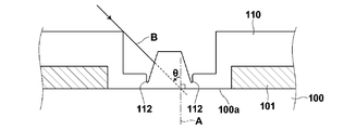
- FIG. 9 is a schematic diagram based on a simulation in the case where vapor deposition is performed using a vapor deposition beam having incident angles of 0 ° and 45 ° with respect to a pixel electrode having a conventional shape whose end is vertically cut. According to this simulation, as shown in FIG. 9, vignetting occurs at the edge of the pixel electrode 101 and the edge of the deposited film itself with respect to the vapor deposition beam having an incident angle of 45 °, and as a result, between the pixel electrodes 101.
- the organic layer 110 had a groove 112 having a wedge-shaped cross section.
- a crack is generated in the organic layer starting from such a groove 112.
- Such a wedge-shaped groove is a problem that arises because it is necessary to form the organic layer at a temperature lower than the glass transition temperature, and does not occur in an image sensor using amorphous selenium described in Patent Document 2. Since amorphous selenium is usually formed at a temperature higher than the glass transition temperature, the surface of the deposited film becomes smooth and almost flat, so that a wedge-shaped groove remains on the surface of the organic layer even if vignetting of the deposition beam occurs. It was because there was nothing.
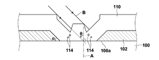
- FIG. 10 is a schematic diagram based on a simulation when the organic layer 110 is formed by vapor deposition with the vapor deposition beam B having incident angles of 0 ° and 45 ° on the pixel electrode 102 having an end portion with an inclination angle of 45 °. . As shown in FIG.
- the present invention has been made in view of the above circumstances, and an object of the present invention is to provide an imaging device that does not cause point defects in an image and a method for manufacturing the imaging device.
- the image sensor of the present invention is an image sensor having a plurality of pixel portions, A plurality of pixel electrodes corresponding to the number of the pixel portions, which are spaced apart from each other on the substrate;
- the pixel electrode has an end inclined at an inclination angle ⁇ (provided that 30 ° ⁇ ⁇ ⁇ 85 °) on the substrate surface of the substrate;
- the organic layer is a film deposited by a deposition beam incident at an incident angle smaller than (90 ° ⁇ max ) with respect to the substrate surface under a deposition substrate temperature condition lower than the glass transition temperature of the organic layer. It is characterized by being.
- ⁇ max is the maximum inclination angle among the inclination angles of the end portions of
- the organic layer is formed along the plurality of pixel electrodes and the recesses between the electrodes, and has the surface of the plurality of pixel electrodes and the recesses between the electrodes almost as they are. Is. Further, the counter electrode formed on the organic layer also has the unevenness of the organic layer on the surface as it is. The surface of the concave portion corresponding to between the pixel electrodes is gentle, and there is no wedge-shaped depression. In addition, since there is almost no cavity near the boundary of the concave portion of the organic layer, there are almost no point defects caused by the cavity near the boundary of the concave portion in the image acquired by the image sensor.
- An image pickup device manufacturing method is an organic image pickup device having a plurality of pixel portions, and includes a plurality of pixel electrodes spaced apart from each other on a substrate, the plurality of pixel electrodes, and between the pixel electrodes.
- a method for producing an organic imaging device comprising: Forming a plurality of pixel electrodes on the substrate as the plurality of electrodes, each having an end inclined at an inclination angle ⁇ (provided that 30 ° ⁇ ⁇ ⁇ 85 °) on the substrate surface of the substrate; On the plurality of pixel electrodes, an organic layer including a photoelectric conversion layer that generates a charge in response to received light is deposited on the substrate surface at a deposition substrate temperature lower than a glass transition temperature of the organic layer. And a vapor deposition film forming step using a vapor deposition beam incident at an incident angle smaller than (90 ° ⁇ max ).
- ⁇ max is the maximum inclination angle among the inclination angles of the end portions of the plurality of pixel electrodes.
- the incident angle of the vapor deposition beam refers to an inclination angle from an axis perpendicular to the substrate surface on which the electrodes are formed.
- the pixel electrode has an end portion inclined at an inclination angle ⁇ x (where 30 ° ⁇ ⁇ ⁇ 85 °) on the substrate surface of the substrate, and is provided on the plurality of pixel electrodes. Since the organic layer is a film formed by vapor deposition with an incident angle smaller than (90 ° - ⁇ max ) with respect to the substrate surface under a vapor deposition substrate temperature condition lower than the glass transition temperature of the organic layer, There are almost no wedge-shaped dents or minute cavities in the portion of the organic layer corresponding to the end of the pixel electrode. Therefore, in the image sensor of the present invention, the occurrence of cracks in the organic layer can be suppressed, and an image free from point defects can be obtained.
- ⁇ x where 30 ° ⁇ ⁇ ⁇ 85 °
- received light is received above a plurality of pixel electrodes having end portions inclined at an inclination angle ⁇ (provided that 30 ° ⁇ ⁇ ⁇ 85 °) on the substrate surface of the substrate. Accordingly, an organic layer including a photoelectric conversion layer that generates electric charge is incident on the substrate surface at an incident angle smaller than (90 ° ⁇ max ) at a temperature lower than the glass transition temperature of the organic layer. And a step of depositing a film with a deposition beam, a minute cavity is not generated in a portion corresponding to between the pixel electrodes of the photoelectric conversion layer, and an image sensor which does not cause point defects can be obtained. In addition, since no wedge-shaped groove or convex portion is formed in the concave portion of the photoelectric conversion layer, generation of cracks can be suppressed, and generation of leakage current does not occur.
- Schematic sectional view showing a part of an image sensor according to an embodiment of the present invention Schematic sectional view showing the inclination angle of the end of the pixel electrode of the image sensor and the incident angle of the vapor deposition beam B of the organic layer
- FIG. 1 is a schematic cross-sectional view showing a configuration of an image sensor 1 according to an embodiment of the present invention.
- the imaging device 1 of the present embodiment is arranged in a continuous film shape on a plurality of pixel electrodes 16 that are spaced apart from each other on a substrate 10 and on and between the plurality of pixel electrodes 16. And an opposing electrode 25 disposed on the organic layer 20.
- Each pixel electrode 16 has an end portion (tapered portion) inclined at an inclination angle ⁇ (provided that 30 ° ⁇ ⁇ ⁇ 85 °) on the substrate surface 10 a of the substrate 10.
- the inclination angle of the end of each pixel electrode 16 is substantially the same, but has some variation.
- the maximum inclination angle among the inclination angles ⁇ of the end portions of all the pixel electrodes 16 is the maximum inclination angle ⁇ max .
- the organic layer 20 includes a photoelectric conversion layer made of an organic photoelectric conversion material that generates charges in response to at least received light, and is composed of one layer or a plurality of layers.
- a charge blocking layer such as an electron blocking layer can be included. Note that a layer made of an inorganic material may be included between the plurality of organic layers.
- the organic layer 20 is a film deposited by a vapor deposition beam incident at an incident angle ⁇ smaller than (90 ° ⁇ max ) with respect to the substrate surface 10a under a vapor deposition substrate temperature condition lower than the glass transition temperature.
- the substrate 10 includes a circuit substrate 11 made of a semiconductor such as glass or silicon, and provided with a circuit including the signal readout unit 17 on the surface, and an insulating layer 12 provided on the surface.
- a circuit substrate 11 made of a semiconductor such as glass or silicon, and provided with a circuit including the signal readout unit 17 on the surface, and an insulating layer 12 provided on the surface.
- the plurality of pixel electrodes 16 are two-dimensionally arranged on the surface of the insulating layer 12 (substrate surface 10a) at regular intervals, and each pixel electrode 16 and the readout unit 17 are electrically connected to the insulating layer 12.
- a connecting portion 18 to be connected to is embedded.
- the connecting portion 18 is a columnar member made of a conductive material such as tungsten (W), and is, for example, a via plug.
- the pixel electrode 16 is a charge collecting electrode for collecting charges generated in the photoelectric conversion layer in the organic layer 20.
- the counter electrode 25 is an electrode facing each pixel electrode 16 and is provided on the organic layer 20.
- the counter electrode 25 applies an electric field to the organic layer 20 by sandwiching the organic layer 20 including the photoelectric conversion layer together with the pixel electrode 16, and collects the charges generated in the photoelectric conversion layer by the pixel electrode 16. Collects charges with the opposite polarity to the signal charge. Since the collection of the reverse polarity charge does not need to be divided among the pixels, the counter electrode 25 can be shared by a plurality of pixels. Therefore, it may be called a common electrode (common electrode).
- the counter electrode 25 is preferably composed of a transparent conductive film in order to allow light to enter the organic layer 20 including the photoelectric conversion layer.
- a metal, a metal oxide, a metal nitride, a metal boride, or an organic conductive material is used. Examples thereof include compounds and mixtures thereof. Specific examples include tin oxide, zinc oxide, indium oxide, indium tin oxide (ITO), indium zinc oxide (IZO), indium tungsten oxide (IWO), conductive metal oxides such as titanium oxide, and metal nitrides such as TiN.
- ITO Indium Tin Oxide
- Pt platinum
- silver Ag
- Cr chromium
- Ni nickel
- Al aluminum
- ITO inorganic conductive compounds
- tin oxide antimony-doped tin oxide
- FTO fluorine-doped tin oxide
- ZO gallium-doped zinc oxide
- the surface resistance of the counter electrode 25 is preferably 10 k ⁇ / ⁇ or less, more preferably 1 k ⁇ / ⁇ or less when the signal reading unit 17 is a CMOS type.
- the signal reading unit 17 is a CCD type, it is preferably 1 k ⁇ / ⁇ or less, more preferably 0.1 k ⁇ / ⁇ or less.
- one photoelectric conversion element is constituted by one pixel electrode 16, the counter electrode 25 thereabove, and the organic layer 20 disposed between these electrodes.
- the signal readout unit 17 is provided corresponding to each of the plurality of pixel electrodes 16 and outputs a signal corresponding to the charge collected by the corresponding pixel electrode 16.
- the signal reading unit 17 is configured by, for example, a CCD, a MOS transistor circuit (MOS circuit), a TFT circuit, or the like.
- the signal reading unit 17 when the signal reading unit 17 is a MOS circuit, the signal reading unit 17 includes a floating diffusion, a reset transistor, an output transistor, and a selection transistor (not shown).
- the reset transistor, the output transistor, and the selection transistor are each configured by an n-channel MOS transistor (hereinafter referred to as an nMOS transistor).
- the signal readout unit 17 reads out a signal corresponding to the charge collected by the pixel electrode 16 with such a circuit configuration.
- one pixel unit 30 (a portion surrounded by a broken line in FIG. 1) is composed of one photoelectric conversion element and the corresponding signal readout unit 17. That is, the imaging device 1 has a plurality of pixel units 30 arranged in an array.
- each pixel electrode 16 becomes a signal at the signal reading unit 17 of each corresponding pixel unit 30, and an image is synthesized based on the signals acquired from the plurality of pixel units.
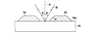
- 2 and 3 are schematic cross-sectional views showing the inclination angle ⁇ of the pixel electrode 16 and the incident angle ⁇ of the vapor deposition beam of the organic layer 20.
- the plurality of pixel electrodes 16 are formed on the insulating layer 12 (substrate surface 10a) by sputtering or the like and then etched through a mask to form a predetermined pattern before the organic layer 20 is formed. In FIG. 2, the substrate surface 10a is exposed between the pixel electrodes 16 (see FIG. 2).
- the pixel electrode is not particularly limited as long as it is a conductive material generally used as an electrode, but tungsten (W), TiN, or the like can be preferably used.
- the size of the pixel electrode 16 is preferably 3 ⁇ m or less because the effect of the present invention is remarkable. More preferably, it is 2 ⁇ m or less. More preferably, it is 1.5 ⁇ m or less.
- the gap between the pixel electrodes 16 is preferably 0.3 ⁇ m or less because the effect of the present invention is remarkable, more preferably 0.25 ⁇ m or less, and still more preferably 0.2 ⁇ m or less.
- the inclination angle ⁇ of the end portion of the pixel electrode is an angle formed by the substrate surface 10a and the end portion of the pixel electrode.
- the inclination angle ⁇ of the pixel electrode is set to 30 ° or more and 85 ° or less. Although it is desirable for the plurality of pixel electrodes formed in one image sensor to have substantially the same inclination angle, there may be variations within a range of 30 ° to 85 °. A more preferable inclination angle is 45 ° or more and 75 ° or less.
- the inclination angle ⁇ is smaller, the occurrence of defects in the organic layer provided thereon is suppressed. However, when it is less than 30 °, afterimage generation may occur, which is not preferable.
- the electric field generated when the inclined end portion is charged acts on the region above the gap between the pixel electrodes, and the region above the gap between the pixel electrodes is reduced. Since it is easy to draw the leaked charge that has passed through the inclined electrode surface, it is possible to reduce the occurrence of an afterimage due to the leaked charge.
- the organic layer 20 is formed so as to cover the substrate surface 10 a exposed between the plurality of pixel electrodes 16 and the pixel electrodes 16.
- the organic layer 20 is formed by vapor deposition, and the shape between the pixel electrode, the electrode end portion, and the pixel electrode is reflected on the surface thereof.
- the incident angle ⁇ of the vapor deposition beam B for forming the organic layer 20 is an inclination angle of the vapor deposition beam with respect to the axis A perpendicular to the substrate surface 10a.
- the relationship between the organic layer 20 and the maximum inclination angle ⁇ max among the inclination angles ⁇ of the plurality of pixel electrodes is ⁇ ⁇ (90 ° ⁇ max ) with respect to the substrate 10 on which the plurality of pixel electrodes are formed.
- the film is formed by a vapor deposition beam having an incident angle ⁇ .
- the incident angle range satisfying ⁇ ⁇ (90 ° ⁇ max ) is shown in a conical shape. In vapor deposition, only a single incident angle vapor deposition beam may be used. However, as long as this ⁇ ⁇ (90 ° ⁇ max ) is satisfied, a vapor beam including various incident angles may be used.
- the vapor deposition beam having such an incident angle ⁇ is irradiated on the pixel electrode and the substrate surface exposed between the pixel electrodes without being vignetted by the organic layer 20 to be formed. Therefore, the organic layer 20 along the shape of the pixel electrode 16 can be deposited on the organic layer 20 without forming the wedge-shaped groove 112 and the cavity 114 as shown in FIG. 9 or FIG.
- the organic layer 20 includes at least a photoelectric conversion layer, and may include a charge blocking layer and the like.
- the charge blocking layer has a function of suppressing dark current.
- the charge blocking layer may be composed of a plurality of layers, for example, may be composed of a first blocking layer and a second blocking layer. As described above, by forming the charge blocking layer into a plurality of layers, an interface is formed between the first blocking layer and the second blocking layer, and discontinuity occurs in the intermediate level existing in each layer, so that It becomes difficult for the charge carrier to move through the level, and dark current can be suppressed.
- the charge blocking layer may be a single layer.
- the photoelectric conversion layer includes a p-type organic semiconductor and an n-type organic semiconductor.
- Exciton dissociation efficiency can be increased by joining a p-type organic semiconductor and an n-type organic semiconductor to form a donor-acceptor interface. For this reason, the photoelectric conversion layer of the structure which joined the p-type organic semiconductor and the n-type organic semiconductor expresses high photoelectric conversion efficiency.
- a photoelectric conversion layer in which a p-type organic semiconductor and an n-type organic semiconductor are mixed is preferable because the junction interface is increased and the photoelectric conversion efficiency is improved.
- a p-type organic semiconductor is a donor organic semiconductor, and is mainly represented by a hole-transporting organic compound and means an organic compound having a property of easily donating electrons. More specifically, an organic compound having a smaller ionization potential when two organic materials are used in contact with each other. Therefore, any organic compound can be used as the donor organic compound as long as it is an electron-donating organic compound.
- the metal complex etc. which it has as can be used.
- any organic compound having an ionization potential smaller than that of an organic compound used as an n-type (acceptor) compound may be used as a donor organic semiconductor.
- An n-type organic semiconductor is an acceptor organic semiconductor, and is mainly represented by an electron-transporting organic compound and refers to an organic compound having a property of easily accepting electrons. More specifically, an n-type organic semiconductor refers to an organic compound having a higher electron affinity when two organic compounds are used in contact with each other. Therefore, any organic compound can be used as the acceptor organic compound as long as it is an electron-accepting organic compound.
- condensed aromatic carbocyclic compounds naphthalene derivatives, anthracene derivatives, phenanthrene derivatives, tetracene derivatives, pyrene derivatives, perylene derivatives, fluoranthene derivatives
- 5- to 7-membered heterocyclic compounds containing nitrogen atoms, oxygen atoms, and sulfur atoms E.g., pyridine, pyrazine, pyrimidine, pyridazine, triazine, quinoline, quinoxaline, quinazoline, phthalazine, cinnoline, isoquinoline, pteridine, acridine, phenazine, phenanthroline, tetrazole, pyrazole, imidazole, thiazole, oxazole, indazole, benzimidazole, benzotriazole, Benzoxazole, benzothiazole, carbazole, purine, triazolopyrid
- Any organic dye may be used as the p-type organic semiconductor or the n-type organic semiconductor, but preferably a cyanine dye, a styryl dye, a hemicyanine dye, a merocyanine dye (including zero methine merocyanine (simple merocyanine)), 3 Nuclear merocyanine dye, 4-nuclear merocyanine dye, rhodacyanine dye, complex cyanine dye, complex merocyanine dye, allopolar dye, oxonol dye, hemioxonol dye, squalium dye, croconium dye, azamethine dye, coumarin dye, arylidene dye, anthraquinone dye, tri Phenylmethane dye, azo dye, azomethine dye, spiro compound, metallocene dye, fluorenone dye, fulgide dye, perylene dye, perinone dye, phenazine dye, pheno
- fullerene or a fullerene derivative having excellent electron transport properties.
- Fullerenes are fullerene C 60 , fullerene C 70 , fullerene C 76 , fullerene C 78 , fullerene C 80 , fullerene C 82 , fullerene C 84 , fullerene C 90 , fullerene C 96 , fullerene C 240 , fullerene 540 , mixed fullerene Represents a fullerene nanotube, and a fullerene derivative represents a compound having a substituent added thereto.
- the substituent for the fullerene derivative is preferably an alkyl group, an aryl group, or a heterocyclic group.
- the alkyl group is more preferably an alkyl group having 1 to 12 carbon atoms, and the aryl group and the heterocyclic group are preferably benzene ring, naphthalene ring, anthracene ring, phenanthrene ring, fluorene ring, triphenylene ring, naphthacene ring.
- substituents may further have a substituent, and the substituents may be bonded as much as possible to form a ring.
- substituents may be bonded as much as possible to form a ring.
- you may have a some substituent and they may be the same or different.
- a plurality of substituents may be combined as much as possible to form a ring.
- the photoelectric conversion layer contains fullerene or a fullerene derivative
- electrons generated by photoelectric conversion can be quickly transported to the pixel electrode 16 or the counter electrode 25 via the fullerene molecule or the fullerene derivative molecule.
- fullerene molecules or fullerene derivative molecules are connected to form an electron path, the electron transport property is improved, and the high-speed response of the photoelectric conversion element can be realized.
- the p-type organic semiconductor is reduced, the junction interface is reduced, and the exciton dissociation efficiency is lowered.
- a triarylamine compound described in Japanese Patent No. 4213832 is used as a p-type organic semiconductor mixed with fullerene or a fullerene derivative in a photoelectric conversion layer
- a high SN ratio of the photoelectric conversion element can be expressed. preferable. If the ratio of fullerene or fullerene derivative in the photoelectric conversion layer is too large, the amount of the triarylamine compound is reduced and the amount of incident light absorbed is reduced. As a result, the photoelectric conversion efficiency is reduced, so that the fullerene or fullerene derivative contained in the photoelectric conversion layer preferably has a composition of 85% or less.
- An electron donating organic material can be used for the first blocking layer and the second blocking layer.
- Polyphyrin compounds triazole derivatives, oxa Use of zazole derivatives, imidazole derivatives, polyarylalkane derivatives, pyrazoline derivatives, pyrazolone derivatives, phenylenediamine derivatives, annealed amine derivatives, amino-substituted chalcone derivatives, oxazole derivatives, styrylanthracene derivatives, fluorenone derivatives, hydrazone derivatives, silazane derivatives, etc.
- a polymer such as phenylene vinylene, fluorene, carbazole, indole, pyrene, pyrrole, picoline, thiophene, acetylene, diacetylene, or a derivative thereof can be used. Any compound having sufficient hole transportability can be used.
- An inorganic material can also be used as the charge blocking layer.
- an inorganic material has a dielectric constant larger than that of an organic material, when used in a charge blocking layer, a large voltage is applied to the photoelectric conversion layer, and the photoelectric conversion efficiency can be increased.
- Materials that can be a charge blocking layer include calcium oxide, chromium oxide, chromium oxide copper, manganese oxide, cobalt oxide, nickel oxide, copper oxide, gallium copper oxide, strontium copper oxide, niobium oxide, molybdenum oxide, indium copper oxide, oxide Examples include indium silver and iridium oxide.
- the layer adjacent to the photoelectric conversion layer among the plurality of layers is preferably a layer made of the same material as the p-type organic semiconductor contained in the photoelectric conversion layer. In this way, by using the same p-type organic semiconductor for the charge blocking layer, it is possible to suppress the formation of an intermediate level at the interface between the photoelectric conversion layer and the adjacent layer, and to further suppress the dark current. .
- the layer can be a layer made of an inorganic material, or in the case of a plurality of layers, one or more layers can be a layer made of an inorganic material. .
- the signal readout unit 17 is formed on a substrate such as silicon to manufacture the circuit board 11. Thereafter, an insulating layer 12 is formed on the light incident side surface of the circuit board 11, and the surface of the insulating layer 12 is polished and planarized by CMP or the like. Then, a hole for forming the connection portion 18 is formed in the insulating layer 12 by a photolithography process and a dry etching process. The hole is formed in a portion of the insulating layer 12 positioned below the region where the pixel electrode 16 is formed. The connecting portion 18 is formed in the formed hole using a conductive material.
- the semiconductor circuit board 11 including the insulating layer 12 and the connection portion 18 embedded in the insulating layer 12 is a substrate 10
- the surface of the insulating layer 12 is a substrate surface 10 a.
- the pixel electrode 16 is formed by depositing the material of the pixel electrode 16 on the insulating layer 12 by a physical vapor deposition (PVD) method and patterning the deposited film.
- PVD physical vapor deposition
- a physical vapor deposition method for example, a sputtering method is used.
- patterning is performed so that a plurality of pixel electrodes 16 are arranged on the surface of the insulating layer 12 at regular intervals. At this time, the etching is performed so that the end portion of the pixel electrode 16 has a desired inclination angle ⁇ (30 ° ⁇ ⁇ ⁇ 85 °).
- a tapered portion having a desired inclination angle ⁇ can be formed at the end portion of the pixel electrode. Details of the method for forming the tapered portion are described in, for example, Japanese Patent Application Laid-Open No. 2011-35418.
- a plurality of pixel electrodes 16 are formed on the substrate surface 10a of the substrate 10 as shown in FIG. At this time, the plurality of pixel electrodes 16 are two-dimensionally arranged apart from each other, and the substrate surface 10 a is exposed between the pixel electrodes 16.
- the organic layer 20 is deposited so as to cover the plurality of pixel electrodes 16 and the substrate surface 10a therebetween.
- a vacuum vapor deposition method is used for the vapor deposition of the organic layer 20. More specifically, a resistance heating evaporation method or an electron beam heating evaporation method is used.
- the vapor deposition of the organic layer 20 is performed in a state where the vapor deposition substrate temperature is lower than the glass transition temperature of the organic layer 20.
- the glass transition temperature can be measured by, for example, DSC (differential scanning calorimetry).
- the relationship between the inclination angle ⁇ of the plurality of pixel electrodes and the maximum inclination angle ⁇ max is an incident angle ⁇ where ⁇ ⁇ (90 ° ⁇ max ).
- the organic layer 20 is deposited on the pixel electrode 16 and the substrate surface 10a exposed between the pixel electrodes by irradiating the deposition beam.
- the organic layer 20 along the shape of the pixel electrode 16 can be deposited without forming the wedge-shaped groove 112 and the cavity 114 as shown in FIG. 9 or FIG.
- the incident angle of the vapor deposition beam B can be controlled for each pixel electrode, the incident angle ⁇ of the vapor deposition beam B should be smaller than 90 ° ⁇ with respect to the inclination angle ⁇ of the end of each pixel electrode. Since it is difficult to control the incident angle ⁇ of the vapor deposition beam B for each individual pixel electrode, the maximum inclination angle ⁇ max is defined here.
- the incident angle ⁇ of the vapor deposition beam may be ⁇ ⁇ 90 ° ⁇ max , but considering errors in the vapor deposition apparatus, ⁇ ⁇ 90 ° ⁇ ( ⁇ max + 2 °), and further ⁇ ⁇ 90 °. ⁇ ( ⁇ max + 5 °) is preferable.
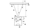
- FIG. 4 is a perspective view schematically showing an organic layer deposition method on a substrate. As shown in FIG. 4, the organic layer is deposited in a state where the substrate 10 is disposed above the opening of the deposition cell 40.
- the vapor deposition cell 40 includes a first opening 42, a cylindrical accommodating portion 41 that stores the vapor deposition raw material 60 therein, and a second opening 44 that is formed continuously with the accommodating portion 41 and surrounds the first opening 42. And a cylindrical portion 45 provided with
- the emission angle of the vapor deposition beam B can be adjusted by adjusting the opening diameters of the first opening 42 and the second opening 44. As shown in FIG. 4, the deposition material spreads in a substantially conical shape from the opening 44 of the deposition cell 40 toward the substrate 10.
- FIG. 5 is a cross-sectional view schematically showing the positional relationship between the substrate 10 and the vapor deposition cell 40.
- the spread angle ⁇ of the vapor deposition beam B can be defined by the opening diameter d1 of the first opening 42, the opening diameter d2 of the second opening 44, and the distance L between the openings 42 and 44,
- the spread angle ⁇ is the inclination from the axis A perpendicular to the substrate surface 10a, that is, the maximum incident angle ⁇ of the vapor deposition beam B with respect to the substrate surface 10a.
- the vapor deposition beam from the vapor deposition cell 40 is incident on the substrate surface 10a at an incident angle of 0 ° to ⁇ .
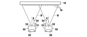
- FIG. 6 is a cross-sectional view schematically showing another organic layer deposition method.
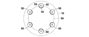
- the organic layer 20 may be deposited by disposing the substrate 10 above the plurality of deposition cells 50.
- the vapor deposition cell 50 includes an opening 52, and includes a cylindrical accommodating portion 51 that stores the vapor deposition raw material 60 therein, and a wall portion 54 that is erected on a part of the upper surface having the opening 52 of the accommodating portion 51.
- the wall part 54 is provided in the part which becomes the center part side of the board
- the wall portion 54 can define the incident angle ⁇ of the vapor deposition beam at least on the central portion side of the substrate 10.
- the incident angle ⁇ is smaller than 90 ° ⁇ max with respect to the outer peripheral side of the substrate 10.
- the vapor deposition beam larger than ° - ⁇ max may be set so as not to enter the substrate surface (including the pixel electrode).
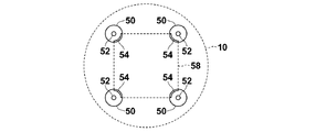
- the deposition cell 50 is disposed at positions corresponding to the four corners of a square 58 smaller than the substrate 10 with respect to the disc-shaped substrate 10, or as compared with the disc-shaped substrate 10 as shown in FIG. 8.
- a method of arranging a plurality on the small concentric circles 59 is preferable.
- the wall portion 54 of the vapor deposition cell 50 only needs to be erected at least in the entire area inside the square 58.
- the wall portion 54 of the vapor deposition cell 50 only needs to be erected at least on the entire inner side of the concentric circle 59.
- the examples and comparative examples were produced based on the following conditions.
- the configuration is as shown in FIG. 1, but the inclination angle of the end of the pixel electrode and the conditions of the vapor deposition beam of the organic layer are different for each example and comparative example.
- the production methods of Examples and Comparative Examples are as follows.
- a pixel electrode 16 having an end portion with an inclination angle ⁇ was formed on a substrate 10 including a circuit manufactured by a standard CMOS image sensor process.
- the pixel size was 3 ⁇ m.
- Tungsten (W) was used as the material of the pixel electrode 16.
- a tungsten film is formed on the substrate surface 10a of the substrate 10 by sputtering, and then a resist mask is formed by lithography, and the tungsten film is selectively etched.
- a dry etching apparatus Model E645-ICP Matsushita Electric Industrial Co., Ltd.
- ICP inductively coupled plasma
- Table 1 shows the maximum inclination angle ⁇ max (°) and the conditions for realizing the inclination angle.
- an electron blocking layer is formed at a deposition rate of 10 to 12 nm / s at a deposition rate of 10 to 12 nm / s on the pixel electrode while rotating a holder for holding the substrate in a deposition chamber whose pressure is reduced to 1 ⁇ 10 ⁇ 4 Pa or less. It vapor-deposited so that it might become.
- the volume ratio of the chemical formula 1 and the chemical formula 2 becomes 1: 3 at the deposition rates of 16 to 18 nm / s and 25 to 28 nm / s for the material shown by the chemical formula 1 (fullerene 60) and the material shown by the chemical formula 2, respectively.
- a photoelectric conversion layer was formed by co-evaporation. The thickness was 400 nm.
- the organic vapor deposition cell 40 having the shape shown in FIGS. 4 and 5 was used, and the conditions of the incident beam at the time of forming the organic layer were as follows.
- Table 2 shows the maximum incident angle ⁇ of the vapor deposition beam and the conditions for realizing the incident angle.
- the film was transferred to a sputtering chamber, and an ITO film as a counter electrode was formed to a thickness of 10 nm on the photoelectric conversion layer by RF magnetron sputtering.
- Examples 1 to 5 and Comparative Examples 1 to 5 were fabricated by various combinations of the pixel electrode manufacturing conditions shown in Table 1 and the organic layer deposition conditions shown in Table 2.
- Table 3 shows the results of evaluating the maximum inclination angle ⁇ max of the pixel electrode, the incident angle ⁇ of the vapor deposition beam, and the presence or absence of cracks and bites (grooves, cavities) in the organic layer for Examples 1 to 5 and Comparative Examples 1 to 5. .
- Example 1 In Example 1, a pixel electrode was formed under a pixel electrode production condition II with a pixel electrode end maximum inclination angle of 85 ° ( ⁇ max ), and an organic layer was deposited under a vapor deposition condition A with a vapor deposition beam angle of 4 ° ( ⁇ ). .
- Example 2 In Example 2, the pixel electrode was formed under the pixel electrode manufacturing condition III with the pixel electrode end maximum tilt angle of 70 °, and the organic layer was deposited under the deposition condition B with the deposition beam angle of 13 °.
- Example 3 the pixel electrode was formed under the pixel electrode manufacturing condition IV having a maximum tilt angle of 60 ° at the end of the pixel electrode, and the organic layer was deposited under the deposition condition D at the deposition beam angle of 29 °.
- Example 4 the pixel electrode was formed under the pixel electrode manufacturing condition V with the pixel electrode end maximum inclination angle of 45 °, and the organic layer was deposited under the deposition condition F with the deposition beam angle of 41 °.
- Example 5 the pixel electrode was formed under the pixel electrode manufacturing condition VI having a maximum inclination angle of 30 ° at the end of the pixel electrode, and the organic layer was deposited under the deposition condition G at the deposition beam angle of 46 °.
- Comparative Example 1 In Comparative Example 1, the pixel electrode was formed under the pixel electrode manufacturing condition I with a maximum tilt angle of 90 ° at the end of the pixel electrode, and the organic layer was deposited under the deposition condition A with a deposition beam angle of 4 °.
- Comparative Example 2 In Comparative Example 2, the pixel electrode was formed under the pixel electrode production condition II with a maximum inclination angle of 85 ° of the pixel electrode, and the organic layer was deposited under the deposition condition C with the deposition beam angle of 21 °.
- Comparative Example 3 In Comparative Example 3, the pixel electrode was formed under the condition of pixel electrode manufacturing condition III having a maximum tilt angle of 70 ° at the end of the pixel electrode, and the organic layer was deposited under the deposition condition E at the deposition beam angle of 35 °.
- Comparative Example 4 In Comparative Example 4, the pixel electrode was formed under the pixel electrode manufacturing condition V with the pixel electrode end maximum inclination angle of 45 °, and the organic layer was deposited under the deposition condition G with the deposition beam angle of 46 °.
- Comparative Example 5 (Comparative Example 5)
- the pixel electrode was formed under the pixel electrode manufacturing condition VI having a maximum inclination angle of 30 ° at the end of the pixel electrode, and the organic layer was deposited under the deposition condition J at the deposition beam angle of 61 °.
- Examples 1-5 both are those 30 ° ⁇ ⁇ ⁇ 85 ° cutlet theta satisfies the condition ⁇ 90 ° - ⁇ max, Comparative Examples 1 to 5, 30 ° ⁇ ⁇ ⁇ 85 ° cutlet theta ⁇ 90 The condition of ° - ⁇ max is not satisfied.
- Table 3 shows the maximum inclination angle ⁇ max and the maximum incident angle ⁇ of the vapor deposition beam of each example and comparative example, and also shows the presence or absence of cracks and bites.
Landscapes
- Physics & Mathematics (AREA)
- Electromagnetism (AREA)
- Solid State Image Pick-Up Elements (AREA)
- Light Receiving Elements (AREA)
Abstract
【課題】画像に点欠陥を生じない撮像素子を得る。 【解決手段】画素電極(16)は、基板(10)の基板面(10a)に傾斜角度α(但し、30°≦α≦85°)で傾斜する端部を有するものとし、この画素電極(16)上に設けられる有機層(20)は、その有機層(20)のガラス転移温度より低い蒸着基板温度条件下で基板面(10a)に対して(90°-αmax)より小さい入射角θで入射する蒸着ビームBにより蒸着してされてなるものとする。ここで、αmaxは、複数の画素電極の端部の傾斜角度のうち最大の傾斜角度である。
Description
本発明は撮像素子に関するものであり、特に、画素部に有機層からなる光電変換層を有する有機光電変換素子を備えてなる撮像素子に関するものである。
デジタルスチルカメラ、デジタルビデオカメラ、携帯電話用カメラ、内視鏡用カメラ等に利用されているイメージセンサとして、CCDセンサやCMOSセンサなどの撮像素子が広く知られている。
現在、読出し回路等が形成された基板上に複数の画素電極が二次元状に配列形成され、その上に少なくとも光電変換層を含む有機層、対向電極が順次設けられてなる積層型の撮像素子が提案されている(特許文献1)。
特許文献1に記載の積層型の撮像素子においては、光電変換層は、全画素部に共通に一枚構成としてもよいし、画素部毎に分割されていてもよい。
一方で、複数の画素電極上に共通膜状に光電変換層が設けられた構成の撮像素子においては、画素電極間に残留電荷が帯電し、画像情報の残像として残ってしまう、画素電極の端部上の光電変換層の厚みが薄くなると共に電界集中が起こりリーク電流が発生するなどの問題がある。特許文献2、3等においては、このような問題を解決するために、画素電極の端部を傾斜させたものとすることが提案されている。特許文献2では、画素電極間に帯電する電荷による残像の発生を抑制するために、画素電極の端部を平面基板に対して30°~120°の範囲で傾斜するように構成することが好ましい旨が記載されている。特許文献3には、画素電極端部の段差部で光電変換層の厚みが薄くなったり、電界集中が発生するのを抑制するため、90°よりも小さい所定の傾斜角度で傾斜するように構成することが好ましいことが記載されている。
有機光電変換層を複数の画素部に共通膜として備えた撮像素子においても、残像を抑制するため、あるいは電荷集中等の抑制するために、画素電極の端部を基板面に対して傾斜させて形成することが考えられる。
しかしながら、本発明者らが画素電極端部に傾斜を設けてその上に有機光電変換層を蒸着形成した撮像素子を作製したところ、そのような撮像素子で取得した画像には点欠陥が多数生じる場合があることが分かった。
本発明者らは、有機光電変換層を備えた撮像素子独自の問題点をシミュレーションを行い明確にした。
蒸着の際には、基板の蒸着面に対向して蒸着源(蒸着セル)が配置されており、蒸着面には様々な入射角で蒸着ビームが入射してくる。図9は、端部が垂直に切り立った従来形状の画素電極に対し、0°および45°の入射角の蒸着ビームを用いて蒸着させた場合のシミュレーションに基づく模式図である。このシミュレーションによると、図9に示すように、45°の入射角の蒸着ビームについては画素電極101の端部および蒸着された膜自体の端部によるケラレが生じ、結果として、画素電極101間において有機層110に断面楔形の溝112が生じていることがわかった。そして、実際に従来の端部が垂直な画素電極上に蒸着により有機層を形成した撮像素子においては、このような溝112の部分を起点として有機層にクラックが生じていた。
このような楔形の溝は、有機層をガラス転移温度以下の温度で形成する必要があることから生じる問題であり、特許文献2に記載のアモルファスセレンを用いた撮像素子においては生じない。通常アモルファスセレンはガラス転移温度より高温で形成するため、成膜された膜表面がなだらかになりほぼ平坦なものとなるため、蒸着ビームのケラレが生じても楔形の溝が有機層の表面に残ることはなかったためである。
一方で、上述の通り、特許文献2、3のように画素電極を端部に傾斜を有するものとすれば、上述のような楔型の溝は生じないものと予想される。また、蒸着時に端部の傾斜角度と同じだけ基板面に対して傾いた蒸着ビームであれば、ケラレが生じないと予想される。
しかしながら、予想に反し、蒸着時に端部の傾斜角度と同じ角度基板面に対して傾いた蒸着ビームを用いた場合にもケラレが生じていることが明らかになった。図10は、傾斜角度が45°の端部を有する画素電極102上に0°および45°の入射角を有する蒸着ビームBで有機層110を蒸着形成させた場合のシミュレーションに基づく模式図である。図10に示すように、基板面100aに対しα=45°の傾斜角度を有する画素電極102に対し、入射角θ=45°の蒸着ビームBを用いて有機層110を成膜すると、膜の成長に伴い、蒸着ビームBの一部にケラレが発生することが分かった。このケラレにより画素電極102の端部と画素間との境界部分の有機層110中に小さな空洞114が複数形成されている。本発明者らは、この空洞114が点欠陥の主なる原因であることを見出だした。
本発明は上記事情に鑑みてなされたものであって、画像に点欠陥を生じない撮像素子およびその撮像素子の製造方法を提供することを目的とするものである。
本発明の撮像素子は、複数の画素部を有する撮像素子であって、
基板上に互いに離間して配された、前記画素部の数に対応する複数の画素電極と、
該複数の画素電極上および該画素電極間に連続膜状に配された、前記複数の画素部に共有される、光電変換層を含む有機層と、
該有機層の上に配された、前記複数の画素部に共有される対向電極とを含み、
前記画素電極が、前記基板の基板面に傾斜角度α(但し、30°≦α≦85°)で傾斜する端部を有し、
前記有機層が、該有機層のガラス転移温度より低い蒸着基板温度条件下で前記基板面に対して、(90°-αmax)より小さい入射角で入射する蒸着ビームにより蒸着されてなる膜であることを特徴とするものである。ここで、αmaxは、前記複数の画素電極の端部の傾斜角度のうち最大の傾斜角度である。
基板上に互いに離間して配された、前記画素部の数に対応する複数の画素電極と、
該複数の画素電極上および該画素電極間に連続膜状に配された、前記複数の画素部に共有される、光電変換層を含む有機層と、
該有機層の上に配された、前記複数の画素部に共有される対向電極とを含み、
前記画素電極が、前記基板の基板面に傾斜角度α(但し、30°≦α≦85°)で傾斜する端部を有し、
前記有機層が、該有機層のガラス転移温度より低い蒸着基板温度条件下で前記基板面に対して、(90°-αmax)より小さい入射角で入射する蒸着ビームにより蒸着されてなる膜であることを特徴とするものである。ここで、αmaxは、前記複数の画素電極の端部の傾斜角度のうち最大の傾斜角度である。
本発明の撮像素子は、その有機層は前記複数の画素電極およびその電極間となる凹部に沿って形成され、複数の画素電極の表面とその電極間の凹部からなる凹凸をほぼそのまま表面に有するものである。またその有機層上に形成されている対向電極も有機層の凹凸をほぼそのまま表面に有するものである。画素電極間に対応する凹部の表面はなだらかであり楔形の窪みは存在しない。また、有機層の凹部の境界付近に空洞がほとんど存在しないため、撮像素子で取得される画像に凹部の境界付近の空洞により生じる点欠陥はほとんど存在しない。
本発明の撮像素子の製造方法は、複数の画素部を有する有機撮像素子であって、基板上に互いに離間して配置された複数の画素電極と、該複数の画素電極上および該画素電極間に連続膜状に配置された、前記複数の画素部に共有される、光電変換層を含む有機層と、該有機層の上に配置された、前記複数の画素部に共有される対向電極とを含む有機撮像素子の製造方法であって、
前記基板上に、前記複数の電極として、該基板の基板面に傾斜角度α(但し、30°≦α≦85°)で傾斜する端部を有する画素電極を複数形成する工程と、
該複数の画素電極の上に、受光した光に応じて電荷を生成する光電変換層を含む有機層を、蒸着基板温度が該有機層のガラス転移温度より低い温度で、前記基板面に対して(90°-αmax)より小さい入射角で入射する蒸着ビームにより蒸着成膜する工程とを含むことを特徴とするものである。ここで、αmaxは、前記複数の画素電極の端部の傾斜角度のうち最大の傾斜角度である。
前記基板上に、前記複数の電極として、該基板の基板面に傾斜角度α(但し、30°≦α≦85°)で傾斜する端部を有する画素電極を複数形成する工程と、
該複数の画素電極の上に、受光した光に応じて電荷を生成する光電変換層を含む有機層を、蒸着基板温度が該有機層のガラス転移温度より低い温度で、前記基板面に対して(90°-αmax)より小さい入射角で入射する蒸着ビームにより蒸着成膜する工程とを含むことを特徴とするものである。ここで、αmaxは、前記複数の画素電極の端部の傾斜角度のうち最大の傾斜角度である。
本発明において、蒸着ビームの入射角とは、電極が形成されている基板面に垂直な軸からの傾き角をいう。
本発明の撮像素子は、画素電極が、基板の基板面に傾斜角度αx(但し、30°≦α≦85°)で傾斜する端部を有しており、複数の画素電極上に設けられる有機層が、有機層のガラス転移温度より低い蒸着基板温度条件下で前記基板面に対して(90°-αmax)より小さい入射角で入射する蒸着ビームにより蒸着されてなる膜であるため、有機層の画素電極端部に対応する部分に楔形の微小な窪みや微小な空洞がほとんどない。そのため、本発明の撮像素子においては、有機層でのクラックの発生を抑制することができ、また、点欠陥のない画像を得ることができる。
本発明の撮像素子の製造方法によれば、基板の基板面に傾斜角度α(但し、30°≦α≦85°)で傾斜する端部を有する複数の画素電極の上方に、受光した光に応じて電荷を生成する光電変換層を含む有機層を、蒸着基板温度が該有機層のガラス転移温度より低い温度で、基板面に対して(90°-αmax)より小さい入射角で入射する蒸着ビームにより蒸着成膜する工程とを含むので、光電変換層の画素電極間に相当する部分に微小な空洞部が発生することがなく、点欠陥を生じない撮像素子を得ることができる。
また、光電変換層の凹部に楔型の溝や凸部も生じないため、クラックの発生も抑制することができ、リーク電流の発生などが生じない。
また、光電変換層の凹部に楔型の溝や凸部も生じないため、クラックの発生も抑制することができ、リーク電流の発生などが生じない。
本発明の実施の形態を図面を参照して説明する。
「撮像素子」
図1は、本発明の実施形態にかかる撮像素子1の構成を示す断面模式図である。
図1に示すように、本実施形態の撮像素子1は、基板10上に互いに離間して配された複数の画素電極16と、複数の画素電極16上および画素電極間に連続膜状に配された有機層20と、有機層20の上に配された対向電極25とを備えている。
図1は、本発明の実施形態にかかる撮像素子1の構成を示す断面模式図である。
図1に示すように、本実施形態の撮像素子1は、基板10上に互いに離間して配された複数の画素電極16と、複数の画素電極16上および画素電極間に連続膜状に配された有機層20と、有機層20の上に配された対向電極25とを備えている。
それぞれの画素電極16は、基板10の基板面10aに傾斜角度α(但し、30°≦α≦85°)で傾斜する端部(テーパ部)を有している。各画素電極16の端部の傾斜角度は、ほぼ同様であるが、多少のばらつきを有している。なお、全画素電極16の端部の傾斜角度αのうちの最大の傾斜角度が最大傾斜角度αmaxである。
有機層20は、少なくとも受光した光に応じて電荷を発生する有機の光電変換材料からなる光電変換層を含むものであり、一層もしくは複数層から構成される。光電変換層の他に電子ブロッキング層などの電荷ブロッキング層を含むことができる。なお、複数の有機層間には、無機材料からなる層が含まれていてもよい。
有機層20は、ガラス転移温度より低い蒸着基板温度条件下で基板面10aに対して(90°-αmax)より小さい入射角θで入射する蒸着ビームにより蒸着されてなる膜である。
基板10は、ガラスまたはシリコン等の半導体からなる、表面に信号読出し部17を含む回路を備えた回路基板11と、その表面に設けられた絶縁層12とを含んでいる。
複数の画素電極16は、絶縁層12表面(基板面10a)に二次元状に、一定の間隔をあけて配列されており、絶縁層12には、各画素電極16と読出し部17を電気的に接続する接続部18が埋設されている。接続部18は、タングステン(W)等の導電性材料からなる柱状の部材であって、例えばビアプラグである。
画素電極16は、有機層20内の光電変換層で発生した電荷を捕集するための電荷捕集用の電極である。
対向電極25は各画素電極16と対向する電極であり、有機層20上に設けられている。
対向電極25は、光電変換層を含む有機層20を、画素電極16と共に挟込むことで有機層20に電界を掛け、又、光電変換層で発生した電荷のうち、画素電極16で捕集する信号電荷と逆の極性を持つ電荷を捕集する。この逆極性電荷の捕集は各画素間で分割する必要がないため、対向電極25は複数の画素で共通にすることができる。そのために共通電極(コモン電極)と呼ばれることもある。
対向電極25は、光電変換層を含む有機層20を、画素電極16と共に挟込むことで有機層20に電界を掛け、又、光電変換層で発生した電荷のうち、画素電極16で捕集する信号電荷と逆の極性を持つ電荷を捕集する。この逆極性電荷の捕集は各画素間で分割する必要がないため、対向電極25は複数の画素で共通にすることができる。そのために共通電極(コモン電極)と呼ばれることもある。
対向電極25は、光電変換層を含む有機層20に光を入射させるため、透明導電膜で構成されることが好ましく、例えば、金属、金属酸化物、金属窒化物、金属硼化物、有機導電性化合物、これらの混合物等が挙げられる。具体例としては、酸化錫、酸化亜鉛、酸化インジウム、酸化インジウム錫(ITO)、酸化インジウム亜鉛(IZO)、酸化インジウムタングステン(IWO)、酸化チタン等の導電性金属酸化物、TiN等の金属窒化物、金(Au)、白金(Pt)、銀(Ag)、クロム(Cr)、ニッケル(Ni)、アルミニウム(Al)等の金属、更にこれらの金属と導電性金属酸化物との混合物または積層物、ポリアニリン、ポリチオフェン、ポリピロール等の有機導電性化合物、これらとITOとの積層物、などが挙げられる。透明導電膜の材料として特に好ましいのは、ITO、IZO、酸化錫、アンチモンドープ酸化錫(ATO)、弗素ドープ酸化錫(FTO)、酸化亜鉛、アンチモンドープ酸化亜鉛(AZO)、ガリウムドープ酸化亜鉛(GZO)のいずれかの材料である。
対向電極25の面抵抗は、信号読出し部17がCMOS型の場合は10kΩ/□以下が好ましく、より好ましくは、1kΩ/□以下である。信号読出し部17がCCD型の場合には1kΩ/□以下が好ましく、より好ましくは、0.1kΩ/□以下である。
本撮像素子1においては、1つの画素電極16とその上方の対向電極25と、これらの電極間に配された有機層20とにより1つの光電変換素子が構成されている。
信号読出し部17は、複数の画素電極16の各々に対応して設けられており、対応する画素電極16で捕集された電荷に応じた信号を出力するものである。信号読出し部17は、例えばCCD、MOSトランジスタ回路(MOS回路)、又はTFT回路等で構成されている。
例えば、信号読出し部17は、MOS回路である場合には、図示しない、フローティングディフュージョン、リセットトランジスタ、出力トランジス、選択トランジスタを備える。リセットトランジスタ、出力トランジスタ、及び選択トランジスタは、それぞれnチャネルMOSトランジスタ(以下、nMOSトランジスタ)で構成される。
信号読出し部17は、このような回路構成により、画素電極16で捕集された電荷に応じた信号を読み出す。
撮像素子1においては、1つの光電変換素子およびそれに対応する信号読出し部17とから1つの画素部30(図1中破線で囲む部分)が構成されている。すなわち、撮像素子1はアレイ状に配列された複数の画素部30を有する。
なお、各画素電極16で捕集された電荷が、対応する各画素部30の信号読出し部17で信号となり、複数の画素部から取得した信号に基づいて画像が合成される。
次に、画素電極および有機層の詳細を説明する。
図2および図3は画素電極16の傾斜角度αと有機層20の蒸着ビームの入射角θを示す断面模式図である。
図2および図3は画素電極16の傾斜角度αと有機層20の蒸着ビームの入射角θを示す断面模式図である。
(画素電極)
複数の画素電極16は絶縁層12(基板面10a)上にスパッタリング法などによって成膜された後、マスクを介してエッチングされ、所定のパターンで形成されたものであり、有機層20の形成前においては、画素電極16の間に基板面10aが露出している(図2参照)。
画素電極は、一般に電極として用いられている導電材料であれば特に制限はないが、タングステン(W)、TiNなどを好適に用いることができる。
複数の画素電極16は絶縁層12(基板面10a)上にスパッタリング法などによって成膜された後、マスクを介してエッチングされ、所定のパターンで形成されたものであり、有機層20の形成前においては、画素電極16の間に基板面10aが露出している(図2参照)。
画素電極は、一般に電極として用いられている導電材料であれば特に制限はないが、タングステン(W)、TiNなどを好適に用いることができる。
なお、画素電極16のサイズは3μm以下が本発明の効果が顕著で好ましい。より好ましくは2μm以下である。更に好ましくは1.5μm以下である。画素電極16間ギャップは0.3μm以下が本発明の効果が顕著で好ましく、より好ましくは0.25μm以下であり、更に好ましくは0.2μm以下である。
図2および図3に示すように、画素電極の端部の傾斜角度αは基板面10aと画素電極端部のなす角度である。画素電極の傾斜角度αは30°以上、85°以下とする。1つの撮像素子中に形成される複数の画素電極については傾斜角度はほぼ同等であることが望ましいが、30°以上、85°以下の範囲でばらつきがあってもよい。より好ましい傾斜角度は、45°以上、75°以下である。
傾斜角度αが小さいほど、その上に設けられる有機層における欠陥の発生は抑制されるが、30°未満となると、残像発生が生じる恐れがあり好ましくない。傾斜角度αを30°以上、85°以下とすることにより、傾斜端部が帯電したときに発生する電界が各画素電極同士の隙間上の領域に作用し、画素電極同士の隙間上の領域を通過した漏れ電荷を傾斜電極面に引き寄せ易くなるため、漏れ電荷による残像の発生を低減することができる。
さらに、45°以上であれば傾斜端部先端の電界集中が抑制され、より高い電圧を印加でき、感度を向上させることができる。また、75°以下であればより広い入射角範囲の蒸着ビームが適用でき、有機材料の利用効率を大きく向上させることができる。
さらに、45°以上であれば傾斜端部先端の電界集中が抑制され、より高い電圧を印加でき、感度を向上させることができる。また、75°以下であればより広い入射角範囲の蒸着ビームが適用でき、有機材料の利用効率を大きく向上させることができる。
(有機層)
有機層20は、複数の画素電極16と画素電極16間に露出する基板面10aを覆うように形成されている。有機層20は蒸着によって形成されたものであり、画素電極、電極端部および画素電極間の形状がその表面に反映されたものとなっている。
有機層20は、複数の画素電極16と画素電極16間に露出する基板面10aを覆うように形成されている。有機層20は蒸着によって形成されたものであり、画素電極、電極端部および画素電極間の形状がその表面に反映されたものとなっている。
また、図2に示すように、有機層20を成膜するための蒸着ビームBの入射角θは、基板面10aに垂直な軸Aに対する蒸着ビームの傾き角度である。有機層20は、複数の画素電極が形成された基板10に対し、複数の画素電極の傾斜角度αのうちの最大傾斜角度αmaxとの関係が、θ<(90°-αmax)である入射角θの蒸着ビームにより成膜されてなるものである。図2に示すように、θ<(90°-αmax)を満たす入射角範囲は円錐状に示される。蒸着に当たっては、1つの入射角の蒸着ビームのみを用いてもよいが、このθ<(90°-αmax)を満たせば種々の入射角の蒸着ビームを含むものを用いればよい。
このような入射角θの蒸着ビームは、成膜されていく有機層20によりケラレることなく画素電極上および画素電極間に露出する基板面上に照射される。そのため、有機層20に、図9あるいは図10に示したような楔形の溝112や、空洞114が形成されることなく、画素電極16の形状に沿った有機層20を堆積させることができる。
既述の通り有機層20は、少なくとも光電変換層を含み、その他電荷ブロッキング層などを含んでいてもよい。
電荷ブロッキング層は、暗電流を抑制する機能を有する。電荷ブロッキング層は複数の層から構成されていてもよく、例えば、第1ブロッキング層と第2ブロッキング層とから構成されていてもよい。このように、電荷ブロッキング層を複数層にすることにより、第1ブロッキング層と第2ブロッキング層との間に界面が形成され、各層に存在する中間準位に不連続性が生じることで、中間準位を介して電荷担体が移動しにくくなり、暗電流を抑制することができる。なお、電荷ブロッキング層は単層としてもよい。
光電変換層は、p型有機半導体とn型有機半導体とを含む。p型有機半導体とn型有機半導体を接合させてドナ‐アクセプタ界面を形成することにより励起子解離効率を増加させることができる。このために、p型有機半導体とn型有機半導体を接合させた構成の光電変換層は高い光電変換効率を発現する。特に、p型有機半導体とn型有機半導体を混合した光電変換層は、接合界面が増大して光電変換効率が向上するので好ましい。
p型有機半導体(化合物)は、ドナ性有機半導体であり、主に正孔輸送性有機化合物に代表され、電子を供与しやすい性質がある有機化合物をいう。さらに詳しくは2つの有機材料を接触させて用いたときにイオン化ポテンシャルの小さい方の有機化合物をいう。したがって、ドナ性有機化合物は、電子供与性のある有機化合物であればいずれの有機化合物も使用可能である。例えば、トリアリールアミン化合物、ベンジジン化合物、ピラゾリン化合物、スチリルアミン化合物、ヒドラゾン化合物、トリフェニルメタン化合物、カルバゾール化合物、ポリシラン化合物、チオフェン化合物、フタロシアニン化合物、シアニン化合物、メロシアニン化合物、オキソノール化合物、ポリアミン化合物、インドール化合物、ピロール化合物、ピラゾール化合物、ポリアリーレン化合物、縮合芳香族炭素環化合物(ナフタレン誘導体、アントラセン誘導体、フェナントレン誘導体、テトラセン誘導体、ピレン誘導体、ペリレン誘導体、フルオランテン誘導体)、含窒素ヘテロ環化合物を配位子として有する金属錯体等を用いることができる。なお、これに限らず、上記したように、n型(アクセプタ性)化合物として用いた有機化合物よりもイオン化ポテンシャルの小さい有機化合物であればドナ性有機半導体として用いてよい。
n型有機半導体(化合物)は、アクセプタ性有機半導体であり、主に電子輸送性有機化合物に代表され、電子を受容しやすい性質がある有機化合物をいう。さらに詳しくは、n型有機半導体とは、2つの有機化合物を接触させて用いたときに電子親和力の大きい方の有機化合物をいう。したがって、アクセプタ性有機化合物は、電子受容性のある有機化合物であればいずれの有機化合物も使用可能である。例えば、縮合芳香族炭素環化合物(ナフタレン誘導体、アントラセン誘導体、フェナントレン誘導体、テトラセン誘導体、ピレン誘導体、ペリレン誘導体、フルオランテン誘導体)、窒素原子、酸素原子、硫黄原子を含有する5~7員のヘテロ環化合物(例えばピリジン、ピラジン、ピリミジン、ピリダジン、トリアジン、キノリン、キノキサリン、キナゾリン、フタラジン、シンノリン、イソキノリン、プテリジン、アクリジン、フェナジン、フェナントロリン、テトラゾール、ピラゾール、イミダゾール、チアゾール、オキサゾール、インダゾール、ベンズイミダゾール、ベンゾトリアゾール、ベンゾオキサゾール、ベンゾチアゾール、カルバゾール、プリン、トリアゾロピリダジン、トリアゾロピリミジン、テトラザインデン、オキサジアゾール、イミダゾピリジン、ピラリジン、ピロロピリジン、チアジアゾロピリジン、ジベンズアゼピン、トリベンズアゼピン等)、ポリアリーレン化合物、フルオレン化合物、シクロペンタジエン化合物、シリル化合物、含窒素ヘテロ環化合物を配位子として有する金属錯体などが挙げられる。なお、これに限らず、上記したように、p型(ドナ性)化合物として用いた有機化合物よりも電子親和力の大きな有機化合物であればアクセプタ性有機半導体として用いてよい。
p型有機半導体、又はn型有機半導体としては、いかなる有機色素を用いても良いが、好ましくは、シアニン色素、スチリル色素、ヘミシアニン色素、メロシアニン色素(ゼロメチンメロシアニン(シンプルメロシアニン)を含む)、3核メロシアニン色素、4核メロシアニン色素、ロダシアニン色素、コンプレックスシアニン色素、コンプレックスメロシアニン色素、アロポーラー色素、オキソノール色素、ヘミオキソノール色素、スクアリウム色素、クロコニウム色素、アザメチン色素、クマリン色素、アリーリデン色素、アントラキノン色素、トリフェニルメタン色素、アゾ色素、アゾメチン色素、スピロ化合物、メタロセン色素、フルオレノン色素、フルギド色素、ペリレン色素、ペリノン色素、フェナジン色素、フェノチアジン色素、キノン色素、ジフェニルメタン色素、ポリエン色素、アクリジン色素、アクリジノン色素、ジフェニルアミン色素、キナクリドン色素、キノフタロン色素、フェノキサジン色素、フタロペリレン色素、ジケトピロロピロール色素、ジオキサン色素、ポルフィリン色素、クロロフィル色素、フタロシアニン色素、金属錯体色素、縮合芳香族炭素環系色素(ナフタレン誘導体、アントラセン誘導体、フェナントレン誘導体、テトラセン誘導体、ピレン誘導体、ペリレン誘導体、フルオランテン誘導体)が挙げられる。
n型有機半導体として、電子輸送性に優れた、フラーレン又はフラーレン誘導体を用いることが特に好ましい。フラーレンとは、フラーレンC60、フラーレンC70、フラーレンC76、フラーレンC78、フラーレンC80、フラーレンC82、フラーレンC84、フラーレンC90、フラーレンC96、フラーレンC240、フラーレン540、ミックスドフラーレン、フラーレンナノチューブを表し、フラーレン誘導体とはこれらに置換基が付加された化合物のことを表す。
フラーレン誘導体の置換基として好ましくは、アルキル基、アリール基、又は複素環基である。アルキル基として更に好ましくは、炭素数1~12までのアルキル基であり、アリール基、及び複素環基として好ましくは、ベンゼン環、ナフタレン環、アントラセン環、フェナントレン環、フルオレン環、トリフェニレン環、ナフタセン環、ビフェニル環、ピロール環、フラン環、チオフェン環、イミダゾール環、オキサゾール環、チアゾール環、ピリジン環、ピラジン環、ピリミジン環、ピリダジン環、インドリジン環、インドール環、ベンゾフラン環、ベンゾチオフェン環、イソベンゾフラン環、ベンズイミダゾール環、イミダゾピリジン環、キノリジン環、キノリン環、フタラジン環、ナフチリジン環、キノキサリン環、キノキサゾリン環、イソキノリン環、カルバゾール環、フェナントリジン環、アクリジン環、フェナントロリン環、チアントレン環、クロメン環、キサンテン環、フェノキサチイン環、フェノチアジン環、またはフェナジン環であり、さらに好ましくは、ベンゼン環、ナフタレン環、アントラセン環、フェナントレン環、ピリジン環、イミダゾール環、オキサゾール環、またはチアゾール環であり、特に好ましくはベンゼン環、ナフタレン環、またはピリジン環である。これらはさらに置換基を有していてもよく、その置換基は可能な限り結合して環を形成してもよい。なお、複数の置換基を有しても良く、それらは同一であっても異なっていても良い。また、複数の置換基は可能な限り結合して環を形成してもよい。
光電変換層がフラーレン又はフラーレン誘導体を含むことで、フラーレン分子またはフラーレン誘導体分子を経由して、光電変換により発生した電子を画素電極16又は対向電極25まで早く輸送できる。フラーレン分子またはフラーレン誘導体分子が連なった状態になって電子の経路が形成されていると、電子輸送性が向上して光電変換素子の高速応答性が実現可能となる。このためにはフラーレン又はフラーレン誘導体が光電変換層に40%以上含まれていることが好ましい。もっとも、フラーレン又はフラーレン誘導体が多すぎるとp型有機半導体が少なくなって接合界面が小さくなり励起子解離効率が低下してしまう。
光電変換層において、フラーレン又はフラーレン誘導体と共に混合されるp型有機半導体として、特許第4213832号公報等に記載されたトリアリールアミン化合物を用いると光電変換素子の高SN比が発現可能になり、特に好ましい。光電変換層内のフラーレン又はフラーレン誘導体の比率が大きすぎると該トリアリールアミン化合物が少なくなって入射光の吸収量が低下する。これにより光電変換効率が減少するので、光電変換層に含まれるフラーレン又はフラーレン誘導体は85%以下の組成であることが好ましい。
第1ブロッキング層及び第2ブロッキング層には、電子供与性有機材料を用いることができる。具体的には、低分子材料では、N,N’-ビス(3-メチルフェニル)-(1,1’-ビフェニル)-4,4’-ジアミン(TPD)や4,4’-ビス[N-(ナフチル)-N-フェニル-アミノ]ビフェニル(α-NPD)等の芳香族ジアミン化合物、オキサゾール、オキサジアゾール、トリアゾール、イミダゾール、イミダゾロン、スチルベン誘導体、ピラゾリン誘導体、テトラヒドロイミダゾール、ポリアリールアルカン、ブタジエン、4,4’,4”-トリス(N-(3-メチルフェニル)N-フェニルアミノ)トリフェニルアミン(m-MTDATA)、ポルフィン、テトラフェニルポルフィン銅、フタロシアニン、銅フタロシアニン、チタニウムフタロシアニンオキサイド等のポリフィリン化合物、トリアゾール誘導体、オキサジザゾール誘導体、イミダゾール誘導体、ポリアリールアルカン誘導体、ピラゾリン誘導体、ピラゾロン誘導体、フェニレンジアミン誘導体、アニールアミン誘導体、アミノ置換カルコン誘導体、オキサゾール誘導体、スチリルアントラセン誘導体、フルオレノン誘導体、ヒドラゾン誘導体、シラザン誘導体などを用いることができ、高分子材料では、フェニレンビニレン、フルオレン、カルバゾール、インドール、ピレン、ピロール、ピコリン、チオフェン、アセチレン、ジアセチレン等の重合体や、その誘導体を用いることができる。電子供与性化合物でなくとも、充分な正孔輸送性を有する化合物であれば用いることは可能である。
電荷ブロッキング層としては無機材料を用いることもできる。一般的に、無機材料は有機材料よりも誘電率が大きいため、電荷ブロッキング層に用いた場合に、光電変換層に電圧が多くかかるようになり、光電変換効率を高くすることができる。電荷ブロッキング層となりうる材料としては、酸化カルシウム、酸化クロム、酸化クロム銅、酸化マンガン、酸化コバルト、酸化ニッケル、酸化銅、酸化ガリウム銅、酸化ストロンチウム銅、酸化ニオブ、酸化モリブデン、酸化インジウム銅、酸化インジウム銀、酸化イリジウム等がある。
複数層からなる電荷ブロッキング層において、複数層のうち光電変換層と隣接する層が該光電変換層に含まれるp型有機半導体と同じ材料からなる層であることが好ましい。こうすれば、電荷ブロッキング層にも同じp型有機半導体を用いることで、光電変換層と隣接する層の界面に中間準位が形成されるのを抑制し、暗電流を更に抑制することができる。
電荷ブロッキング層が単層の場合にはその層を無機材料からなる層とすることができ、または、複数層の場合には1つ又は2以上の層を無機材料からなる層とすることができる。
「撮像素子の製造方法」
次に、光電変換素子の製造方法について説明する。
次に、光電変換素子の製造方法について説明する。
先ず、汎用的な半導体製造工程を用いて、シリコン等の基板に信号読出し部17を形成して回路基板11を製造する。その後、回路基板11の光入射側の表面上に絶縁層12を成膜し、絶縁層12の表面をCMPなどで研磨し平坦化する。そして、絶縁層12には、接続部18を形成するための孔がフォトリソグラフィ工程及びドライエッチング工程で形成される。孔は、絶縁層12において画素電極16が形成される領域の下方に位置する部分に形成される。形成された孔に、導電性材料を用いて接続部18を形成する。
この半導体回路基板11上に絶縁層12および該絶縁層12に埋設された接続部18を含むものを、本実施形態においては基板10とし、絶縁層12の表面を基板面10aとしている。
この半導体回路基板11上に絶縁層12および該絶縁層12に埋設された接続部18を含むものを、本実施形態においては基板10とし、絶縁層12の表面を基板面10aとしている。
(画素電極形成工程)
画素電極16の材料を絶縁層12上に物理的気相成膜(PVD)法で蒸着し、蒸着された膜をパターニングすることで画素電極16を形成する。物理的気相成膜法としては、例えば、スパッタリング法が用いられる。蒸着された膜をマスクを用いてエッチングすることにより、画素電極16が絶縁層12の表面上に一定の間隔で複数配列される配置となるようにパターニングする。このとき、画素電極16の端部に所望の傾斜角度α(30°≦α≦85°)となるようにエッチングを行う。例えば、誘導結合プラズマ(ICP:Inductively coupled plasma)を用いたドライエッチングを行うことにより、画素電極の端部に所望の傾斜角度αのテーパ部を形成することができる。テーパ部の形成方法については、例えば、特開2011-35418号公報に詳細が記載されている。
画素電極16の材料を絶縁層12上に物理的気相成膜(PVD)法で蒸着し、蒸着された膜をパターニングすることで画素電極16を形成する。物理的気相成膜法としては、例えば、スパッタリング法が用いられる。蒸着された膜をマスクを用いてエッチングすることにより、画素電極16が絶縁層12の表面上に一定の間隔で複数配列される配置となるようにパターニングする。このとき、画素電極16の端部に所望の傾斜角度α(30°≦α≦85°)となるようにエッチングを行う。例えば、誘導結合プラズマ(ICP:Inductively coupled plasma)を用いたドライエッチングを行うことにより、画素電極の端部に所望の傾斜角度αのテーパ部を形成することができる。テーパ部の形成方法については、例えば、特開2011-35418号公報に詳細が記載されている。
このようにして、図2に示すように、基板10の基板面10a上に複数の画素電極16を形成する。このとき、複数の画素電極16は互いに離間して二次元状に配置形成され、画素電極16同士の間には基板面10aが露出している。
(有機層蒸着工程)
次いで、複数の画素電極16、及び、それらの間の基板面10aを覆うように、有機層20を蒸着する。有機層20の蒸着には、真空蒸着法が用いられる。より具体的には、抵抗加熱蒸着法、あるいは電子ビーム加熱蒸着法が用いられる。
次いで、複数の画素電極16、及び、それらの間の基板面10aを覆うように、有機層20を蒸着する。有機層20の蒸着には、真空蒸着法が用いられる。より具体的には、抵抗加熱蒸着法、あるいは電子ビーム加熱蒸着法が用いられる。
有機層20の蒸着は、蒸着基板温度が有機層20のガラス転移温度より低い温度とした状態で行う。なお、ガラス転移温度は例えばDSC(示差走査熱分析)により測定することができる。
複数の画素電極が形成された基板10に対し、複数の画素電極の傾斜角度αのうちの最大傾斜角度αmaxとの関係が、θ<(90°-αmax)である入射角θとなるように、蒸着ビームを照射して、画素電極16および画素電極間に露出する基板面10a上に有機層20を蒸着成膜する。これにより、図9、あるいは図10に示したような楔形の溝112や、空洞114を生じさせることなく、画素電極16の形状に沿った有機層20を堆積させることができる。
なお、各画素電極毎に蒸着ビームBの入射角が制御できるのであれば、各画素電極の端部の傾斜角度αに対し、蒸着ビームBの入射角θが90°-αより小さければよいが、個々の画素電極毎に蒸着ビームBの入射角θを制御するのは困難であるため、ここでは最大傾斜角度αmaxで規定している。
また、蒸着ビームの入射角θは、θ<90°-αmaxであればよいが、蒸着装置における誤差等を考慮すると、θ<90°-(αmax+2°)、さらにはθ<90°-(αmax+5°)とすることが好ましい。
図4は、基板への有機層蒸着方法を模式的に示す斜視図である。図4に示すように、有機層の蒸着は、蒸着セル40の開口部の上方に基板10を配置した状態で行う。
蒸着セル40は、第1の開口42を備え、内部に蒸着原料60を蓄える円筒状の収容部41と、収容部41と連続的に形成され第1の開口42を囲む、第2の開口44を備えた円筒部45とからなる。
蒸着セル40は、第1の開口42を備え、内部に蒸着原料60を蓄える円筒状の収容部41と、収容部41と連続的に形成され第1の開口42を囲む、第2の開口44を備えた円筒部45とからなる。
蒸着室内部は真空度が高いため、開口44から出射された蒸着原料は直進する。したがって、第1の開口42および第2の開口44の開口径を調整することにより、蒸着ビームBの出射角度を調整することができる。
図4に示すように、蒸着原料は、蒸着セル40の開口44から基板10に向けてほぼ円錐状に広がる。
図4に示すように、蒸着原料は、蒸着セル40の開口44から基板10に向けてほぼ円錐状に広がる。
図5は、基板10と蒸着セル40の位置関係を模式的に示す断面図である。
図5に示すように、第1の開口42の開口径d1、第2の開口44の開口径d2および開口42、44間の距離Lにより蒸着ビームBの広がり角θは規定することができ、この広がり角θが、基板面10aに垂直な軸Aからの傾き、すなわち蒸着ビームBの基板面10aに対する最大入射角θである。
このような蒸着セル40からの蒸着ビームは、基板面10aに対し0°~θの入射角で入射されることとなる。
図5に示すように、第1の開口42の開口径d1、第2の開口44の開口径d2および開口42、44間の距離Lにより蒸着ビームBの広がり角θは規定することができ、この広がり角θが、基板面10aに垂直な軸Aからの傾き、すなわち蒸着ビームBの基板面10aに対する最大入射角θである。
このような蒸着セル40からの蒸着ビームは、基板面10aに対し0°~θの入射角で入射されることとなる。
図6は、他の有機層の蒸着方法を模式的に示す断面図である。図6に示すように、複数の蒸着セル50の上方に基板10を配置して有機層20を蒸着するようにしてもよい。
蒸着セル50は、開口52を備え、内部に蒸着原料60を蓄える円筒状の収容部51と、収容部51の開口52を有する上面の一部に立設された壁部54を備えている。壁部54は、各蒸着セル50において基板10の中心部側となる部分に設けられている。この壁部54により、少なくとも基板10の中心部側における蒸着ビームの入射角θを規定することができる。基板10の外周部側に対しては、90°-αmaxより小さい入射角θとなるように、基板と蒸着セルとの距離および蒸着セルの水平方向位置を設定することにより、入射角が90°-αmaxより大きな蒸着ビームが基板面(画素電極を含む)に入射しないように設定しておけばよい。
蒸着セル50は、開口52を備え、内部に蒸着原料60を蓄える円筒状の収容部51と、収容部51の開口52を有する上面の一部に立設された壁部54を備えている。壁部54は、各蒸着セル50において基板10の中心部側となる部分に設けられている。この壁部54により、少なくとも基板10の中心部側における蒸着ビームの入射角θを規定することができる。基板10の外周部側に対しては、90°-αmaxより小さい入射角θとなるように、基板と蒸着セルとの距離および蒸着セルの水平方向位置を設定することにより、入射角が90°-αmaxより大きな蒸着ビームが基板面(画素電極を含む)に入射しないように設定しておけばよい。
図7に示すように、円盤状の基板10に対し、基板10よりも小さい正方形58の四隅となる位置に蒸着セル50を配置する方法や、図8に示すように円盤状の基板10よりも小さい同心円59上に複数配置する方法が好ましい。図7に示すように、正方形58の四隅となる位置に蒸着セル50を配置する場合、蒸着セル50の壁部54は、少なくとも正方形58の内側全域に立設されていればよい。また、図8に示すように、同心円59上に蒸着セル50を配置する場合、蒸着セル50の壁部54は、少なくとも同心円59の内側全域に立設されていればよい。
本発明の実施例および比較例について説明する。
実施例および比較例は以下の条件に基づいてそれぞれ作製した。構成は図1に示したものであるが、各実施例および比較例毎に画素電極の端部の傾斜角度、有機層の蒸着ビームの条件が異なる。実施例および比較例の製造方法は次の通りである。
(画素電極の作製)
標準CMOSイメージセンサプロセスにより作製された回路を含む基板10上に傾斜角度αの端部を有する画素電極16を形成した。画素サイズは3μmとした。
画素電極16の材料としてタングステン(W)を用いた。スパッタ法により基板10の基板面10a上にタングステン膜を形成し、その後、リソグラフィー法によりレジストマスクを形成し、タングステン膜を選択的エッチングする。エッチングには、誘導結合プラズマ(ICP:Inductively coupled plasma)を用いるドライエッチング装置(Model E645-ICP 松下電器産業株式会社)を使用した。
標準CMOSイメージセンサプロセスにより作製された回路を含む基板10上に傾斜角度αの端部を有する画素電極16を形成した。画素サイズは3μmとした。
画素電極16の材料としてタングステン(W)を用いた。スパッタ法により基板10の基板面10a上にタングステン膜を形成し、その後、リソグラフィー法によりレジストマスクを形成し、タングステン膜を選択的エッチングする。エッチングには、誘導結合プラズマ(ICP:Inductively coupled plasma)を用いるドライエッチング装置(Model E645-ICP 松下電器産業株式会社)を使用した。
プロセス共通条件は、以下の通りである。
放電電力:3.2W/cm2(13.56MHz)
圧力:1.0Pa(エッチングガス:CF4+Cl2)
放電電力:3.2W/cm2(13.56MHz)
圧力:1.0Pa(エッチングガス:CF4+Cl2)
個々の条件は、表1に示す通りである。表1には、最大傾斜角度αmax(°)とその傾斜角度を実現するための条件を示している。

(有機層の成膜)
その後、1×10⁻⁴Pa以下に減圧した蒸着室内において、基板を保持するホルダを回転させながら、画素電極上に、抵抗加熱蒸着法により電子ブロッキング層を蒸着速度10~12nm/sで厚み100nmとなるように蒸着した。次に、化学式1で示す材料(フラーレン60)と化学式2で示す材料を、それぞれ蒸着速度16~18nm/s、25~28nm/sで、化学式1と化学式2の体積比が1:3になるように共蒸着して光電変換層を形成した。厚みは400nmとした。
その後、1×10⁻⁴Pa以下に減圧した蒸着室内において、基板を保持するホルダを回転させながら、画素電極上に、抵抗加熱蒸着法により電子ブロッキング層を蒸着速度10~12nm/sで厚み100nmとなるように蒸着した。次に、化学式1で示す材料(フラーレン60)と化学式2で示す材料を、それぞれ蒸着速度16~18nm/s、25~28nm/sで、化学式1と化学式2の体積比が1:3になるように共蒸着して光電変換層を形成した。厚みは400nmとした。


図4および図5に示した形状の有機用蒸着セル40を用い、有機層の成膜時の入射ビームの条件は以下の通りとした。
プロセス共通条件は、以下の通りである。
基板(基板面10a)とセル(セル上面)との距離D:240nm
基板サイズ:直径200nm
基板(基板面10a)とセル(セル上面)との距離D:240nm
基板サイズ:直径200nm
個々の条件は、表2に示す通りである。表2には、蒸着ビーム最大入射角θとその入射角を実現するための条件を示している。基板とセルとの距離D、第1の開口42の直径d1、第2の開口44の直径d2、開口42,44間の距離L、蒸着ビーム最大出射角度(入射角)θは、それぞれ図4に模式的に示している。

その後、スパッタ室に搬送し、光電変換層上に、RFマグネトロンスパッタによって、対向電極であるITO膜を厚み10nmとなるように形成した。
表1に示す画素電極作製条件、表2に示す有機層の蒸着条件とを種々組合せて実施例1~5、比較例1~5の素子を作製した。表3に実施例1~5、比較例1~5について画素電極の最大傾斜角度αmax、蒸着ビームの入射角θ、有機層におけるクラックおよび食い込み(溝、空洞)の有無を評価した結果を示す。
(実施例1)
実施例1は、画素電極の端部最大傾斜角度85°(αmax)の画素電極作製条件IIで画素電極を形成し、蒸着ビーム角度4°(θ)の蒸着条件Aで有機層を蒸着した。
実施例1は、画素電極の端部最大傾斜角度85°(αmax)の画素電極作製条件IIで画素電極を形成し、蒸着ビーム角度4°(θ)の蒸着条件Aで有機層を蒸着した。
(実施例2)
実施例2は、画素電極の端部最大傾斜角度70°の画素電極作製条件IIIで画素電極を形成し、蒸着ビーム角度13°の蒸着条件Bで有機層を蒸着した。
実施例2は、画素電極の端部最大傾斜角度70°の画素電極作製条件IIIで画素電極を形成し、蒸着ビーム角度13°の蒸着条件Bで有機層を蒸着した。
(実施例3)
実施例3は、画素電極の端部最大傾斜角度60°の画素電極作製条件IVで画素電極を形成し、蒸着ビーム角度29°の蒸着条件Dで有機層を蒸着した。
実施例3は、画素電極の端部最大傾斜角度60°の画素電極作製条件IVで画素電極を形成し、蒸着ビーム角度29°の蒸着条件Dで有機層を蒸着した。
(実施例4)
実施例4は、画素電極の端部最大傾斜角度45°の画素電極作製条件Vで画素電極を形成し、蒸着ビーム角度41°の蒸着条件Fで有機層を蒸着した。
実施例4は、画素電極の端部最大傾斜角度45°の画素電極作製条件Vで画素電極を形成し、蒸着ビーム角度41°の蒸着条件Fで有機層を蒸着した。
(実施例5)
実施例5は、画素電極の端部最大傾斜角度30°の画素電極作製条件VIで画素電極を形成し、蒸着ビーム角度46°の蒸着条件Gで有機層を蒸着した。
実施例5は、画素電極の端部最大傾斜角度30°の画素電極作製条件VIで画素電極を形成し、蒸着ビーム角度46°の蒸着条件Gで有機層を蒸着した。
(比較例1)
比較例1は、画素電極の端部最大傾斜角度90°の画素電極作製条件Iで画素電極を形成し、蒸着ビーム角度4°の蒸着条件Aで有機層を蒸着した。
比較例1は、画素電極の端部最大傾斜角度90°の画素電極作製条件Iで画素電極を形成し、蒸着ビーム角度4°の蒸着条件Aで有機層を蒸着した。
(比較例2)
比較例2は、画素電極の端部最大傾斜角度85°の画素電極作製条件IIで画素電極を形成し、蒸着ビーム角度21°の蒸着条件Cで有機層を蒸着した。
比較例2は、画素電極の端部最大傾斜角度85°の画素電極作製条件IIで画素電極を形成し、蒸着ビーム角度21°の蒸着条件Cで有機層を蒸着した。
(比較例3)
比較例3は、画素電極の端部最大傾斜角度70°の画素電極作製条件IIIで画素電極を形成し、蒸着ビーム角度35°の蒸着条件Eで有機層を蒸着した。
比較例3は、画素電極の端部最大傾斜角度70°の画素電極作製条件IIIで画素電極を形成し、蒸着ビーム角度35°の蒸着条件Eで有機層を蒸着した。
(比較例4)
比較例4は、画素電極の端部最大傾斜角度45°の画素電極作製条件Vで画素電極を形成し、蒸着ビーム角度46°の蒸着条件Gで有機層を蒸着した。
比較例4は、画素電極の端部最大傾斜角度45°の画素電極作製条件Vで画素電極を形成し、蒸着ビーム角度46°の蒸着条件Gで有機層を蒸着した。
(比較例5)
比較例5は、画素電極の端部最大傾斜角度30°の画素電極作製条件VIで画素電極を形成し、蒸着ビーム角度61°の蒸着条件Jで有機層を蒸着した。
比較例5は、画素電極の端部最大傾斜角度30°の画素電極作製条件VIで画素電極を形成し、蒸着ビーム角度61°の蒸着条件Jで有機層を蒸着した。
実施例1~5は、いずれも30°≦α≦85°かつθ<90°-αmaxの条件を満たすものであり、比較例1~5は、30°≦α≦85°かつθ<90°-αmaxの条件を満たしていないものである。
表3に、各実施例および比較例の最大傾斜角度αmax、蒸着ビーム最大入射角θを示し、併せて、クラックおよび食い込みの有無を示す。
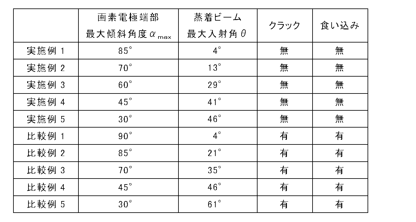
クラック、食い込みの有無は、各素子から断面TEM観察用試料を作製し、断面TEM写真で確認した。
表3に示す通り、本発明の条件を満たす実施例1~5においては、クラック、食い込み共に無く、本発明の条件を満たさない比較例1~5についてはクラック、食い込みが発生していた。この結果から、本発明の条件を満たすことにより、有機層におけるクラックや食い込みの発生を抑制することができることが明確である。クラックや食い込みの発生が抑制されていれば、画像表示の際の点欠陥を抑制することができる。
Claims (2)
- 基板上に複数の画素部を有する有機撮像素子であって、
前記基板上に互いに離間して配された、前記画素部の数に対応する複数の画素電極と、
該複数の画素電極上および該画素電極間に連続膜状に配された、前記複数の画素部に共有される、光電変換層を含む有機層と、
該有機層の上に配された、前記複数の画素部に共有される対向電極とを含み、
前記画素電極が、前記基板の基板面に傾斜角度α(但し、30°≦α≦85°)で傾斜する端部を有し、
前記複数の画素電極の端部の傾斜角度のうち最大の傾斜角度をαmaxとしたとき、前記有機層が、該有機層のガラス転移温度より低い蒸着基板温度条件下で前記基板面に対して(90°-αmax)より小さい入射角で入射する蒸着ビームにより蒸着されてなる膜であることを特徴とする有機撮像素子。 - 基板上に複数の画素部を有する有機撮像素子であって、該基板上に互いに離間して配置された複数の画素電極と、該複数の画素電極上および該画素電極間に連続膜状に配置された、前記複数の画素部に共有される、光電変換層を含む有機層と、該有機層の上に配置された、前記複数の画素部に共有される対向電極とを含む有機撮像素子の製造方法であって、
前記基板上に、前記複数の電極として、該基板の基板面に傾斜角度α(但し、30°≦α≦85°)で傾斜する端部を有する画素電極を複数形成する工程と、
前記複数の画素電極の端部の傾斜角度のうち最大の傾斜角度をαmaxとしたとき、該複数の画素電極の上方に、受光した光に応じて電荷を生成する光電変換層を含む有機層を、蒸着基板温度が該有機層のガラス転移温度より低い温度で、前記基板面に対して(90°-αmax)より小さい入射角で入射する蒸着ビームにより蒸着成膜する工程とを含むことを特徴とする有機撮像素子の製造方法。
Priority Applications (2)
| Application Number | Priority Date | Filing Date | Title |
|---|---|---|---|
| KR1020137030464A KR101613344B1 (ko) | 2011-04-20 | 2012-04-12 | 유기 촬상 소자 및 유기 촬상 소자의 제조 방법 |
| US14/058,172 US9040973B2 (en) | 2011-04-20 | 2013-10-18 | Organic image sensor and method of producing the same |
Applications Claiming Priority (2)
| Application Number | Priority Date | Filing Date | Title |
|---|---|---|---|
| JP2011-093809 | 2011-04-20 | ||
| JP2011093809A JP5694840B2 (ja) | 2011-04-20 | 2011-04-20 | 有機撮像素子および有機撮像素子の製造方法 |
Related Child Applications (1)
| Application Number | Title | Priority Date | Filing Date |
|---|---|---|---|
| US14/058,172 Continuation US9040973B2 (en) | 2011-04-20 | 2013-10-18 | Organic image sensor and method of producing the same |
Publications (1)
| Publication Number | Publication Date |
|---|---|
| WO2012144166A1 true WO2012144166A1 (ja) | 2012-10-26 |
Family
ID=47041300
Family Applications (1)
| Application Number | Title | Priority Date | Filing Date |
|---|---|---|---|
| PCT/JP2012/002535 Ceased WO2012144166A1 (ja) | 2011-04-20 | 2012-04-12 | 有機撮像素子および有機撮像素子の製造方法 |
Country Status (4)
| Country | Link |
|---|---|
| US (1) | US9040973B2 (ja) |
| JP (1) | JP5694840B2 (ja) |
| KR (1) | KR101613344B1 (ja) |
| WO (1) | WO2012144166A1 (ja) |
Families Citing this family (7)
| Publication number | Priority date | Publication date | Assignee | Title |
|---|---|---|---|---|
| JP5873847B2 (ja) | 2013-03-29 | 2016-03-01 | 富士フイルム株式会社 | 固体撮像素子および撮像装置 |
| TWI559062B (zh) * | 2013-12-09 | 2016-11-21 | 友達光電股份有限公司 | 主動元件陣列基板 |
| CN106132930A (zh) * | 2014-03-31 | 2016-11-16 | 索尼公司 | 用于有机光电转换层的二萘嵌苯类材料 |
| JP6429525B2 (ja) * | 2014-07-31 | 2018-11-28 | キヤノン株式会社 | 撮像装置、撮像システムおよび撮像装置の製造方法 |
| US10978514B2 (en) * | 2015-10-06 | 2021-04-13 | Sony Semiconductor Solutions Corporation | Solid-state imaging device, and method of manufacturing solid-state imaging device |
| CN113711376B (zh) * | 2019-04-17 | 2024-07-12 | 株式会社日本显示器 | 检测装置 |
| JP7599100B2 (ja) * | 2020-04-27 | 2024-12-13 | パナソニックIpマネジメント株式会社 | 撮像装置 |
Citations (3)
| Publication number | Priority date | Publication date | Assignee | Title |
|---|---|---|---|---|
| JP2002198171A (ja) * | 2000-12-26 | 2002-07-12 | Toyota Central Res & Dev Lab Inc | 有機電界発光素子の製造方法 |
| JP2004031262A (ja) * | 2002-06-28 | 2004-01-29 | Matsushita Electric Ind Co Ltd | 有機エレクトロルミネッセンスパネル |
| JP2011071469A (ja) * | 2009-08-28 | 2011-04-07 | Fujifilm Corp | 光電変換素子及び撮像素子 |
Family Cites Families (9)
| Publication number | Priority date | Publication date | Assignee | Title |
|---|---|---|---|---|
| JP4213832B2 (ja) | 1999-02-08 | 2009-01-21 | 富士フイルム株式会社 | 有機発光素子材料、それを使用した有機発光素子およびスチリルアミン化合物 |
| TW480554B (en) | 1999-07-22 | 2002-03-21 | Semiconductor Energy Lab | Semiconductor device and manufacturing method thereof |
| JP5010585B2 (ja) * | 2006-05-01 | 2012-08-29 | シャープ株式会社 | 液晶表示装置および液晶表示装置の製造方法 |
| JP2008177287A (ja) | 2007-01-17 | 2008-07-31 | Hitachi Cable Ltd | 化合物半導体ウェハ |
| JP2008177387A (ja) * | 2007-01-19 | 2008-07-31 | Fujifilm Corp | 放射線画像検出装置 |
| JP4637196B2 (ja) | 2007-03-16 | 2011-02-23 | 富士フイルム株式会社 | 固体撮像素子 |
| JP2009259978A (ja) | 2008-04-15 | 2009-11-05 | Konica Minolta Holdings Inc | 光電変換デバイスおよび放射線画像検出装置 |
| JP2010245366A (ja) * | 2009-04-08 | 2010-10-28 | Fujifilm Corp | 電子素子及びその製造方法、並びに表示装置 |
| JP5667752B2 (ja) * | 2009-08-20 | 2015-02-12 | 株式会社ジャパンディスプレイ | 立体映像表示装置 |
-
2011
- 2011-04-20 JP JP2011093809A patent/JP5694840B2/ja active Active
-
2012
- 2012-04-12 WO PCT/JP2012/002535 patent/WO2012144166A1/ja not_active Ceased
- 2012-04-12 KR KR1020137030464A patent/KR101613344B1/ko active Active
-
2013
- 2013-10-18 US US14/058,172 patent/US9040973B2/en active Active
Patent Citations (3)
| Publication number | Priority date | Publication date | Assignee | Title |
|---|---|---|---|---|
| JP2002198171A (ja) * | 2000-12-26 | 2002-07-12 | Toyota Central Res & Dev Lab Inc | 有機電界発光素子の製造方法 |
| JP2004031262A (ja) * | 2002-06-28 | 2004-01-29 | Matsushita Electric Ind Co Ltd | 有機エレクトロルミネッセンスパネル |
| JP2011071469A (ja) * | 2009-08-28 | 2011-04-07 | Fujifilm Corp | 光電変換素子及び撮像素子 |
Also Published As
| Publication number | Publication date |
|---|---|
| JP2012227364A (ja) | 2012-11-15 |
| JP5694840B2 (ja) | 2015-04-01 |
| KR101613344B1 (ko) | 2016-04-18 |
| US20140042416A1 (en) | 2014-02-13 |
| KR20140029450A (ko) | 2014-03-10 |
| US9040973B2 (en) | 2015-05-26 |
Similar Documents
| Publication | Publication Date | Title |
|---|---|---|
| JP5677890B2 (ja) | 光電変換素子、光電変換素子の製造方法、及び撮像素子 | |
| US8368058B2 (en) | Photoelectric conversion element and imaging device | |
| JP5694840B2 (ja) | 有機撮像素子および有機撮像素子の製造方法 | |
| JP5087304B2 (ja) | 固体撮像素子の製造方法 | |
| US9258463B2 (en) | Photoelectric conversion element and imaging device | |
| JP5288640B2 (ja) | 撮像素子及びその製造方法 | |
| JP2011228648A (ja) | 撮像素子 | |
| US8927321B2 (en) | Method for producing solid-state imaging device | |
| US9691999B2 (en) | Photoelectric conversion device vapor deposition material, photoelectric conversion device, sensor, and imaging device | |
| JP6128593B2 (ja) | 有機光電変換素子および撮像素子 | |
| WO2015076058A1 (ja) | 有機機能層付き基板およびその製造方法 | |
| JP2010062380A (ja) | 光電変換装置,光電変換装置の製造方法及び撮像装置 | |
| JP5683245B2 (ja) | 撮像素子及び撮像素子の製造方法 | |
| US20130214265A1 (en) | Solid-state imaging device and imaging apparatus | |
| JP5800682B2 (ja) | 光電変換素子の製造方法、および撮像素子の製造方法 | |
| JP2013093353A (ja) | 有機撮像素子 | |
| US20220158103A1 (en) | Optical sensor | |
| JP5525894B2 (ja) | 固体撮像素子の製造方法 | |
| JP2012119652A (ja) | 有機光電変換素子の製造方法、有機光電変換素子、撮像素子、撮像装置 |
Legal Events
| Date | Code | Title | Description |
|---|---|---|---|
| 121 | Ep: the epo has been informed by wipo that ep was designated in this application |
Ref document number: 12774655 Country of ref document: EP Kind code of ref document: A1 |
|
| NENP | Non-entry into the national phase |
Ref country code: DE |
|
| ENP | Entry into the national phase |
Ref document number: 20137030464 Country of ref document: KR Kind code of ref document: A |
|
| 122 | Ep: pct application non-entry in european phase |
Ref document number: 12774655 Country of ref document: EP Kind code of ref document: A1 |