WO2012141027A1 - 異方性導電フィルム - Google Patents
異方性導電フィルム Download PDFInfo
- Publication number
- WO2012141027A1 WO2012141027A1 PCT/JP2012/058917 JP2012058917W WO2012141027A1 WO 2012141027 A1 WO2012141027 A1 WO 2012141027A1 JP 2012058917 W JP2012058917 W JP 2012058917W WO 2012141027 A1 WO2012141027 A1 WO 2012141027A1
- Authority
- WO
- WIPO (PCT)
- Prior art keywords
- epoxy resin
- anisotropic conductive
- conductive film
- electronic component
- type epoxy
- Prior art date
- Legal status (The legal status is an assumption and is not a legal conclusion. Google has not performed a legal analysis and makes no representation as to the accuracy of the status listed.)
- Ceased
Links
Images


Classifications
-
- H—ELECTRICITY
- H01—ELECTRIC ELEMENTS
- H01R—ELECTRICALLY-CONDUCTIVE CONNECTIONS; STRUCTURAL ASSOCIATIONS OF A PLURALITY OF MUTUALLY-INSULATED ELECTRICAL CONNECTING ELEMENTS; COUPLING DEVICES; CURRENT COLLECTORS
- H01R4/00—Electrically-conductive connections between two or more conductive members in direct contact, i.e. touching one another; Means for effecting or maintaining such contact; Electrically-conductive connections having two or more spaced connecting locations for conductors and using contact members penetrating insulation
- H01R4/04—Electrically-conductive connections between two or more conductive members in direct contact, i.e. touching one another; Means for effecting or maintaining such contact; Electrically-conductive connections having two or more spaced connecting locations for conductors and using contact members penetrating insulation using electrically conductive adhesives
-
- C—CHEMISTRY; METALLURGY
- C08—ORGANIC MACROMOLECULAR COMPOUNDS; THEIR PREPARATION OR CHEMICAL WORKING-UP; COMPOSITIONS BASED THEREON
- C08G—MACROMOLECULAR COMPOUNDS OBTAINED OTHERWISE THAN BY REACTIONS ONLY INVOLVING UNSATURATED CARBON-TO-CARBON BONDS
- C08G59/00—Polycondensates containing more than one epoxy group per molecule; Macromolecules obtained by polymerising compounds containing more than one epoxy group per molecule using curing agents or catalysts which react with the epoxy groups
- C08G59/18—Macromolecules obtained by polymerising compounds containing more than one epoxy group per molecule using curing agents or catalysts which react with the epoxy groups ; e.g. general methods of curing
- C08G59/68—Macromolecules obtained by polymerising compounds containing more than one epoxy group per molecule using curing agents or catalysts which react with the epoxy groups ; e.g. general methods of curing characterised by the catalysts used
- C08G59/687—Macromolecules obtained by polymerising compounds containing more than one epoxy group per molecule using curing agents or catalysts which react with the epoxy groups ; e.g. general methods of curing characterised by the catalysts used containing sulfur
-
- C—CHEMISTRY; METALLURGY
- C08—ORGANIC MACROMOLECULAR COMPOUNDS; THEIR PREPARATION OR CHEMICAL WORKING-UP; COMPOSITIONS BASED THEREON
- C08L—COMPOSITIONS OF MACROMOLECULAR COMPOUNDS
- C08L63/00—Compositions of epoxy resins; Compositions of derivatives of epoxy resins
-
- C—CHEMISTRY; METALLURGY
- C09—DYES; PAINTS; POLISHES; NATURAL RESINS; ADHESIVES; COMPOSITIONS NOT OTHERWISE PROVIDED FOR; APPLICATIONS OF MATERIALS NOT OTHERWISE PROVIDED FOR
- C09D—COATING COMPOSITIONS, e.g. PAINTS, VARNISHES OR LACQUERS; FILLING PASTES; CHEMICAL PAINT OR INK REMOVERS; INKS; CORRECTING FLUIDS; WOODSTAINS; PASTES OR SOLIDS FOR COLOURING OR PRINTING; USE OF MATERIALS THEREFOR
- C09D5/00—Coating compositions, e.g. paints, varnishes or lacquers, characterised by their physical nature or the effects produced; Filling pastes
- C09D5/24—Electrically-conducting paints
-
- C—CHEMISTRY; METALLURGY
- C09—DYES; PAINTS; POLISHES; NATURAL RESINS; ADHESIVES; COMPOSITIONS NOT OTHERWISE PROVIDED FOR; APPLICATIONS OF MATERIALS NOT OTHERWISE PROVIDED FOR
- C09J—ADHESIVES; NON-MECHANICAL ASPECTS OF ADHESIVE PROCESSES IN GENERAL; ADHESIVE PROCESSES NOT PROVIDED FOR ELSEWHERE; USE OF MATERIALS AS ADHESIVES
- C09J7/00—Adhesives in the form of films or foils
- C09J7/10—Adhesives in the form of films or foils without carriers
-
- C—CHEMISTRY; METALLURGY
- C09—DYES; PAINTS; POLISHES; NATURAL RESINS; ADHESIVES; COMPOSITIONS NOT OTHERWISE PROVIDED FOR; APPLICATIONS OF MATERIALS NOT OTHERWISE PROVIDED FOR
- C09J—ADHESIVES; NON-MECHANICAL ASPECTS OF ADHESIVE PROCESSES IN GENERAL; ADHESIVE PROCESSES NOT PROVIDED FOR ELSEWHERE; USE OF MATERIALS AS ADHESIVES
- C09J9/00—Adhesives characterised by their physical nature or the effects produced, e.g. glue sticks
- C09J9/02—Electrically-conducting adhesives
-
- H—ELECTRICITY
- H10—SEMICONDUCTOR DEVICES; ELECTRIC SOLID-STATE DEVICES NOT OTHERWISE PROVIDED FOR
- H10W—GENERIC PACKAGES, INTERCONNECTIONS, CONNECTORS OR OTHER CONSTRUCTIONAL DETAILS OF DEVICES COVERED BY CLASS H10
- H10W72/00—Interconnections or connectors in packages
- H10W72/20—Bump connectors, e.g. solder bumps or copper pillars; Dummy bumps; Thermal bumps
-
- H—ELECTRICITY
- H10—SEMICONDUCTOR DEVICES; ELECTRIC SOLID-STATE DEVICES NOT OTHERWISE PROVIDED FOR
- H10W—GENERIC PACKAGES, INTERCONNECTIONS, CONNECTORS OR OTHER CONSTRUCTIONAL DETAILS OF DEVICES COVERED BY CLASS H10
- H10W72/00—Interconnections or connectors in packages
- H10W72/30—Die-attach connectors
-
- H—ELECTRICITY
- H10—SEMICONDUCTOR DEVICES; ELECTRIC SOLID-STATE DEVICES NOT OTHERWISE PROVIDED FOR
- H10W—GENERIC PACKAGES, INTERCONNECTIONS, CONNECTORS OR OTHER CONSTRUCTIONAL DETAILS OF DEVICES COVERED BY CLASS H10
- H10W72/00—Interconnections or connectors in packages
- H10W72/851—Dispositions of multiple connectors or interconnections
-
- H—ELECTRICITY
- H10—SEMICONDUCTOR DEVICES; ELECTRIC SOLID-STATE DEVICES NOT OTHERWISE PROVIDED FOR
- H10W—GENERIC PACKAGES, INTERCONNECTIONS, CONNECTORS OR OTHER CONSTRUCTIONAL DETAILS OF DEVICES COVERED BY CLASS H10
- H10W99/00—Subject matter not provided for in other groups of this subclass
-
- C—CHEMISTRY; METALLURGY
- C09—DYES; PAINTS; POLISHES; NATURAL RESINS; ADHESIVES; COMPOSITIONS NOT OTHERWISE PROVIDED FOR; APPLICATIONS OF MATERIALS NOT OTHERWISE PROVIDED FOR
- C09J—ADHESIVES; NON-MECHANICAL ASPECTS OF ADHESIVE PROCESSES IN GENERAL; ADHESIVE PROCESSES NOT PROVIDED FOR ELSEWHERE; USE OF MATERIALS AS ADHESIVES
- C09J2203/00—Applications of adhesives in processes or use of adhesives in the form of films or foils
- C09J2203/326—Applications of adhesives in processes or use of adhesives in the form of films or foils for bonding electronic components such as wafers, chips or semiconductors
-
- C—CHEMISTRY; METALLURGY
- C09—DYES; PAINTS; POLISHES; NATURAL RESINS; ADHESIVES; COMPOSITIONS NOT OTHERWISE PROVIDED FOR; APPLICATIONS OF MATERIALS NOT OTHERWISE PROVIDED FOR
- C09J—ADHESIVES; NON-MECHANICAL ASPECTS OF ADHESIVE PROCESSES IN GENERAL; ADHESIVE PROCESSES NOT PROVIDED FOR ELSEWHERE; USE OF MATERIALS AS ADHESIVES
- C09J2301/00—Additional features of adhesives in the form of films or foils
- C09J2301/30—Additional features of adhesives in the form of films or foils characterized by the chemical, physicochemical or physical properties of the adhesive or the carrier
- C09J2301/304—Additional features of adhesives in the form of films or foils characterized by the chemical, physicochemical or physical properties of the adhesive or the carrier the adhesive being heat-activatable, i.e. not tacky at temperatures inferior to 30°C
-
- C—CHEMISTRY; METALLURGY
- C09—DYES; PAINTS; POLISHES; NATURAL RESINS; ADHESIVES; COMPOSITIONS NOT OTHERWISE PROVIDED FOR; APPLICATIONS OF MATERIALS NOT OTHERWISE PROVIDED FOR
- C09J—ADHESIVES; NON-MECHANICAL ASPECTS OF ADHESIVE PROCESSES IN GENERAL; ADHESIVE PROCESSES NOT PROVIDED FOR ELSEWHERE; USE OF MATERIALS AS ADHESIVES
- C09J2301/00—Additional features of adhesives in the form of films or foils
- C09J2301/30—Additional features of adhesives in the form of films or foils characterized by the chemical, physicochemical or physical properties of the adhesive or the carrier
- C09J2301/314—Additional features of adhesives in the form of films or foils characterized by the chemical, physicochemical or physical properties of the adhesive or the carrier the adhesive layer and/or the carrier being conductive
-
- C—CHEMISTRY; METALLURGY
- C09—DYES; PAINTS; POLISHES; NATURAL RESINS; ADHESIVES; COMPOSITIONS NOT OTHERWISE PROVIDED FOR; APPLICATIONS OF MATERIALS NOT OTHERWISE PROVIDED FOR
- C09J—ADHESIVES; NON-MECHANICAL ASPECTS OF ADHESIVE PROCESSES IN GENERAL; ADHESIVE PROCESSES NOT PROVIDED FOR ELSEWHERE; USE OF MATERIALS AS ADHESIVES
- C09J2301/00—Additional features of adhesives in the form of films or foils
- C09J2301/40—Additional features of adhesives in the form of films or foils characterized by the presence of essential components
- C09J2301/408—Additional features of adhesives in the form of films or foils characterized by the presence of essential components additives as essential feature of the adhesive layer
-
- C—CHEMISTRY; METALLURGY
- C09—DYES; PAINTS; POLISHES; NATURAL RESINS; ADHESIVES; COMPOSITIONS NOT OTHERWISE PROVIDED FOR; APPLICATIONS OF MATERIALS NOT OTHERWISE PROVIDED FOR
- C09J—ADHESIVES; NON-MECHANICAL ASPECTS OF ADHESIVE PROCESSES IN GENERAL; ADHESIVE PROCESSES NOT PROVIDED FOR ELSEWHERE; USE OF MATERIALS AS ADHESIVES
- C09J2463/00—Presence of epoxy resin
-
- H—ELECTRICITY
- H10—SEMICONDUCTOR DEVICES; ELECTRIC SOLID-STATE DEVICES NOT OTHERWISE PROVIDED FOR
- H10W—GENERIC PACKAGES, INTERCONNECTIONS, CONNECTORS OR OTHER CONSTRUCTIONAL DETAILS OF DEVICES COVERED BY CLASS H10
- H10W72/00—Interconnections or connectors in packages
- H10W72/071—Connecting or disconnecting
- H10W72/0711—Apparatus therefor
- H10W72/07141—Means for applying energy, e.g. ovens or lasers
-
- H—ELECTRICITY
- H10—SEMICONDUCTOR DEVICES; ELECTRIC SOLID-STATE DEVICES NOT OTHERWISE PROVIDED FOR
- H10W—GENERIC PACKAGES, INTERCONNECTIONS, CONNECTORS OR OTHER CONSTRUCTIONAL DETAILS OF DEVICES COVERED BY CLASS H10
- H10W72/00—Interconnections or connectors in packages
- H10W72/071—Connecting or disconnecting
- H10W72/072—Connecting or disconnecting of bump connectors
-
- H—ELECTRICITY
- H10—SEMICONDUCTOR DEVICES; ELECTRIC SOLID-STATE DEVICES NOT OTHERWISE PROVIDED FOR
- H10W—GENERIC PACKAGES, INTERCONNECTIONS, CONNECTORS OR OTHER CONSTRUCTIONAL DETAILS OF DEVICES COVERED BY CLASS H10
- H10W72/00—Interconnections or connectors in packages
- H10W72/071—Connecting or disconnecting
- H10W72/073—Connecting or disconnecting of die-attach connectors
-
- H—ELECTRICITY
- H10—SEMICONDUCTOR DEVICES; ELECTRIC SOLID-STATE DEVICES NOT OTHERWISE PROVIDED FOR
- H10W—GENERIC PACKAGES, INTERCONNECTIONS, CONNECTORS OR OTHER CONSTRUCTIONAL DETAILS OF DEVICES COVERED BY CLASS H10
- H10W72/00—Interconnections or connectors in packages
- H10W72/071—Connecting or disconnecting
- H10W72/073—Connecting or disconnecting of die-attach connectors
- H10W72/07331—Connecting techniques
- H10W72/07332—Compression bonding, e.g. thermocompression bonding
-
- H—ELECTRICITY
- H10—SEMICONDUCTOR DEVICES; ELECTRIC SOLID-STATE DEVICES NOT OTHERWISE PROVIDED FOR
- H10W—GENERIC PACKAGES, INTERCONNECTIONS, CONNECTORS OR OTHER CONSTRUCTIONAL DETAILS OF DEVICES COVERED BY CLASS H10
- H10W72/00—Interconnections or connectors in packages
- H10W72/071—Connecting or disconnecting
- H10W72/073—Connecting or disconnecting of die-attach connectors
- H10W72/07331—Connecting techniques
- H10W72/07337—Connecting techniques using a polymer adhesive, e.g. an adhesive based on silicone or epoxy
- H10W72/07338—Connecting techniques using a polymer adhesive, e.g. an adhesive based on silicone or epoxy hardening the adhesive by curing, e.g. thermosetting
-
- H—ELECTRICITY
- H10—SEMICONDUCTOR DEVICES; ELECTRIC SOLID-STATE DEVICES NOT OTHERWISE PROVIDED FOR
- H10W—GENERIC PACKAGES, INTERCONNECTIONS, CONNECTORS OR OTHER CONSTRUCTIONAL DETAILS OF DEVICES COVERED BY CLASS H10
- H10W72/00—Interconnections or connectors in packages
- H10W72/071—Connecting or disconnecting
- H10W72/074—Connecting or disconnecting of anisotropic conductive adhesives
-
- H—ELECTRICITY
- H10—SEMICONDUCTOR DEVICES; ELECTRIC SOLID-STATE DEVICES NOT OTHERWISE PROVIDED FOR
- H10W—GENERIC PACKAGES, INTERCONNECTIONS, CONNECTORS OR OTHER CONSTRUCTIONAL DETAILS OF DEVICES COVERED BY CLASS H10
- H10W72/00—Interconnections or connectors in packages
- H10W72/20—Bump connectors, e.g. solder bumps or copper pillars; Dummy bumps; Thermal bumps
- H10W72/241—Dispositions, e.g. layouts
-
- H—ELECTRICITY
- H10—SEMICONDUCTOR DEVICES; ELECTRIC SOLID-STATE DEVICES NOT OTHERWISE PROVIDED FOR
- H10W—GENERIC PACKAGES, INTERCONNECTIONS, CONNECTORS OR OTHER CONSTRUCTIONAL DETAILS OF DEVICES COVERED BY CLASS H10
- H10W72/00—Interconnections or connectors in packages
- H10W72/20—Bump connectors, e.g. solder bumps or copper pillars; Dummy bumps; Thermal bumps
- H10W72/251—Materials
- H10W72/252—Materials comprising solid metals or solid metalloids, e.g. PbSn, Ag or Cu
-
- H—ELECTRICITY
- H10—SEMICONDUCTOR DEVICES; ELECTRIC SOLID-STATE DEVICES NOT OTHERWISE PROVIDED FOR
- H10W—GENERIC PACKAGES, INTERCONNECTIONS, CONNECTORS OR OTHER CONSTRUCTIONAL DETAILS OF DEVICES COVERED BY CLASS H10
- H10W72/00—Interconnections or connectors in packages
- H10W72/20—Bump connectors, e.g. solder bumps or copper pillars; Dummy bumps; Thermal bumps
- H10W72/261—Functions other than electrical connecting
-
- H—ELECTRICITY
- H10—SEMICONDUCTOR DEVICES; ELECTRIC SOLID-STATE DEVICES NOT OTHERWISE PROVIDED FOR
- H10W—GENERIC PACKAGES, INTERCONNECTIONS, CONNECTORS OR OTHER CONSTRUCTIONAL DETAILS OF DEVICES COVERED BY CLASS H10
- H10W72/00—Interconnections or connectors in packages
- H10W72/30—Die-attach connectors
- H10W72/321—Structures or relative sizes of die-attach connectors
- H10W72/325—Die-attach connectors having a filler embedded in a matrix
-
- H—ELECTRICITY
- H10—SEMICONDUCTOR DEVICES; ELECTRIC SOLID-STATE DEVICES NOT OTHERWISE PROVIDED FOR
- H10W—GENERIC PACKAGES, INTERCONNECTIONS, CONNECTORS OR OTHER CONSTRUCTIONAL DETAILS OF DEVICES COVERED BY CLASS H10
- H10W72/00—Interconnections or connectors in packages
- H10W72/30—Die-attach connectors
- H10W72/351—Materials of die-attach connectors
- H10W72/352—Materials of die-attach connectors comprising metals or metalloids, e.g. solders
-
- H—ELECTRICITY
- H10—SEMICONDUCTOR DEVICES; ELECTRIC SOLID-STATE DEVICES NOT OTHERWISE PROVIDED FOR
- H10W—GENERIC PACKAGES, INTERCONNECTIONS, CONNECTORS OR OTHER CONSTRUCTIONAL DETAILS OF DEVICES COVERED BY CLASS H10
- H10W72/00—Interconnections or connectors in packages
- H10W72/30—Die-attach connectors
- H10W72/351—Materials of die-attach connectors
- H10W72/353—Materials of die-attach connectors not comprising solid metals or solid metalloids, e.g. ceramics
- H10W72/354—Materials of die-attach connectors not comprising solid metals or solid metalloids, e.g. ceramics comprising polymers
-
- H—ELECTRICITY
- H10—SEMICONDUCTOR DEVICES; ELECTRIC SOLID-STATE DEVICES NOT OTHERWISE PROVIDED FOR
- H10W—GENERIC PACKAGES, INTERCONNECTIONS, CONNECTORS OR OTHER CONSTRUCTIONAL DETAILS OF DEVICES COVERED BY CLASS H10
- H10W74/00—Encapsulations, e.g. protective coatings
- H10W74/10—Encapsulations, e.g. protective coatings characterised by their shape or disposition
- H10W74/15—Encapsulations, e.g. protective coatings characterised by their shape or disposition on active surfaces of flip-chip devices, e.g. underfills
-
- H—ELECTRICITY
- H10—SEMICONDUCTOR DEVICES; ELECTRIC SOLID-STATE DEVICES NOT OTHERWISE PROVIDED FOR
- H10W—GENERIC PACKAGES, INTERCONNECTIONS, CONNECTORS OR OTHER CONSTRUCTIONAL DETAILS OF DEVICES COVERED BY CLASS H10
- H10W90/00—Package configurations
- H10W90/701—Package configurations characterised by the relative positions of pads or connectors relative to package parts
- H10W90/721—Package configurations characterised by the relative positions of pads or connectors relative to package parts of bump connectors
- H10W90/724—Package configurations characterised by the relative positions of pads or connectors relative to package parts of bump connectors between a chip and a stacked insulating package substrate, interposer or RDL
-
- H—ELECTRICITY
- H10—SEMICONDUCTOR DEVICES; ELECTRIC SOLID-STATE DEVICES NOT OTHERWISE PROVIDED FOR
- H10W—GENERIC PACKAGES, INTERCONNECTIONS, CONNECTORS OR OTHER CONSTRUCTIONAL DETAILS OF DEVICES COVERED BY CLASS H10
- H10W90/00—Package configurations
- H10W90/701—Package configurations characterised by the relative positions of pads or connectors relative to package parts
- H10W90/731—Package configurations characterised by the relative positions of pads or connectors relative to package parts of die-attach connectors
- H10W90/734—Package configurations characterised by the relative positions of pads or connectors relative to package parts of die-attach connectors between a chip and a stacked insulating package substrate, interposer or RDL
Definitions
- the present invention relates to an anisotropic conductive film in which conductive particles are dispersed in a thermosetting epoxy resin composition.
- an anisotropic conductive film (ACF) containing a general-purpose glycidyl ether type epoxy resin having a relatively low material cost as a main curing component is widely used.
- the conductive conductive film has not only good connection reliability but also low temperature fast curing from the viewpoint of preventing performance degradation of the IC chip due to heat and reducing the anisotropic conductive connection cost. From the viewpoint of effective use of expensive IC chips and wiring boards, there is also a demand for good repair properties and low material costs.
- general-purpose glycidyl ether type epoxy resins can be expected to have a certain degree of connection reliability among epoxy resin materials and have a relatively low material cost.
- the temperature had to be set to about 170 ° C. or higher, and it was difficult to say that the low-temperature rapid curability was sufficient, and there was a problem that sufficient repairability was not exhibited because the crosslinking density was excessively high.
- Patent Document 1 a cationic curing agent that can expect a rapid curing reaction as compared with a conventional general anionic curing agent as a curing agent
- Patent Document 2 glycidyl Attempts have been made to use alicyclic epoxy resins having higher reactivity instead of ether type epoxy resins
- the present invention is intended to solve the above-described problems of the conventional technology, and an epoxy resin-based anisotropic conductive film using a cationic curing agent is compared without using an alicyclic epoxy resin.
- Anisotropy that is excellent in both low-temperature fast-curing property and repairability, as well as excellent connection reliability and storage stability while using a general-purpose glycidyl ether type epoxy resin or its derivative
- An object is to provide a conductive film.
- thermosetting epoxy resin composition containing a cationic curing agent as a curing agent, ⁇ -alkyl glycidyl type epoxy having an alkyl group at the ⁇ -position of the epoxy ring as an epoxy resin constituting the epoxy resin composition, in addition to a general-purpose glycidyl ether type epoxy resin, an anionic polymerization of the epoxy resin due to steric hindrance
- the cationic polymerization system unexpectedly improved the low-temperature fast curability, and surprisingly improved the repairability, resulting in improved connection reliability and storage stability. Has been found to be excellent, and the present invention has been completed.
- the present invention provides an anisotropic conductive material in which conductive particles are dispersed in a thermosetting epoxy resin composition containing an epoxy resin, a cationic curing agent as a curing agent for the epoxy resin, and a film-forming resin.
- a thermosetting epoxy resin composition containing an epoxy resin, a cationic curing agent as a curing agent for the epoxy resin, and a film-forming resin.
- the epoxy resin contains a ⁇ -alkyl glycidyl type epoxy resin and a glycidyl ether type epoxy resin in a mass ratio of 9: 1 to 2: 8.
- the present invention is a method for manufacturing a connection structure in which a terminal of a first electronic component and a terminal of a second electronic component are anisotropically conductively connected by an anisotropic conductive film, A step of temporarily pasting the anisotropic conductive film of the present invention described above on the terminal of the first electronic component; A step of temporarily installing the second electronic component on the temporarily attached anisotropic conductive film so that the terminal faces the corresponding terminal of the first electronic component; and the second electronic component is heated by a bonder
- the manufacturing method includes the step of pressing against the first electronic component while heating and anisotropically connecting the terminal of the first electronic component and the terminal of the second electronic component.
- the present invention also provides a connection structure in which a terminal of a first electronic component and a terminal of a second electronic component are anisotropically conductively connected by the above-described anisotropic conductive film of the present invention.
- the epoxy resin-based anisotropic conductive film of the present invention using a cationic curing agent is a ⁇ -alkylglycidyl type epoxy resin as an epoxy resin constituting a thermosetting epoxy resin composition serving as a dispersion medium for conductive particles.
- a glycidyl ether type epoxy resin in combination with a glycidyl ether type epoxy resin at a predetermined ratio.
- the ⁇ -alkyl glycidyl type epoxy resin has a tertiary carbon that is thought to be able to stabilize the cationic species formed by the opening of the epoxy ring under the attack of the cationic species derived from the cationic polymerization initiator.
- the low temperature fast curability of the anisotropic conductive film can be improved, and the repair property, connection reliability and storage stability can be improved at the same time.
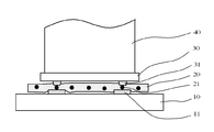
- FIG. 2 is a manufacturing process explanatory diagram of the connection structure subsequent to FIG. 1.
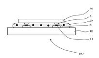
- FIG. 3 is an explanatory diagram of a manufacturing process of the connection structure subsequent to FIG. 2. It is a schematic sectional drawing of a connection structure.
- the present invention is an anisotropic conductive film in which conductive particles are dispersed in a thermosetting epoxy resin composition containing an epoxy resin, an epoxy resin curing agent, and a film-forming resin.
- thermosetting epoxy resin composition constituting the anisotropic conductive film of the present invention serves as a dispersion medium for conductive particles, forms a film as a whole, adheres to the adherend before curing, and after curing, It exhibits adhesive strength, and contains an epoxy resin, an epoxy resin curing agent, and a film-forming resin as described above.
- the epoxy resin contained in the thermosetting epoxy resin composition is a thermosetting component, and contains a ⁇ -alkyl glycidyl type epoxy resin and a glycidyl ether type epoxy resin.
- the anisotropic conductive film is compared with an anisotropic conductive film using a thermosetting epoxy resin composition composed of a general-purpose glycidyl ether type epoxy resin without using a ⁇ -methylglycidyl type epoxy resin.
- the low-temperature fast curability be improved, but also the repairability can be improved, and in addition, good connection reliability and storage stability can be realized.
- the ⁇ -alkyl glycidyl type epoxy resin is a compound represented by the following general formula (1).
- Y is an alkyl group such as a methyl group, an ethyl group, a propyl group, an isopropyl group, a butyl group, an isobutyl group, a pentyl group, a hexyl group, a cyclohexyl group, and in particular, a methyl group from the viewpoint of availability. Is preferred.
- X is an —O—, —NH— or —OCO— group. Among these, —O— is preferable from the viewpoint of ease of synthesis.
- N is a number of 2 or more.
- R is an aromatic, aliphatic or alicyclic polyalcohol compound residue, an aromatic, aliphatic or alicyclic polyamine compound residue, or an aromatic, aliphatic or alicyclic polycarboxylic acid compound residue .
- aromatic, aliphatic or alicyclic polyalcohol compound residues are preferred from the viewpoint of availability, and aromatic polyalcohol compound residues are particularly preferred.
- the compound of the formula (1) is prepared by dehydrochlorinating ⁇ -alkyl epichlorohydrin to a polyalcohol compound, polyamine compound or polycarboxylic acid compound. Therefore, the ⁇ -alkyl glycidyl type epoxy resin includes a monomer type and a prepolymer type (condensate). A preferred example of such a prepolymer type compound is shown in Formula (2).
- m is a number from 1 to 20.
- aromatic, aliphatic or alicyclic polyalcohol compounds include resorcinol, 4,4′-biphenol, bisphenol A, bisphenol F, 1,6-hexanediol, 1,4-butanediol, cyclohexane-1 , 3-diol and the like.
- aromatic, aliphatic or alicyclic polyamine compounds include o, m or p-phenylenediamine, 1,6-hexanediamine, 1,4-butanediamine, cyclohexane-1,3-diamine and the like.
- the aromatic, aliphatic or alicyclic polycarboxylic acid compound include phthalic acid, isophthalic acid, terephthalic acid, adipic acid, succinic acid and the like.
- the ⁇ -alkyl glycidyl type epoxy resin of the formula (1) include di ( ⁇ -alkyl glycidyl) resorcinol ether, bisphenol A type di ( ⁇ -alkyl glycidyl) ether, bisphenol F type di ( ⁇ -alkyl glycidyl). ) Ether and the like.
- di ( ⁇ -alkylglycidyl) resorcinol ether, particularly di ( ⁇ -methylglycidyl) resorcinol ether is preferable from the viewpoint that the low-temperature rapid curability of the anisotropic conductive film can be improved.
- the di ( ⁇ -methylglycidyl) resorcinol ether may be a monomer type or a prepolymer type.
- the glycidyl ether type epoxy resin used in combination with the ⁇ -alkyl glycidyl type epoxy resin is an epoxy resin in which a substituent such as an alkyl group does not exist in the glycidyl group, and is a general-purpose glycidyl ether type epoxy resin, particularly an alkylene oxide modified ( Preferably, 2 mol or more of alkylene oxide-modified glycidyl ether type epoxy resin can be preferably used.
- glycidyl ether type epoxy resins examples include bisphenol A type diglycidyl ether and its prepolymer (condensate), bisphenol F type diglycidyl ether and its prepolymer (condensate), phenol novolac type diglycidyl ether, and the like. be able to.
- ethylene oxide or propylene oxide modified bisphenol A type diglycidyl ether can be preferably used from the viewpoint of imparting good adhesive strength to the anisotropic conductive film.
- the epoxy resin contained in the thermosetting epoxy resin composition is the above-mentioned ⁇ -alkyl glycidyl type epoxy resin and glycidyl ether type epoxy resin in a mass ratio of 9: 1 to 2: 8, preferably 8: 2 to 4: It is contained at a ratio of 6. If the content of ⁇ -alkyl glycidyl type epoxy resin is larger than this mass ratio range, the connection reliability of the anisotropic conductive film tends to be lowered, and on the contrary, the repair property tends to be difficult to improve. There is.
- epoxy resin contained in the thermosetting epoxy resin composition other epoxy resins other than ⁇ -alkyl glycidyl type epoxy resins and glycidyl ether type epoxy resins, for example, 3,4-epoxycyclohexylmethyl 3,4 -An alicyclic epoxy resin such as epoxycyclohexanecarboxylate can be used in combination as long as the effects of the present invention are not impaired.
- thermosetting epoxy resin composition constituting the anisotropic conductive film of the present invention uses a cationic curing agent that is known to be effective for improving low-temperature rapid curing properties as a curing agent for epoxy resin.
- cationic curing agents known ones can be used.
- a chelate curing agent of a metal for example, aluminum, titanium, zinc, tin, etc.
- acetoacetic acid ester or diketones can be used.
- it is preferable to use an arylsulfonium salt-based curing agent because it has excellent reactivity at low temperatures and has a long pot life.
- arylsulfonium salt-based curing agents that can be suitably used in the present invention include structures having the structures shown in the following formulas (3) to (6).
- R a is a hydrogen atom, a COCH 3 group or a COOCH 3 group
- R b and R c are each a hydrogen atom, a halogen atom or a C 1 -C 4 alkyl group
- R d is a hydrogen atom An atom, a CH 3 group, an OCH 3 group or a halogen atom
- R e is a C 1 to C 4 alkyl group
- X is SbF 6 , AsF 6 , PF 6 or BF 4 .
- R f is a hydrogen atom, acetyl group, methoxycarbonyl group, methyl group, epoxycarbonyl group, t-butoxycarbonyl group, benzoyl group, phenoxycarbonyl group, benzyloxycarbonyl group, 9-fluoroenylmethoxy.
- R k is an ethoxy group, a phenyl group, a phenoxy group, a benzyloxy group, a chloromethyl group, a dichloromethyl group, a trifluoromethyl group or a trifluoromethyl group
- R 1 and R m are a hydrogen atom, a halogen atom, respectively.
- R n is a hydrogen atom, a methyl group, a methoxy group or a halogen atom
- R o is a C 1 -C 4 alkyl group
- X is SbF 6 , AsF 6 , PF 6 or BF 4 .
- R p is a hydrogen atom, acetyl group, methoxycarbonyl group, methyl group, epoxycarbonyl group, t-butoxycarbonyl group, benzoyl group, phenoxycarbonyl group, benzyloxycarbonyl group, 9-fluoroenylmethoxy.
- a carbonyl group or a p-methoxybenzylcarbonyl group, R q and R r are each a hydrogen atom, a halogen atom or a C 1 -C 4 alkyl group, and R s and R t are each a methyl group or an ethyl group.
- X is SbF 6 , AsF 6 , PF 6 or BF 4 .
- aryldiazonium salts for example, PP-33 (manufactured by ADEKA)
- aryliodonium salts for example, FC-509, FC-540 (manufactured by 3M), UVE1014 (manufactured by GE)
- the amount of the cationic curing agent used in the thermosetting epoxy resin composition is preferably 1 to 30 parts by mass, more preferably 1 to 10 parts by mass with respect to 100 parts by mass of the epoxy resin.
- the resin for film formation contained in the thermosetting epoxy resin composition constituting the anisotropic conductive film of the present invention is preferably a thermoplastic resin applied to a known resin for film formation of an anisotropic conductive film.
- a resin compatible with the epoxy resin of the thermosetting epoxy resin composition is preferable.
- phenoxy resin, polyester resin, urethane resin, polyamide resin, polyimide resin, polyolefin resin, etc. are used. These two or more can be used in combination.
- a phenoxy resin can be preferably used from the viewpoints of material cost, film formability, processability, connection reliability, and the like.
- the amount of the film-forming resin in the thermosetting epoxy resin composition constituting the anisotropic conductive film of the present invention is too small, the film-forming property tends to decrease, and if too large, the fluidity tends to decrease. Therefore, the amount is preferably 40 to 200 parts by mass, more preferably 50 to 150 parts by mass with respect to 100 parts by mass of the epoxy resin.
- conductive particles constituting the anisotropic conductive film of the present invention conductive particles used in known anisotropic conductive films can be employed.
- metal particles such as nickel, cobalt, silver, copper, gold, and palladium, metal-coated resin particles, and the like can be used, and two or more of these can be used in combination.
- Their particle shape and particle size can be appropriately determined according to the use environment and purpose of the anisotropic conductive film.
- thermosetting epoxy resin composition (that is, the total of the epoxy resin other than the conductive particles, the curing agent for the epoxy resin, and the resin for film formation) is preferably 0 1 to 50 parts by mass, more preferably 0.1 to 30 parts by mass.
- thermosetting epoxy resin composition constituting the anisotropic conductive film of the present invention is further subjected to stresses such as solvents, known silane coupling agents, colorants, flame retardants, fillers, polybutadiene particles, and the like as necessary. Additives such as a relaxation agent can be contained.
- An anisotropic conductive film of the present invention comprises an epoxy resin containing a ⁇ -alkyl glycidyl type epoxy resin and a glycidyl ether type epoxy resin in a mass ratio of 9: 1 to 2: 8, a curing agent for epoxy resin,
- a composition for forming an anisotropic conductive film is prepared by uniformly mixing a thermosetting epoxy resin composition containing a film-forming resin, conductive particles, and other additives according to a conventional method.
- the composition can be produced by forming into a film according to a known film forming method such as a calendering method or a casting method.
- An anisotropic conductive film is formed by uniformly mixing components other than conductive particles in advance to prepare a thermosetting epoxy resin composition, and uniformly dispersing the conductive particles in the composition by a conventional method.
- a composition for use may be prepared.
- the thickness of the anisotropic conductive film thus obtained can be appropriately determined according to the usage form of the anisotropic conductive film.
- the anisotropic conductive film of the present invention produces a connection structure in which a terminal formed on one side of a first electronic component and a terminal formed on one side of a second electronic component are anisotropically conductively connected. This can be preferably applied.
- the manufacturing method of the connection structure which uses the anisotropic conductive film of this invention which has process (a)-(c) is demonstrated for every process.
- the anisotropic conductive film 20 of the present invention is temporarily attached on the terminal 11 of the first electronic component 10. Temporary sticking can be performed by using a heating bonder 40 (see FIG. 3), which will be described later, and pressing while heating to a temperature at which the anisotropic conductive film 20 does not thermally cure but develops tackiness. Conductive particles 21 are dispersed in the anisotropic conductive film 20.
- Examples of the first electronic component 10 include a glass wiring board, a rigid wiring board, and a flexible wiring board.
- Examples of the terminal 11 include one formed on one side of the first electronic component 10 from a metal such as copper, nickel, aluminum, gold, or a complex oxide such as indium-titanium oxide according to a conventional method. Further, the thickness and wiring pitch of the terminal 11 can be appropriately determined according to the purpose of use of the first electronic component 10.
- Step (b)> the second electronic component 30 is placed on the temporarily attached anisotropic conductive film 20 so that the terminal 31 faces the corresponding terminal 11 of the first electronic component 10.
- Temporary installation can be performed by using a heating bonder 40 (see FIG. 3), which will be described later, and pressing while heating to a temperature at which the anisotropic conductive film 20 does not thermally cure but develops tackiness.
- the second electronic component 30 or the anisotropic conductive film 20 is misaligned during the temporary installation, for example, the first electronic component 10 side is heated with a hot plate as necessary, and is anisotropic.
- the conductive film 20 is softened, the second electronic component 30 is peeled off by a conventional method, and the thermosetting epoxy resin composition remaining on the surface of the first electronic component 10 or the second electronic component 30 is made of acetone or the like. It can be removed with an organic solvent. Thereby, good repairability can be realized.
- Examples of the second electronic component 30 include a semiconductor chip, a capacitor, an LED chip, and a flexible wiring board.
- Examples of the terminal 31 include electrodes (for example, bumps) formed on a single surface of the second electronic component 30 from a metal such as copper, nickel, aluminum, gold, or solder according to a conventional method. Further, the thickness and wiring pitch of the terminal 31 can be appropriately determined according to the purpose of use of the second electronic component 30.
- Step (c)> the second electronic component 30 is pressed against the first electronic component 10 while being heated by the heating bonder 40. Then, the conductive particles 21 sandwiched between the terminal 11 and the terminal 31 are crushed and electrically connected between the terminal 11 of the first electronic component 10 and the terminal 31 of the second electronic component 30. Thereby, as shown in FIG. 4, the connection structure 100 in which the terminal 11 of the first electronic component 10 and the terminal 31 of the second electronic component 30 are anisotropically conductively connected by the anisotropic conductive film 20. Is obtained.
- the heating bonder 40 used in this process (c) the well-known heating bonder used at the time of semiconductor device manufacture can be used. Moreover, as heating-pressing conditions, it can determine suitably according to the characteristic of the anisotropic conductive film to be used.
- connection structure 100 examples include a semiconductor device, a liquid crystal display device, an LED lighting device, and the like.
- This connection structure 100 is also an embodiment of the present invention.
- the anisotropic conductive film 20 is heat-cured.
- anisotropic conductive film of the present invention will be specifically described with reference to examples.
- Examples 1-12, Comparative Examples 1-7 ⁇ Creation of anisotropic conductive film> Thermoplastic resin (phenoxy resin), ⁇ -methyl glycidyl type epoxy resin A, glycidyl ether type epoxy resin B, silane coupling agent, cationic curing agent, stress relaxation in the blending ratio (part by mass) shown in Tables 1 and 2
- agent polybutadiene particles
- conductive particles uniformly using a stirrer
- DSC Different scanning calorimetry
- DSC calorific value reduction rate Thermal analysis of anisotropic conductive film immediately after production or after standing for 1 month, 2 months or 3 months at 30 ° C using a DSC apparatus (DSC-60, manufactured by Shimadzu Corporation) The total heat generation (j / g) was measured, and the total heat generation of the anisotropic conductive film left at 30 ° C. for 1 month, 2 months or 3 months with respect to the total heat generation amount of the anisotropic conductive film immediately after production The reduction rate (%) of the amount was calculated. In practice, the reduction rate (%) after one month is desirably 35% or less.
- Chip-on-film (COF) substrate substrate with a 50 ⁇ m pitch Cu8 ⁇ m thick-Sn plating electrode line formed on a 38 ⁇ m thick polyimide film surface
- ITO indium tin composite oxide
- an anisotropic conductive film slit to 1.5 mm at a predetermined position of the ITO solid glass substrate is passed through a Teflon (registered trademark) cushioning material having a thickness of 150 ⁇ m.
- a Teflon cushioning material having a thickness of 150 ⁇ m. was temporarily attached under the conditions of 70 ° C., 1 MPa, and 1 sec.
- a COF base material was temporarily installed on the temporarily attached anisotropic conductive film under the conditions of 80 ° C., 0.5 MPa, and 0.5 sec using the same crimping machine.
- connection structure was left in an environment of 85 ° C. and 85% RH for 500 hours. Then, the connection resistance value of the connection structure immediately after being left for 500 hours was measured using a digital multimeter (manufactured by Yokogawa Electric Corporation). In addition, the connection resistance value of the connection structure after being stored in an environment of 85 ° C. and 85% RH for 500 hours and further stored at 30 ° C. for 1 month, 2 months, or 3 months was measured in the same manner. In practice, the measured value is desirably 2 ⁇ or less.
- connection strength measurement The same connection structure as that created at the time of measuring the connection resistance value was prepared, and left in an environment of 85 ° C. and 85% RH for 500 hours. Next, the COF substrate of the connection structure was peeled in the 90 ° direction at a pulling speed of 50 mm / sec using a tensile tester (manufactured by AND), and the peel strength at that time was measured as the adhesive strength. It is desired that it is 6 N / cm or more practically.
- Chip-on-film (COF) substrate substrate with a 50 ⁇ m pitch Cu8 ⁇ m thick-Sn plating electrode line formed on a 38 ⁇ m thick polyimide film surface
- ITO indium tin composite oxide
- an anisotropic conductive film slit to 1.5 mm at a predetermined position of the ITO solid glass substrate is passed through a Teflon (registered trademark) cushioning material having a thickness of 150 ⁇ m.
- a Teflon cushioning material having a thickness of 150 ⁇ m. was temporarily attached under the conditions of 70 ° C., 1 MPa, and 1 sec.
- a COF base material was temporarily installed on the temporarily attached anisotropic conductive film under the conditions of 80 ° C., 0.5 MPa, and 0.5 sec using the same crimping machine to obtain a laminate.
- the laminate on which the COF base material was temporarily installed was placed on a hot plate heated to a temperature of 100 ° C. from the glass substrate side for 30 seconds, and then the COF base material was peeled off from the glass substrate.
- the thermosetting epoxy resin composition of the anisotropic conductive film remaining on the base material was wiped off with a cotton swab soaked with acetone, and the number of times of rubbing until all the resin composition was wiped off was counted. Practically, it is desired to be 30 times or less.
- Arylsulfonium salt curing agent (SI-60, Sanshin Chemical Co., Ltd.) + 3% stabilizer (p-hydroxyphenyldimethylsulfonium methylsulfate) * 9 Arylsulfonium salt curing agent (SI-60, Sanshin Chemical Co., Ltd.) + 5% stabilizer (p-hydroxyphenyldimethylsulfonium methylsulfate) * 10 Arylsulfonium salt curing agent (SI-60, Sanshin Chemical Industry Co., Ltd.) + 8% stabilizer (p-hydroxyphenyldimethylsulfonium methylsulfate) * 11 Arylsulfonium salt curing agent (SI-80, Sanshin Chemical Industry Co., Ltd.) + 3% stabilizer (p-hydroxyphenyldimethylsulfonium methylsulfate) * 12 Bright GNR, Nippon Chemical Industry Co., Ltd. * 13 CEL2021P, Daicel Corporation
- the anisotropic conductive films of Examples 1 to 12 were prepared by using a normal glycidyl ether type epoxy resin and a ⁇ -alkyl glycidyl type epoxy resin as the epoxy resin in a mass ratio of 9: 1 to 2: Since it is contained at a ratio of 8, there is no problem with the DSC exothermic start temperature and exothermic peak temperature, and the low temperature rapid curability is improved, and the repair property, connection reliability and storage stability are also improved at the same time. .
- the anisotropic conductive film of Comparative Example 1 in Table 2 uses only a normal glycidyl ether type epoxy resin as an epoxy resin, without using a ⁇ -alkyl glycidyl type epoxy resin.
- the thermocompression bonding condition of 160 ° C.-4 MPa-5 seconds there was a problem in the adhesive strength and repairability.
- the anisotropic conductive film of Comparative Example 2 does not use a ⁇ -alkyl glycidyl type epoxy resin, and compared with Comparative Example 1, half of a normal glycidyl ether type epoxy resin is used as an epoxy resin. Although it was replaced with an ether type epoxy resin, after all, only a glycidyl ether type epoxy resin was used, so as in Comparative Example 1, a relatively low temperature thermocompression bonding condition of 150 ° C.-4 MPa-5 seconds. There was a problem in the initial connection resistance and the adhesive strength in No. 1, and there was a problem in the repair property even under the thermocompression bonding condition of 160 ° C.-4 MPa-5 seconds.
- the anisotropic conductive film of Comparative Example 3 uses a ⁇ -alkyl glycidyl type epoxy resin and a glycidyl ether type epoxy resin in combination as an epoxy resin, but the mass ratio is 1: 9.
- the mass ratio is 1: 9.
- the anisotropic conductive film of Comparative Example 4 used only a ⁇ -alkyl glycidyl type epoxy resin as an epoxy resin, so there was no problem in the repair property under a relatively low temperature thermocompression bonding condition of 150 ° C.-4 MPa-5 seconds. However, there was a problem with the initial connection resistance and the adhesive strength, and there was also a problem with the adhesive strength even under the thermocompression bonding conditions of 160 ° C.-4 MPa-5 seconds.
- the anisotropic conductive film of Comparative Example 5 was replaced with an alicyclic epoxy resin as a part of the normal glycidyl ether type epoxy resin and the alkylene oxide-modified glycidyl ether type epoxy resin.
- an alicyclic epoxy resin as a part of the normal glycidyl ether type epoxy resin and the alkylene oxide-modified glycidyl ether type epoxy resin.
- the DSC reaction initiation temperature is low, and the repairability in thermocompression bonding conditions at relatively low and medium temperatures of 150 ° C and 160 ° C-4MPa-5 seconds. There was a problem.
- the anisotropic conductive films of Comparative Examples 6 and 7 were obtained by increasing the amount of stabilizer in the cationic curing agent from 3% to 5% and 8%, respectively, compared with Comparative Example 2, but as an epoxy resin, Similarly to Comparative Example 2, since a normal glycidyl ether type epoxy resin and an alkylene oxide-modified glycidyl ether type epoxy resin were used without using a ⁇ -alkyl glycidyl type epoxy resin, it was 170 ° C.-4 MPa-5 seconds. There was a problem with repairability under thermocompression bonding conditions.
- the epoxy resin-based anisotropic conductive film of the present invention using a cationic curing agent is a ⁇ -alkylglycidyl type epoxy resin as an epoxy resin constituting a thermosetting epoxy resin composition serving as a dispersion medium for conductive particles. Is used together with the glycidyl ether type epoxy resin at a predetermined ratio, so that the low-temperature fast curing property, the repair property, the connection reliability and the storage stability can be improved at the same time. Therefore, it is useful for manufacturing semiconductor devices and LED devices.
Landscapes
- Chemical & Material Sciences (AREA)
- Organic Chemistry (AREA)
- Health & Medical Sciences (AREA)
- Polymers & Plastics (AREA)
- Medicinal Chemistry (AREA)
- Chemical Kinetics & Catalysis (AREA)
- Materials Engineering (AREA)
- Wood Science & Technology (AREA)
- Engineering & Computer Science (AREA)
- Life Sciences & Earth Sciences (AREA)
- Non-Insulated Conductors (AREA)
- Adhesives Or Adhesive Processes (AREA)
- Wire Bonding (AREA)
- Conductive Materials (AREA)
- Adhesive Tapes (AREA)
- Epoxy Resins (AREA)
- Manufacturing Of Electrical Connectors (AREA)
Abstract
エポキシ樹脂とエポキシ樹脂用硬化剤と膜形成用樹脂とを含む熱硬化型エポキシ樹脂組成物中に導電性粒子が分散してなる異方性導電フィルムは、そのエポキシ樹脂として、β-アルキルグリシジル型エポキシ樹脂とグリシジルエーテル型エポキシ樹脂とを質量比9:1~2:8の割合で含有するものを使用する。β-アルキルグリシジル型エポキシ樹脂としては、ジ(β-メチルグリシジル)レゾルシノールエーテルが好ましく、グリシジルエーテル型エポキシ樹脂としては、アルキレンオキサイド変性グリシジルエーテル型エポキシ樹脂が好ましい。
Description
本発明は、熱硬化型エポキシ樹脂組成物中に導電性粒子が分散されている異方性導電フィルムに関する。
ICチップを配線基板に接続する際、比較的材料コストの低い汎用のグリシジルエーテル型エポキシ樹脂を主硬化成分とする異方性導電フィルム(ACF)が広く使用されているが、このような異方性導電フィルムに対しては、接続信頼性が良好であることは勿論、熱によるICチップの性能劣化の防止や異方性導電接続コストの低減という観点から低温速硬化性であること、更には、高価なICチップや配線基板の有効利用という観点から良好なリペア性を示すこと、そして材料コストが低いことも求められている。
ところで、汎用のグリシジルエーテル型エポキシ樹脂は、エポキシ樹脂材料の中では、ある程度の接続信頼性が期待でき、しかも比較的低い材料コストのものであるが、反応性が十分とは言えず、そのため硬化温度を約170℃以上に設定せざるを得ず、低温速硬化性が十分とは言い難く、しかも架橋密度が過度に高いために十分なリペア性を示さないという問題があった。
このため、これらの課題を解決するアプローチとして、硬化剤として従来の一般的なアニオン系硬化剤に比べて迅速な硬化反応が期待できるカチオン系硬化剤を使用すること(特許文献1)や、グリシジルエーテル型エポキシ樹脂に代えて、反応性のより高い脂環式エポキシ樹脂を使用することが試みられている(特許文献2)。
しかしながら、カチオン系硬化剤を使用した場合、低温速硬化性の改善が図られるものの、依然としてリペア性が不十分であるという問題があった。また、カチオン系硬化剤の使用に加え、脂環式エポキシ樹脂を使用した場合、グリシジルエーテル型エポキシ樹脂に比べ、低温速硬化性がより改善される反面、材料コストが高く、また、依然としてリペア性が不十分であり、異方性導電フィルムとしての保存安定性が低下するという問題があった。更に、グリシジルエーテル型エポキシ樹脂に比べてより疎水性であるため、被着体に対する接着力が高温高湿条件下でのエージング処理後に低下し、それに伴い接続信頼性も低下する傾向があった。
本発明は、以上の従来の技術の課題を解決しようとするものであり、カチオン系硬化剤を使用するエポキシ樹脂ベースの異方性導電フィルムにおいて、脂環式エポキシ樹脂を使用することなく、比較的低い材料コストの汎用のグリシジルエーテル型エポキシ樹脂もしくはその誘導体を使用しながらも、低温速硬化性及びリペア性の双方において優れ、さらには接続信頼性及び保存安定性にも優れている異方性導電フィルムを提供することを目的とする。
本発明者らは、硬化剤としてカチオン系硬化剤を含有する熱硬化型エポキシ樹脂組成物中に導電性粒子が分散した異方性導電フィルムの特に低温速硬化性を改善するために、熱硬化型エポキシ樹脂組成物を構成するエポキシ樹脂として、汎用のグリシジルエーテル型エポキシ樹脂に加え、エポキシ樹脂のアニオン重合を立体障害により阻害し得るアルキル基をエポキシ環のβ位に有するβ-アルキルグリシジル型エポキシ樹脂を併用してみたところ、アニオン重合系の場合と異なりカチオン重合系では予想外にも低温速硬化性が改善され、更に驚くべきことにリペア性も改善され、接続信頼性及び保存安定性にも優れたものとなることを見出し、本発明を完成させるに至った。
即ち、本発明は、エポキシ樹脂と、エポキシ樹脂用硬化剤としてカチオン系硬化剤と、膜形成用樹脂とを含む熱硬化型エポキシ樹脂組成物中に導電性粒子が分散している異方性導電フィルムにおいて、
該エポキシ樹脂が、β-アルキルグリシジル型エポキシ樹脂とグリシジルエーテル型エポキシ樹脂とを質量比9:1~2:8の割合で含有する異方性導電フィルムを提供する。
該エポキシ樹脂が、β-アルキルグリシジル型エポキシ樹脂とグリシジルエーテル型エポキシ樹脂とを質量比9:1~2:8の割合で含有する異方性導電フィルムを提供する。
また、本発明は、第1の電子部品の端子と第2の電子部品の端子とが異方性導電フィルムにより異方性導電接続されている接続構造体の製造方法であって、
第1の電子部品の端子上に、前述の本発明の異方性導電フィルムを仮貼りする工程、
仮貼りされた異方性導電フィルム上に、第2の電子部品を、その端子が第1の電子部品の対応する端子と対向するように仮設置する工程、及び
第2の電子部品を加熱ボンダーで加熱しながら第1の電子部品に対して押圧し、第1の電子部品の端子と第2の電子部品の端子とを異方性導電接続する工程
を有する製造方法を提供する。
第1の電子部品の端子上に、前述の本発明の異方性導電フィルムを仮貼りする工程、
仮貼りされた異方性導電フィルム上に、第2の電子部品を、その端子が第1の電子部品の対応する端子と対向するように仮設置する工程、及び
第2の電子部品を加熱ボンダーで加熱しながら第1の電子部品に対して押圧し、第1の電子部品の端子と第2の電子部品の端子とを異方性導電接続する工程
を有する製造方法を提供する。
また、本発明は、第1の電子部品の端子と第2の電子部品の端子とが前述の本発明の異方性導電フィルムにより異方性導電接続されてなる接続構造体を提供する。
カチオン系硬化剤を使用する本発明のエポキシ樹脂ベースの異方性導電フィルムは、導電性粒子の分散媒となる熱硬化型エポキシ樹脂組成物を構成するエポキシ樹脂として、β-アルキルグリシジル型エポキシ樹脂をグリシジルエーテル型エポキシ樹脂と所定割合で併用する。β-アルキルグリシジル型エポキシ樹脂は、カチオン系重合開始剤由来のカチオン種の攻撃を受けてエポキシ環が開環して形成されるカチオン種を安定化し得ると考えられる3級炭素を有するため、結果的に異方性導電フィルムの低温速硬化性を改善し、しかもリペア性、接続信頼性及び保存安定性についても同時に改善できる。
本発明は、エポキシ樹脂とエポキシ樹脂用硬化剤と膜形成用樹脂とを含む熱硬化型エポキシ樹脂組成物中に導電性粒子が分散している異方性導電フィルムである。
本発明の異方性導電フィルムを構成する熱硬化型エポキシ樹脂組成物は、導電性粒子の分散媒となり、全体として膜を形成し、被着体に対し硬化前には粘着力、硬化後には接着力を発揮するものであり、前述したように、エポキシ樹脂とエポキシ樹脂用硬化剤と膜形成用樹脂とを含有する。
本発明において、熱硬化型エポキシ樹脂組成物が含有するエポキシ樹脂は、熱硬化成分であり、β-アルキルグリシジル型エポキシ樹脂と、グリシジルエーテル型エポキシ樹脂とを含有する。これにより、異方性導電フィルムは、β-メチルグリシジル型エポキシ樹脂を使用せずに汎用のグリシジルエーテル型エポキシ樹脂から構成した熱硬化型エポキシ樹脂組成物を使用した異方性導電フィルムに比べて低温速硬化性を改善することができるだけでなく、更にリペア性も改善でき、加えて、良好な接続信頼性及び保存安定性を実現することができる。
β-アルキルグリシジル型エポキシ樹脂とは、以下の一般式(1)で表される化合物である。

式(1)中、Yはメチル基、エチル基、プロピル基、イソプロピル基、ブチル基、イソブチル基、ペンチル基、ヘキシル基、シクロヘキシル基等のアルキル基であり、中でも入手容易性の点からメチル基が好ましい。Xは-O-、-NH-又は-OCO-基である。中でも、合成容易性の点から-O-が好ましい。また、nは2以上の数である。Rは、芳香族、脂肪族あるいは脂環式ポリアルコール化合物残基、芳香族、脂肪族あるいは脂環式ポリアミン化合物残基、又は芳香族、脂肪族あるいは脂環式ポリカルボン酸化合物残基である。中でも、入手容易性の点から、芳香族、脂肪族あるいは脂環式ポリアルコール化合物残基が好ましく、特に、芳香族ポリアルコール化合物残基が好ましい。ここで、式(1)の化合物は、β-アルキルエピクロロヒドリンを、ポリアルコール化合物、ポリアミン化合物あるいはポリカルボン酸化合物に脱塩酸反応させることにより調製されるものであり、脱塩酸反応は逐次的に進行するため、β-アルキルグリシジル型エポキシ樹脂には、モノマータイプのものや、プレポリマータイプ(縮合物)のものが包含される。このようなプレポリマータイプの化合物の好ましい例を式(2)に示す。ここでmは、1~20の数である。

このような芳香族、脂肪族あるいは脂環式ポリアルコール化合物としては、レゾルシノール、4,4′-ビフェノール、ビスフェノールA、ビスフェノールF、1,6-ヘキサンジオール、1,4-ブタンジオール、シクロヘキサン-1,3-ジオール等を挙げることができる。芳香族、脂肪族あるいは脂環式ポリアミン化合物としては、o,m又はp-フェニレンジアミン、1,6-ヘキサンジアミン、1,4-ブタンジアミン、シクロヘキサン-1,3-ジアミン等を挙げることができる。芳香族、脂肪族あるいは脂環式ポリカルボン酸化合物としては、フタル酸、イソフタル酸、テレフタル酸、アジピン酸、コハク酸等を挙げることができる。
式(1)のβ-アルキルグリシジル型エポキシ樹脂の好ましい具体的としては、ジ(β-アルキルグリシジル)レゾルシノールエーテル、ビスフェノールA型ジ(β-アルキルグリシジル)エーテル、ビスフェノールF型ジ(β-アルキルグリシジル)エーテル等が挙げられる。中でも、異方性導電フィルムの低温速硬化性を改善できる点からジ(β-アルキルグリシジル)レゾルシノールエーテル、特にジ(β-メチルグリシジル)レゾルシノールエーテルが好ましい。なお、このジ(β-メチルグリシジル)レゾルシノールエーテルは、モノマータイプでもよく、プレポリマータイプでもよい。
他方、β-アルキルグリシジル型エポキシ樹脂と併用するグリシジルエーテル型エポキシ樹脂としては、グリシジル基にアルキル基などの置換基が存在しないエポキシ樹脂であり、汎用のグリシジルエーテル型エポキシ樹脂、中でもアルキレンオキサイド変性(好ましくは2モル以上のアルキレンオキサイド変性)グリシジルエーテル型エポキシ樹脂を好ましく使用することができる。このようなグリシジルエーテル型エポキシ樹脂としては、ビスフェノールA型ジグリシジルエーテル及びそのプレポリマー(縮合物)、ビスフェノールF型ジグリシジルエーテル及びそのプレポリマー(縮合物)、フェノールノボラック型ジグリシジルエーテル等を挙げることができる。中でも、異方性導電フィルムに良好な接着強度を付与できる点からエチレンオキサイド又はプロピレンオキサイド変性ビスフェノールA型ジグリシジルエーテルを好ましく使用することができる。
熱硬化型エポキシ樹脂組成物が含有するエポキシ樹脂は、上述したβ-アルキルグリシジル型エポキシ樹脂とグリシジルエーテル型エポキシ樹脂とを、質量比9:1~2:8、好ましくは8:2~4:6の割合で含有する。この質量比範囲よりもβ-アルキルグリシジル型エポキシ樹脂の含有量が多くなると、異方性導電フィルムの接続信頼性が低下する傾向があり、反対に少なくなると、そのリペア性が改善し難くなる傾向がある。
本発明において、熱硬化型エポキシ樹脂組成物が含有するエポキシ樹脂として、β-アルキルグリシジル型エポキシ樹脂及びグリシジルエーテル型エポキシ樹脂以外の他のエポキシ樹脂、例えば、3,4-エポキシシクロヘキシルメチル 3,4-エポキシシクロヘキサンカルボキシレートなどの脂環式エポキシ樹脂を、本発明の効果を損なわない範囲で併用することができる。
本発明の異方性導電フィルムを構成する熱硬化型エポキシ樹脂組成物は、エポキシ樹脂用硬化剤として、低温速硬化性の改善に有効なことが知られているカチオン系硬化剤を使用する。このようなカチオン系硬化剤としては、公知のものを使用することができ、例えば、アリールジアゾニウム塩系硬化剤、アリールヨードニウム塩系硬化剤、アリールスルホニウム塩系硬化剤、アレン-イオン錯体系硬化剤、金属(例えば、アルミニウム、チタン、亜鉛、錫など)とアセト酢酸エステルまたはジケトン類とのキレート系硬化剤等を使用することができる。特に、低温での反応性に優れ、ポットライフが長い点から、アリールスルホニウム塩系硬化剤を使用することが好ましい。
本発明において好適に用いることのできるアリールスルホニウム塩系硬化剤として、以下の式(3)~(6)に示されたような構造のものが例示される。

式(3)中、Raは水素原子、COCH3基又はCOOCH3基であり、Rb及びRcはそれぞれ水素原子、ハロゲン原子又はC1~C4のアルキル基であり、Rdは水素原子、CH3基、OCH3基又はハロゲン原子であり、ReはC1~C4のアルキル基であり、XはSbF6、AsF6、PF6又はBF4である。
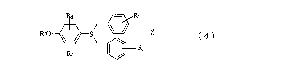
式(4)中、Rfは水素原子、アセチル基、メトキシカルボニル基、メチル基、エポキシカルボニル基、t-ブトキシカルボニル基、ベンゾイル基、フェノキシカルボニル基、ベンジルオキシカルボニル基、9-フロオレニルメトキシカルボニル基又はp-メトキシベンジルカルボニル基であり、Rg及びRhはそれぞれ水素原子、ハロゲン原子又はC1~C4のアルキル基であり、Ri及びRjはそれぞれ水素原子、メチル基、メトキシ基又はハロゲン原子であり、XはSbF6、AsF6、PF6又はBF4である。

式(5)中、Rkはエトキシ基、フェニル基、フェノキシ基、ベンジルオキシ基、クロルメチル基、ジクロルメチル基、トリクロルメチル基又はトリフルオロメチル基であり、Rl及びRmはそれぞれ水素原子、ハロゲン原子又はC1~C4のアルキル基であり、Rnは水素原子、メチル基、メトキシ基又はハロゲン原子であり、RoはC1~C4のアルキル基であり、XはSbF6、AsF6、PF6又はBF4である。

式(6)中、Rpは水素原子、アセチル基、メトキシカルボニル基、メチル基、エポキシカルボニル基、t-ブトキシカルボニル基、ベンゾイル基、フェノキシカルボニル基、ベンジルオキシカルボニル基、9-フロオレニルメトキシカルボニル基又はp-メトキシベンジルカルボニル基であり、Rq及びRrはそれぞれ水素原子、ハロゲン原子又はC1~C4のアルキル基であり、Rs及びRtはそれぞれメチル基又はエチル基であり、XはSbF6、AsF6、PF6又はBF4である。
本発明で使用し得る市販されているカチオン系硬化剤の具体例としては、例えば、アリールジアゾニウム塩[例えば、PP-33((株)ADEKA製)]、アリールヨードニウム塩、アリールスルホニウム塩[例えば、FC-509、FC-540(3M社製)、UVE1014(G.E.社製)、UVI-6974、UVI-6970、UVI-6990、UVI-6950(ユニオン・カーバイド社製)、SP-170、SP-150、CP-66、CP-77など((株)ADEKA製)]、SI-60L、SI-80L、SI-100L、SI-110L(三新化学工業(株)製)、アレン-イオン錯体[例えば、CG-24-61(BASF社製)]が挙げられる。
熱硬化型エポキシ樹脂組成物におけるカチオン系硬化剤の使用量は、少なすぎると硬化不良が生ずる傾向があり、多すぎると保存安定性が低下する傾向があり、また、この範囲で使用することにより、耐熱性、透明性、耐候性等の良好な硬化物を得ることができるので、好ましくはエポキシ樹脂100質量部に対し、1~30質量部、より好ましくは1~10質量部である。
本発明の異方性導電フィルムを構成する熱硬化型エポキシ樹脂組成物が含有する膜形成用樹脂としては、公知の異方性導電フィルムの膜形成用樹脂に適用されている熱可塑性樹脂を好ましく使用することができる。このような膜形成用樹脂としては、熱硬化型エポキシ樹脂組成物のエポキシ樹脂と相溶するものが好ましく、例えば、フェノキシ樹脂、ポリエステル樹脂、ウレタン樹脂、ポリアミド樹脂、ポリイミド樹脂、ポリオレフィン樹脂などを使用することができ、これらの2種以上を併用することができる。これらの中でも、材料コスト、成膜性、加工性、接続信頼性等の観点から、フェノキシ樹脂を好ましく使用することができる。
本発明の異方性導電フィルムを構成する熱硬化型エポキシ樹脂組成物における膜形成用樹脂の配合量は、少なすぎるとフィルム形成性が低下する傾向があり、多すぎると流動性が低下する傾向があるので、エポキシ樹脂100質量部に対し、好ましくは40~200質量部、より好ましくは50~150質量部である。
本発明の異方性導電フィルムを構成する導電性粒子としては、公知の異方性導電フィルムで使用されている導電性粒子を採用することができる。例えば、ニッケル、コバルト、銀、銅、金、パラジウムなどの金属粒子、金属被覆樹脂粒子などを挙げることができ、これらの2種以上を併用することができる。それらの粒子形状及び粒径は、異方性導電フィルムの使用環境、使用目的などに応じて適宜決定することができる。
このような導電性粒子の熱硬化型エポキシ樹脂組成物に対する配合割合は、導電性粒子が少なすぎると安定した異方性導電接続が困難になる傾向があり、多すぎるとフィルムの平面方向における導電性粒子の導通が生じ易くなるので、熱硬化型エポキシ樹脂組成物(即ち、導電性粒子以外のエポキシ樹脂、エポキシ樹脂用硬化剤及び膜形成用樹脂の合計)100質量部に対し、好ましくは0.1~50質量部、より好ましくは0.1~30質量部である。
本発明の異方性導電フィルムを構成する熱硬化型エポキシ樹脂組成物は、更に必要に応じて、溶剤や、公知のシランカップリング剤、着色剤、難燃剤、充填剤、ポリブタジエン粒子等の応力緩和剤等の添加剤を含有することができる。
本発明の異方性導電フィルムは、β-アルキルグリシジル型エポキシ樹脂とグリシジルエーテル型エポキシ樹脂とを質量比9:1~2:8の割合で含有するエポキシ樹脂と、エポキシ樹脂用硬化剤と、膜形成用樹脂とを含む熱硬化型エポキシ樹脂組成物と、導電性粒子と、他の添加剤とを常法に従って均一に混合することにより異方性導電フィルム形成用組成物を調製し、その組成物をカレンダー法、キャスト法等の公知のフィルム形成法に従って、フィルム化することにより製造することができる。なお、導電性粒子以外の成分を予め均一に混合して熱硬化型エポキシ樹脂組成物を調製し、その組成物中に導電性粒子を常法により均一に分散させることにより異方性導電フィルム形成用組成物を調製してもよい。
このようにして得られた異方性導電フィルムの厚みは、異方性導電フィルムの使用形態などに応じて適宜決定することができる。
本発明の異方性導電フィルムは、第1の電子部品の片面に形成された端子と第2の電子部品の片面に形成された端子とが異方性導電接続されている接続構造体を製造する際に好ましく適用することができる。以下に、工程(a)~(c)を有する、本発明の異方性導電フィルムを使用する接続構造体の製造方法について工程毎に説明する。
<工程(a)>
図1に示すように、第1の電子部品10の端子11上に、本発明の異方性導電フィルム20を仮貼りする。仮貼りは、後述する加熱ボンダー40(図3参照)を使用し、異方性導電フィルム20が熱硬化しないが粘着性を発現する温度に加熱しながら押圧することにより行うことができる。異方性導電フィルム20中には、導電性粒子21が分散している。
図1に示すように、第1の電子部品10の端子11上に、本発明の異方性導電フィルム20を仮貼りする。仮貼りは、後述する加熱ボンダー40(図3参照)を使用し、異方性導電フィルム20が熱硬化しないが粘着性を発現する温度に加熱しながら押圧することにより行うことができる。異方性導電フィルム20中には、導電性粒子21が分散している。
第1の電子部品10としては、ガラス配線基板、リジッド配線基板、フレキシブル配線基板などを挙げることができる。端子11としては、第1の電子部品10の片面に、銅、ニッケル、アルミ、金等の金属やインジウム-チタン酸化物等の複合酸化物から常法に従って形成されたものを挙げることができる。また、端子11の厚みや配線ピッチは、第1の電子部品10の使用目的等に応じて適宜決定することができる。
<工程(b)>
次に、図2に示すように、仮貼りされた異方性導電フィルム20上に、第2の電子部品30を、その端子31が第1の電子部品10の対応する端子11と対向するように仮設置する。仮設置は、後述する加熱ボンダー40(図3参照)を使用し、異方性導電フィルム20が熱硬化しないが粘着性を発現する温度に加熱しながら押圧することにより行うことができる。この仮設置の際、第2の電子部品30又は異方性導電フィルム20の位置ズレが生じた場合、必要に応じて、例えば、第1の電子部品10側を熱板で加熱して異方性導電フィルム20を軟化させ、第2の電子部品30を常法により引き剥がし、第1の電子部品10又は第2の電子部品30の表面に残存した熱硬化型エポキシ樹脂組成物をアセトンなどの有機溶剤で除去することができる。これにより良好なリペア性を実現することができる。
次に、図2に示すように、仮貼りされた異方性導電フィルム20上に、第2の電子部品30を、その端子31が第1の電子部品10の対応する端子11と対向するように仮設置する。仮設置は、後述する加熱ボンダー40(図3参照)を使用し、異方性導電フィルム20が熱硬化しないが粘着性を発現する温度に加熱しながら押圧することにより行うことができる。この仮設置の際、第2の電子部品30又は異方性導電フィルム20の位置ズレが生じた場合、必要に応じて、例えば、第1の電子部品10側を熱板で加熱して異方性導電フィルム20を軟化させ、第2の電子部品30を常法により引き剥がし、第1の電子部品10又は第2の電子部品30の表面に残存した熱硬化型エポキシ樹脂組成物をアセトンなどの有機溶剤で除去することができる。これにより良好なリペア性を実現することができる。
第2の電子部品30としては、半導体チップ、コンデンサ、LEDチップ、フレキシブル配線基板等を挙げることができる。端子31としては、第2の電子部品30の片面に、銅、ニッケル、アルミ、金、ハンダ等の金属から常法に従って形成された電極(例えばバンプ)を挙げることができる。また、端子31の厚みや配線ピッチは、第2の電子部品30の使用目的等に応じて適宜決定することができる。
<工程(c)>
次に、図3に示すように、第2の電子部品30を加熱ボンダー40で加熱しながら第1の電子部品10に対して押圧する。すると、端子11と端子31とに挟まれた導電性粒子21が潰れ、第1の電子部品10の端子11と第2の電子部品30の端子31との間で電気的に導通する。これにより、図4に示すように、第1の電子部品10の端子11と第2の電子部品30の端子31とが異方性導電フィルム20により異方性導電接続されている接続構造体100が得られる。
次に、図3に示すように、第2の電子部品30を加熱ボンダー40で加熱しながら第1の電子部品10に対して押圧する。すると、端子11と端子31とに挟まれた導電性粒子21が潰れ、第1の電子部品10の端子11と第2の電子部品30の端子31との間で電気的に導通する。これにより、図4に示すように、第1の電子部品10の端子11と第2の電子部品30の端子31とが異方性導電フィルム20により異方性導電接続されている接続構造体100が得られる。
なお、この工程(c)において使用する加熱ボンダー40としては、半導体装置製造時に使用されているような公知の加熱ボンダーを使用することができる。また、加熱加圧条件としては、使用する異方性導電フィルムの特性に応じて適宜決定することができる。
このようにして得られる接続構造体100の具体例としては、半導体装置、液晶表示装置、LED照明装置等が挙げられる。この接続構造体100も本発明の一態様である。なお、接続構造体100においては、異方性導電フィルム20は熱硬化されたものとなっている。
以下に、本発明の異方性導電フィルムを実施例により具体的に説明する。
実施例1~12、比較例1~7
<異方性導電フィルムの作成>
表1及び2の配合割合(質量部基準)で、熱可塑性樹脂(フェノキシ樹脂)、β-メチルグリシジル型エポキシ樹脂A、グリシジルエーテル型エポキシ樹脂B、シランカップリング剤、カチオン系硬化剤、応力緩和剤(ポリブタジエン粒子)及び導電性粒子を、撹拌装置を用いて均一に混合し、剥離フィルム上に乾燥厚が20μmとなるように塗布し、70℃のオーブン中で乾燥することにより、異方性導電フィルムを作成した。
<異方性導電フィルムの作成>
表1及び2の配合割合(質量部基準)で、熱可塑性樹脂(フェノキシ樹脂)、β-メチルグリシジル型エポキシ樹脂A、グリシジルエーテル型エポキシ樹脂B、シランカップリング剤、カチオン系硬化剤、応力緩和剤(ポリブタジエン粒子)及び導電性粒子を、撹拌装置を用いて均一に混合し、剥離フィルム上に乾燥厚が20μmとなるように塗布し、70℃のオーブン中で乾燥することにより、異方性導電フィルムを作成した。
<異方性導電フィルムの評価>
実施例1~12、比較例1~7で得た異方性導電フィルムについて、以下に説明するように、示差走査熱量分析(DSC)(発熱開始温度、発熱ピーク温度、発熱量減少率)、熱圧着条件を変化させて作成した接続構造体(チップオンフィルム(COF)基材とガラス基板との異方性導電接続体)の接続抵抗、接着強度及びリペア性を試験評価した。得られた結果を表1及び表2に示す。
実施例1~12、比較例1~7で得た異方性導電フィルムについて、以下に説明するように、示差走査熱量分析(DSC)(発熱開始温度、発熱ピーク温度、発熱量減少率)、熱圧着条件を変化させて作成した接続構造体(チップオンフィルム(COF)基材とガラス基板との異方性導電接続体)の接続抵抗、接着強度及びリペア性を試験評価した。得られた結果を表1及び表2に示す。
(示差走査熱量分析)
1)DSC
異方性導電フィルムを、DSC装置(DSC-60、(株)島津製作所製)を用いて熱分析を行い、発熱開始温度(℃)、発熱ピーク温度(℃)を測定した。実用上、低温速硬化性と保存性とを考慮し、発熱開始温度は90~110℃であることが望ましく、また、発熱ピーク温度は100~130℃であることが望ましい。
1)DSC
異方性導電フィルムを、DSC装置(DSC-60、(株)島津製作所製)を用いて熱分析を行い、発熱開始温度(℃)、発熱ピーク温度(℃)を測定した。実用上、低温速硬化性と保存性とを考慮し、発熱開始温度は90~110℃であることが望ましく、また、発熱ピーク温度は100~130℃であることが望ましい。
2)DSC発熱量減少率
製造直後、又は30℃に1ヶ月、2ヶ月もしくは3ヶ月放置した異方性導電フィルムについて、DSC装置(DSC-60、(株)島津製作所製)を用いて熱分析を行い、総発熱量(j/g)を測定し、製造直後の異方性導電フィルムの総発熱量に対する、30℃に1ヶ月、2ヶ月もしくは3ヶ月放置した異方性導電フィルムの総発熱量の減少率(%)を算出した。実用上、1ヶ月後の減少率(%)が35%以下であることが望まれる。
製造直後、又は30℃に1ヶ月、2ヶ月もしくは3ヶ月放置した異方性導電フィルムについて、DSC装置(DSC-60、(株)島津製作所製)を用いて熱分析を行い、総発熱量(j/g)を測定し、製造直後の異方性導電フィルムの総発熱量に対する、30℃に1ヶ月、2ヶ月もしくは3ヶ月放置した異方性導電フィルムの総発熱量の減少率(%)を算出した。実用上、1ヶ月後の減少率(%)が35%以下であることが望まれる。
(接続抵抗測定)
評価用基材としてチップオンフィルム(COF)基材(38μm厚のポリイミドフィルム表面に、50μmピッチのCu8μm厚-Snメッキ電極ラインが形成された基材)と、インジウムスズ複合酸化物(ITO)からなるベタ電極が形成されたガラス基板とを用意した。
評価用基材としてチップオンフィルム(COF)基材(38μm厚のポリイミドフィルム表面に、50μmピッチのCu8μm厚-Snメッキ電極ラインが形成された基材)と、インジウムスズ複合酸化物(ITO)からなるベタ電極が形成されたガラス基板とを用意した。
次に、ITOベタガラス基板の所定位置に、1.5mmにスリットした異方性導電フィルムを、緩衝材150μm厚のテフロン(登録商標)製の緩衝材を介して、ツール幅1.5mmの圧着機を用いて、70℃、1MPa、1secという条件で仮貼りした。
次いで、仮貼りした異方性導電フィルム上にCOF基材を、同じ圧着機を用いて80℃、0.5MPa、0.5secという条件で仮設置した。
更に、COF基材とガラス基板との間に位置ズレが生じていないことを確認した後、同じ圧着機を用いて、表1又は表2に示す条件(150℃、160℃又は170℃、4MPa、5秒)で本圧着を行い、接続構造体を作成した。
得られた接続構造体を、85℃及び85%RHの環境下に500時間放置した。そして500時間放置直後の接続構造体について、デジタルマルチメータ(横河電機(株)製)を用いて接続抵抗値を測定した。また、85℃及び85%RHの環境下に500時間放置した後、更に30℃で1ヶ月保存、2ヶ月保存又は3ヶ月保存した後の接続構造体の接続抵抗値を、同様に測定した。実用上、測定値が2Ω以下であることが望まれる。
(接着強度測定)
接続抵抗値の測定の際に作成したものと同じ接続構造体を作成し、85℃及び85%RHの環境下に500時間放置した。次に、接続構造体のCOF基材を、引っ張り試験機(AND社製)を用い、引っ張り速度50mm/secで90°方向に剥離し、その時の剥離強度を接着強度として測定した。実用上6N/cm以上であることが望まれる。
接続抵抗値の測定の際に作成したものと同じ接続構造体を作成し、85℃及び85%RHの環境下に500時間放置した。次に、接続構造体のCOF基材を、引っ張り試験機(AND社製)を用い、引っ張り速度50mm/secで90°方向に剥離し、その時の剥離強度を接着強度として測定した。実用上6N/cm以上であることが望まれる。
(リペア性試験)
評価用基材としてチップオンフィルム(COF)基材(38μm厚のポリイミドフィルム表面に、50μmピッチのCu8μm厚-Snメッキ電極ラインが形成された基材)と、インジウムスズ複合酸化物(ITO)からなるベタ電極が形成されたガラス基板とを用意した。
評価用基材としてチップオンフィルム(COF)基材(38μm厚のポリイミドフィルム表面に、50μmピッチのCu8μm厚-Snメッキ電極ラインが形成された基材)と、インジウムスズ複合酸化物(ITO)からなるベタ電極が形成されたガラス基板とを用意した。
次に、ITOベタガラス基板の所定位置に、1.5mmにスリットした異方性導電フィルムを、緩衝材150μm厚のテフロン(登録商標)製の緩衝材を介して、ツール幅1.5mmの圧着機を用いて、70℃、1MPa、1secという条件で仮貼りした。
次いで、仮貼りした異方性導電フィルム上にCOF基材を、同じ圧着機を用いて80℃、0.5MPa、0.5secという条件で仮設置して積層体を得た。
このCOF基材が仮設置された積層体を、そのガラス基板側から温度100℃に加熱した熱板上に30秒載置した後、COF基材をガラス基板から引きはがし、COF基材もしくはガラス基材に残存している異方性導電フィルムの熱硬化型エポキシ樹脂組成物をアセトンをしみ込ませた綿棒で擦って払拭し、樹脂組成物がすべて払拭されるまでの擦り回数をカウントした。実用上、30回以下であることが望まれる。
なお、表1及び表2において使用した材料を以下に示す。
*1 フェノキシ樹脂(JER-4210、三菱化学(株))
*2 1モルのビスフェノールAに2モルのβ-メチルエピクロロヒドリンを反応させたもの
*3 1モルのレゾルシノールに2モルのβ-メチルエピクロロヒドリンを反応させたもの
*4 jER-828、三菱化学(株)
*5 EP-4100S、(株)ADEKA
*6 平均粒径0.5μmのポリブタジエン粒子(RKB、レジナス化成(株))
*7 KBM-403、信越化学工業(株)
*8 アリールスルホニウム塩系硬化剤(SI-60、三新化学工業(株))+3%安定剤(p-ヒドロキシフェニルジメチルスルホニウムメチルサルフェート)
*9 アリールスルホニウム塩系硬化剤(SI-60、三新化学工業(株))+5%安定剤(p-ヒドロキシフェニルジメチルスルホニウムメチルサルフェート)
*10 アリールスルホニウム塩系硬化剤(SI-60、三新化学工業(株))+8%安定剤(p-ヒドロキシフェニルジメチルスルホニウムメチルサルフェート)
*11 アリールスルホニウム塩系硬化剤(SI-80、三新化学工業(株))+3%安定剤(p-ヒドロキシフェニルジメチルスルホニウムメチルサルフェート)
*12 ブライトGNR、日本化学工業(株)
*13 CEL2021P、(株)ダイセル
*1 フェノキシ樹脂(JER-4210、三菱化学(株))
*2 1モルのビスフェノールAに2モルのβ-メチルエピクロロヒドリンを反応させたもの
*3 1モルのレゾルシノールに2モルのβ-メチルエピクロロヒドリンを反応させたもの
*4 jER-828、三菱化学(株)
*5 EP-4100S、(株)ADEKA
*6 平均粒径0.5μmのポリブタジエン粒子(RKB、レジナス化成(株))
*7 KBM-403、信越化学工業(株)
*8 アリールスルホニウム塩系硬化剤(SI-60、三新化学工業(株))+3%安定剤(p-ヒドロキシフェニルジメチルスルホニウムメチルサルフェート)
*9 アリールスルホニウム塩系硬化剤(SI-60、三新化学工業(株))+5%安定剤(p-ヒドロキシフェニルジメチルスルホニウムメチルサルフェート)
*10 アリールスルホニウム塩系硬化剤(SI-60、三新化学工業(株))+8%安定剤(p-ヒドロキシフェニルジメチルスルホニウムメチルサルフェート)
*11 アリールスルホニウム塩系硬化剤(SI-80、三新化学工業(株))+3%安定剤(p-ヒドロキシフェニルジメチルスルホニウムメチルサルフェート)
*12 ブライトGNR、日本化学工業(株)
*13 CEL2021P、(株)ダイセル

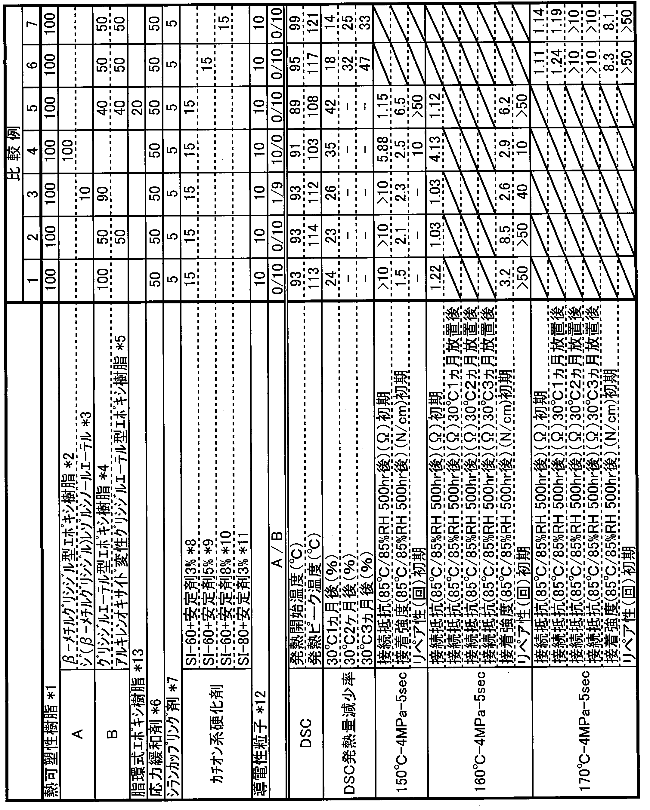
表1からわかるように、実施例1~12の異方性導電フィルムは、エポキシ樹脂として、通常のグリシジルエーテル型エポキシ樹脂とβ-アルキルグリシジル型エポキシ樹脂とを、質量比9:1~2:8の割合で含有しているので、DSCの発熱開始温度や発熱ピーク温度に問題はなく、しかも低温速硬化性が改善され、しかもリペア性、接続信頼性及び保存安定性についても同時に改善された。
それに対し、表2の比較例1の異方性導電フィルムは、エポキシ樹脂として、β-アルキルグリシジル型エポキシ樹脂を使用せずに、通常のグリシジルエーテル型エポキシ樹脂のみを使用したため、150℃-4MPa-5秒という比較的低温の熱圧着条件における初期接続抵抗並びに接着強度に問題があった。また、160℃-4MPa-5秒という熱圧着条件でも、接着強度とリペア性とに問題があった。
また、比較例2の異方性導電フィルムは、β-アルキルグリシジル型エポキシ樹脂を使用せずに、比較例1に比べ、エポキシ樹脂として、通常のグリシジルエーテル型エポキシ樹脂の半分をアルキレンオキサイド変性グリシジルエーテル型エポキシ樹脂に代替させたものの、結局のところグリシジルエーテル型エポキシ樹脂のみを使用したものに過ぎないため、比較例1と同様に、150℃-4MPa-5秒という比較的低温の熱圧着条件における初期接続抵抗並びに接着強度に問題があり、また、160℃-4MPa-5秒という熱圧着条件でもリペア性に問題があった。
比較例3の異方性導電フィルムは、エポキシ樹脂として、β-アルキルグリシジル型エポキシ樹脂とグリシジルエーテル型エポキシ樹脂とを併用しているものの、質量比が1:9の割合であるため、150℃-4MPa-5秒という比較的低温の熱圧着条件における初期接続抵抗並びに接着強度に問題があった。また、160℃-4MPa-5秒という熱圧着条件でも接着強度とリペア性とに問題があった。
比較例4の異方性導電フィルムは、エポキシ樹脂として、β-アルキルグリシジル型エポキシ樹脂のみを使用したため、150℃-4MPa-5秒という比較的低温の熱圧着条件におけるリペア性に問題はなかったが、初期接続抵抗並びに接着強度に問題があり、また、160℃-4MPa-5秒という熱圧着条件でも接着強度に問題があった。
比較例5の異方性導電フィルムは、比較例2に比べ、エポキシ樹脂として、通常のグリシジルエーテル型エポキシ樹脂及びアルキレンオキサイド変性グリシジルエーテル型エポキシ樹脂のそれぞれ一部を脂環式エポキシ樹脂に代えているものの、β-アルキルグリシジル型エポキシ樹脂を使用していないため、DSCの反応開始温度が低く、また、150℃並びに160℃-4MPa-5秒という比較的低温並びに中温の熱圧着条件におけるリペア性に問題があった。
比較例6及び7の異方性導電フィルムは、比較例2に比べ、カチオン系硬化剤中の安定剤量を3%からそれぞれ5%及び8%に増量したものであるが、エポキシ樹脂として、比較例2と同様に、β-アルキルグリシジル型エポキシ樹脂を使用せずに、通常のグリシジルエーテル型エポキシ樹脂とアルキレンオキサイド変性グリシジルエーテル型エポキシ樹脂とを使用したので、170℃-4MPa-5秒という熱圧着条件におけるリペア性に問題があった。
カチオン系硬化剤を使用する本発明のエポキシ樹脂ベースの異方性導電フィルムは、導電性粒子の分散媒となる熱硬化型エポキシ樹脂組成物を構成するエポキシ樹脂として、β-アルキルグリシジル型エポキシ樹脂をグリシジルエーテル型エポキシ樹脂と所定割合で併用するので、低温速硬化性、リペア性、接続信頼性及び保存安定性について同時に改善できる。従って、半導体装置やLED装置等の製造に有用である。
10 第1の電子部品
11、31 端子
20 異方性導電フィルム
21 導電性粒子
30 第2の電子部品
40 加熱ボンダー
100 接続構造体
11、31 端子
20 異方性導電フィルム
21 導電性粒子
30 第2の電子部品
40 加熱ボンダー
100 接続構造体
Claims (7)
- エポキシ樹脂と、エポキシ樹脂用硬化剤としてカチオン系硬化剤と、膜形成用樹脂とを含む熱硬化型エポキシ樹脂組成物中に導電性粒子が分散している異方性導電フィルムにおいて、
該エポキシ樹脂が、β-アルキルグリシジル型エポキシ樹脂とグリシジルエーテル型エポキシ樹脂とを質量比9:1~2:8の割合で含有する異方性導電フィルム。 - 該エポキシ樹脂が、β-アルキルグリシジル型エポキシ樹脂とグリシジルエーテル型エポキシ樹脂とを質量比8:2~4:6の割合で含有する請求項1記載の異方性導電フィルム。
- 該β-アルキルグリシジル型エポキシ樹脂が、ジ(β-メチルグリシジル)レゾルシノールエーテルである請求項1又は2記載の異方性導電フィルム。
- 該グリシジルエーテル型エポキシ樹脂が、アルキレンオキサイド変性グリシジルエーテル型エポキシ樹脂である請求項1~3のいずれかに記載の異方性導電フィルム。
- カチオン系硬化剤が、アリールスルホニウム塩系硬化剤である請求項1~4のいずれかに記載の異方性導電フィルム。
- 第1の電子部品の端子と第2の電子部品の端子とが異方性導電フィルムにより異方性導電接続されている接続構造体の製造方法であって、
第1の電子部品の端子上に、請求項1~5のいずれかに記載の異方性導電フィルムを仮貼りする工程、
仮貼りされた異方性導電フィルム上に、第2の電子部品を、その端子が第1の電子部品の対応する端子と対向するように仮設置する工程、及び
第2の電子部品を加熱ボンダーで加熱しながら第1の電子部品に対して押圧し、第1の電子部品の端子と第2の電子部品の端子とを異方性導電接続する工程
を有する製造方法。 - 第1の電子部品の端子と第2の電子部品の端子とが請求項1~5のいずれかに記載の異方性導電フィルムにより異方性導電接続されてなる接続構造体。
Priority Applications (2)
| Application Number | Priority Date | Filing Date | Title |
|---|---|---|---|
| CN201280018363.7A CN103459453B (zh) | 2011-04-14 | 2012-04-02 | 各向异性导电膜 |
| KR1020137026377A KR20140019363A (ko) | 2011-04-14 | 2012-04-02 | 이방성 도전 필름 |
Applications Claiming Priority (2)
| Application Number | Priority Date | Filing Date | Title |
|---|---|---|---|
| JP2011090211A JP5768454B2 (ja) | 2011-04-14 | 2011-04-14 | 異方性導電フィルム |
| JP2011-090211 | 2011-04-14 |
Publications (1)
| Publication Number | Publication Date |
|---|---|
| WO2012141027A1 true WO2012141027A1 (ja) | 2012-10-18 |
Family
ID=47009206
Family Applications (1)
| Application Number | Title | Priority Date | Filing Date |
|---|---|---|---|
| PCT/JP2012/058917 Ceased WO2012141027A1 (ja) | 2011-04-14 | 2012-04-02 | 異方性導電フィルム |
Country Status (4)
| Country | Link |
|---|---|
| JP (1) | JP5768454B2 (ja) |
| KR (1) | KR20140019363A (ja) |
| CN (1) | CN103459453B (ja) |
| WO (1) | WO2012141027A1 (ja) |
Cited By (2)
| Publication number | Priority date | Publication date | Assignee | Title |
|---|---|---|---|---|
| CN108140452A (zh) * | 2015-09-30 | 2018-06-08 | 三星Sdi株式会社 | 各向异性导电膜和使用其的显示设备 |
| TWI781710B (zh) * | 2014-10-28 | 2022-10-21 | 日商迪睿合股份有限公司 | 異向性導電膜、其製造方法及連接構造體 |
Families Citing this family (13)
| Publication number | Priority date | Publication date | Assignee | Title |
|---|---|---|---|---|
| JP6007022B2 (ja) * | 2012-08-06 | 2016-10-12 | デクセリアルズ株式会社 | 回路接続材料 |
| KR20150092077A (ko) * | 2012-12-06 | 2015-08-12 | 세키스이가가쿠 고교가부시키가이샤 | 도전 재료, 접속 구조체 및 접속 구조체의 제조 방법 |
| JP6180159B2 (ja) | 2013-04-04 | 2017-08-16 | デクセリアルズ株式会社 | 異方性導電フィルム、接続方法、及び接合体 |
| KR101706818B1 (ko) | 2014-04-30 | 2017-02-15 | 제일모직주식회사 | 이방 도전성 필름용 조성물, 이방 도전성 필름 및 반도체 장치 |
| KR101712703B1 (ko) * | 2014-07-18 | 2017-03-06 | 삼성에스디아이 주식회사 | 접착 조성물, 이방 도전성 필름 및 이를 이용한 반도체 장치 |
| KR101706821B1 (ko) | 2014-09-01 | 2017-02-14 | 삼성에스디아이 주식회사 | 이방 도전성 필름 및 상기 필름에 의해 접속된 반도체 장치 |
| JP2016089153A (ja) * | 2014-10-29 | 2016-05-23 | デクセリアルズ株式会社 | 導電材料 |
| KR101900542B1 (ko) * | 2015-09-30 | 2018-09-19 | 삼성에스디아이 주식회사 | 이방 도전성 필름용 조성물, 이방 도전성 필름 및 이를 이용한 디스플레이 장치 |
| JP6672837B2 (ja) * | 2016-01-28 | 2020-03-25 | 日立化成株式会社 | 異方導電性接着剤組成物、フィルム状接着剤、接続構造体及び半導体装置 |
| JP2018104653A (ja) * | 2016-12-28 | 2018-07-05 | 日立化成株式会社 | 接着剤組成物の選別方法、回路部材の接続方法、接続構造体、接着剤組成物及びフィルム状接着剤 |
| CN107248539B (zh) * | 2017-04-28 | 2020-02-07 | 厦门市三安光电科技有限公司 | 一种led封装工艺 |
| JP6956190B2 (ja) * | 2017-08-29 | 2021-11-02 | 三菱重工業株式会社 | 硬化性組成物、硬化性ペースト材、硬化性シート材、硬化性型取り材、硬化方法および硬化物 |
| JP2025079110A (ja) * | 2023-11-09 | 2025-05-21 | 株式会社レゾナック | 回路接続構造体の製造方法、回路接続用接着剤フィルム、及び回路接続構造体 |
Citations (4)
| Publication number | Priority date | Publication date | Assignee | Title |
|---|---|---|---|---|
| JP2005307031A (ja) * | 2004-04-22 | 2005-11-04 | Dainippon Ink & Chem Inc | エポキシ樹脂組成物及びその硬化物 |
| JP2006137825A (ja) * | 2004-11-11 | 2006-06-01 | Dainippon Ink & Chem Inc | 1液型エポキシ樹脂組成物及びその硬化物 |
| JP2007269979A (ja) * | 2006-03-31 | 2007-10-18 | Dainippon Ink & Chem Inc | エポキシ樹脂組成物、その硬化物、半導体封止材料、および半導体装置 |
| JP2010278025A (ja) * | 2010-08-30 | 2010-12-09 | Sony Chemical & Information Device Corp | 異方性導電フィルム |
Family Cites Families (1)
| Publication number | Priority date | Publication date | Assignee | Title |
|---|---|---|---|---|
| CN101465408B (zh) * | 2008-12-31 | 2010-12-29 | 电子科技大学 | 一种柔性有机光电子器件用基板及其制备方法 |
-
2011
- 2011-04-14 JP JP2011090211A patent/JP5768454B2/ja active Active
-
2012
- 2012-04-02 CN CN201280018363.7A patent/CN103459453B/zh not_active Expired - Fee Related
- 2012-04-02 WO PCT/JP2012/058917 patent/WO2012141027A1/ja not_active Ceased
- 2012-04-02 KR KR1020137026377A patent/KR20140019363A/ko not_active Withdrawn
Patent Citations (4)
| Publication number | Priority date | Publication date | Assignee | Title |
|---|---|---|---|---|
| JP2005307031A (ja) * | 2004-04-22 | 2005-11-04 | Dainippon Ink & Chem Inc | エポキシ樹脂組成物及びその硬化物 |
| JP2006137825A (ja) * | 2004-11-11 | 2006-06-01 | Dainippon Ink & Chem Inc | 1液型エポキシ樹脂組成物及びその硬化物 |
| JP2007269979A (ja) * | 2006-03-31 | 2007-10-18 | Dainippon Ink & Chem Inc | エポキシ樹脂組成物、その硬化物、半導体封止材料、および半導体装置 |
| JP2010278025A (ja) * | 2010-08-30 | 2010-12-09 | Sony Chemical & Information Device Corp | 異方性導電フィルム |
Cited By (3)
| Publication number | Priority date | Publication date | Assignee | Title |
|---|---|---|---|---|
| TWI781710B (zh) * | 2014-10-28 | 2022-10-21 | 日商迪睿合股份有限公司 | 異向性導電膜、其製造方法及連接構造體 |
| CN108140452A (zh) * | 2015-09-30 | 2018-06-08 | 三星Sdi株式会社 | 各向异性导电膜和使用其的显示设备 |
| CN108140452B (zh) * | 2015-09-30 | 2020-02-18 | 国都化学株式会社 | 各向异性导电膜和使用其的显示设备 |
Also Published As
| Publication number | Publication date |
|---|---|
| KR20140019363A (ko) | 2014-02-14 |
| CN103459453A (zh) | 2013-12-18 |
| JP5768454B2 (ja) | 2015-08-26 |
| CN103459453B (zh) | 2016-02-10 |
| JP2012219262A (ja) | 2012-11-12 |
Similar Documents
| Publication | Publication Date | Title |
|---|---|---|
| JP5768454B2 (ja) | 異方性導電フィルム | |
| JP5186157B2 (ja) | 異方性導電フィルム及びそれを用いた接続構造体の製造方法 | |
| JP4962156B2 (ja) | 導電性接着剤 | |
| KR20120130705A (ko) | 실페닐렌 구조 및 실록산 구조를 갖는 중합체 및 이의 제조 방법, 접착제 조성물, 접착 시트 및 반도체 장치 보호용 재료, 및 반도체 장치 | |
| JP2001207150A (ja) | 接着剤組成物 | |
| WO2016194952A1 (ja) | 接着剤組成物 | |
| JP2017132919A (ja) | 異方導電性接着剤組成物、フィルム状接着剤、接続構造体及び半導体装置 | |
| KR102036570B1 (ko) | 회로 접속 재료 및 이것을 사용한 실장체의 제조 방법 | |
| KR102098758B1 (ko) | 회로 접속 재료 | |
| JPWO2018181536A1 (ja) | 接着剤組成物及び構造体 | |
| CN102153957A (zh) | 粘接膜、以及电路部件的连接结构和连接方法 | |
| TWI476267B (zh) | Anisotropic conductive adhesive | |
| JP3947532B2 (ja) | 異方導電性接着剤フィルム | |
| JP6181825B2 (ja) | 異方性導電フィルム、及びこれを用いた実装体の製造方法 | |
| CN107851478B (zh) | 非等向性导电膜用组成物、非等向性导电膜及使用其的显示装置 | |
| JP5258191B2 (ja) | 半導体チップ接合用接着剤 | |
| CN117659667B (zh) | 热固化型树脂组合物、各向异性导电膜及连接结构体 | |
| JP2005175338A (ja) | 半導体用接着フィルムおよび半導体装置 | |
| TWI623569B (zh) | 各向異性導電膜和使用其的顯示裝置 | |
| JP4730215B2 (ja) | 異方導電性接着剤フィルム | |
| JP6472702B2 (ja) | 異方性導電フィルム、接続方法、及び接合体 | |
| TWI663608B (zh) | 導電性樹脂組合物及半導體裝置 | |
| HK1188802A (en) | Anisotropic conductive film | |
| CN118978884A (zh) | 一种组合物及其应用 | |
| KR100727550B1 (ko) | 반도체 장치용 접착제 조성물 및 반도체 장치용 접착시트 |
Legal Events
| Date | Code | Title | Description |
|---|---|---|---|
| 121 | Ep: the epo has been informed by wipo that ep was designated in this application |
Ref document number: 12770682 Country of ref document: EP Kind code of ref document: A1 |
|
| ENP | Entry into the national phase |
Ref document number: 20137026377 Country of ref document: KR Kind code of ref document: A |
|
| NENP | Non-entry into the national phase |
Ref country code: DE |
|
| 122 | Ep: pct application non-entry in european phase |
Ref document number: 12770682 Country of ref document: EP Kind code of ref document: A1 |