WO2012137546A1 - パワースイッチのウェハ試験方法 - Google Patents
パワースイッチのウェハ試験方法 Download PDFInfo
- Publication number
- WO2012137546A1 WO2012137546A1 PCT/JP2012/053786 JP2012053786W WO2012137546A1 WO 2012137546 A1 WO2012137546 A1 WO 2012137546A1 JP 2012053786 W JP2012053786 W JP 2012053786W WO 2012137546 A1 WO2012137546 A1 WO 2012137546A1
- Authority
- WO
- WIPO (PCT)
- Prior art keywords
- current
- igbt
- terminal
- main
- detection
- Prior art date
- Legal status (The legal status is an assumption and is not a legal conclusion. Google has not performed a legal analysis and makes no representation as to the accuracy of the status listed.)
- Ceased
Links
Images



Classifications
-
- G—PHYSICS
- G01—MEASURING; TESTING
- G01R—MEASURING ELECTRIC VARIABLES; MEASURING MAGNETIC VARIABLES
- G01R31/00—Arrangements for testing electric properties; Arrangements for locating electric faults; Arrangements for electrical testing characterised by what is being tested not provided for elsewhere
- G01R31/26—Testing of individual semiconductor devices
- G01R31/2607—Circuits therefor
- G01R31/2608—Circuits therefor for testing bipolar transistors
-
- H—ELECTRICITY
- H10—SEMICONDUCTOR DEVICES; ELECTRIC SOLID-STATE DEVICES NOT OTHERWISE PROVIDED FOR
- H10P—GENERIC PROCESSES OR APPARATUS FOR THE MANUFACTURE OR TREATMENT OF DEVICES COVERED BY CLASS H10
- H10P74/00—Testing or measuring during manufacture or treatment of wafers, substrates or devices
- H10P74/20—Testing or measuring during manufacture or treatment of wafers, substrates or devices characterised by the properties tested or measured, e.g. structural or electrical properties
- H10P74/207—Electrical properties, e.g. testing or measuring of resistance, deep levels or capacitance-voltage characteristics
-
- H—ELECTRICITY
- H10—SEMICONDUCTOR DEVICES; ELECTRIC SOLID-STATE DEVICES NOT OTHERWISE PROVIDED FOR
- H10P—GENERIC PROCESSES OR APPARATUS FOR THE MANUFACTURE OR TREATMENT OF DEVICES COVERED BY CLASS H10
- H10P74/00—Testing or measuring during manufacture or treatment of wafers, substrates or devices
- H10P74/27—Structural arrangements therefor
- H10P74/277—Circuits for electrically characterising or monitoring manufacturing processes, e.g. circuits in tested chips or circuits in testing wafers
Definitions
- the present invention relates to a wafer test method for a power switch integrated and formed on a semiconductor substrate.
- a power switch integrated and formed on a semiconductor substrate is used in, for example, an internal combustion engine ignition system of an automobile.
- FIG. 4 shows a configuration example of an internal combustion engine ignition system using a power switch.
- the internal combustion engine ignition system shown in FIG. 4 includes a power switch 11, an engine control unit (hereinafter referred to as ECU (Electronic Control Unit)) 15, a battery power supply 16, an ignition coil 17, and a spark plug 18. It is configured.
- ECU Engine Control Unit
- the primary current flowing through the primary side coil of the ignition coil 17 connected to the battery power source 16 is controlled by the power switch 11 to turn on (conduct) and off (shut off), thereby inducing a high voltage in the secondary side coil and igniting.
- a spark discharge is generated by the plug 18.
- the on / off of the power switch 11 is controlled by an on / off signal from the ECU 15.
- the power switch 11 shown in FIG. 4 includes a power switch unit 10 and a control unit 14, and is connected to a collector terminal (hereinafter referred to as a C terminal) 4 that is connected to the primary coil of the ignition coil 17 and the ECU 15. It has a gate terminal 8 and an emitter terminal 9 connected to a ground potential (hereinafter referred to as GND).
- the power switch unit 10 includes a main IGBT (Insulated Gate Bipolar Transistor) 1, a current detection IGBT 2, and a gate resistance circuit 3.
- a control unit 14 includes a current detection circuit 12, a gate drive circuit 13, Consists of
- the power switch 11 shown in FIG. 4 is formed on a separate semiconductor substrate in the case of a one-chip configuration in which the power switch unit 10 and the control unit 14 are integrated on the same semiconductor substrate. There is a case of a two-chip configuration.
- a gate terminal (hereinafter referred to as G terminal) 5 an emitter terminal (hereinafter referred to as E1 terminal) 6 of the main IGBT 1, and current detection, which are connection points between the power switch unit 10 and the control unit 14.
- the connection points of the emitter terminal (hereinafter referred to as E2 terminal) 7 of the IGBT 2 for use are connected by connecting means such as wire bonding.
- the G terminal 5, the E1 terminal 6, and the E2 terminal 7 that are connection points between the power switch unit 10 and the control unit 14 are used as measurement test terminals during the wafer test, respectively.
- the power switch 11 shown in FIG. 4 is provided with a current limiting function for limiting the primary current for the purpose of preventing the ignition coil 17 from being burned out due to the overcurrent of the primary current and ensuring the spark discharge stability at the start.
- the current limiting function includes means for detecting the primary current by the current detection IGBT 2 and the current detection circuit 12, and the gate drive circuit 13 and the gate resistance circuit 3 according to the detection result of the primary current by the gates of the main IGBT 1 and the current detection IGBT 2. This is realized by means for controlling the voltage.
- the primary current that flows through the primary coil of the ignition coil 17 is the main current that flows from the C terminal 4 of the power switch unit 10 to the E1 terminal 6 and the emitter terminal 9 of the main IGBT 1 and the C terminal of the power switch unit 10. 4 and the detection current flowing through the path of the E2 terminal 7 of the current detection IGBT 2, the current detection circuit 12, and the emitter terminal 9.
- the current ratio (main current flowing in the main IGBT 1 / detected current flowing in the current detecting IGBT 2) is normally set to 100 or more.
- Patent Document 1 discloses a technique for adjusting the reference voltage of the current control unit based on the measurement results of the main current and the detected current in order to match the current ratio (main current / detected current), which is an important characteristic, with the design value. It is disclosed.
- the power switch 11 includes the power switch unit 10 and the control unit 14 and is configured by one chip or two chips.
- the power switch 11 omits the control unit 14 (it is an irrelevant function when measuring the current ratio), and only the power switch unit 10 is explicitly described.
- FIG. 5 is a wafer test circuit for measuring the main current flowing through the main IGBT 1 of the power switch unit 10 in the power switch 11 and is composed of the power switch unit 10, the tester 20, and the tester prober 21.
- the tester prober 21 has a tester prober stage 22 for setting the test wafer of the power switch unit 10 and a probe card 23 for connecting each measurement terminal of the tester 20 to each terminal of the test wafer of the power switch unit 10. Yes.
- the EV_t terminal of the tester 20 is connected to the EV_p terminal of the probe card 23, and the E1 terminal (pad) 6 on the wafer of the power switch unit 10 is connected with the probe connected to the EV_p terminal of the probe card 23.
- the E1 terminal 6 is set to a reference potential (usually GND).
- the GV_t terminal of the tester 20 is connected to the GV_p terminal of the probe card 23, and the G terminal (pad) on the wafer of the power switch unit 10 is connected with the probe connected to the GV_p terminal of the probe card 23. 5 and a constant voltage Vo (V) that turns on the main IGBT 1 is applied.
- the CI_t terminal of the tester 20 is connected to the stage 22 of the tester prober (CI_s is added as a terminal name), and is connected to the C terminal 4 on the back surface of the wafer of the power switch unit 10 (the back surface electrode of the wafer).
- CI_s is added as a terminal name
- the C terminal 4 Corresponds to the C terminal 4
- a constant current Io (A) is applied to the main IGBT1.
- the main current Im (A) flowing through the main IGBT 1 is measured by connecting the current flowing through the E1 terminal 6 to the EI_t terminal of the tester 20 via the EI_p terminal of the probe card 23.
- FIG. 6 is a wafer test circuit for measuring the detection current flowing through the current detection IGBT 2 of the power switch unit 10 in the power switch 11, and as in FIG. 5, the power switch unit 10, the tester 20, and the tester prober. 21.
- the tester prober 21 has a tester prober stage 22 for setting the test wafer of the power switch unit 10 and a probe card 23 for connecting each measurement terminal of the tester 20 to each terminal of the test wafer of the power switch unit 10. Yes.
- the EV_t terminal of the tester 20 is connected to the EV_p terminal of the probe card 23, and the E2 terminal (pad) 7 on the wafer of the power switch unit 10 is connected with the probe connected to the EV_p terminal of the probe card 23. And the E2 terminal 7 is set to a reference potential (usually GND).
- the GV_t terminal of the tester 20 is connected to the GV_p terminal of the probe card 23, and the G terminal (pad) on the wafer of the power switch unit 10 is connected with the probe connected to the GV_p terminal of the probe card 23.
- the CI_t terminal of the tester 20 is connected to the C terminal 4 on the back surface of the wafer of the power switch unit 10 through the stage 22 of the tester prober (the terminal name is CI_s) (the back surface electrode of the wafer is connected). This corresponds to the C terminal 4), and a constant current Io (A) is applied to the current detection IGBT 2.
- the current flowing through the E2 terminal 7 is connected to the EI_t terminal of the tester 20 via the EI_p terminal of the probe card 23, and the detection current Is (A) flowing through the current detection IGBT 2 is measured.
- the current ratio (main current / detected current) of the power switch unit 10 in the power switch 11 is obtained by calculating Im (A) / detected current Is (A).
- the current ratio (main current / detection current) is determined by the layout area ratio on the semiconductor substrate.
- the main IGBT 1 and the current detection IGBT 2 are simultaneously turned on / off, and therefore the positional relationship (distance) of the layout arrangement of the main IGBT 1 and the current detection IGBT 2 on the semiconductor substrate.
- the current ratio (main current / detection current) cannot be measured accurately.
- the current detection circuit 12 of the power switch 11 shown in FIG. 4 includes a sense resistor Rsns (detected by converting the current into a voltage) for detecting the detection current flowing through the current detection IGBT 2. Yes. For this reason, in the actual operation state of the power switch 11, between the G terminal 5, the E1 terminal 6, and the E2 terminal 7 of the main IGBT 1 of the power switch unit 10 and the current detection IGBT 2 by the voltage generated by the sense resistor Rsns. A voltage difference is generated between the voltage and the voltage between the C terminal 4 and the E1 terminal 6 and E2 terminal 7. However, since this voltage difference is not considered in the conventional wafer test method described with reference to FIGS. 5 and 6, the current ratio (main current / detected current) cannot be accurately measured.
- a sense resistor Rsns detected by converting the current into a voltage
- the present invention has been made in view of the above-described problems, and the problem to be solved is that the main IGBT, the collector terminal and the gate terminal are connected to the collector terminal and the gate terminal of the main IGBT, respectively.
- a current ratio between a main current flowing through the main IGBT and a detection current flowing through the current detection IGBT main current / detection current
- a wafer test method for a power switch includes connecting a resistor between a main IGBT emitter terminal pin and a current detection IGBT emitter terminal pin of a probe card used for a wafer test, A voltage difference is provided between the emitter terminal of the main IGBT and the emitter terminal of the current detection IGBT, and the wafer test is performed with the main IGBT and the current detection IGBT turned on at the same time. / Detection current).
- the wafer test method for a power switch includes a main IGBT and a current detection IGBT in which a collector terminal and a gate terminal are connected to a collector terminal and a gate terminal of the main IGBT, respectively, and a current value of the main IGBT is detected.
- a wafer test method for a power switch in which the main IGBT and the current detection IGBT are integrated on the same semiconductor substrate, wherein the emitter current of the current detection IGBT is the emitter of the main IGBT.
- a resistance means is provided to flow through the terminal, the main IGBT and the current detection IGBT are simultaneously conducted to apply a constant current to the common collector terminal of the main IGBT and the current detection IGBT, and the voltage is obtained from the voltage across the resistance means. From the current flowing through the current detection IGBT and the constant current, the main current of the main IGBT And calculating the current ratio of the detected current of the current detecting IGBT (the main current / detection current).
- the power switch wafer testing method includes a main IGBT and a current detection IGBT in which a collector terminal and a gate terminal are connected to a collector terminal and a gate terminal of the main IGBT, respectively, and a current value of the main IGBT is detected. And a wafer test method for a power switch in which the main IGBT and the current detection IGBT are integrated on the same semiconductor substrate, wherein the emitter current of the current detection IGBT is the emitter of the main IGBT.
- a resistance means is provided to flow through the terminal, and the main IGBT and the current detection IGBT are simultaneously conducted to detect a sum current of the main current of the main IGBT and the detection current of the current detection IGBT flowing from the emitter terminal of the main IGBT. And detecting the detection current of the current detecting IGBT from the voltage across the resistance means. , And calculates the current ratio of the detected current of the main current and the current detecting IGBT of the main IGBT (main current / detection current).
- the resistance means is connected between terminals of a wafer test probe card corresponding to the emitter terminal of the main IGBT and the emitter terminal of the current detection IGBT.
- a resistor is connected between the emitter terminal pin of the main IGBT of the probe card for wafer measurement and the emitter terminal pin of the current detection IGBT, and the emitter terminal of the main IGBT and the current are connected.
- the power switch according to the present invention is used in, for example, an internal combustion engine ignition system.
- the configuration example of the internal combustion engine ignition system is the same as that of FIG. 4 described above, and detailed description thereof is omitted.
- the configuration of the power switch according to the present invention is the same as that of FIG. 4 described above. That is, the power switch 11 includes a power switch unit 10 including a main IGBT 1, a current detection IGBT 2, and a gate resistor circuit 3, a current detection circuit 12, and a control unit 14 including a gate drive circuit 13. Consists of The power switch 11 has a C terminal 4 connected to the primary coil of the ignition coil 17, a gate terminal 8 connected to the ECU 15, and an emitter terminal 9 connected to GND.
- the power switch 11 has a single-chip configuration in which the power switch unit 10 and the control unit 14 are integrally formed on the same semiconductor substrate, and a separate semiconductor substrate. There is a case of a two-chip configuration to be formed.
- the G terminal 5, the E1 terminal 6 and the E2 terminal 7 which are connection points between the power switch unit 10 and the control unit 14 are respectively connected by connection means such as wire bonding in the case of a two-chip configuration, and in the case of a one-chip configuration. Used as a test terminal for measurement during a wafer test.
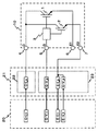
- FIG. 1 is a configuration example of a wafer test circuit used in a wafer test method of a current ratio of the power switch 11 according to the present invention (main current flowing in the main IGBT 1 / detected current flowing in the current detecting IGBT 2).
- the power switch unit 10 and the control unit 14 are configured by one chip or two chips.
- the power switch 11 is the control unit. 14 is omitted (this is an irrelevant function when measuring the current ratio), and only the power switch unit 10 is clearly shown.
- the same parts as those in FIGS. 5 and 6 described in the conventional power switch wafer test method are denoted by the same reference numerals, and detailed description thereof is omitted.
- FIG. 1 shows a wafer test circuit for measuring the current ratio (main current / detected current) of the power switch 11, and is composed of a power switch unit 10, a tester 20, and a tester prober 21.
- the tester prober 21 includes a tester prober stage 22 for setting a test wafer of the power switch unit 10 and a probe card 23 for connecting each measurement terminal of the tester 20 to each terminal of the test wafer of the power switch unit 10.
- a resistor R is installed on the probe card 23.
- the tester 20 includes terminals CI_t, CV_t, GV_t, EI_t, EV_t, and SV_t for applying or measuring a current or voltage.
- the probe card 23 includes terminals GV_p, EI_p, EV_p, and SV_p corresponding to the terminals of the tester 20.
- Each terminal of the probe card 23 has a probe and is connected to the G terminal 5, the E1 terminal 6, and the E2 terminal 7 which are pads on the wafer of the power switch unit 10.
- a resistor R is connected between the EV_p terminal and the SV_p terminal on the probe card 23. The resistor R sets a voltage difference between the E1 terminal 6 of the main IGBT 1 and the E2 terminal 7 of the current detection IGBT 2.
- the stage 22 of the tester prober is labeled with the CI_s terminal and the CV_s terminal corresponding to the CI_t terminal and the CV_t terminal of the tester 20.
- C terminal 4 (the back electrode of the wafer corresponds to C terminal 4) is connected.
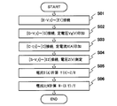
- FIG. 2 is a test flowchart showing the procedure of the first wafer test method related to the wafer test method of the power switch 11 according to the present invention.
- step S01 the EV_t terminal of the tester 20 is connected to the EV_p terminal of the probe card 23, and the power switch unit 10 is connected with the probe connected to the EV_p terminal of the probe card 23.
- the E1 terminal (pad) 6 on the wafer To the E1 terminal (pad) 6 on the wafer, and the E1 terminal 6 is set to a reference potential.
- step S02 the GV_t terminal of the tester 20 is connected to the GV_p terminal of the probe card 23, and the G terminal on the wafer of the power switch unit 10 is connected with the probe connected to the GV_p terminal of the probe card 23.
- a constant voltage Vg (V) is applied so that the main IGBT 1 and the current detection IGBT 2 are simultaneously turned on.
- step S03 the CI_t terminal of the tester 20 is connected to the C terminal 4 on the back surface of the wafer of the power switch unit 10 through the stage 22 (sign of the CI_s terminal) of the tester prober, and the main IGBT 1 and current detection A constant current X (A) is applied to the IGBT 2 for use.
- step S04 the SV_t terminal of the tester 20 is connected to the SV_p terminal of the probe card 23, and the E2 terminal on the wafer of the power switch unit 10 is connected with the probe connected to the SV_p terminal of the probe card 23.
- (Pad) 7 is connected, and the voltage Z (V) of the E2 terminal 7 of the current detection IGBT 2 is measured.
- the voltage Z (V) is divided into a main current flowing through the main IGBT 1 and a detection current flowing through the current detecting IGBT 2 when the constant current X (A) applied to the C terminal 4 is passed through the resistor R. This is the generated voltage. That is, the voltage Z (V) corresponds to a voltage difference generated by the resistance R between the E1 terminal 6 of the main IGBT 1 and the E2 terminal of the current detection IGBT 2 due to the constant current X (A) applied to the C terminal 4.
- the wafer test method for the power switch 11 is a power switch wafer test method in which the main IGBT 1 and the current detection IGBT 2 are integrated and formed on the same semiconductor substrate, and the main IGBT 1 A resistor R is connected between the EV_p terminal and the SV_p terminal of the wafer measurement probe card corresponding to the E1 terminal 6 of the current detection IGBT 2 and the E2 terminal 7 of the current detection IGBT 2.
- the current ratio of the primary current in the same state as the actual operation (Main current flowing through the main IGBT 1 / detected current flowing through the current detecting IGBT 2) can be measured easily and accurately.
- FIG. 3 is a test flowchart showing the procedure of the second wafer test method related to the wafer test method of the power switch 11 according to the present invention.
- step S11 the EV_t terminal of the tester 20 is connected to the EV_p terminal of the probe card 23, and the power switch unit 10 is connected with the probe connected to the EV_p terminal of the probe card 23.
- the E1 terminal (pad) 6 on the wafer To the E1 terminal (pad) 6 on the wafer, and the E1 terminal 6 is set to a reference potential.
- step S12 the GV_t terminal of the tester 20 is connected to the GV_p terminal of the probe card 23, and the G terminal on the wafer of the power switch unit 10 is connected with the probe connected to the GV_p terminal of the probe card 23.
- a constant voltage Vg (V) is applied so that the main IGBT 1 and the current detection IGBT 2 are simultaneously turned on.
- step S13 the CV_t terminal of the tester 20 is connected to the C terminal 4 on the back surface of the wafer of the power switch unit 10 through the stage 22 (reference number of the CV_s terminal) of the tester prober, and the main IGBT 1 and current detection are performed.
- a constant voltage Vc (V) is applied to the IGBT 2 for use.
- step S14 the SV_t terminal of the tester 20 is connected to the SV_p terminal of the probe card 23, and the E2 terminal on the wafer of the power switch unit 10 is connected with the probe connected to the SV_p terminal of the probe card 23.
- (Pad) 7 is connected, and the voltage Z (V) of the E2 terminal 7 of the current detection IGBT 2 is measured.
- This voltage Z (V) is generated by the constant current Vc (V) applied to the C terminal 4, the main current flows through the main IGBT 1, the detection current flows through the current detection IGBT 2, and this detection current flows through the resistor R.
- Voltage That is, the voltage Z (V) corresponds to a voltage difference generated by the resistance R between the E1 terminal 6 of the main IGBT 1 and the E2 terminal of the current detection IGBT 2 due to the constant voltage Vc (V) applied to the C terminal 4.
- step S15 the EI_t terminal of the tester 20 is connected to the EI_p terminal of the probe card 23, and the main current and current detection that have flowed to the main IGBT 1 by the constant voltage Vc (V) applied to the C terminal 4 are detected.
- the sum current T (A) obtained by adding the detected current flowing through the IGBT 2 is measured.
- the wafer test method for the power switch 11 is a power switch wafer test method in which the main IGBT 1 and the current detection IGBT 2 are integrated and formed on the same semiconductor substrate, and the main IGBT 1 A resistor R is connected between the EV_p terminal and the SV_p terminal of the wafer measurement probe card corresponding to the E1 terminal 6 of the current detection IGBT 2 and the E2 terminal 7 of the current detection IGBT 2.
- the current ratio of the primary current in the same state as the actual operation (Main current flowing through the main IGBT 1 / detected current flowing through the current detecting IGBT 2) can be measured easily and accurately.
- the current ratio (main current / detected current) of the primary current in the wafer test of the power switch according to the present invention is the conventional wafer test method shown in FIGS.
- the wafer test method according to the present invention shown in FIG. 1 shows the same result as the measurement value of the product assembled in the package. Has been obtained.
Landscapes
- Engineering & Computer Science (AREA)
- Microelectronics & Electronic Packaging (AREA)
- Physics & Mathematics (AREA)
- General Physics & Mathematics (AREA)
- Testing Or Measuring Of Semiconductors Or The Like (AREA)
- Testing Of Individual Semiconductor Devices (AREA)
- Semiconductor Integrated Circuits (AREA)
Abstract
Description
上記については単に本発明の原理を示すものである。更に、多数の変形、変更が当業者にとって可能であり、本発明は上記に示し、説明した正確な構成および応用例に限定されるものではなく、対応するすべての変形例および均等物は、添付の請求項およびその均等物による本発明の範囲とみなされる。
2 電流検出用IGBT
3 ゲート抵抗回路
4 コレクタ端子(C端子)
5 ゲート端子(G端子)
6 主IGBT1のエミッタ端子(E1端子)
7 電流検出用IGBT2のエミッタ端子(E2端子)
8 ゲート端子
9 エミッタ端子(GND端子)
10 パワースイッチ部
11 パワースイッチ
12 電流検出回路
13 ゲート駆動回路
14 制御部
15 エンジンコントロールユニット(ECU)
16 バッテリー電源
17 点火コイル
18 点火プラグ
20 テスター
21 テスタープローバー
22 テスタープローバーのステージ
23 プローブカード
R 抵抗および抵抗値
Claims (4)
- 主IGBTと、コレクタ端子およびゲート端子がそれぞれ前記主IGBTのコレクタ端子およびゲート端子に接続されて前記主IGBTの電流値を検出する電流検出用IGBTと、を有し、前記主IGBTと前記電流検出用IGBTが同一の半導体基板上に集積形成されたパワースイッチのウェハ試験方法であって、
前記電流検出用IGBTのエミッタ電流を前記主IGBTのエミッタ端子に流す抵抗手段を設け、
前記主IGBTと前記電流検出用IGBTを同時に導通させて前記主IGBTと前記電流検出用IGBTの共通コレクタ端子に定電流を印加し、
前記抵抗手段の両端電圧から求めた前記電流検出用IGBTに流れる電流と、前記定電流とから、前記主IGBTの主電流と前記電流検出用IGBTの検出電流の電流比(主電流/検出電流)を算出することを特徴とするパワースイッチのウェハ試験方法。 - 前記抵抗手段は、前記主IGBTのエミッタ端子と前記電流検出用IGBTのエミッタ端子に対応するウェハ試験用プローブカードの端子間に接続されることを特徴とする請求の範囲第1項に記載のパワースイッチのウェハ試験方法。
- 主IGBTと、コレクタ端子およびゲート端子がそれぞれ前記主IGBTのコレクタ端子およびゲート端子に接続されて前記主IGBTの電流値を検出する電流検出用IGBTと、を有し、前記主IGBTと前記電流検出用IGBTが同一の半導体基板上に集積形成されたパワースイッチのウェハ試験方法であって、
前記電流検出用IGBTのエミッタ電流を前記主IGBTのエミッタ端子に流す抵抗手段を設け、
前記主IGBTと前記電流検出用IGBTを同時に導通させ、
前記主IGBTのエミッタ端子から流れる前記主IGBTの主電流と前記電流検出用IGBTの検出電流の和電流を検出するとともに、前記抵抗手段の両端電圧から前記電流検出用IGBTの検出電流を検出して、前記主IGBTの主電流と前記電流検出用IGBTの検出電流の電流比(主電流/検出電流)を算出することを特徴とするパワースイッチのウェハ試験方法。 - 前記抵抗手段は、前記主IGBTのエミッタ端子と前記電流検出用IGBTのエミッタ端子に対応するウェハ試験用プローブカードの端子間に接続されることを特徴とする請求の範囲第3項に記載のパワースイッチのウェハ試験方法。
Priority Applications (3)
| Application Number | Priority Date | Filing Date | Title |
|---|---|---|---|
| US14/009,347 US9541599B2 (en) | 2011-04-04 | 2012-02-17 | Power switch wafer test method |
| CN201280017290.XA CN103460367B (zh) | 2011-04-04 | 2012-02-17 | 功率开关的晶片测试方法 |
| JP2013508788A JP5720775B2 (ja) | 2011-04-04 | 2012-02-17 | パワースイッチのウェハ試験方法 |
Applications Claiming Priority (2)
| Application Number | Priority Date | Filing Date | Title |
|---|---|---|---|
| JP2011-082689 | 2011-04-04 | ||
| JP2011082689 | 2011-04-04 |
Publications (1)
| Publication Number | Publication Date |
|---|---|
| WO2012137546A1 true WO2012137546A1 (ja) | 2012-10-11 |
Family
ID=46968950
Family Applications (1)
| Application Number | Title | Priority Date | Filing Date |
|---|---|---|---|
| PCT/JP2012/053786 Ceased WO2012137546A1 (ja) | 2011-04-04 | 2012-02-17 | パワースイッチのウェハ試験方法 |
Country Status (4)
| Country | Link |
|---|---|
| US (1) | US9541599B2 (ja) |
| JP (1) | JP5720775B2 (ja) |
| CN (1) | CN103460367B (ja) |
| WO (1) | WO2012137546A1 (ja) |
Cited By (2)
| Publication number | Priority date | Publication date | Assignee | Title |
|---|---|---|---|---|
| CN104167374A (zh) * | 2013-05-17 | 2014-11-26 | 富士电机株式会社 | 半导体芯片的试验装置以及试验方法 |
| JP2019074043A (ja) * | 2017-10-17 | 2019-05-16 | 富士電機株式会社 | 半導体装置 |
Families Citing this family (5)
| Publication number | Priority date | Publication date | Assignee | Title |
|---|---|---|---|---|
| DE102016218662B4 (de) | 2016-09-28 | 2022-01-13 | Bayerische Motoren Werke Aktiengesellschaft | Testen einer elektrischen Fahrzeug-Komponente |
| PL234141B1 (pl) * | 2017-12-29 | 2020-01-31 | Akademia Morska W Gdyni | Sposób i układ do pomiaru własnych i wzajemnych rezystancji termicznych w module elektroizolowanym |
| DE102020103874B3 (de) * | 2020-02-14 | 2021-06-10 | Infineon Technologies Ag | Verfahren und schaltung zum überprüfen der funktionsfähigkeit eines transistorbauelements |
| KR102780349B1 (ko) | 2020-05-20 | 2025-03-12 | 삼성전자주식회사 | 프로브 카드 검사 장치 |
| JP7686521B2 (ja) * | 2021-09-24 | 2025-06-02 | 三菱電機株式会社 | 半導体装置 |
Citations (1)
| Publication number | Priority date | Publication date | Assignee | Title |
|---|---|---|---|---|
| JPH09233690A (ja) * | 1996-02-27 | 1997-09-05 | New Japan Radio Co Ltd | 出力電流制限回路及び出力電流制限回路における出力電流調整方法 |
Family Cites Families (8)
| Publication number | Priority date | Publication date | Assignee | Title |
|---|---|---|---|---|
| JPS5799789A (en) * | 1980-12-12 | 1982-06-21 | Seiko Instr & Electronics Ltd | Semiconductor thermo-sensitive element |
| JPH07161992A (ja) | 1993-10-14 | 1995-06-23 | Fuji Electric Co Ltd | 絶縁ゲート型バイポーラトランジスタ |
| JP3156487B2 (ja) | 1994-03-04 | 2001-04-16 | 富士電機株式会社 | 絶縁ゲート型バイポーラトランジスタ |
| FR2872645B1 (fr) * | 2004-07-02 | 2006-09-22 | Atmel Corp | Dispositif de conversion de puissance avec detecteur efficace de courant de sortie |
| US7336085B2 (en) * | 2006-02-17 | 2008-02-26 | Infineon Technologies Ag | Current sensing circuit |
| JP5010842B2 (ja) * | 2006-03-22 | 2012-08-29 | 東京エレクトロン株式会社 | 試験対象物の保護回路、試験対象物の保護方法、試験装置、及び試験方法 |
| JP2009165285A (ja) * | 2008-01-08 | 2009-07-23 | Panasonic Corp | 半導体装置 |
| DE112011102926B4 (de) * | 2010-09-03 | 2018-10-11 | Mitsubishi Electric Corp. | Halbleiterbauteil |
-
2012
- 2012-02-17 JP JP2013508788A patent/JP5720775B2/ja active Active
- 2012-02-17 WO PCT/JP2012/053786 patent/WO2012137546A1/ja not_active Ceased
- 2012-02-17 US US14/009,347 patent/US9541599B2/en active Active
- 2012-02-17 CN CN201280017290.XA patent/CN103460367B/zh active Active
Patent Citations (1)
| Publication number | Priority date | Publication date | Assignee | Title |
|---|---|---|---|---|
| JPH09233690A (ja) * | 1996-02-27 | 1997-09-05 | New Japan Radio Co Ltd | 出力電流制限回路及び出力電流制限回路における出力電流調整方法 |
Cited By (5)
| Publication number | Priority date | Publication date | Assignee | Title |
|---|---|---|---|---|
| CN104167374A (zh) * | 2013-05-17 | 2014-11-26 | 富士电机株式会社 | 半导体芯片的试验装置以及试验方法 |
| JP2014225607A (ja) * | 2013-05-17 | 2014-12-04 | 富士電機株式会社 | 半導体チップの試験装置および試験方法 |
| CN104167374B (zh) * | 2013-05-17 | 2018-05-01 | 富士电机株式会社 | 半导体芯片的试验装置以及试验方法 |
| JP2019074043A (ja) * | 2017-10-17 | 2019-05-16 | 富士電機株式会社 | 半導体装置 |
| JP7059564B2 (ja) | 2017-10-17 | 2022-04-26 | 富士電機株式会社 | 半導体装置 |
Also Published As
| Publication number | Publication date |
|---|---|
| JPWO2012137546A1 (ja) | 2014-07-28 |
| US20140035611A1 (en) | 2014-02-06 |
| JP5720775B2 (ja) | 2015-05-20 |
| CN103460367B (zh) | 2016-04-06 |
| US9541599B2 (en) | 2017-01-10 |
| CN103460367A (zh) | 2013-12-18 |
Similar Documents
| Publication | Publication Date | Title |
|---|---|---|
| JP5720775B2 (ja) | パワースイッチのウェハ試験方法 | |
| CN111337808B (zh) | 功率半导体器件导通压降的在线测量电路及系统 | |
| US10746788B2 (en) | Sensing structure of alignment of a probe for testing integrated circuits | |
| CN109425816B (zh) | 测试mos功率开关 | |
| CN101266267B (zh) | 用于确定输出到比较器的输入电压值的方法及光驱动电路 | |
| US11513165B2 (en) | Power semiconductor module and leakage current test method for the same | |
| CN112582290B (zh) | 半导体测试装置、半导体装置的测试方法及半导体装置的制造方法 | |
| US9726709B2 (en) | Semiconductor chip and method for detecting disconnection of wire bonded to semiconductor chip | |
| US20210156902A1 (en) | Semiconductor chip and circuit and method for electrically testing semiconductor chip | |
| US9880229B2 (en) | Measurement of bonding resistances | |
| JPH07245401A (ja) | 縦型半導体装置の特性測定方法 | |
| TWI674722B (zh) | 偵測電路與使用其之開關模組 | |
| JP6790974B2 (ja) | 半導体素子の検査装置 | |
| CN102778628A (zh) | 集成电路芯片及其测试方法 | |
| JP4373206B2 (ja) | 電気的構成素子の動作温度を測定するための装置および方法 | |
| CN102998531B (zh) | 电阻抗测量装置 | |
| CN114070289B (zh) | 具有负载电流感测模态的晶体管封装 | |
| JP7479498B2 (ja) | 半導体試験装置および半導体試験方法 | |
| TW552402B (en) | Semiconductor chip including a reference element having reference coordinates | |
| JP7479523B2 (ja) | 半導体装置 | |
| US20250027985A1 (en) | Stress calibration method, corresponding electronic device | |
| JP2019086306A (ja) | 半導体装置の試験装置 | |
| Galarce et al. | Failure analysis defect localization of a metal stringer defect on a monolithic step-up DC-DC converter | |
| Fan et al. | Novel failure isolation techniques for circuits sensitive to microprobe | |
| CN115097279A (zh) | 半导体高压器件的测试结构及晶圆 |
Legal Events
| Date | Code | Title | Description |
|---|---|---|---|
| WWE | Wipo information: entry into national phase |
Ref document number: 201280017290.X Country of ref document: CN |
|
| 121 | Ep: the epo has been informed by wipo that ep was designated in this application |
Ref document number: 12767623 Country of ref document: EP Kind code of ref document: A1 |
|
| ENP | Entry into the national phase |
Ref document number: 2013508788 Country of ref document: JP Kind code of ref document: A |
|
| NENP | Non-entry into the national phase |
Ref country code: DE |
|
| WWE | Wipo information: entry into national phase |
Ref document number: 14009347 Country of ref document: US |
|
| 122 | Ep: pct application non-entry in european phase |
Ref document number: 12767623 Country of ref document: EP Kind code of ref document: A1 |