WO2012132935A1 - 電子機器用カバーガラスの製造方法、電子機器用カバーガラス、及び電子機器に用いられるカバーガラス用ガラス基板、並びにタッチセンサモジュールの製造方法 - Google Patents
電子機器用カバーガラスの製造方法、電子機器用カバーガラス、及び電子機器に用いられるカバーガラス用ガラス基板、並びにタッチセンサモジュールの製造方法 Download PDFInfo
- Publication number
- WO2012132935A1 WO2012132935A1 PCT/JP2012/056704 JP2012056704W WO2012132935A1 WO 2012132935 A1 WO2012132935 A1 WO 2012132935A1 JP 2012056704 W JP2012056704 W JP 2012056704W WO 2012132935 A1 WO2012132935 A1 WO 2012132935A1
- Authority
- WO
- WIPO (PCT)
- Prior art keywords
- printing
- glass substrate
- protective film
- cover glass
- glass
- Prior art date
- Legal status (The legal status is an assumption and is not a legal conclusion. Google has not performed a legal analysis and makes no representation as to the accuracy of the status listed.)
- Ceased
Links
Images



Classifications
-
- G—PHYSICS
- G06—COMPUTING OR CALCULATING; COUNTING
- G06F—ELECTRIC DIGITAL DATA PROCESSING
- G06F3/00—Input arrangements for transferring data to be processed into a form capable of being handled by the computer; Output arrangements for transferring data from processing unit to output unit, e.g. interface arrangements
- G06F3/01—Input arrangements or combined input and output arrangements for interaction between user and computer
- G06F3/03—Arrangements for converting the position or the displacement of a member into a coded form
- G06F3/041—Digitisers, e.g. for touch screens or touch pads, characterised by the transducing means
-
- C—CHEMISTRY; METALLURGY
- C03—GLASS; MINERAL OR SLAG WOOL
- C03C—CHEMICAL COMPOSITION OF GLASSES, GLAZES OR VITREOUS ENAMELS; SURFACE TREATMENT OF GLASS; SURFACE TREATMENT OF FIBRES OR FILAMENTS MADE FROM GLASS, MINERALS OR SLAGS; JOINING GLASS TO GLASS OR OTHER MATERIALS
- C03C17/00—Surface treatment of glass, not in the form of fibres or filaments, by coating
-
- C—CHEMISTRY; METALLURGY
- C03—GLASS; MINERAL OR SLAG WOOL
- C03C—CHEMICAL COMPOSITION OF GLASSES, GLAZES OR VITREOUS ENAMELS; SURFACE TREATMENT OF GLASS; SURFACE TREATMENT OF FIBRES OR FILAMENTS MADE FROM GLASS, MINERALS OR SLAGS; JOINING GLASS TO GLASS OR OTHER MATERIALS
- C03C2218/00—Methods for coating glass
- C03C2218/30—Aspects of methods for coating glass not covered above
- C03C2218/32—After-treatment
-
- G—PHYSICS
- G06—COMPUTING OR CALCULATING; COUNTING
- G06F—ELECTRIC DIGITAL DATA PROCESSING
- G06F2203/00—Indexing scheme relating to G06F3/00 - G06F3/048
- G06F2203/041—Indexing scheme relating to G06F3/041 - G06F3/045
- G06F2203/04103—Manufacturing, i.e. details related to manufacturing processes specially suited for touch sensitive devices
Definitions
- the present invention includes a cover glass for a mobile device used for protecting a display screen of a mobile device such as a mobile phone or a PDA (Personal Digital Assistant), and a cover glass for a touch sensor that is a cover member for the sensor substrate of the touch sensor.
- the present invention relates to a method for manufacturing a cover glass for electronic devices, a cover glass for electronic devices, a glass substrate for cover glass used in electronic devices, and a method for manufacturing a touch sensor module.
- a cover glass made of such a glass material is generally manufactured by the following process.
- the glass material formed into a sheet is cut into a predetermined size by machining (cutting) or etching, and a glass substrate for cover glass is produced.
- necessary drilling or outer peripheral shape processing is performed on the glass substrate by machining or etching.
- This chemical strengthening treatment is a treatment method in which sodium Na + in glass is exchanged with potassium K + having a large ionic radius to form a compressive stress layer on the glass surface.
- the cover glass is required to have high strength because of impact and pressure.
- desired printing is performed on the surface of the glass substrate subjected to the above chemical strengthening treatment. The cover glass thus completed is incorporated into a portable device.
- the glass substrate for cover glass is subjected to a chemical strengthening treatment in order to improve its strength.
- a chemical strengthening treatment By the way, one of the factors that hinder the strength of the cover glass is a scratch. If the surface or end face of the cover glass is scratched, it grows and causes damage to the cover glass even with a relatively weak impact.
- the chemical strengthening treatment is performed on the glass substrate for the cover glass, and then the printing process is performed.
- the cover glass printing method is generally screen printing.
- the glass substrates are loaded one by one on an alignment jig attached to a screen printing machine, and the printing layers are sequentially applied.
- the glass substrate is removed from the jig, and if it is thermosetting ink, it is heated at a temperature of about 60 to 100 ° C. To pre-dry printing layer A.
- the glass substrate on which the printing layer A is printed is loaded into an alignment jig attached to the printing machine equipped with the screen of the printing layer B, the printing layer B is printed, and the glass substrate is again mounted on the jig.
- the operation of pre-drying the printing layer B after removing from the printer is repeated.
- scratches caused by repeated contact of the surface and end surface of the glass substrate with the jig many times as the operation of loading and removing the glass substrate from the jig is repeated. May occur.
- the number of print layers has been increasing. As described above, the possibility of scratches increases as the number of times of printing increases.
- Patent Document 1 instead of directly forming an ink image on a tempered glass plate by a method such as screen printing, a film or a character or pattern printed on one side of the tempered glass plate is attached.
- a protective plate for a portable display device is disclosed in which a baking coating is applied and a film-like anti-scattering film is applied to the other surface. This anti-scattering film is for preventing the fragments from being scattered when the tempered glass plate is broken.
- Patent Document 2 describes that a fluorine-based protective film is applied to the surface of a glass plate, and a dip method is described as an example of a film forming method for the fluorine-based protective film.
- Patent Document 1 and Patent Document 2 do not describe that there is a possibility that scratches may occur on the surface or end surface of the chemically strengthened glass substrate in the printing process performed after the chemical strengthening process. In the prior art disclosed in the literature, it is impossible to prevent the glass substrate from being damaged in the printing process described above. Moreover, when a fluorine-type protective film is formed on the surface of a glass plate by the dip method as disclosed in Patent Document 2, it becomes difficult to directly form a printing layer by screen printing or the like.
- the present invention has been made in order to solve such a conventional problem, and the object thereof is to enable direct printing on the surface of a glass substrate for a cover glass that has been chemically strengthened, and in addition to glass for printing.
- a method of manufacturing a cover glass for electronic equipment capable of preventing the generation of scratches on the substrate, and the formation of a transparent conductive film on the surface of the glass substrate, and the generation of scratches on the glass substrate during film formation It is providing the manufacturing method of the touch sensor module which can prevent.
- the present invention has the following configuration.
- (Configuration 1) A method of manufacturing a cover glass used in an electronic device, the manufacturing method including a printing step of printing on a surface of a glass substrate for cover glass, and a step of forming a protective film on the glass substrate for cover glass; Before the printing step, a step of modifying the surface of the protective film corresponding to at least the region to be printed so as to enable the printing, and in the printing step, the modification treatment is performed.
- the manufacturing method of the cover glass for an electronic device printing is performed on a region where the printing is performed among the remaining regions.
- (Configuration 2) A method for producing a cover glass for an electronic device comprising a glass substrate, the production method comprising a printing step of printing on a surface of the glass substrate, wherein the protective film is formed on the entire outer surface of the glass substrate. Before the printing step on the substrate, a step of modifying the surface of the protective film corresponding to at least the region where the printing is performed so that the printing can be performed; and Of these, the method for producing a cover glass for electronic equipment includes the printing step of performing printing on a region to be printed.
- (Configuration 3) A method of manufacturing a cover glass used in an electronic device, the manufacturing method including a printing step of printing on a surface of a glass substrate for cover glass, and a step of forming a protective film on the glass substrate for cover glass; Before the printing step, the step of removing the protective film corresponding to at least the region to be printed, and in the printing step, printing is performed on the region to be printed out of the region from which the protective film has been removed. It is a manufacturing method of the cover glass for electronic devices characterized by performing.
- (Configuration 4) A method for producing a cover glass for an electronic device comprising a glass substrate, the production method comprising a printing step of printing on a surface of the glass substrate, wherein the protective film is formed on the entire outer surface of the glass substrate. Before the printing step, the substrate is subjected to a step of removing the protective film corresponding to at least the region to be printed, and the region to be printed is printed out of the region from which the protective film has been removed. It is a manufacturing method of the cover glass for electronic devices characterized by including a printing process.
- the said protective film consists of a fluorine resin material or a silicon-type resin material, It is a manufacturing method of the cover glass for electronic devices of the structure 6 characterized by the above-mentioned.
- (Configuration 13) 13 The method for manufacturing a cover glass for an electronic device according to any one of Structures 1 to 12, wherein the glass substrate for cover glass has a thickness of 0.3 mm to 1.5 mm.
- (Configuration 14) A glass substrate for a cover glass used in an electronic device, which is protected on the surface of the glass substrate in order to prevent generation of scratches on the surface of the glass substrate in a printing process for forming a printed layer on the surface of the glass substrate.
- region where the said printing layer of the said glass substrate surface is formed is a printable area
- (Configuration 16) It is a cover glass for electronic devices in which a printed layer is formed on the surface of the glass substrate for cover glass according to Configuration 14 or 15.
- a method for manufacturing a touch sensor module comprising a glass substrate for a cover glass and detecting a user operation, the manufacturing method including a film forming step of forming a transparent conductive film on the glass substrate, A step of modifying or removing the protective film so that the film formation can be performed on the glass substrate having a protective film formed on the entire outer surface of the glass substrate before the film formation step. And a film forming step of forming a film on the surface of the modified protective film or the glass substrate surface from which the protective film has been removed.
- the printing step is performed before the film formation step, and further includes a printing step of printing on the surface of the glass substrate for cover glass, and the step of modifying or removing the protective film replaces the film formation step.
- the printing process is performed on the surface of the modified protective film or the glass substrate surface from which the protective film is removed, and the film forming process is performed after the printing process.
- the cover glass for electronic devices which can perform printing directly on the surface of the glass substrate for cover glass chemically strengthened, and can prevent the damage
- a method for manufacturing a touch sensor module can form a transparent conductive film on the surface of the glass substrate, and can prevent the glass substrate from being damaged during the film formation. Can be provided.
- the cover glass for portable devices as the cover glass for electronic devices made of the glass material according to the present invention is manufactured by a process as described below. First, a glass material formed into a sheet is cut into a predetermined size by machining or the like to produce a glass substrate for cover glass.
- a sheet glass material (sheet glass) having a thickness of, for example, about 0.5 mm manufactured by the downdraw method or the float method is laminated (laminated) (for example, about several tens of sheets) and predetermined using a glass cutter. Cut into small pieces.
- the sheet-like glass material may be processed one by one, but if the laminated ones are cut at once, the laminated pieces can be shaped at the same time in the next shape processing step, which is advantageous in production. It is.
- the size of the small piece may be determined in consideration of the size of the product cover glass plus the margin necessary for the outer peripheral shape processing.
- the thickness of the glass substrate for cover glass is preferably in the range of, for example, about 0.3 mm to 1.5 mm, more preferably from the viewpoint of meeting the recent market needs for thinner and lighter portable devices.
- the range is about 0.5 mm to 0.7 mm.
- the glass constituting the glass substrate for cover glass is preferably amorphous aluminosilicate glass.
- a glass substrate made of such an aluminosilicate glass is excellent in strength after chemical strengthening.
- Such aluminosilicate glass is mainly composed of 58 to 75% by weight of SiO 2 , 0 to 20% by weight of Al 2 O 3 , 0 to 10% by weight of Li 2 O and 4 to 20% by weight of Na 2 O.
- An aluminosilicate glass contained as a component can be used.
- an etching method can also be applied as a means other than the above-described machining. That is, a resist (photosensitive organic material) is applied to the surface of the sheet-like glass material, subjected to predetermined exposure and development, and a resist pattern having a cutting line pattern (there is no resist on the cutting line) Pattern). Then, the glass material on which such a resist pattern is formed is cut into small pieces of a predetermined size by wet etching using an etching solution that can dissolve the glass material (for example, an acidic solution containing hydrofluoric acid as a main component). The remaining resist pattern is peeled off and washed.
- etching solution that can dissolve the glass material
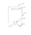
- FIG. 3 is a plan view showing an example of the shape of the glass substrate for cover glass.
- the glass substrate 1 for cover glass has an outer shape 1a, a notch 1b, an ear hole 1c, and a key operation hole 1d.
- Such drilling and outer peripheral shape processing may be machined by sandblasting or the like, or these drilling processing and outer peripheral shape processing may be collectively performed by etching.
- etching is advantageous for complex shape processing. Note that the etching method is the same as the etching method in the above-described cutting process. Moreover, you may use together machining and an etching process according to a process shape.
- the chemical strengthening treatment method for example, a low temperature type ion exchange method in which ion exchange is performed in a temperature range that does not exceed the glass transition temperature, for example, a temperature of 300 degrees Celsius or more and 400 degrees Celsius or less is preferable.
- the chemical strengthening treatment is a process in which a molten chemical strengthening salt is brought into contact with a glass substrate, whereby an alkali metal element having a relatively large atomic radius in the chemical strengthening salt and a relatively small atomic radius in the glass substrate.
- This is a treatment in which an alkali metal element is ion-exchanged, an alkali metal element having a large ion radius is permeated into the surface layer of the glass substrate, and compressive stress is generated on the surface of the glass substrate.
- alkali metal nitric acid such as potassium nitrate and sodium nitrate can be preferably used.
- a chemically strengthened glass substrate is improved in strength and excellent in impact resistance, and thus is suitable for a cover glass used for a portable device that requires impact and pressure and requires high strength.
- the manufacturing method of the cover glass for portable devices as the cover glass for electronic devices of the present invention includes a printing step of printing on the surface of the glass substrate for cover glass, and a step of forming a protective film on the glass substrate for cover glass; Before the printing step, a step of modifying the surface of the protective film corresponding to at least the region to be printed so that the printing is possible, and in the printing step, the modifying treatment In the printed area, printing is performed on the area to be printed.
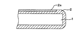
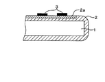
- FIG. 1A to 1C are schematic cross-sectional views for explaining a first embodiment of a method for manufacturing a cover glass for portable equipment as a cover glass for electronic equipment according to the present invention.
- the protective film 2 is formed in the whole surface of the glass substrate 1 for cover glasses.
- the glass substrate 1 for cover glass in this case is a glass substrate subjected to the above-described chemical strengthening treatment.
- the surface of the glass substrate 1 and the end surface of the protective film 2 are mounted on the jig of the printing machine and repeatedly removed from the jig. Is to prevent (or suppress) the generation of scratches on the glass substrate 1 due to contact with the glass substrate 1 several times.
- a material containing a general organic polymer compound as the material of the protective film 2.
- the material of the protective film 2 there are points to be considered when selecting the material of the protective film 2. That is, when a desired printing layer is formed on the glass substrate 1 having the protective film 2 formed on the entire surface, and the completed cover glass is incorporated into a display screen portion of a portable device, the surface side of the cover glass (the side opposite to the printing surface) ) Is exposed to the surface.
- the display screen is directly touched with a finger and operated, and thus, dirt such as fingerprints is likely to adhere to the display screen.
- the protective film 2 even if it is directly touched (pressed) with a finger, it prevents or suppresses dirt such as fingerprints from being adhered, or even if dirt such as fingerprints adheres is prevented. It is preferable to select a material having soiling properties. It is also important to have excellent transparency.
- a material that prevents or suppresses the generation of scratches on the glass substrate 1 in the printing process has antifouling properties, and is excellent in transparency, for example, a fluorine resin material (for example, perfluorocarbon)
- a material that lowers the surface energy such as a polyether compound or the like, or a silicon-based resin material (such as a silicone resin) is preferable.
- the protective film 2 can be applied and formed by a dip method, for example.
- the dipping method is performed by immersing the glass substrate 1 for cover glass in a coating solution containing, for example, the fluororesin or silicon resin as a main component in an appropriate solvent, and taking it out and drying it.
- the protective film 2 having a uniform thickness can be formed on the entire surface of the glass substrate 1 for cover glass.
- the coating thickness of the protective film 2 is not particularly limited, but is preferably in the range of 0.5 nm to 3000 nm, for example. If the film thickness is less than 0.5 nm, the protective film function in the printing process may not be sufficiently exhibited. On the other hand, when the film thickness exceeds 3000 nm, the transparency is lowered, so that the protective film request for the portable device is not met.
- FIG. 1B At least the surface of the protective film 2 corresponding to the region to be printed is subjected to a modification process so that printing is possible.
- What is indicated by reference numeral 2a in FIG. 1B is a modified layer formed on the surface layer of the protective film 2 by such modification treatment.
- the surface of the protective film 2 is modified to enable printing.
- the screen printing method is generally used as the cover glass printing method.
- a modification process that reduces the contact angle with water on the surface of the protective film 2.
- the modification treatment for reducing the contact angle with water on the surface of the protective film 2 include a method of exposing the surface of the protective film 2 to ultraviolet irradiation or oxygen plasma exposure.
- conditions such as irradiation energy and irradiation amount (irradiation time) in the case of performing ultraviolet irradiation, and conditions such as plasma energy and exposure time in the case of oxygen plasma exposure, preferable conditions can be selected as appropriate. Note that it is possible to adjust the thickness in the depth direction of the modified layer 2a formed on the surface layer of the protective film 2 by these ultraviolet irradiation conditions or oxygen plasma exposure conditions.
- the cover glass is usually incorporated with the printed layer side facing the inside of the portable device, the surface of the protective film on the surface to be incorporated in the portable device is modified. Further, in the present embodiment, it is necessary to modify the surface of the protective film 2 corresponding to at least the region to be printed so that printing is possible.
- the present invention is not limited to this. It is possible to set a region wider than the region where printing is actually performed (that is, including a region other than the printing region) and to modify the surface of the protective film 2 corresponding to the region for the convenience of the quality processing means. There is no problem.
- a printing process is performed. That is, a desired printing layer (ink layer) 3 is formed in a region to be printed out of the modified region.
- the modified layer 2a is subjected to a modification process that reduces the contact angle of the surface with water so that printing can be performed. Desired printing can be performed by screen printing or the like.
- the operation of loading and removing the glass substrate from the jig of the printing press is repeated according to the number of times of printing. In this embodiment, the jig of the printing press is used.
- the protective film 2 is formed on the end surface and the back surface (surface opposite to the printing surface) of the glass substrate 1 in contact with the glass, the glass is formed by the back surface and end surface of the glass substrate 1 coming into contact with the jig many times.
- substrate 1 can be prevented effectively (or suppressed).
- the cover glass thus completed is incorporated into a portable device.
- the method for manufacturing a cover glass for portable devices of the present embodiment even if a protective film is formed on the surface of the glass substrate for chemically strengthened cover glass, the protective film on the printed surface side It is possible to perform printing directly by modifying the surface, and the protective film can prevent (or suppress) the generation of scratches on the glass substrate during the printing process.
- a transparent conductive layer is formed on the main surface side of the glass substrate 1 that is incorporated toward the inside of the portable device (that is, the modified protective film surface side).
- a touch sensor module for detecting the operation of the user is used.
- the present invention also provides a method for manufacturing such a touch sensor module. That is, this invention is a manufacturing method of the touch sensor module for providing a glass substrate for cover glasses, and detecting a user's operation, Comprising: This manufacturing method forms a transparent conductive film with respect to the said glass substrate.
- the protective film is formed before the film forming process and enables the film formation on the glass substrate including a film forming process and having a protective film formed on the entire outer surface of the glass substrate.
- a method of manufacturing a touch sensor module comprising: a step of modifying or removing; and a film forming step of forming a film on the surface of the modified protective film or the glass substrate surface from which the protective film has been removed. It is.
- the present invention may further include a printing step that is performed before the film forming step, and that prints on a surface of the glass substrate for cover glass.
- the removing step is performed before the printing step instead of the film forming step, and the printing step performs printing on the modified protective film surface or the glass substrate surface from which the protective film has been removed,
- the film forming step includes forming a transparent conductive film on the modified protective film surface or the glass substrate surface from which the protective film is removed after the printing step. is there.
- the protective film 2 is formed on the end surface and the back surface of the glass substrate 1 (the surface opposite to the printing surface). It is possible to effectively prevent (or suppress) the generation of scratches on the glass substrate 1 due to the back surface and the end surface coming into contact with the jig of the transparent conductive layer film forming means (film forming apparatus or the like).
- the transparent conductive layer is formed with a predetermined thickness.
- the “predetermined thickness” of the transparent conductive layer is, for example, 100 nm or less when formed by a sputtering method, and includes a transparent resin serving as a binder when formed by a printing method. 1000 nm or less.
- a transparent conductive layer for example, an ITO (Indium Tin Oxide) film is formed using a sputtering method or the like, and laser patterning using a photolithography technique, a YAG (Yttrium Aluminum Garnet) fundamental wave, a CO 2 laser, or the like. It is formed by processing the transparent conductive layer into a desired pattern shape using a technique.
- the connection part metal wiring is formed by forming a metal conductive material on the surface of the printing region of the glass substrate by using a sputtering method or the like, and using a photolithography technique or the like to form the metal film. Is formed into a desired pattern shape.
- an insulating layer is formed between the surface of the modified protective film and the transparent conductive layer, and between the surface of the modified protective film and the connecting portion (metal wiring), if necessary. Is done.
- This insulating layer is preferably formed using an insulating material having transparency, for example, an inorganic material such as SiO 2 .
- the insulating layer is preferably formed to a thickness of about 50 to 1000 mm using, for example, a sputtering method.
- (Second Embodiment) 2nd Embodiment of the manufacturing method of the cover glass for portable devices as a cover glass for electronic devices which concerns on this invention includes the printing process which prints on the surface of the glass substrate for cover glasses, The said glass substrate for cover glasses Forming a protective film on the substrate, and removing the protective film corresponding to at least the region to be printed before the printing step, and in the printing step, the region from which the protective film has been removed Of these, printing is performed on the area to be printed.
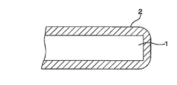
- FIGS. 2A to 2C are schematic cross-sectional views for explaining a second embodiment of a method for manufacturing a cover glass for a portable device as a cover glass for an electronic device according to the present invention.
- the protective film 2 is formed in the whole surface of the glass substrate 1 for cover glasses.
- the glass substrate 1 for cover glass in this case is a glass substrate that has been subjected to the above-described chemical strengthening treatment.
- steps from preparation of a glass substrate from a sheet-like glass material, external processing of the glass substrate, and chemical strengthening of the glass substrate Since this is the same as that of the first embodiment described above, redundant description is omitted here.
- the material, formation method, and the like of the protective film 2 are the same as those in the first embodiment.
- FIG. 2B shows a case where the entire protective film 2 on the printing surface side is removed as an example.
- the method for removing the protective film 2 varies depending on the material, but is not particularly limited in the present invention and is arbitrary.
- a desired printing layer (ink layer) 3 is formed in a region where printing is performed in the region where the protective film 2 is removed.
- desired printing can be performed directly on the surface of the glass substrate 1 by screen printing or the like.
- the operation of loading the glass substrate into the jig of the printing machine and removing it from the jig is repeated according to the number of times of printing.
- the protective film 2 is formed on at least the end surface and the back surface (surface opposite to the printing surface) of the glass substrate 1 that contacts the jig of the printing press, the back surface and the end surface of the glass substrate 1 are the jig. It is possible to effectively prevent (or suppress) the generation of scratches on the glass substrate 1 due to contact with the glass substrate 1 several times.
- the protective film on at least the printing area on the printing surface side is removed so that there is no protective film.
- the printing surface only comes into contact with, for example, a screen printing plate, and the jig of the printing machine. Since there is no direct contact with the surface, there is a very low possibility that scratches that affect the strength of the glass substrate on the printed surface side will occur.
- the cover glass is usually incorporated with the printed layer side facing the inside of the portable device, the protective film on the surface to be incorporated in the portable device is removed.
- the protective film on the surface to be incorporated in the portable device is removed.
- at least the protective film 2 corresponding to the region to be printed needs to be removed.
- the present invention is not limited to this.
- printing is actually performed. In some cases, it is necessary to remove the protective film 2 corresponding to an area wider than the area (that is, including an area other than the printing area).
- the cover glass thus completed is incorporated into a portable device.
- the method for manufacturing a cover glass for a portable device of the present embodiment even if a protective film is formed on the surface of the glass substrate for chemically strengthened cover glass, the protective film in the printing region is removed.
- printing can be performed directly, and the protective film formed on the glass substrate can prevent (or suppress) the occurrence of scratches on the glass substrate during the printing process.
- the transparent conductive layer is formed on the region side from which the protective film has been removed in addition to the printed layer to form a touch sensor module
- the end surface and the back surface of the glass substrate 1 (the above-mentioned Since the protective film 2 is formed on the surface opposite to the printing surface, the back surface and the end surface of the glass substrate 1 come into contact with the jig of the transparent conductive layer film forming means (film forming apparatus, etc.). Generation of scratches on the glass substrate 1 can be effectively prevented (or suppressed).
- Example 1 This implementation is performed through the following (1) glass substrate processing step, (2) shape processing step, (3) chemical strengthening step, (4) protective film forming step, (5) reforming treatment step, and (6) printing step.
- An example cover glass was made.
- a glass substrate for cover glass was produced by cutting out a predetermined size from a 0.5 mm thick plate glass made of an aluminosilicate gate glass produced by a downdraw method or a float method.
- a chemical containing SiO 2 : 58 to 75 wt%, Al 2 O 3 : 5 to 23 wt%, Li 2 O: 3 to 10 wt%, Na 2 O: 4 to 13 wt% Tempered glass was used.
- the protective film corresponding to the region to be printed on the printing surface side was irradiated with ultraviolet rays.
- Ultraviolet irradiation was performed using a high-pressure mercury lamp (200 W, 185 nm wavelength component 30%), and the irradiation time was 15 seconds.
- the contact angle with water on the surface of the protective film before the ultraviolet irradiation was 120 degrees
- the contact angle after the ultraviolet irradiation decreased to 10 degrees or less. Note that after a while after the ultraviolet irradiation, the contact angle was 20 degrees, and the numerical value slightly increased. Therefore, when ultraviolet irradiation is performed as the modification treatment, it is considered desirable to perform the next printing process before a long time has elapsed after irradiation.
- Printing process The printing process was implemented with respect to the glass substrate which performed the modification
- the modification process is performed to reduce the contact angle of the protective film surface with water so that printing can be performed by irradiating the surface of the protective film corresponding to the printing area on the printing surface side with the ultraviolet rays. Therefore, desired printing could be performed on the surface of the protective film (modified layer). Further, the print quality (according to the visual evaluation of the skilled worker) was a level at which there was no problem as a product. Thus, the cover glass of this example was completed.
- Example 2 A cover glass in the same manner as in Example 1 except that, in (5) the modification treatment step of Example 1, the protective film corresponding to the region to be printed on the printing surface side was subjected to atmospheric pressure plasma exposure treatment. Manufactured. The atmospheric pressure plasma exposure treatment was performed at RF output: 3.0 kW, N2 gas flow rate: 50 NL / min, CDA: 250 NmL / min, treatment time: 1 minute. The contact angle with water on the surface of the protective film before the oxygen plasma exposure was 130 degrees, but the contact angle after the oxygen plasma exposure (immediately after) decreased to 10 degrees or less.
- cover glass of this example obtained in this way, printing with good print quality could be performed on the protective film surface (modified layer).
- the protective film of the cover glass of this example was removed, and when the surface and end surface of the glass substrate were inspected in detail using an optical microscope, the occurrence of scratches on the glass substrate was detected. There wasn't. That is, also in the cover glass of the present embodiment, it is possible to effectively prevent generation of scratches on the glass substrate due to repeated contact with the jig in the printing process.
- Example 3 Instead of the (5) reforming process in Example 1, the protective film corresponding to the area to be printed on the printing surface side is removed, and in the subsequent (6) printing process, printing is performed on the area from which the protective film has been removed. A layer was formed. Except for this, a cover glass was produced in the same manner as in Example 1.
- cover glass of this example obtained in this way, it was possible to print with good print quality in the area where the protective film was removed. Moreover, when the remaining protective film of the cover glass of a present Example was removed and the surface and end surface of a glass substrate were inspected in detail using the optical microscope similarly to Example 1, generation
- Example 4 In the protective film formation (antifouling coating) step of Example 1, a coating liquid (liquid temperature: 25 ° C.) prepared by adjusting Shin-Etsu Chemical Co., Ltd. (trade name) KY100 series to an appropriate concentration with a solvent as a fluororesin. ) was applied to the entire surface of the glass substrate after the chemical strengthening by a dipping method, and dried with hot air at 100 ° C. to form a protective film having a coating thickness of 10 nm. A cover glass was produced in the same manner as in Example 1 except for this. In addition, the contact angle with respect to the water on the surface of the protective film before and after the modification of the protective film by the ultraviolet irradiation was the same as that in Example 1.
- cover glass of this example obtained in this way, printing with good print quality could be performed on the protective film surface (modified layer).
- the protective film of the cover glass of this example was removed, and when the surface and end surface of the glass substrate were inspected in detail using an optical microscope, the occurrence of scratches on the glass substrate was detected. There wasn't. That is, also in the cover glass of the present embodiment, it is possible to effectively prevent generation of scratches on the glass substrate due to repeated contact with the jig in the printing process.
- Example 1 The same printing process as in Example 1 was performed on the glass substrate that had been subjected to the chemical strengthening process in the same manner as in Example 1, without forming the protective film.
- cover glass of this comparative example thus obtained, printing with good print quality could be performed on the surface of the chemically strengthened glass substrate.
- the surface and end surface of the glass substrate were inspected in detail using an optical microscope, the occurrence of scratches on the glass substrate was detected, and in particular, there were many on the end surface and back surface of the glass substrate that were in direct contact with the jig of the printing press. A wound was found.
- the cover glass of this comparative example since the protective film is not formed before the printing process, it is possible to prevent the glass substrate from being damaged due to repeated contact with the jig in the printing process. Can not.
- Example 2 A cover glass was produced in the same manner as in Example 1 except that (5) the modification treatment step of Example 1 was omitted.
- the cover glass of this comparative example obtained in this way was not subjected to a modification treatment that would allow printing on the protective film in the printing area, so it could be printed temporarily, but it was required for the product. A certain level of print quality could not be obtained.
- the protective film of the cover glass of this comparative example was removed and the surface and end surface of the glass substrate were inspected in detail using the optical microscope, generation
Landscapes
- Engineering & Computer Science (AREA)
- Theoretical Computer Science (AREA)
- General Engineering & Computer Science (AREA)
- Chemical & Material Sciences (AREA)
- Chemical Kinetics & Catalysis (AREA)
- General Physics & Mathematics (AREA)
- Life Sciences & Earth Sciences (AREA)
- Physics & Mathematics (AREA)
- Human Computer Interaction (AREA)
- General Chemical & Material Sciences (AREA)
- Geochemistry & Mineralogy (AREA)
- Materials Engineering (AREA)
- Organic Chemistry (AREA)
- Surface Treatment Of Glass (AREA)
- Printing Methods (AREA)
- Devices For Indicating Variable Information By Combining Individual Elements (AREA)
Abstract
電子機器に用いられるカバーガラスの製造方法であって、カバーガラス用ガラス基板の表面に印刷を施す印刷工程を含み、カバーガラス用ガラス基板の全面に保護膜を形成する工程と、前記印刷工程の前に、少なくとも印刷を施す領域に相当する前記保護膜の表面を印刷が可能となるように改質処理する工程とを有する。前記印刷工程では、改質処理された領域のうち前記印刷を施す領域に印刷を施す。
Description
本発明は、携帯電話やPDA(Personal Digital Assistant)等の携帯機器の表示画面の保護に用いられる携帯機器用カバーガラスと、タッチセンサのセンサ基板に対するカバー部材であるタッチセンサ用カバーガラスとを含む電子機器用カバーガラスの製造方法、電子機器用カバーガラス、及び電子機器に用いられるカバーガラス用ガラス基板、並びにタッチセンサモジュールの製造方法に関するものである。
従来、携帯電話やPDA等の携帯機器(電子機器)の表示画面を保護するために、透明性に優れ且つ軽量なアクリル樹脂板が一般に用いられていた。近年、タッチパネル方式の携帯機器が主流を占めるようになり、このタッチパネル機能対応のため表示画面の強度向上が求められており、従来のアクリル樹脂材料に替わって、薄くても高い強度を有するガラス材料が多く使用されるようになってきている。さらに、ガラス材料は、従来のアクリル樹脂材料と比べると、機械的強度(耐加傷性、耐衝撃性)、表面平滑性、保護性(耐候性、防汚性)見栄え・高級感、価格など、いずれの点でも優位である。
このようなガラス材料からなるカバーガラスは、概ね次のようなプロセスで製造されている。
シート状に成形されたガラス素材を機械加工(カッティング)あるいはエッチング加工等で所定の大きさに小片化し、カバーガラス用ガラス基板を作製する。
次に、このガラス基板に対して機械加工あるいはエッチング加工により、必要な孔明け加工や外周形状加工などを行う。
シート状に成形されたガラス素材を機械加工(カッティング)あるいはエッチング加工等で所定の大きさに小片化し、カバーガラス用ガラス基板を作製する。
次に、このガラス基板に対して機械加工あるいはエッチング加工により、必要な孔明け加工や外周形状加工などを行う。
次に、形状加工を終えたガラス基板に化学強化処理を行う。この化学強化処理とは、ガラス中のナトリウムNa+をイオン半径の大きいカリウムK+と交換させ、ガラス表面に圧縮応力層を形成する処理法である。カバーガラスは、衝撃、押圧が加わるため高い強度が必要である。
次いで、以上の化学強化処理を行ったガラス基板の表面に所望の印刷を施す。
こうして出来上がったカバーガラスは、携帯機器に組み込まれる。
次いで、以上の化学強化処理を行ったガラス基板の表面に所望の印刷を施す。
こうして出来上がったカバーガラスは、携帯機器に組み込まれる。
上記のように、カバーガラス用ガラス基板は、その強度を向上させるため化学強化処理を行っている。ところで、カバーガラスの強度を阻害する要因の一つは傷である。カバーガラスの表面や端面に傷があるとそれが成長し、比較的弱い衝撃でもカバーガラスが破壊する要因となる。
上述のカバーガラスの製造プロセスでは、カバーガラス用ガラス基板に対して化学強化処理を行った後、印刷工程を行っている。カバーガラスの印刷方式は一般的にはスクリーン印刷である。通常、スクリーン印刷機に付属した位置合わせ治具に上記ガラス基板を1枚ずつ装填して、順次印刷層を塗り重ねていく。例えば最初に印刷層Aを印刷した後に、ガラス基板を治具から取り外し、熱硬化インキであれば60~100℃程度の温度で加熱し、UV硬化インキであれば指定積算エネルギーの紫外線(UV)を照射して印刷層Aを予備乾燥する。次に、印刷層Bのスクリーンが装着された印刷機に付属した位置合わせ治具に上記印刷層Aを印刷したガラス基板を装填して、印刷層Bの印刷を行い、再度ガラス基板を治具から取り外した後に印刷層Bを予備乾燥するといった作業を繰り返す。
従って、印刷工程において、このようなガラス基板の治具への装填、治具からの取り外しの作業を繰り返すことに伴って、ガラス基板の表面や端面が治具と何度も接触することによる傷が発生する恐れがある。例えば携帯電話のカバーガラスの例を挙げると、社名や製品名のロゴ、タッチパネル等のアイコン、各種センサー窓、画面周りの縁取り、裏面の押さえ印刷など、少なくとも2層、多いものでは例えば8層構成といった多色多層印刷を必要とする製品もあり、特に最近では印刷層の積層数が増える傾向にある。このように印刷回数が多くなるほど傷発生の可能性が高くなる。
特許文献1には、強化ガラス板にスクリーン印刷等の方法によって直接インキ像を形成するかわりに、強化ガラス板の一方の面に文字または模様の印刷を施したフィルムを貼付し、あるいは文字または模様の焼付け塗装を施し、他方の面にはフィルム状の飛散防止皮膜を貼付した携帯型表示装置用保護板が開示されている。この飛散防止皮膜は、強化ガラス板が破損した場合に破片が散らばるのを防止するためのものである。
また、特許文献2には、ガラス板の表面にフッ素系保護膜を施すことが記載されており、このフッ素系保護膜の成膜方法の一例としてディップ法が記載されている。
また、特許文献2には、ガラス板の表面にフッ素系保護膜を施すことが記載されており、このフッ素系保護膜の成膜方法の一例としてディップ法が記載されている。
上記特許文献1、特許文献2には、化学強化工程の後に実施する印刷工程で、化学強化されたガラス基板の表面や端面に傷が発生する恐れがあることは記載されておらず、これら特許文献に開示された先行技術では、上述の印刷工程でガラス基板に傷が発生することを防止することはできない。また、特許文献2に開示されているようにディップ法によってガラス板の表面にフッ素系保護膜を形成すると、スクリーン印刷等によって直接印刷層を形成すること自体が困難になってしまう。
本発明はこのような従来の課題を解決すべくなされたものであって、その目的は、化学強化されたカバーガラス用ガラス基板の表面に直接印刷を施すことが可能で、しかも印刷時のガラス基板の傷発生を防止することが可能な電子機器用カバーガラスの製造方法、及び上記ガラス基板の表面に透明導電膜の成膜を施すことが可能で、しかも成膜時のガラス基板の傷発生を防止することが可能なタッチセンサモジュールの製造方法を提供することである。
本発明者は、上記課題を解決すべく鋭意検討した結果、以下の構成を有する発明によれば上記課題を解決できることを見出した。
すなわち、本発明は以下の構成を有する。
(構成1)
電子機器に用いられるカバーガラスの製造方法であって、該製造方法は、カバーガラス用ガラス基板の表面に印刷を施す印刷工程を含み、前記カバーガラス用ガラス基板に保護膜を形成する工程と、前記印刷工程の前に、少なくとも前記印刷を施す領域に相当する前記保護膜の表面を前記印刷が可能となるように改質処理する工程とを有し、前記印刷工程では、前記改質処理された領域のうち前記印刷を施す領域に印刷を施すことを特徴とする電子機器用カバーガラスの製造方法である。
すなわち、本発明は以下の構成を有する。
(構成1)
電子機器に用いられるカバーガラスの製造方法であって、該製造方法は、カバーガラス用ガラス基板の表面に印刷を施す印刷工程を含み、前記カバーガラス用ガラス基板に保護膜を形成する工程と、前記印刷工程の前に、少なくとも前記印刷を施す領域に相当する前記保護膜の表面を前記印刷が可能となるように改質処理する工程とを有し、前記印刷工程では、前記改質処理された領域のうち前記印刷を施す領域に印刷を施すことを特徴とする電子機器用カバーガラスの製造方法である。
(構成2)
ガラス基板を備える電子機器用カバーガラスの製造方法であって、該製造方法は、前記ガラス基板の表面に印刷を施す印刷工程を含み、前記ガラス基板の外面全体に保護膜が形成された前記ガラス基板に対して、前記印刷工程の前に、少なくとも前記印刷を施す領域に相当する前記保護膜の表面を前記印刷が可能となるように改質処理する工程と、前記改質処理された領域のうち前記印刷を施す領域に印刷を施す前記印刷工程とを含むことを特徴とする電子機器用カバーガラスの製造方法である。
ガラス基板を備える電子機器用カバーガラスの製造方法であって、該製造方法は、前記ガラス基板の表面に印刷を施す印刷工程を含み、前記ガラス基板の外面全体に保護膜が形成された前記ガラス基板に対して、前記印刷工程の前に、少なくとも前記印刷を施す領域に相当する前記保護膜の表面を前記印刷が可能となるように改質処理する工程と、前記改質処理された領域のうち前記印刷を施す領域に印刷を施す前記印刷工程とを含むことを特徴とする電子機器用カバーガラスの製造方法である。
(構成3)
電子機器に用いられるカバーガラスの製造方法であって、該製造方法は、カバーガラス用ガラス基板の表面に印刷を施す印刷工程を含み、前記カバーガラス用ガラス基板に保護膜を形成する工程と、前記印刷工程の前に、少なくとも前記印刷を施す領域に相当する前記保護膜を除去する工程とを有し、前記印刷工程では、前記保護膜が除去された領域のうち前記印刷を施す領域に印刷を施すことを特徴とする電子機器用カバーガラスの製造方法である。
電子機器に用いられるカバーガラスの製造方法であって、該製造方法は、カバーガラス用ガラス基板の表面に印刷を施す印刷工程を含み、前記カバーガラス用ガラス基板に保護膜を形成する工程と、前記印刷工程の前に、少なくとも前記印刷を施す領域に相当する前記保護膜を除去する工程とを有し、前記印刷工程では、前記保護膜が除去された領域のうち前記印刷を施す領域に印刷を施すことを特徴とする電子機器用カバーガラスの製造方法である。
(構成4)
ガラス基板を備える電子機器用カバーガラスの製造方法であって、該製造方法は、前記ガラス基板の表面に印刷を施す印刷工程を含み、前記ガラス基板の外面全体に保護膜が形成された前記ガラス基板に対して、前記印刷工程の前に、少なくとも前記印刷を施す領域に相当する前記保護膜を除去する工程と、前記保護膜が除去された領域のうち前記印刷を施す領域に印刷を施す前記印刷工程とを含むことを特徴とする電子機器用カバーガラスの製造方法である。
ガラス基板を備える電子機器用カバーガラスの製造方法であって、該製造方法は、前記ガラス基板の表面に印刷を施す印刷工程を含み、前記ガラス基板の外面全体に保護膜が形成された前記ガラス基板に対して、前記印刷工程の前に、少なくとも前記印刷を施す領域に相当する前記保護膜を除去する工程と、前記保護膜が除去された領域のうち前記印刷を施す領域に印刷を施す前記印刷工程とを含むことを特徴とする電子機器用カバーガラスの製造方法である。
(構成5)
前記カバーガラス用ガラス基板は、化学強化されたアルミノシリケートガラスからなることを特徴とする構成1乃至4のいずれかに記載の電子機器用カバーガラスの製造方法である。
(構成6)
前記保護膜は、防汚性を有する材料からなることを特徴とする構成1乃至5のいずれかに記載の電子機器用カバーガラスの製造方法である。
前記カバーガラス用ガラス基板は、化学強化されたアルミノシリケートガラスからなることを特徴とする構成1乃至4のいずれかに記載の電子機器用カバーガラスの製造方法である。
(構成6)
前記保護膜は、防汚性を有する材料からなることを特徴とする構成1乃至5のいずれかに記載の電子機器用カバーガラスの製造方法である。
(構成7)
前記保護膜は、フッ素系樹脂材料又はシリコン系樹脂材料からなることを特徴とする構成6に記載の電子機器用カバーガラスの製造方法である。
(構成8)
前記保護膜をディップ法によって形成することを特徴とする構成1乃至7のいずれかに記載の電子機器用カバーガラスの製造方法である。
前記保護膜は、フッ素系樹脂材料又はシリコン系樹脂材料からなることを特徴とする構成6に記載の電子機器用カバーガラスの製造方法である。
(構成8)
前記保護膜をディップ法によって形成することを特徴とする構成1乃至7のいずれかに記載の電子機器用カバーガラスの製造方法である。
(構成9)
前記改質処理は、前記保護膜の表面における水に対する接触角を小さくする処理であることを特徴とする構成1、2、5乃至8のいずれかに記載の電子機器用カバーガラスの製造方法である。
(構成10)
前記改質処理は、前記保護膜の表面を紫外線照射または酸素プラズマ曝露する処理であることを特徴とする構成9に記載の電子機器用カバーガラスの製造方法である。
前記改質処理は、前記保護膜の表面における水に対する接触角を小さくする処理であることを特徴とする構成1、2、5乃至8のいずれかに記載の電子機器用カバーガラスの製造方法である。
(構成10)
前記改質処理は、前記保護膜の表面を紫外線照射または酸素プラズマ曝露する処理であることを特徴とする構成9に記載の電子機器用カバーガラスの製造方法である。
(構成11)
前記電子機器に組み込む側の面の前記保護膜の表面を改質処理することを特徴とする構成1、2、5乃至10のいずれかに記載の電子機器用カバーガラスの製造方法である。
(構成12)
前記電子機器に組み込む側の面の前記保護膜を除去することを特徴とする構成3乃至8のいずれかに記載の電子機器用カバーガラスの製造方法である。
前記電子機器に組み込む側の面の前記保護膜の表面を改質処理することを特徴とする構成1、2、5乃至10のいずれかに記載の電子機器用カバーガラスの製造方法である。
(構成12)
前記電子機器に組み込む側の面の前記保護膜を除去することを特徴とする構成3乃至8のいずれかに記載の電子機器用カバーガラスの製造方法である。
(構成13)
前記カバーガラス用ガラス基板の厚さは、0.3mm~1.5mmであることを特徴とする構成1乃至12のいずれかに記載の電子機器用カバーガラスの製造方法である。
(構成14)
電子機器に用いられるカバーガラス用のガラス基板であって、前記ガラス基板の表面に印刷層を形成する印刷工程において前記ガラス基板の表面の傷の発生を防止するため、前記ガラス基板の表面に保護膜を形成してなることを特徴とする電子機器に用いられるカバーガラス用ガラス基板である。
前記カバーガラス用ガラス基板の厚さは、0.3mm~1.5mmであることを特徴とする構成1乃至12のいずれかに記載の電子機器用カバーガラスの製造方法である。
(構成14)
電子機器に用いられるカバーガラス用のガラス基板であって、前記ガラス基板の表面に印刷層を形成する印刷工程において前記ガラス基板の表面の傷の発生を防止するため、前記ガラス基板の表面に保護膜を形成してなることを特徴とする電子機器に用いられるカバーガラス用ガラス基板である。
(構成15)
前記ガラス基板表面の前記印刷層が形成される領域は、印刷可能な領域とされていることを特徴とする構成14に記載の電子機器に用いられるカバーガラス用ガラス基板である。
(構成16)
構成14又は15に記載のカバーガラス用ガラス基板の表面に印刷層が形成された電子機器用カバーガラスである。
前記ガラス基板表面の前記印刷層が形成される領域は、印刷可能な領域とされていることを特徴とする構成14に記載の電子機器に用いられるカバーガラス用ガラス基板である。
(構成16)
構成14又は15に記載のカバーガラス用ガラス基板の表面に印刷層が形成された電子機器用カバーガラスである。
(構成17)
カバーガラス用ガラス基板を備え、利用者の操作を検出するためのタッチセンサモジュールの製造方法であって、該製造方法は、前記ガラス基板に対して透明導電膜を形成する成膜工程を含み、前記ガラス基板の外面全体に保護膜が形成された前記ガラス基板に対して、前記成膜工程の前に行われ、前記成膜が可能となるように、前記保護膜を改質又は除去する工程と、前記改質した前記保護膜表面、又は前記保護膜を除去したガラス基板表面に成膜を施す前記成膜工程とを含むことを特徴とするタッチセンサモジュールの製造方法である。
カバーガラス用ガラス基板を備え、利用者の操作を検出するためのタッチセンサモジュールの製造方法であって、該製造方法は、前記ガラス基板に対して透明導電膜を形成する成膜工程を含み、前記ガラス基板の外面全体に保護膜が形成された前記ガラス基板に対して、前記成膜工程の前に行われ、前記成膜が可能となるように、前記保護膜を改質又は除去する工程と、前記改質した前記保護膜表面、又は前記保護膜を除去したガラス基板表面に成膜を施す前記成膜工程とを含むことを特徴とするタッチセンサモジュールの製造方法である。
(構成18)
前記成膜工程の前に行われ、前記カバーガラス用ガラス基板の表面に印刷を施す印刷工程をさらに含み、前記保護膜を改質又は除去する工程は、前記成膜工程に代えて前記印刷工程の前に行われ、前記印刷工程は、前記改質した前記保護膜表面、又は前記保護膜を除去したガラス基板表面に印刷を施し、前記成膜工程は、前記印刷工程の後に、前記改質した前記保護膜表面、又は前記保護膜を除去したガラス基板表面に透明導電膜を形成することを特徴とする構成17に記載のタッチセンサモジュールの製造方法である。
前記成膜工程の前に行われ、前記カバーガラス用ガラス基板の表面に印刷を施す印刷工程をさらに含み、前記保護膜を改質又は除去する工程は、前記成膜工程に代えて前記印刷工程の前に行われ、前記印刷工程は、前記改質した前記保護膜表面、又は前記保護膜を除去したガラス基板表面に印刷を施し、前記成膜工程は、前記印刷工程の後に、前記改質した前記保護膜表面、又は前記保護膜を除去したガラス基板表面に透明導電膜を形成することを特徴とする構成17に記載のタッチセンサモジュールの製造方法である。
本発明によれば、化学強化されたカバーガラス用ガラス基板の表面に直接印刷を施すことが可能で、しかも印刷時のガラス基板の傷発生を防止することが可能な電子機器用カバーガラス及びその製造方法を提供することができる。
また、本発明によれば、上記ガラス基板の表面に透明導電膜の成膜を施すことが可能で、しかも成膜時のガラス基板の傷発生を防止することが可能なタッチセンサモジュールの製造方法を提供することができる。
また、本発明によれば、上記ガラス基板の表面に透明導電膜の成膜を施すことが可能で、しかも成膜時のガラス基板の傷発生を防止することが可能なタッチセンサモジュールの製造方法を提供することができる。
以下、本発明の実施の形態を詳述する。
(第1の実施の形態)
本発明に係るガラス材料からなる電子機器用カバーガラスとしての携帯機器用カバーガラスは、以下に説明するようなプロセスで製造される。
まず、シート状に成形されたガラス素材を機械加工等により所定の大きさにカッティング(小片化)し、カバーガラス用ガラス基板を作製する。
(第1の実施の形態)
本発明に係るガラス材料からなる電子機器用カバーガラスとしての携帯機器用カバーガラスは、以下に説明するようなプロセスで製造される。
まず、シート状に成形されたガラス素材を機械加工等により所定の大きさにカッティング(小片化)し、カバーガラス用ガラス基板を作製する。
ダウンドロー法やフロート法等で製造された厚さが例えば0.5mm程度のシート状ガラス素材(板ガラス)を多数枚(例えば数十枚程度)積層(ラミネート)し、ガラス用カッターを用いて所定の大きさの小片に切断する。勿論、シート状ガラス素材を1枚づつ加工してもよいが、積層状態のものを一度に切断加工すると、次の形状加工工程においても積層状態の小片を一度に形状加工できるので、生産上有利である。
小片の大きさは、製品のカバーガラスの大きさに外周形状加工に必要なマージンを加えた大きさを考慮して決定すればよい。
小片の大きさは、製品のカバーガラスの大きさに外周形状加工に必要なマージンを加えた大きさを考慮して決定すればよい。
なお、上記カバーガラス用ガラス基板の厚さは、最近の携帯機器の薄型化・軽量化のマーケットニーズに応える観点から例えば0.3mm~1.5mm程度の範囲であることが好ましく、さらに好ましくは0.5mm~0.7mm程度の範囲である。
本発明においては、カバーガラス用ガラス基板を構成するガラスは、アモルファスのアルミノシリケートガラスとすることが好ましい。このようなアルミノシリケートガラスからなるガラス基板は、化学強化後の強度が高く良好である。このようなアルミノシリケートガラスとしては、SiO2が58~75重量%、Al2O3が0~20重量%、Li2Oが0~10重量%、Na2Oが4~20重量%を主成分として含有するアルミノシリケートガラスを用いることができる。
なお、上述の機械加工以外の手段としては、エッチング法を適用することもできる。すなわち、上記シート状ガラス素材の表面にレジスト(感光性有機材料)を塗布し、所定の露光、現像を行って、カッティングラインのパターンを有するレジストパターン(カッティングライン上にはレジストが存在していないパターン)を形成する。そして、このようなレジストパターンを形成したガラス素材を溶解可能なエッチング液(例えばフッ酸を主成分とする酸性溶液など)を用いてウェットエッチングすることにより、所定の大きさの小片に切断する。残ったレジストパターンを剥離し、洗浄する。
次に、この所定の大きさの小片に加工されたカバーガラス用ガラス基板に対して機械加工あるいはエッチング加工により、必要な孔明け加工や外周形状加工などを行う。
図3はカバーガラス用ガラス基板の形状の一例を示す平面図である。図3に示す例では、カバーガラス用ガラス基板1は、外形抜き1a、切り欠き1b、耳孔1c、およびキー操作孔1dが形成されている。このような孔明け加工および外周形状加工をサンドブラスト等で機械加工してもよいし、あるいはエッチング加工により、これら孔明け加工および外周形状加工を一括処理することもできる。特に複雑な形状加工にはエッチング加工が有利である。なお、エッチング加工の方法は、上述の切断加工におけるエッチング加工法と同様である。また、加工形状に応じて機械加工とエッチング加工を併用してもよい。
次に、形状加工を終えたガラス基板に対して化学強化処理を行う。なお、ここまでガラス基板を積層状態のまま加工を行っていた場合には、化学強化の前に1枚づつ剥離(分離)しておく。
化学強化処理の方法としては、例えば、ガラス転移点の温度を超えない温度領域、例えば摂氏300度以上400度以下の温度で、イオン交換を行う低温型イオン交換法などが好ましい。化学強化処理とは、溶融させた化学強化塩とガラス基板とを接触させることにより、化学強化塩中の相対的に大きな原子半径のアルカリ金属元素と、ガラス基板中の相対的に小さな原子半径のアルカリ金属元素とをイオン交換し、ガラス基板の表層に該イオン半径の大きなアルカリ金属元素を浸透させ、ガラス基板の表面に圧縮応力を生じさせる処理のことである。化学強化塩としては、硝酸カリウムや硝酸ナトリウムなどのアルカリ金属硝酸を好ましく用いることができる。化学強化処理されたガラス基板は強度が向上し耐衝撃性に優れているので、衝撃、押圧が加わり高い強度が必要な携帯機器に用いられるカバーガラスには好適である。
次に、以上の化学強化処理を行ったガラス基板の表面に所望の印刷を施す。
本発明の電子機器用カバーガラスとしての携帯機器用カバーガラスの製造方法は、カバーガラス用ガラス基板の表面に印刷を施す印刷工程を含み、前記カバーガラス用ガラス基板に保護膜を形成する工程と、前記印刷工程の前に、少なくとも前記印刷を施す領域に相当する前記保護膜の表面を前記印刷が可能となるように改質処理する工程とを有し、前記印刷工程では、前記改質処理された領域のうち前記印刷を施す領域に印刷を施すことを特徴とするものである。
本発明の電子機器用カバーガラスとしての携帯機器用カバーガラスの製造方法は、カバーガラス用ガラス基板の表面に印刷を施す印刷工程を含み、前記カバーガラス用ガラス基板に保護膜を形成する工程と、前記印刷工程の前に、少なくとも前記印刷を施す領域に相当する前記保護膜の表面を前記印刷が可能となるように改質処理する工程とを有し、前記印刷工程では、前記改質処理された領域のうち前記印刷を施す領域に印刷を施すことを特徴とするものである。
以下、図1を参照して説明する。
図1A~図1Cは、本発明に係る電子機器用カバーガラスとしての携帯機器用カバーガラスの製造方法の第1の実施の形態を説明するための概略断面図である。
まず、図1Aに示すように、カバーガラス用ガラス基板1の全面に保護膜2を形成する。この場合のカバーガラス用ガラス基板1は、上述の化学強化処理を行ったガラス基板である。
図1A~図1Cは、本発明に係る電子機器用カバーガラスとしての携帯機器用カバーガラスの製造方法の第1の実施の形態を説明するための概略断面図である。
まず、図1Aに示すように、カバーガラス用ガラス基板1の全面に保護膜2を形成する。この場合のカバーガラス用ガラス基板1は、上述の化学強化処理を行ったガラス基板である。
上記保護膜2は、印刷工程において、このようなガラス基板1を印刷機の治具へ装填し、また治具から取り外すといった作業を繰り返すことに伴って、ガラス基板1の表面や端面が治具と何度も接触することによるガラス基板1の傷の発生を防止(ないしは抑制)するためのものである。
従って、上記保護膜2の材質としては、一般の有機ポリマー化合物を含有する材料を用いることが好適である。但し、上記保護膜2の材質を選択するに当たって考慮すべき点がある。すなわち、上記保護膜2を全面に形成したガラス基板1に所望の印刷層を形成し、出来上がったカバーガラスを携帯機器の表示画面部に組み込むと、カバーガラスの表面側(印刷面とは反対側)の保護膜が表に露出することになる。利用者がタッチパネル方式の携帯機器を使用する場合、その表示画面を指で直接触れて操作するため、表示画面に指紋等の汚れが付着しやすい。従って、表示画面に指紋等の汚れが付着するのを防止ないしは抑制し、あるいは指紋等の汚れが付着しても容易に拭き取れるようにすることが望ましい。そのためには、上記保護膜2の材質として、指で直接触れても(押しても)指紋等の汚れが付着するのを防止ないしは抑制し、あるいは指紋等の汚れが付着しても拭き取り易くする防汚性を有する材料を選択することが好適である。また、透明性に優れていることも重要である。
本発明においては、印刷工程におけるガラス基板1の傷発生を防止ないしは抑制し、且つ防汚性を有し、さらには透明性にも優れている材料としては、たとえばフッ素系樹脂材料(例えばパーフルオロポリエーテル化合物など)又はシリコン系樹脂材料(例えばシリコーン樹脂など)などの表面エネルギーを低下させる材料が好ましく挙げられる。
上記保護膜2は例えばディップ法によって塗布形成することができる。ディップ法は、適当な溶媒中に例えば上記フッ素系樹脂又はシリコン系樹脂を主成分として含有する塗布液中に上記カバーガラス用ガラス基板1を浸漬させ、これを取り出して乾燥することによって行われる。このディップ法によれば、上記カバーガラス用ガラス基板1の全面に均一な膜厚の保護膜2を形成することができる。
上記保護膜2の塗布膜厚は、特に制約されないが、例えば0.5nm~3000nmの範囲であることが好ましい。膜厚が0.5nm未満であると、印刷工程での保護膜機能が十分に発揮されない恐れがある。一方、膜厚が3000nmを超えると、透明性が低下するので携帯機器の保護膜要請に沿わなくなる。
次に、図1Bに示すように、少なくとも印刷を施す領域に相当する保護膜2の表面を印刷が可能となるように改質処理する。図1B中の符号2aで示すものはこのような改質処理により保護膜2の表層に形成された改質層である。
ガラス基板1上に保護膜2として例えば上記のフッ素系樹脂膜又はシリコン系樹脂膜を形成した場合、その保護膜2にスクリーン印刷等によって印刷層を形成することは困難である。本発明では、保護膜2の表面を改質処理して印刷が可能となるようにしている。
ガラス基板1上に保護膜2として例えば上記のフッ素系樹脂膜又はシリコン系樹脂膜を形成した場合、その保護膜2にスクリーン印刷等によって印刷層を形成することは困難である。本発明では、保護膜2の表面を改質処理して印刷が可能となるようにしている。
前述したように、カバーガラスの印刷方式としてはスクリーン印刷法が一般的である。上記保護膜2の表面にスクリーン印刷を可能とするためには、上記保護膜2の表面における水に対する接触角を小さくするような改質処理を施すことが好適である。このような保護膜2の表面における水に対する接触角を小さくするような改質処理としては、たとえば上記保護膜2の表面を紫外線照射または酸素プラズマ曝露する方法が挙げられる。紫外線照射を行う場合の照射エネルギー、照射量(照射時間)などの条件、また酸素プラズマ曝露する場合のプラズマエネルギー、曝露時間などの条件に関しては、好ましい条件を適宜選択して実施することができる。
なお、これら紫外線照射条件または酸素プラズマ曝露条件によって、保護膜2の表層に形成される改質層2aの深さ方向における厚さを調整することは可能である。
なお、これら紫外線照射条件または酸素プラズマ曝露条件によって、保護膜2の表層に形成される改質層2aの深さ方向における厚さを調整することは可能である。
なお、通常、カバーガラスの印刷層側を携帯機器の内側に向けて組み込まれるため、携帯機器に組み込む側の面の保護膜の表面を改質処理する。
また、本実施の形態においては、少なくとも印刷を施す領域に相当する保護膜2の表面を印刷が可能となるように改質処理する必要があるが、これには限定されず、たとえば適用する改質処理手段の都合等により、実際に印刷を施す領域よりも広い領域(つまり印刷領域以外の領域を含む)を設定して、その領域に相当する保護膜2の表面を改質処理することは差し支えない。
また、本実施の形態においては、少なくとも印刷を施す領域に相当する保護膜2の表面を印刷が可能となるように改質処理する必要があるが、これには限定されず、たとえば適用する改質処理手段の都合等により、実際に印刷を施す領域よりも広い領域(つまり印刷領域以外の領域を含む)を設定して、その領域に相当する保護膜2の表面を改質処理することは差し支えない。
次いで、図1Cに示すように、印刷工程を実施する。すなわち、上記改質処理された領域のうち印刷を施す領域に所望の印刷層(インキ層)3を形成する。上述したように、上記改質層2aには、たとえば印刷が可能となるように表面の水に対する接触角を小さくするような改質処理が施されているため、上記改質層2aの表面にスクリーン印刷等によって所望の印刷を施すことができる。また、この印刷工程においては、ガラス基板を印刷機の治具へ装填し、また治具から取り外すといった作業を印刷回数に応じて繰り返すことになるが、本実施の形態では、印刷機の治具と接触するガラス基板1の端面及び裏面(印刷面と反対側の面)には保護膜2が形成されているため、ガラス基板1の裏面や端面が治具と何度も接触することによるガラス基板1の傷の発生を有効に防止(ないしは抑制)することができる。
こうして出来上がったカバーガラスは、携帯機器に組み込まれる。
以上説明したように、本実施の形態の携帯機器用カバーガラスの製造方法によれば、化学強化されたカバーガラス用ガラス基板の表面に保護膜を形成しても、その印刷面側の保護膜表面を改質処理することで直接印刷を施すことが可能であり、しかもその保護膜によって印刷工程時のガラス基板の傷発生を防止(ないしは抑制)することができる。
以上説明したように、本実施の形態の携帯機器用カバーガラスの製造方法によれば、化学強化されたカバーガラス用ガラス基板の表面に保護膜を形成しても、その印刷面側の保護膜表面を改質処理することで直接印刷を施すことが可能であり、しかもその保護膜によって印刷工程時のガラス基板の傷発生を防止(ないしは抑制)することができる。
また、携帯機器の内側に向けて組み込まれるガラス基板1の主表面側(つまり上記改質処理された保護膜表面側)に、上記印刷層以外に、例えば透明導電層を形成して、携帯機器の利用者の操作を検出するためのタッチセンサモジュールとする場合がある。本発明は、このようなタッチセンサモジュールの製造方法についても提供するものである。
すなわち、本発明は、カバーガラス用ガラス基板を備え、利用者の操作を検出するためのタッチセンサモジュールの製造方法であって、該製造方法は、前記ガラス基板に対して透明導電膜を形成する成膜工程を含み、前記ガラス基板の外面全体に保護膜が形成された前記ガラス基板に対して、前記成膜工程の前に行われ、前記成膜が可能となるように、前記保護膜を改質又は除去する工程と、前記改質した前記保護膜表面、又は前記保護膜を除去したガラス基板表面に成膜を施す前記成膜工程とを含むことを特徴とするタッチセンサモジュールの製造方法である。
すなわち、本発明は、カバーガラス用ガラス基板を備え、利用者の操作を検出するためのタッチセンサモジュールの製造方法であって、該製造方法は、前記ガラス基板に対して透明導電膜を形成する成膜工程を含み、前記ガラス基板の外面全体に保護膜が形成された前記ガラス基板に対して、前記成膜工程の前に行われ、前記成膜が可能となるように、前記保護膜を改質又は除去する工程と、前記改質した前記保護膜表面、又は前記保護膜を除去したガラス基板表面に成膜を施す前記成膜工程とを含むことを特徴とするタッチセンサモジュールの製造方法である。
また、本発明は、上記タッチセンサモジュールの製造方法において、前記成膜工程の前に行われ、前記カバーガラス用ガラス基板の表面に印刷を施す印刷工程をさらに含み、前記保護膜を改質又は除去する工程は、前記成膜工程に代えて前記印刷工程の前に行われ、前記印刷工程は、前記改質した前記保護膜表面、又は前記保護膜を除去したガラス基板表面に印刷を施し、前記成膜工程は、前記印刷工程の後に、前記改質した前記保護膜表面、又は前記保護膜を除去したガラス基板表面に透明導電膜を形成することを特徴とするタッチセンサモジュールの製造方法である。
このような透明導電層を形成する場合においても、本発明では、ガラス基板1の端面及び裏面(上記印刷面と反対側の面)には保護膜2が形成されているため、ガラス基板1の裏面や端面が上記透明導電層の成膜手段(成膜装置等)の治具と接触することによるガラス基板1の傷の発生を有効に防止(ないしは抑制)することができる。
上記透明導電層は、所定の厚さをもって形成される。この透明導電層の「所定の厚さ」とは、スパッタリング法により成膜される場合には、例えば100nm以下であり、印刷法により成膜される場合には、バインダーとなる透明樹脂を含めて1000nm以下である。
具体的には、スパッタリング法等を用いて透明導電層、例えばITO(Indium Tin Oxide)膜を成膜し、フォトリソグラフィ技術、またはYAG(Yttrium Aluminum Garnet)の基本波やCO2レーザ等によるレーザパターニング技術を用いて透明導電層を所望のパターン形状に加工することにより形成される。また、接続部(金属配線)は、ガラス基板の印刷領域の表面にスパッタリング法等を用いて金属製の導電物質を成膜することにより金属膜を形成し、フォトリソグラフィ技術等を用いて金属膜を所望のパターン形状に加工することにより形成される。
また、上記改質処理された保護膜表面と透明導電層との間、上記改質処理された保護膜表面と接続部(金属配線)との間には、それぞれ必要に応じて絶縁層が形成される。この絶縁層は、透明性を有する絶縁性物質、例えば、SiO2等の無機材料を用いて形成されることが好ましい。また、絶縁層は、例えばスパッタリング法等を用いて、厚さ50~1000Å程度に形成されることが好ましい。
(第2の実施の形態)
本発明に係る電子機器用カバーガラスとしての携帯機器用カバーガラスの製造方法の第2の実施の形態は、カバーガラス用ガラス基板の表面に印刷を施す印刷工程を含み、前記カバーガラス用ガラス基板に保護膜を形成する工程と、前記印刷工程の前に、少なくとも前記印刷を施す領域に相当する前記保護膜を除去する工程とを有し、前記印刷工程では、前記保護膜が除去された領域のうち前記印刷を施す領域に印刷を施すことを特徴とするものである。
本発明に係る電子機器用カバーガラスとしての携帯機器用カバーガラスの製造方法の第2の実施の形態は、カバーガラス用ガラス基板の表面に印刷を施す印刷工程を含み、前記カバーガラス用ガラス基板に保護膜を形成する工程と、前記印刷工程の前に、少なくとも前記印刷を施す領域に相当する前記保護膜を除去する工程とを有し、前記印刷工程では、前記保護膜が除去された領域のうち前記印刷を施す領域に印刷を施すことを特徴とするものである。
以下、図2A~図2Cを参照して説明する。
図2A~図2Cは、本発明に係る電子機器用カバーガラスとしての携帯機器用カバーガラスの製造方法の第2の実施の形態を説明するための概略断面図である。
まず、図2Aに示すように、カバーガラス用ガラス基板1の全面に保護膜2を形成する。この場合のカバーガラス用ガラス基板1は、前述の化学強化処理を行ったガラス基板であるが、シート状ガラス素材からのガラス基板の作製、ガラス基板の外形加工、ガラス基板の化学強化までの工程は、上述の第1の実施の形態と同様であるので、ここでは重複説明は省略する。
上記保護膜2の材質、形成方法などについては上述の第1の実施の形態と同様である。
図2A~図2Cは、本発明に係る電子機器用カバーガラスとしての携帯機器用カバーガラスの製造方法の第2の実施の形態を説明するための概略断面図である。
まず、図2Aに示すように、カバーガラス用ガラス基板1の全面に保護膜2を形成する。この場合のカバーガラス用ガラス基板1は、前述の化学強化処理を行ったガラス基板であるが、シート状ガラス素材からのガラス基板の作製、ガラス基板の外形加工、ガラス基板の化学強化までの工程は、上述の第1の実施の形態と同様であるので、ここでは重複説明は省略する。
上記保護膜2の材質、形成方法などについては上述の第1の実施の形態と同様である。
次に、図2Bに示すように、本実施の形態では、印刷面側の少なくとも印刷を施す領域に相当する保護膜2を除去する。なお図2Bでは、一例として印刷面側の保護膜2の全部を除去した場合を示している。
保護膜2の除去方法はその材質によっても異なるが、本発明においては特に制約はなく任意である。
保護膜2の除去方法はその材質によっても異なるが、本発明においては特に制約はなく任意である。
次いで、図2Cに示すように、上記保護膜2が除去された領域のうち印刷を施す領域に所望の印刷層(インキ層)3を形成する。印刷を施す領域に相当する保護膜2を除去して、ガラス基板1の表面が露出することにより、ガラス基板1の表面に直接、スクリーン印刷等によって所望の印刷を施すことができる。また、前にも説明したように、この印刷工程においては、ガラス基板を印刷機の治具へ装填し、また治具から取り外すといった作業を印刷回数に応じて繰り返すことになるが、本実施の形態では、少なくとも印刷機の治具と接触するガラス基板1の端面及び裏面(印刷面と反対側の面)には保護膜2が形成されているため、ガラス基板1の裏面や端面が治具と何度も接触することによるガラス基板1の傷の発生を有効に防止(ないしは抑制)することができる。
なお、本実施の形態においては、印刷面側の少なくとも印刷領域の保護膜が除去されて保護膜がない状態となるが、印刷面は例えばスクリーン印刷版と接触するだけで、印刷機の治具とは直接接触しないため、印刷面側においてガラス基板の強度に影響を及ぼすような傷が発生する可能性は極めて低い。
また、通常、カバーガラスの印刷層側を携帯機器の内側に向けて組み込まれるため、携帯機器に組み込む側の面の保護膜を除去する。
また、本実施の形態においては、少なくとも印刷を施す領域に相当する保護膜2を除去する必要があるが、これには限定されず、たとえば適用する保護膜除去手段によっては、実際に印刷を施す領域よりも広い領域(つまり印刷領域以外の領域を含む)に相当する保護膜2を除去する必要がある場合もある。
また、本実施の形態においては、少なくとも印刷を施す領域に相当する保護膜2を除去する必要があるが、これには限定されず、たとえば適用する保護膜除去手段によっては、実際に印刷を施す領域よりも広い領域(つまり印刷領域以外の領域を含む)に相当する保護膜2を除去する必要がある場合もある。
こうして出来上がったカバーガラスは、携帯機器に組み込まれる。
以上説明したように、本実施の形態の携帯機器用カバーガラスの製造方法によれば、化学強化されたカバーガラス用ガラス基板の表面に保護膜を形成しても印刷領域の保護膜を除去することで直接印刷を施すことが可能であり、しかもガラス基板に形成されている保護膜によって印刷工程時のガラス基板の傷発生を防止(ないしは抑制)することができる。
以上説明したように、本実施の形態の携帯機器用カバーガラスの製造方法によれば、化学強化されたカバーガラス用ガラス基板の表面に保護膜を形成しても印刷領域の保護膜を除去することで直接印刷を施すことが可能であり、しかもガラス基板に形成されている保護膜によって印刷工程時のガラス基板の傷発生を防止(ないしは抑制)することができる。
また、本実施の形態においても、上記保護膜が除去された領域側に、上記印刷層以外に、上記透明導電層を形成してタッチセンサモジュールとする場合、ガラス基板1の端面及び裏面(上記印刷面と反対側の面)には保護膜2が形成されているため、ガラス基板1の裏面や端面が上記透明導電層の成膜手段(成膜装置等)の治具と接触することによるガラス基板1の傷の発生を有効に防止(ないしは抑制)することができる。
以下に具体的実施例を挙げて、本発明をさらに具体的に説明する。ここでは、電子機器用カバーガラスとしての携帯機器用カバーガラスについて説明する。なお、本発明は以下の携帯機器用カバーガラスの実施例に限定されるものではない。
(実施例1)
以下の(1)ガラス基板加工工程、(2)形状加工工程、(3)化学強化工程、(4)保護膜形成工程、(5)改質処理工程、(6)印刷工程、を経て本実施例のカバーガラスを製造した。
(実施例1)
以下の(1)ガラス基板加工工程、(2)形状加工工程、(3)化学強化工程、(4)保護膜形成工程、(5)改質処理工程、(6)印刷工程、を経て本実施例のカバーガラスを製造した。
(1)ガラス基板加工工程
まず、ダウンドロー法やフロート法で製造されたアルミノシリゲートガラスからなる厚さ0.5mmの板ガラスから所定の大きさに切り出してカバーガラス用ガラス基板を作製した。このアルミノシリケートガラスとしては、SiO2:58~75重量%、Al2O3:5~23重量%、Li2O:3~10重量%、Na2O:4~13重量%を含有する化学強化用ガラスを使用した。
まず、ダウンドロー法やフロート法で製造されたアルミノシリゲートガラスからなる厚さ0.5mmの板ガラスから所定の大きさに切り出してカバーガラス用ガラス基板を作製した。このアルミノシリケートガラスとしては、SiO2:58~75重量%、Al2O3:5~23重量%、Li2O:3~10重量%、Na2O:4~13重量%を含有する化学強化用ガラスを使用した。
(2)形状加工工程
次に、砥石等を用いて上記ガラス基板に孔を空けると共に、例えば前述の図3に示すような外周端面の形状加工を施した。
次に、砥石等を用いて上記ガラス基板に孔を空けると共に、例えば前述の図3に示すような外周端面の形状加工を施した。
(3)化学強化工程
次に、上記形状加工を終えたガラス基板に化学強化を施した。化学強化は硝酸カリウムと硝酸ナトリウムの混合した化学強化液を用意し、この化学強化溶液を380℃に加熱し、上記形状加工後の洗浄・乾燥済みのガラス基板を約4時間浸漬して化学強化処理を行なった。化学強化を終えたガラス基板を硫酸、中性洗剤、純水、純水、IPA、IPA(蒸気乾燥)の各洗浄槽に順次浸漬して、超音波洗浄し、乾燥した。
次に、上記形状加工を終えたガラス基板に化学強化を施した。化学強化は硝酸カリウムと硝酸ナトリウムの混合した化学強化液を用意し、この化学強化溶液を380℃に加熱し、上記形状加工後の洗浄・乾燥済みのガラス基板を約4時間浸漬して化学強化処理を行なった。化学強化を終えたガラス基板を硫酸、中性洗剤、純水、純水、IPA、IPA(蒸気乾燥)の各洗浄槽に順次浸漬して、超音波洗浄し、乾燥した。
(4)保護膜形成(防汚コート)工程
フッ素系樹脂(スリーエム社製 EGC-1720)を溶剤で適当な濃度に調整した塗布液(液温25℃)を用いてディップ法により、上記化学強化を終えたガラス基板の全面に上記フッ素系樹脂からなる保護膜を塗布し、100℃で熱風乾燥した。保護膜の塗布膜厚は10nmとした。
フッ素系樹脂(スリーエム社製 EGC-1720)を溶剤で適当な濃度に調整した塗布液(液温25℃)を用いてディップ法により、上記化学強化を終えたガラス基板の全面に上記フッ素系樹脂からなる保護膜を塗布し、100℃で熱風乾燥した。保護膜の塗布膜厚は10nmとした。
(5)改質処理工程
次に、印刷面側の印刷を施す領域に相当する上記保護膜に対して紫外線照射を行った。紫外線照射は、高圧水銀ランプ(200W、185nm波長成分30%)を用いて行い、照射時間は15秒とした。
上記紫外線照射前の保護膜表面における水に対する接触角は120度であったが、上記紫外線照射後(直後)の接触角は10度以下に下がった。なお、上記紫外線照射後しばらく経過すると、上記接触角は20度となり若干数値が大きくなった。従って、改質処理として紫外線照射を行った場合、照射後あまり時間が経過しないうちに、次の印刷工程を行うことが望ましいと考えられる。
次に、印刷面側の印刷を施す領域に相当する上記保護膜に対して紫外線照射を行った。紫外線照射は、高圧水銀ランプ(200W、185nm波長成分30%)を用いて行い、照射時間は15秒とした。
上記紫外線照射前の保護膜表面における水に対する接触角は120度であったが、上記紫外線照射後(直後)の接触角は10度以下に下がった。なお、上記紫外線照射後しばらく経過すると、上記接触角は20度となり若干数値が大きくなった。従って、改質処理として紫外線照射を行った場合、照射後あまり時間が経過しないうちに、次の印刷工程を行うことが望ましいと考えられる。
(6)印刷工程
上記保護膜の改質処理を行ったガラス基板に対して印刷工程を実施した。
すなわち、上記保護膜が改質処理された領域のうち印刷を施す領域に、スクリーン印刷によって所定の印刷層(インキ層)を形成した。本実施例では、全部で8層の印刷層を形成した。なお、熱硬化インキを使用し、各印刷層の印刷後に60~100℃程度の温度で熱風乾燥した。また、各印刷層の印刷の度に保護膜付きガラス基板を印刷機の治具へ装填し、また治具から取り外すといった作業を印刷回数(8回)だけ繰り返した。
上記保護膜の改質処理を行ったガラス基板に対して印刷工程を実施した。
すなわち、上記保護膜が改質処理された領域のうち印刷を施す領域に、スクリーン印刷によって所定の印刷層(インキ層)を形成した。本実施例では、全部で8層の印刷層を形成した。なお、熱硬化インキを使用し、各印刷層の印刷後に60~100℃程度の温度で熱風乾燥した。また、各印刷層の印刷の度に保護膜付きガラス基板を印刷機の治具へ装填し、また治具から取り外すといった作業を印刷回数(8回)だけ繰り返した。
本実施例では、上述したように、印刷面側の印刷領域に相当する保護膜表面に上記紫外線照射を行ない、印刷が可能となるように保護膜表面の水に対する接触角を小さくする改質処理が施されているため、保護膜表面(改質層)に所望の印刷を施すことができた。また、印刷品質(熟練者の目視評価による)は、製品としてまったく問題のないレベルであった。
こうして本実施例のカバーガラスを完成した。
こうして本実施例のカバーガラスを完成した。
また、この完成したカバーガラスの保護膜を除去し、光学顕微鏡を用いて、ガラス基板の表面及び端面を詳細に検査したところ、ガラス基板に傷の発生は検出されなかった。つまり、印刷機の治具と接触するガラス基板の端面及び裏面(印刷面と反対側の面)には保護膜が形成されているため、治具と何度も接触することによるガラス基板の傷の発生を有効に防止することができる。
(実施例2)
実施例1の(5)改質処理工程において、印刷面側の印刷を施す領域に相当する保護膜に対して常圧プラズマ曝露処理を行ったこと以外は、実施例1と同様にしてカバーガラスを製造した。なお常圧プラズマ曝露処理は、RF出力:3.0kw、N2ガス流量:50NL/min、CDA:250NmL/min、処理時間:1分で行った。
上記酸素プラズマ曝露前の保護膜表面における水に対する接触角は130度であったが、上記酸素プラズマ曝露後(直後)の接触角は10度以下に下がった。
実施例1の(5)改質処理工程において、印刷面側の印刷を施す領域に相当する保護膜に対して常圧プラズマ曝露処理を行ったこと以外は、実施例1と同様にしてカバーガラスを製造した。なお常圧プラズマ曝露処理は、RF出力:3.0kw、N2ガス流量:50NL/min、CDA:250NmL/min、処理時間:1分で行った。
上記酸素プラズマ曝露前の保護膜表面における水に対する接触角は130度であったが、上記酸素プラズマ曝露後(直後)の接触角は10度以下に下がった。
こうして得られた本実施例のカバーガラスにおいても、保護膜表面(改質層)に、印刷品質の良好な印刷を施すことができた。また、実施例1と同様に、本実施例のカバーガラスの保護膜を除去し、光学顕微鏡を用いて、ガラス基板の表面及び端面を詳細に検査したところ、ガラス基板に傷の発生は検出されなかった。つまり、本実施例のカバーガラスにおいても、印刷工程での治具と何度も接触することによるガラス基板の傷の発生を有効に防止することができる。
(実施例3)
実施例1の(5)改質処理工程の代わりに、印刷面側の印刷を施す領域に相当する保護膜を除去し、その後の(6)印刷工程では、その保護膜を除去した領域に印刷層を形成した。これ以外は、実施例1と同様にしてカバーガラスを製造した。
実施例1の(5)改質処理工程の代わりに、印刷面側の印刷を施す領域に相当する保護膜を除去し、その後の(6)印刷工程では、その保護膜を除去した領域に印刷層を形成した。これ以外は、実施例1と同様にしてカバーガラスを製造した。
こうして得られた本実施例のカバーガラスにおいても、保護膜を除去した領域に、印刷品質の良好な印刷を施すことができた。また、本実施例のカバーガラスの残りの保護膜を除去し、実施例1と同様に、光学顕微鏡を用いて、ガラス基板の表面及び端面を詳細に検査したところ、ガラス基板に傷の発生は検出されなかった。つまり、本実施例のカバーガラスにおいても、印刷工程での治具と何度も接触することによるガラス基板の傷の発生を有効に防止することができる。
(実施例4)
実施例1の(4)保護膜形成(防汚コート)工程において、フッ素系樹脂として、信越化学工業社製(商品名)KY100シリーズを溶剤で適当な濃度に調整した塗布液(液温25℃)を用いてディップ法により、上記化学強化を終えたガラス基板の全面に上記フッ素系樹脂からなる保護膜を塗布し、100℃で熱風乾燥し、塗布膜厚10nmの保護膜を形成した。このこと以外は、実施例1と同様にしてカバーガラスを製造した。
なお、前記紫外線照射による上記保護膜の改質処理前後の保護膜表面における水に対する接触角はそれぞれ実施例1と同等であった。
実施例1の(4)保護膜形成(防汚コート)工程において、フッ素系樹脂として、信越化学工業社製(商品名)KY100シリーズを溶剤で適当な濃度に調整した塗布液(液温25℃)を用いてディップ法により、上記化学強化を終えたガラス基板の全面に上記フッ素系樹脂からなる保護膜を塗布し、100℃で熱風乾燥し、塗布膜厚10nmの保護膜を形成した。このこと以外は、実施例1と同様にしてカバーガラスを製造した。
なお、前記紫外線照射による上記保護膜の改質処理前後の保護膜表面における水に対する接触角はそれぞれ実施例1と同等であった。
こうして得られた本実施例のカバーガラスにおいても、保護膜表面(改質層)に、印刷品質の良好な印刷を施すことができた。また、実施例1と同様に、本実施例のカバーガラスの保護膜を除去し、光学顕微鏡を用いて、ガラス基板の表面及び端面を詳細に検査したところ、ガラス基板に傷の発生は検出されなかった。つまり、本実施例のカバーガラスにおいても、印刷工程での治具と何度も接触することによるガラス基板の傷の発生を有効に防止することができる。
(比較例1)
実施例1と同様に化学強化工程まで行ったガラス基板に対して、上記保護膜形成を行わずに、実施例1と同様の印刷工程を行った。
こうして得られた本比較例のカバーガラスにおいては、化学強化したガラス基板の表面に、印刷品質の良好な印刷を施すことができた。しかし、光学顕微鏡を用いて、ガラス基板の表面及び端面を詳細に検査したところ、ガラス基板に傷の発生が検出され、特に印刷機の治具と直接接触するガラス基板の端面及び裏面には多数の傷が発見された。つまり、本比較例のカバーガラスにおいては、印刷工程の前に保護膜が形成されていないため、印刷工程での治具と何度も接触することによるガラス基板の傷の発生を防止することができない。
実施例1と同様に化学強化工程まで行ったガラス基板に対して、上記保護膜形成を行わずに、実施例1と同様の印刷工程を行った。
こうして得られた本比較例のカバーガラスにおいては、化学強化したガラス基板の表面に、印刷品質の良好な印刷を施すことができた。しかし、光学顕微鏡を用いて、ガラス基板の表面及び端面を詳細に検査したところ、ガラス基板に傷の発生が検出され、特に印刷機の治具と直接接触するガラス基板の端面及び裏面には多数の傷が発見された。つまり、本比較例のカバーガラスにおいては、印刷工程の前に保護膜が形成されていないため、印刷工程での治具と何度も接触することによるガラス基板の傷の発生を防止することができない。
(比較例2)
実施例1の(5)改質処理工程を省いたこと以外は、実施例1と同様にしてカバーガラスを製造した。
こうして得られた本比較例のカバーガラスにおいては、印刷領域の保護膜に印刷が可能となるような改質処理が施されていないため、一応印刷を行うことはできたが、製品に要求されるレベルの印刷品質は得られなかった。なお、本比較例のカバーガラスの保護膜を除去し、光学顕微鏡を用いてガラス基板の表面及び端面を詳細に検査したところ、ガラス基板に傷の発生は検出されなかった。
つまり、上述の比較例1、2では、印刷品質の良好な印刷ができること、印刷工程でのガラス基板の傷の発生を防止できることの両方の課題を同時に解決することはできない。
実施例1の(5)改質処理工程を省いたこと以外は、実施例1と同様にしてカバーガラスを製造した。
こうして得られた本比較例のカバーガラスにおいては、印刷領域の保護膜に印刷が可能となるような改質処理が施されていないため、一応印刷を行うことはできたが、製品に要求されるレベルの印刷品質は得られなかった。なお、本比較例のカバーガラスの保護膜を除去し、光学顕微鏡を用いてガラス基板の表面及び端面を詳細に検査したところ、ガラス基板に傷の発生は検出されなかった。
つまり、上述の比較例1、2では、印刷品質の良好な印刷ができること、印刷工程でのガラス基板の傷の発生を防止できることの両方の課題を同時に解決することはできない。
Claims (18)
- 電子機器に用いられるカバーガラスの製造方法であって、
該製造方法は、カバーガラス用ガラス基板の表面に印刷を施す印刷工程を含み、
前記カバーガラス用ガラス基板に保護膜を形成する工程と、
前記印刷工程の前に、少なくとも前記印刷を施す領域に相当する前記保護膜の表面を前記印刷が可能となるように改質処理する工程とを有し、
前記印刷工程では、前記改質処理された領域のうち前記印刷を施す領域に印刷を施すことを特徴とする電子機器用カバーガラスの製造方法。 - ガラス基板を備える電子機器用カバーガラスの製造方法であって、
該製造方法は、前記ガラス基板の表面に印刷を施す印刷工程を含み、
前記ガラス基板の外面全体に保護膜が形成された前記ガラス基板に対して、
前記印刷工程の前に、少なくとも前記印刷を施す領域に相当する前記保護膜の表面を前記印刷が可能となるように改質処理する工程と、
前記改質処理された領域のうち前記印刷を施す領域に印刷を施す前記印刷工程と
を含むことを特徴とする電子機器用カバーガラスの製造方法。 - 電子機器に用いられるカバーガラスの製造方法であって、
該製造方法は、カバーガラス用ガラス基板の表面に印刷を施す印刷工程を含み、
前記カバーガラス用ガラス基板に保護膜を形成する工程と、
前記印刷工程の前に、少なくとも前記印刷を施す領域に相当する前記保護膜を除去する工程とを有し、
前記印刷工程では、前記保護膜が除去された領域のうち前記印刷を施す領域に印刷を施すことを特徴とする電子機器用カバーガラスの製造方法。 - ガラス基板を備える電子機器用カバーガラスの製造方法であって、
該製造方法は、前記ガラス基板の表面に印刷を施す印刷工程を含み、
前記ガラス基板の外面全体に保護膜が形成された前記ガラス基板に対して、
前記印刷工程の前に、少なくとも前記印刷を施す領域に相当する前記保護膜を除去する工程と、
前記保護膜が除去された領域のうち前記印刷を施す領域に印刷を施す前記印刷工程と
を含むことを特徴とする電子機器用カバーガラスの製造方法。 - 前記カバーガラス用ガラス基板は、化学強化されたアルミノシリケートガラスからなることを特徴とする請求項1乃至4のいずれかに記載の電子機器用カバーガラスの製造方法。
- 前記保護膜は、防汚性を有する材料からなることを特徴とする請求項1乃至5のいずれかに記載の電子機器用カバーガラスの製造方法。
- 前記保護膜は、フッ素系樹脂材料又はシリコン系樹脂材料からなることを特徴とする請求項6に記載の電子機器用カバーガラスの製造方法。
- 前記保護膜をディップ法によって形成することを特徴とする請求項1乃至7のいずれかに記載の電子機器用カバーガラスの製造方法。
- 前記改質処理は、前記保護膜の表面における水に対する接触角を小さくする処理であることを特徴とする請求項1、2、5乃至8のいずれかに記載の電子機器用カバーガラスの製造方法。
- 前記改質処理は、前記保護膜の表面を紫外線照射または酸素プラズマ曝露する処理であることを特徴とする請求項9に記載の電子機器用カバーガラスの製造方法。
- 前記電子機器に組み込む側の面の前記保護膜の表面を改質処理することを特徴とする請求項1、2、5乃至10のいずれかに記載の電子機器用カバーガラスの製造方法。
- 前記電子機器に組み込む側の面の前記保護膜を除去することを特徴とする請求項3乃至8のいずれかに記載の電子機器用カバーガラスの製造方法。
- 前記カバーガラス用ガラス基板の厚さは、0.3mm~1.5mmであることを特徴とする請求項1乃至12のいずれかに記載の電子機器用カバーガラスの製造方法。
- 電子機器に用いられるカバーガラス用のガラス基板であって、
前記ガラス基板の表面に印刷層を形成する印刷工程において前記ガラス基板の表面の傷の発生を防止するため、前記ガラス基板の表面に保護膜を形成してなることを特徴とする電子機器に用いられるカバーガラス用ガラス基板。 - 前記ガラス基板表面の前記印刷層が形成される領域は、印刷可能な領域とされていることを特徴とする請求項14に記載の電子機器に用いられるカバーガラス用ガラス基板。
- 請求項14又は15に記載のカバーガラス用ガラス基板の表面に印刷層が形成された電子機器用カバーガラス。
- カバーガラス用ガラス基板を備え、利用者の操作を検出するためのタッチセンサモジュールの製造方法であって、
該製造方法は、前記ガラス基板に対して透明導電膜を形成する成膜工程を含み、
前記ガラス基板の外面全体に保護膜が形成された前記ガラス基板に対して、
前記成膜工程の前に行われ、前記成膜が可能となるように、前記保護膜を改質又は除去する工程と、
前記改質した前記保護膜表面、又は前記保護膜を除去したガラス基板表面に成膜を施す前記成膜工程と
を含むことを特徴とするタッチセンサモジュールの製造方法。 - 前記成膜工程の前に行われ、前記カバーガラス用ガラス基板の表面に印刷を施す印刷工程をさらに含み、
前記保護膜を改質又は除去する工程は、前記成膜工程に代えて前記印刷工程の前に行われ、
前記印刷工程は、前記改質した前記保護膜表面、又は前記保護膜を除去したガラス基板表面に印刷を施し、
前記成膜工程は、前記印刷工程の後に、前記改質した前記保護膜表面、又は前記保護膜を除去したガラス基板表面に透明導電膜を形成することを特徴とする請求項17に記載のタッチセンサモジュールの製造方法。
Priority Applications (1)
| Application Number | Priority Date | Filing Date | Title |
|---|---|---|---|
| CN201280016451.3A CN103619773B (zh) | 2011-03-31 | 2012-03-15 | 电子设备用覆盖玻璃的制造方法、电子设备用覆盖玻璃、用于电子设备的覆盖玻璃用玻璃基板、以及触摸传感器模块的制造方法 |
Applications Claiming Priority (4)
| Application Number | Priority Date | Filing Date | Title |
|---|---|---|---|
| JP2011-077483 | 2011-03-31 | ||
| JP2011077483 | 2011-03-31 | ||
| JP2012034121A JP5454969B2 (ja) | 2011-03-31 | 2012-02-20 | 電子機器用カバーガラスの製造方法、及びタッチセンサモジュールの製造方法 |
| JP2012-034121 | 2012-02-20 |
Publications (1)
| Publication Number | Publication Date |
|---|---|
| WO2012132935A1 true WO2012132935A1 (ja) | 2012-10-04 |
Family
ID=46930670
Family Applications (1)
| Application Number | Title | Priority Date | Filing Date |
|---|---|---|---|
| PCT/JP2012/056704 Ceased WO2012132935A1 (ja) | 2011-03-31 | 2012-03-15 | 電子機器用カバーガラスの製造方法、電子機器用カバーガラス、及び電子機器に用いられるカバーガラス用ガラス基板、並びにタッチセンサモジュールの製造方法 |
Country Status (4)
| Country | Link |
|---|---|
| JP (1) | JP5454969B2 (ja) |
| CN (1) | CN103619773B (ja) |
| TW (1) | TWI524168B (ja) |
| WO (1) | WO2012132935A1 (ja) |
Cited By (4)
| Publication number | Priority date | Publication date | Assignee | Title |
|---|---|---|---|---|
| WO2013089178A1 (ja) * | 2011-12-13 | 2013-06-20 | Hoya株式会社 | 電子機器用カバーガラス及びその製造方法、並びにタッチセンサモジュールの製造方法 |
| CN108268820A (zh) * | 2016-12-30 | 2018-07-10 | 南昌欧菲光学技术有限公司 | 电子装置、玻璃盖板及其制作方法 |
| US20200369562A1 (en) * | 2017-11-30 | 2020-11-26 | Saint-Gobain Glass France | Method for producing a printed, coated panel |
| US11524916B2 (en) | 2017-11-30 | 2022-12-13 | Saint-Gobain Glass France | Method for producing a printed, coated panel |
Families Citing this family (4)
| Publication number | Priority date | Publication date | Assignee | Title |
|---|---|---|---|---|
| CN103434289B (zh) * | 2013-08-27 | 2016-07-27 | 江西合力泰科技有限公司 | 一种防止玻璃盖板脏污的印刷工艺 |
| DE112016003678B4 (de) * | 2015-08-10 | 2021-07-15 | AGC Inc. | Glasplatte mit Antiverschmutzungsschicht |
| JP7142090B2 (ja) * | 2018-06-04 | 2022-09-26 | 株式会社カネカ | ガラス積層体、その製造方法、及びそれを用いた表示装置の前面板 |
| CN108863103A (zh) * | 2018-08-31 | 2018-11-23 | 嘉善银升玻璃有限公司 | 一种防油污玻璃的加工方法 |
Citations (5)
| Publication number | Priority date | Publication date | Assignee | Title |
|---|---|---|---|---|
| JPS6259922U (ja) * | 1985-10-04 | 1987-04-14 | ||
| JPH11322367A (ja) * | 1998-05-14 | 1999-11-24 | Asahi Glass Co Ltd | フラットパネルディスプレイ用ガラス基板およびその製造方法 |
| JP2001192237A (ja) * | 1999-10-29 | 2001-07-17 | Nippon Electric Glass Co Ltd | ガラス物品とその製造方法及び物品表面の清浄化方法 |
| WO2009099615A1 (en) * | 2008-02-05 | 2009-08-13 | Corning Incorporated | Damage resistant glass article for use as a cover plate in electronic devices |
| JP2011006288A (ja) * | 2009-06-26 | 2011-01-13 | Panasonic Corp | ガラス基板の刻印方法およびそれを用いたフラットパネルディスプレイの製造方法 |
Family Cites Families (3)
| Publication number | Priority date | Publication date | Assignee | Title |
|---|---|---|---|---|
| CN201169571Y (zh) * | 2008-01-31 | 2008-12-24 | 谷崧精密工业股份有限公司 | 玻璃面板结构 |
| US20090258187A1 (en) * | 2008-04-10 | 2009-10-15 | Michael Donavon Brady | Protective coating for glass manufacturing and processing into articles |
| CN201345096Y (zh) * | 2008-12-16 | 2009-11-11 | 柯涵钰 | 透明基板的图案化透明导电薄膜及触控面板 |
-
2012
- 2012-02-20 JP JP2012034121A patent/JP5454969B2/ja not_active Expired - Fee Related
- 2012-03-15 CN CN201280016451.3A patent/CN103619773B/zh not_active Expired - Fee Related
- 2012-03-15 WO PCT/JP2012/056704 patent/WO2012132935A1/ja not_active Ceased
- 2012-03-29 TW TW101111183A patent/TWI524168B/zh not_active IP Right Cessation
Patent Citations (5)
| Publication number | Priority date | Publication date | Assignee | Title |
|---|---|---|---|---|
| JPS6259922U (ja) * | 1985-10-04 | 1987-04-14 | ||
| JPH11322367A (ja) * | 1998-05-14 | 1999-11-24 | Asahi Glass Co Ltd | フラットパネルディスプレイ用ガラス基板およびその製造方法 |
| JP2001192237A (ja) * | 1999-10-29 | 2001-07-17 | Nippon Electric Glass Co Ltd | ガラス物品とその製造方法及び物品表面の清浄化方法 |
| WO2009099615A1 (en) * | 2008-02-05 | 2009-08-13 | Corning Incorporated | Damage resistant glass article for use as a cover plate in electronic devices |
| JP2011006288A (ja) * | 2009-06-26 | 2011-01-13 | Panasonic Corp | ガラス基板の刻印方法およびそれを用いたフラットパネルディスプレイの製造方法 |
Cited By (8)
| Publication number | Priority date | Publication date | Assignee | Title |
|---|---|---|---|---|
| WO2013089178A1 (ja) * | 2011-12-13 | 2013-06-20 | Hoya株式会社 | 電子機器用カバーガラス及びその製造方法、並びにタッチセンサモジュールの製造方法 |
| JP5270810B1 (ja) * | 2011-12-13 | 2013-08-21 | Hoya株式会社 | 電子機器用カバーガラス及びその製造方法、並びにタッチセンサモジュールの製造方法 |
| CN103974919A (zh) * | 2011-12-13 | 2014-08-06 | Hoya株式会社 | 电子设备用盖板玻璃及其制造方法、以及触摸传感器模块的制造方法 |
| CN103974919B (zh) * | 2011-12-13 | 2016-07-06 | Hoya株式会社 | 电子设备用盖板玻璃及其制造方法、以及触摸传感器模块的制造方法 |
| CN108268820A (zh) * | 2016-12-30 | 2018-07-10 | 南昌欧菲光学技术有限公司 | 电子装置、玻璃盖板及其制作方法 |
| US20200369562A1 (en) * | 2017-11-30 | 2020-11-26 | Saint-Gobain Glass France | Method for producing a printed, coated panel |
| US11524916B2 (en) | 2017-11-30 | 2022-12-13 | Saint-Gobain Glass France | Method for producing a printed, coated panel |
| US11548812B2 (en) * | 2017-11-30 | 2023-01-10 | Saint-Gobain Glass France | Method for producing a printed, coated panel |
Also Published As
| Publication number | Publication date |
|---|---|
| TWI524168B (zh) | 2016-03-01 |
| CN103619773A (zh) | 2014-03-05 |
| TW201245937A (en) | 2012-11-16 |
| CN103619773B (zh) | 2016-02-17 |
| JP5454969B2 (ja) | 2014-03-26 |
| JP2012214360A (ja) | 2012-11-08 |
Similar Documents
| Publication | Publication Date | Title |
|---|---|---|
| JP5454969B2 (ja) | 電子機器用カバーガラスの製造方法、及びタッチセンサモジュールの製造方法 | |
| JP5654072B2 (ja) | 携帯型電子機器用カバーガラスのガラス基板の製造方法 | |
| CN103974919B (zh) | 电子设备用盖板玻璃及其制造方法、以及触摸传感器模块的制造方法 | |
| JP6313391B2 (ja) | ガラス基板、電子機器用カバーガラス、及びガラス基板の製造方法 | |
| TW201350454A (zh) | 處理保護玻璃之方法以及包含以此方法製造之保護玻璃之顯示裝置 | |
| CN102557467A (zh) | 玻璃基板及其制造方法、图像显示装置、便携式电子设备 | |
| WO2013100067A1 (ja) | 電子機器用カバーガラス及びその製造方法、並びに電子機器用タッチセンサモジュール | |
| JP2012088946A (ja) | タッチパネルの製造方法およびその方法により製造された加飾カバーガラス一体型タッチパネル | |
| JP2013152525A (ja) | 携帯機器用カバーガラス及びその製造方法、並びに携帯機器用タッチセンサモジュール | |
| JP5705040B2 (ja) | 携帯機器用カバーガラスの製造方法 | |
| JP2013006745A (ja) | 携帯機器用カバーガラスの製造方法 | |
| JP5636022B2 (ja) | 電子機器用カバーガラスのガラス基板及びその製造方法 | |
| JP2015197784A (ja) | カバーガラス一体型タッチパネルセンサー基板および表示装置 | |
| JP2012246182A (ja) | 携帯機器用カバーガラスの製造方法 | |
| JP5564522B2 (ja) | 電子機器用カバーガラスの製造方法、及びタッチセンサモジュールの製造方法 | |
| TW201413532A (zh) | 觸控面板製造方法 | |
| JP2015079436A (ja) | ガラス基板の切断方法およびこれを用いたタッチパネルセンサー基板の製造方法、タッチパネルセンサー基板 | |
| JP2014047108A (ja) | 電子機器用カバーガラスの製造方法、及びタッチセンサモジュールの製造方法 | |
| JP2014047109A (ja) | 電子機器用カバーガラスの製造方法、及びタッチセンサモジュールの製造方法 | |
| JP5701703B2 (ja) | 携帯機器用カバーガラスの製造方法 | |
| CN103718230B (zh) | 便携式设备用盖板玻璃及其制造方法 | |
| CN105405742B (zh) | 一种基板处理方法 | |
| JP2015138282A (ja) | カバーガラス一体型タッチパネル及びその製造方法 | |
| KR20150050316A (ko) | 양면보호필름을 이용한 터치 패널 제조 방법 | |
| JP2013077083A (ja) | 携帯機器用カバーガラス及びその製造方法、並びに携帯機器用タッチセンサモジュール |
Legal Events
| Date | Code | Title | Description |
|---|---|---|---|
| WWE | Wipo information: entry into national phase |
Ref document number: 201280016451.3 Country of ref document: CN |
|
| 121 | Ep: the epo has been informed by wipo that ep was designated in this application |
Ref document number: 12763186 Country of ref document: EP Kind code of ref document: A1 |
|
| NENP | Non-entry into the national phase |
Ref country code: DE |
|
| 122 | Ep: pct application non-entry in european phase |
Ref document number: 12763186 Country of ref document: EP Kind code of ref document: A1 |