WO2012132261A1 - 発振装置、および電子機器 - Google Patents
発振装置、および電子機器 Download PDFInfo
- Publication number
- WO2012132261A1 WO2012132261A1 PCT/JP2012/001603 JP2012001603W WO2012132261A1 WO 2012132261 A1 WO2012132261 A1 WO 2012132261A1 JP 2012001603 W JP2012001603 W JP 2012001603W WO 2012132261 A1 WO2012132261 A1 WO 2012132261A1
- Authority
- WO
- WIPO (PCT)
- Prior art keywords
- oscillation device
- piezoelectric
- oscillation
- piezoelectric vibrator
- bent
- Prior art date
Links
- 230000010355 oscillation Effects 0.000 claims description 69
- 230000007274 generation of a signal involved in cell-cell signaling Effects 0.000 claims description 16
- 238000004519 manufacturing process Methods 0.000 claims description 4
- 238000005452 bending Methods 0.000 claims description 3
- 239000000758 substrate Substances 0.000 description 15
- 239000000463 material Substances 0.000 description 12
- 238000000034 method Methods 0.000 description 9
- 230000000694 effects Effects 0.000 description 6
- 239000004332 silver Substances 0.000 description 4
- 238000006243 chemical reaction Methods 0.000 description 3
- 229910001316 Ag alloy Inorganic materials 0.000 description 2
- 229910001252 Pd alloy Inorganic materials 0.000 description 2
- 239000000919 ceramic Substances 0.000 description 2
- 230000007423 decrease Effects 0.000 description 2
- 230000005684 electric field Effects 0.000 description 2
- 229910052451 lead zirconate titanate Inorganic materials 0.000 description 2
- 230000004048 modification Effects 0.000 description 2
- 238000012986 modification Methods 0.000 description 2
- 229910052709 silver Inorganic materials 0.000 description 2
- 229910000906 Bronze Inorganic materials 0.000 description 1
- OAICVXFJPJFONN-UHFFFAOYSA-N Phosphorus Chemical compound [P] OAICVXFJPJFONN-UHFFFAOYSA-N 0.000 description 1
- 229910002113 barium titanate Inorganic materials 0.000 description 1
- JRPBQTZRNDNNOP-UHFFFAOYSA-N barium titanate Chemical compound [Ba+2].[Ba+2].[O-][Ti]([O-])([O-])[O-] JRPBQTZRNDNNOP-UHFFFAOYSA-N 0.000 description 1
- 239000010974 bronze Substances 0.000 description 1
- 230000008602 contraction Effects 0.000 description 1
- KUNSUQLRTQLHQQ-UHFFFAOYSA-N copper tin Chemical compound [Cu].[Sn] KUNSUQLRTQLHQQ-UHFFFAOYSA-N 0.000 description 1
- 238000005516 engineering process Methods 0.000 description 1
- 238000010304 firing Methods 0.000 description 1
- 230000001771 impaired effect Effects 0.000 description 1
- HFGPZNIAWCZYJU-UHFFFAOYSA-N lead zirconate titanate Chemical compound [O-2].[O-2].[O-2].[O-2].[O-2].[Ti+4].[Zr+4].[Pb+2] HFGPZNIAWCZYJU-UHFFFAOYSA-N 0.000 description 1
- 229910052751 metal Inorganic materials 0.000 description 1
- 239000002184 metal Substances 0.000 description 1
- 230000003647 oxidation Effects 0.000 description 1
- 238000007254 oxidation reaction Methods 0.000 description 1
- 239000011347 resin Substances 0.000 description 1
- 229920005989 resin Polymers 0.000 description 1
- 239000000523 sample Substances 0.000 description 1
- 230000005236 sound signal Effects 0.000 description 1
- 239000010935 stainless steel Substances 0.000 description 1
- 229910001220 stainless steel Inorganic materials 0.000 description 1
Images


Classifications
-
- H—ELECTRICITY
- H03—ELECTRONIC CIRCUITRY
- H03B—GENERATION OF OSCILLATIONS, DIRECTLY OR BY FREQUENCY-CHANGING, BY CIRCUITS EMPLOYING ACTIVE ELEMENTS WHICH OPERATE IN A NON-SWITCHING MANNER; GENERATION OF NOISE BY SUCH CIRCUITS
- H03B28/00—Generation of oscillations by methods not covered by groups H03B5/00 - H03B27/00, including modification of the waveform to produce sinusoidal oscillations
-
- H—ELECTRICITY
- H04—ELECTRIC COMMUNICATION TECHNIQUE
- H04R—LOUDSPEAKERS, MICROPHONES, GRAMOPHONE PICK-UPS OR LIKE ACOUSTIC ELECTROMECHANICAL TRANSDUCERS; DEAF-AID SETS; PUBLIC ADDRESS SYSTEMS
- H04R17/00—Piezoelectric transducers; Electrostrictive transducers
-
- H—ELECTRICITY
- H04—ELECTRIC COMMUNICATION TECHNIQUE
- H04R—LOUDSPEAKERS, MICROPHONES, GRAMOPHONE PICK-UPS OR LIKE ACOUSTIC ELECTROMECHANICAL TRANSDUCERS; DEAF-AID SETS; PUBLIC ADDRESS SYSTEMS
- H04R2217/00—Details of magnetostrictive, piezoelectric, or electrostrictive transducers covered by H04R15/00 or H04R17/00 but not provided for in any of their subgroups
- H04R2217/03—Parametric transducers where sound is generated or captured by the acoustic demodulation of amplitude modulated ultrasonic waves
-
- H—ELECTRICITY
- H04—ELECTRIC COMMUNICATION TECHNIQUE
- H04R—LOUDSPEAKERS, MICROPHONES, GRAMOPHONE PICK-UPS OR LIKE ACOUSTIC ELECTROMECHANICAL TRANSDUCERS; DEAF-AID SETS; PUBLIC ADDRESS SYSTEMS
- H04R2499/00—Aspects covered by H04R or H04S not otherwise provided for in their subgroups
- H04R2499/10—General applications
- H04R2499/11—Transducers incorporated or for use in hand-held devices, e.g. mobile phones, PDA's, camera's
Definitions
- the present invention relates to an oscillation device having a piezoelectric vibrator and an electronic device.
- piezoelectric electroacoustic transducer as an electroacoustic transducer mounted on an electronic device.
- Piezoelectric electroacoustic transducers generate vibration amplitude by utilizing the expansion and contraction generated by applying an electric field to a piezoelectric vibrator.
- Piezoelectric electroacoustic transducers do not require a large number of members in order to generate vibration amplitude, and are advantageous for thinning.
- Examples of techniques related to piezoelectric electroacoustic transducers include those described in Patent Documents 1 and 2.
- the technique described in Patent Document 1 is to join a piezoelectric element and a vibration film via a vibration transmitting member having elasticity.
- the technique described in Patent Document 2 is to provide piezoelectric bodies separated from each other on a support.
- Patent Documents 3 and 4 describe techniques related to an ultrasonic probe using a piezoelectric element.
- the technique described in Patent Document 5 is to embed a damper material in a groove formed in a piezoelectric ceramic body.
- the technique described in Patent Document 6 relates to a piezoelectric actuator, and is to form an overhanging portion in contact with an elastic member and a moving element.
- the technique described in Patent Document 7 is to make a vibrating electrode provided on two main surfaces of a piezoelectric element pressed and conductive without applying a conductive paste.
- Patent Document 8 describes a method for manufacturing a piezoelectric actuator.
- the piezoelectric electroacoustic transducer is configured by, for example, arranging a plurality of oscillation devices having piezoelectric vibrators in an array. In this case, characteristic variations may occur between the plurality of piezoelectric vibrators. Thereby, the acoustic characteristic of an electronic device deteriorates. Therefore, it is required to suppress the characteristic variation between the piezoelectric vibrators and improve the acoustic characteristics of the electronic device.
- An object of the present invention is to improve the acoustic characteristics of an electronic device.
- the piezoelectric body having a plurality of first protrusions on one surface; A plurality of first electrode layers provided separately from each other on each of the plurality of first protrusions; A plurality of second electrode layers provided on the other surface opposite to the one surface of the piezoelectric body so that each of them faces only one of the first electrode layers; An oscillation device is provided.
- the piezoelectric vibrator the vibration member that constrains the piezoelectric vibrator on one surface and has an end bent to the one surface side or the other surface side opposite to the one surface;
- An oscillation device is provided that includes a support member that holds an end of the vibration member.
- a support member and a plurality of oscillation devices fixed on the support member are provided, and the oscillation device constrains the piezoelectric vibrator in one surface.
- an electronic device including: a vibrating member having an end portion bent to the one surface side or the other surface opposite to the one surface, and the end portion held by the support member.
- the acoustic characteristics of the electronic device can be improved.
- FIG. 8 is a plan view illustrating a modification of the oscillation device illustrated in FIG. 1. It is sectional drawing which shows the electronic device which concerns on 2nd Embodiment. It is a top view which shows the electronic device shown in FIG. It is sectional drawing which shows the piezoelectric vibrator shown in FIG.
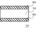
- FIG. 1 is a cross-sectional view showing an oscillation device 100 according to the first embodiment.
- the oscillation device 100 according to the present embodiment corresponds to the first invention in this specification.
- the oscillation device 100 according to the present embodiment includes a piezoelectric body 70, a plurality of upper electrodes 80, and a plurality of lower electrodes 82.
- the oscillation device 100 is mounted on an electronic device such as a mobile phone.
- the piezoelectric body 70 has a plurality of convex portions 72 on one surface.
- the plurality of upper electrodes 80 are provided separately from each other on the plurality of convex portions 72.
- the plurality of lower electrodes 82 are provided on the other surface opposite to the one surface of the piezoelectric body 70 so that each of them faces only one upper electrode 80.
- the configuration of the oscillation device 100 will be described in detail.
- FIG. 2 is a plan view showing the oscillation device 100 shown in FIG. FIG. 2 shows the top surface of the oscillation device 100.
- the convex part 72 and the upper electrode 80 provided on the convex part 72 are arranged in an array, for example.
- the piezoelectric body 70 has a plurality of convex portions 74 on the other surface, for example.
- the plurality of convex portions 74 are provided on the other surface of the piezoelectric body 70 so that each of the convex portions 74 overlaps with only one convex portion 72 in plan view.
- the plurality of convex portions 72 and the plurality of convex portions 74 are provided so as to be positioned symmetrically with respect to a central plane located between one surface and the other surface of the piezoelectric body 70. Yes (not shown).
- the piezoelectric body 70 is made of a material having a piezoelectric effect, for example, lead zirconate titanate (PZT) or barium titanate (BaTiO 3 ) as a material having high electromechanical conversion efficiency.
- the convex portion 72 and the convex portion 74 are formed by processing a piezoelectric body made of the above material having a piezoelectric effect. The processing of the piezoelectric body can be performed, for example, by cutting on a piezoelectric material or firing with a shape mold.
- the convex portion 72 and the convex portion 74 are, for example, square in plan view.
- the piezoelectric body 70 is polarized in the thickness direction (vertical direction in FIG. 1).
- the piezoelectric body 70 preferably has a thickness of 1 mm or less at a portion where the convex portion 72 and the convex portion 74 overlap in plan view. When the thickness exceeds 1 mm, the electric field strength of the piezoelectric body 70 is reduced. For this reason, the energy conversion efficiency is reduced.
- the piezoelectric body 70 preferably has a thickness of 10 ⁇ m or more in a portion where the convex portion 72 and the convex portion 74 are not located. When the thickness is less than 10 ⁇ m, the piezoelectric body 70 is made of a brittle material, and thus is easily damaged during handling.
- the upper electrode 80 can be provided, for example, so as to have the same shape as the convex portion 72 in plan view. Further, the lower electrode 82 can be provided so as to have the same shape as the convex portion 74 in a plan view, for example.
- the upper electrode 80 and the lower electrode 82 are made of a material having electrical conductivity, for example, silver or a silver / palladium alloy. Silver is a low-resistance general-purpose material and is advantageous from the viewpoint of manufacturing cost and manufacturing process. Further, the silver / palladium alloy is a low resistance material excellent in oxidation resistance and excellent in reliability.
- the thicknesses of the upper electrode 80 and the lower electrode 82 are preferably 1 to 50 ⁇ m.
- the thickness is less than 1 ⁇ m, it becomes difficult to form the film uniformly.
- the thickness exceeds 50 ⁇ m, the upper electrode 80 or the lower electrode 82 becomes a restraint surface with respect to the piezoelectric body 70 and causes a decrease in energy conversion efficiency.
- the upper electrode 80 and the lower electrode 82 facing each other, and the piezoelectric body 70 positioned therebetween constitute one piezoelectric vibrator 10. That is, one piezoelectric vibrator 10 is configured by the upper electrode 80 and the lower electrode 82 facing each other, and the convex portion 72 and the convex portion 74 positioned therebetween. Thereby, the oscillation device 100 has a plurality of piezoelectric vibrators 10.
- FIG. 3 is a plan view showing a modification of the oscillation device 100 shown in FIG.
- the convex part 72, the convex part 74, the upper electrode 80, and the lower electrode 82 have a square shape in plan view.
- the convex part 72, the convex part 74, the upper electrode 80, and the lower electrode 82 can select various shapes. For example, as shown in FIGS. 3A, 3 ⁇ / b> B, and 3 ⁇ / b> C, a rectangular shape can be provided.
- sequences is not limited. Further, as shown in FIG.
- the convex portion 72, the convex portion 74, the upper electrode 80, and the lower electrode 82 may be provided to have, for example, a circular or elliptical shape in plan view.
- the resonance frequencies of the plurality of piezoelectric vibrators 10 constituted by these can be selected.
- the interval between the piezoelectric vibrators 10 adjacent to each other can be arbitrarily set. Thereby, the interference of sound waves between the plurality of piezoelectric vibrators 10 can be suppressed.
- the oscillation device 100 includes a support frame 30 that holds a piezoelectric body 70, for example.
- the support frame 30 holds the edge of the piezoelectric body 70, for example. Further, the support frame 30 holds, for example, the entire circumference of the piezoelectric body 70.
- the oscillation device 100 includes a control unit 90 and a signal generation unit 92.
- the signal generator 92 is connected to each upper electrode 80 and each lower electrode 82. Then, an electric signal to be input to each piezoelectric vibrator 10 constituted by each upper electrode 80 and each lower electrode 82 is generated.
- the control unit 90 is connected to the signal generation unit 92 and controls signal generation by the signal generation unit 92.
- the control unit 90 controls the generation of signals from the signal generation unit 92 based on information input from the outside, so that the outputs of the plurality of piezoelectric vibrators 10 can be controlled independently of each other.
- each piezoelectric vibrator 10 uses a sound wave of 20 kHz or more, for example, 100 kHz, as a signal transport wave.
- the basic resonance frequency of the piezoelectric vibrator depends on the length of the contour shape of the vibration surface. That is, the area of the piezoelectric vibrator decreases as the resonance frequency shifts to a higher range. For this reason, the oscillation device 100 can be downsized by setting the oscillation frequency of each piezoelectric vibrator 10 to the ultrasonic band. Moreover, high directivity can also be realized by setting the oscillation frequency of each piezoelectric vibrator 10 to an ultrasonic band.
- the control unit 90 may input the audio signal as it is to each piezoelectric vibrator 10 via the signal generation unit 92.
- the signal input to the control unit 90 is a command signal for oscillating sound waves.
- the signal generation unit 92 causes each piezoelectric vibrator 10 to generate a sound wave having a resonance frequency of each piezoelectric vibrator 10.
- a plurality of upper electrodes 80 provided separately from each other on the plurality of convex portions 72 included in the piezoelectric body 70, and each of them faces only one upper electrode 80.
- a plurality of lower electrodes 82 provided on the other surface of the piezoelectric body 70.
- the plurality of convex portions 72, the plurality of upper electrodes 80 and the plurality of lower electrodes 82 constitute a plurality of piezoelectric vibrators 10.
- the plurality of piezoelectric vibrators 10 are composed of one layer of the piezoelectric body 70.
- the process which arranges the several piezoelectric vibrator 10 in an array form, and mutually joins is not required. Variations in characteristics among the plurality of piezoelectric vibrators 10 can be suppressed. Therefore, the acoustic characteristics of the electronic device can be improved.
- each piezoelectric vibrator 10 is controlled independently of each other via each upper electrode 80 and each lower electrode 82. For this reason, it becomes possible to control the plurality of piezoelectric vibrators 10 with a high degree of freedom.
- the plurality of piezoelectric vibrators 10 are constituted by the convex portions 72. That is, the plurality of piezoelectric vibrators 10 are arranged with a groove therebetween. Therefore, the vibration of the piezoelectric vibrator 10 is restrained from being restrained as compared with the case where no groove is formed between the piezoelectric vibrators 10. Therefore, energy loss of the oscillation device 100 can be suppressed and low power consumption can be achieved.
- the plurality of convex portions 72 are arranged with a groove interposed therebetween. For this reason, it is possible to prevent vibration from being transmitted from one piezoelectric vibrator 10 to another adjacent piezoelectric vibrator 10.
- FIG. 4 is a cross-sectional view showing an electronic device 200 according to the second embodiment.
- FIG. 5 is a plan view showing the electronic device 200 shown in FIG.
- the electronic device 200 according to the present embodiment corresponds to the second invention in this specification.
- the electronic device 200 according to the present embodiment includes a support member and a plurality of oscillation devices 100.
- the electronic device 200 is a mobile terminal device such as a mobile phone.
- the plurality of oscillation devices 100 are fixed on a support member.
- the oscillation device 100 includes a piezoelectric vibrator 10 and a vibration member 20.
- the vibration member 20 restrains the piezoelectric vibrator 10 on one surface.
- the vibration member 20 is bent at one end or the other surface opposite to the one surface. Further, the end portion of the vibration member 20 is held by the support member.
- the configuration of the electronic device 200 will be described in detail.
- the vibration member 20 has, for example, a flat plate shape.
- the vibration member 20 is made of a material having a high elastic modulus with respect to a ceramic that is a brittle material, such as metal or resin, and is made of a general-purpose material such as phosphor bronze or stainless steel.
- the thickness of the vibration member 20 is preferably 5 to 500 ⁇ m.
- the longitudinal elastic modulus of the vibration member 20 is preferably 1 to 500 GPa. When the longitudinal elastic modulus of the vibration member 20 is excessively low or high, the vibration characteristics and reliability of the oscillation device may be impaired.
- the vibration member 20 is held by a substrate 32, for example.
- the substrate 32 has a ring shape with a hollow inside.
- the ring shape is, for example, a quadrangle, but is not limited thereto, and may be a circle or an ellipse.
- the vibration member 20 is held on the substrate 32 by a part of the end portion being fixed on the substrate 32.
- substrate 32 is fixed by the support frame 30, for example.
- the end of the vibration member 20 is bent to one side.
- the vibration member 20 has a spring shape. For this reason, the plate spring effect acts on the vibration member 20 during vibration. Further, the stroke can be lengthened during vibration. Therefore, the sound pressure level of the oscillation device 100 can be improved.
- the vibration member 20 is bent to one surface side or the other surface at one end and the other end opposite to the one end. In the present embodiment, as shown in FIG. 4, one end and the other end of the vibration member 20 are both bent to one surface side.
- the vibration member 20 is fixed to the substrate 32 at one end and the other end.
- the vibrating member 20 is bent at the bent portion 22. Further, the end portion of the vibration member 20 is located on the inner side than 22 in a plan view. For this reason, the mounting area for the edge part of the bending vibration member 20 is not required. Therefore, the distance between the arranged oscillation devices 100 can be shortened and the electronic device 200 can be downsized.
- the plurality of oscillation devices 100 are disposed on both surfaces of the substrate 32, for example.
- a plurality of oscillation devices 102 are disposed on one surface of the substrate 32, and a plurality of oscillation devices 104 are disposed on the other surface. Further, the oscillation device 102 and the oscillation device 104 are arranged so as to be shifted from each other in plan view.
- the oscillation device 102 and the oscillation device 104 are arranged at positions shifted from each other in plan view.
- the substrate 32 has a ring shape with a hollow inside. For this reason, on one surface side of the substrate 32, sound waves output from the plurality of oscillation devices 102 to the one surface side of the substrate 32 and gaps between the plurality of oscillation devices 104 to the oscillation device 102 pass to the one surface side of the substrate 32. The outputted sound wave is emitted. Further, on the other surface side of the substrate 32, sound waves output from the plurality of oscillation devices 104 to the other surface side of the substrate 32 and the other surface of the substrate 32 through the gaps between the plurality of oscillation devices 102 and the oscillation device 104.
- Sound waves output to the side are emitted. Therefore, sound waves output from the oscillation device 102 and the oscillation device 104 are efficiently radiated, and a high sound pressure level can be realized. Note that the arrangement of the oscillation device 102 and the oscillation device 104 can be arbitrarily adjusted.
- FIG. 6 is a cross-sectional view showing the piezoelectric vibrator 10 shown in FIG.
- the piezoelectric vibrator 10 includes a piezoelectric body 70, an upper electrode 80, and a lower electrode 82.
- the piezoelectric body 70 is sandwiched between the upper electrode 80 and the lower electrode 82.
- the piezoelectric body 70 is polarized in the thickness direction (vertical direction in FIG. 6).
- the piezoelectric vibrator 10 has, for example, a circle or an ellipse in a plane direction parallel to one surface of the vibration member 20.
- the piezoelectric body 70 for example, the same one as in the first embodiment can be used.
- the upper electrode 80 and the lower electrode 82 the thing similar to 1st Embodiment can be used, for example.
- the electronic device 200 includes a control unit 90 and a signal generation unit 92.
- the signal generator 92 is connected to each piezoelectric vibrator 10 and generates an electric signal to be input to each piezoelectric vibrator 10.
- the control unit 90 is connected to the signal generation unit 92 and controls signal generation by the signal generation unit 92.
- the control unit 90 controls the generation of the signal of the signal generation unit 92 based on information input from the outside, whereby the outputs of the plurality of oscillation devices 100 can be controlled independently of each other.
- the output control of the oscillation device 100 can be performed using the control unit 90 and the signal generation unit 92 as in the first embodiment.
- the electronic device 200 includes a vibration member that restrains the piezoelectric vibrator 10 on one surface, is bent at one end or the other surface, and is held by a support member at the end. .
- the vibration member 20 has a spring shape. For this reason, the plate spring effect acts on the vibration member 20 during vibration. Further, the stroke can be lengthened during vibration. Thereby, the sound pressure level of the oscillation device 100 can be improved. Therefore, the acoustic characteristics of the electronic device can be improved.
Priority Applications (4)
| Application Number | Priority Date | Filing Date | Title |
|---|---|---|---|
| CN201280015185.2A CN103444207B (zh) | 2011-03-31 | 2012-03-08 | 振荡器和电子设备 |
| US14/008,383 US9252711B2 (en) | 2011-03-31 | 2012-03-08 | Oscillator and electronic device |
| EP12763576.1A EP2693771B1 (de) | 2011-03-31 | 2012-03-08 | Oszillator und elektronische vorrichtung |
| JP2013507125A JP6024655B2 (ja) | 2011-03-31 | 2012-03-08 | 発振装置、および電子機器 |
Applications Claiming Priority (2)
| Application Number | Priority Date | Filing Date | Title |
|---|---|---|---|
| JP2011-081025 | 2011-03-31 | ||
| JP2011081025 | 2011-03-31 |
Publications (1)
| Publication Number | Publication Date |
|---|---|
| WO2012132261A1 true WO2012132261A1 (ja) | 2012-10-04 |
Family
ID=46930056
Family Applications (1)
| Application Number | Title | Priority Date | Filing Date |
|---|---|---|---|
| PCT/JP2012/001603 WO2012132261A1 (ja) | 2011-03-31 | 2012-03-08 | 発振装置、および電子機器 |
Country Status (5)
| Country | Link |
|---|---|
| US (1) | US9252711B2 (de) |
| EP (2) | EP2908554B1 (de) |
| JP (1) | JP6024655B2 (de) |
| CN (1) | CN103444207B (de) |
| WO (1) | WO2012132261A1 (de) |
Cited By (1)
| Publication number | Priority date | Publication date | Assignee | Title |
|---|---|---|---|---|
| JP2019176350A (ja) * | 2018-03-28 | 2019-10-10 | 株式会社Soken | パラメトリックスピーカ |
Families Citing this family (2)
| Publication number | Priority date | Publication date | Assignee | Title |
|---|---|---|---|---|
| US9996199B2 (en) * | 2012-07-10 | 2018-06-12 | Electronics And Telecommunications Research Institute | Film haptic system having multiple operation points |
| US10915881B2 (en) | 2017-01-27 | 2021-02-09 | American Express Travel Related Services Company, Inc. | Transaction account charge splitting |
Citations (13)
| Publication number | Priority date | Publication date | Assignee | Title |
|---|---|---|---|---|
| JPS6210594U (de) | 1985-07-04 | 1987-01-22 | ||
| JPS62148000U (de) | 1986-03-12 | 1987-09-18 | ||
| JPH04111599A (ja) * | 1990-08-30 | 1992-04-13 | Nippon Dempa Kogyo Co Ltd | 超音波探触子 |
| JPH0541899A (ja) | 1991-08-05 | 1993-02-19 | Fujitsu Ltd | 超音波探触子 |
| JPH0575372A (ja) | 1991-09-10 | 1993-03-26 | Murata Mfg Co Ltd | 圧電共振子及びその製造方法 |
| JPH07163166A (ja) | 1993-12-03 | 1995-06-23 | Seiko Instr Inc | 圧電アクチュエータ及びその製造方法 |
| JPH0984193A (ja) | 1995-09-07 | 1997-03-28 | Denso Corp | 複合圧電材の製造方法 |
| JP2004349817A (ja) * | 2003-05-20 | 2004-12-09 | Seiko Epson Corp | パラメトリックスピーカ |
| WO2005094121A1 (ja) | 2004-03-25 | 2005-10-06 | Nec Corporation | 圧電音響素子、音響装置及び携帯端末装置 |
| JP2005286690A (ja) * | 2004-03-30 | 2005-10-13 | Mitsubishi Electric Engineering Co Ltd | 圧電膜スピーカ及びそれを用いたパラメトリックスピーカ |
| JP2006332616A (ja) | 2005-04-28 | 2006-12-07 | Brother Ind Ltd | 圧電アクチュエータの製造方法 |
| JP2007307288A (ja) * | 2006-05-22 | 2007-11-29 | Fujifilm Corp | 曲面貼着方法および超音波プローブ |
| JP2008118212A (ja) * | 2006-10-31 | 2008-05-22 | Toshiba Corp | 超音波プローブおよび超音波診断装置 |
Family Cites Families (12)
| Publication number | Priority date | Publication date | Assignee | Title |
|---|---|---|---|---|
| US3878477A (en) * | 1974-01-08 | 1975-04-15 | Hewlett Packard Co | Acoustic surface wave oscillator force-sensing devices |
| US4281550A (en) * | 1979-12-17 | 1981-08-04 | North American Philips Corporation | Curved array of sequenced ultrasound transducers |
| US4550606A (en) | 1982-09-28 | 1985-11-05 | Cornell Research Foundation, Inc. | Ultrasonic transducer array with controlled excitation pattern |
| JPH0660896B2 (ja) * | 1984-11-02 | 1994-08-10 | 株式会社日立製作所 | 超音波探触子 |
| US4870867A (en) | 1988-12-27 | 1989-10-03 | North American Philips Corp. | Crossed linear arrays for ultrasonic medical imaging |
| JP3967140B2 (ja) * | 2001-09-18 | 2007-08-29 | 大成プラス株式会社 | 携帯通信装置 |
| US7412764B2 (en) * | 2002-03-06 | 2008-08-19 | Piedek Technical Laboratory | Method for manufacturing quartz crystal unit and electronic apparatus having quartz crystal unit |
| AU2003304673A1 (en) | 2003-11-27 | 2005-06-17 | Seung-Hwan Yi | Piezoelectric microspeaker with corrugated diaphragm |
| US7227295B2 (en) * | 2005-02-04 | 2007-06-05 | Asm Assembly Automation Ltd. | Piezoelectric device with amplifying mechanism |
| CN101262959A (zh) * | 2005-08-31 | 2008-09-10 | 日本电气株式会社 | 压电致动器、声学部件、以及电子装置 |
| US7564316B2 (en) * | 2005-12-23 | 2009-07-21 | Avago Technologies Wireless Ip (Singapore) Pte. Ltd. | Variable-frequency oscillator incorporating thin-film bulk acoustic resonators |
| JP4869391B2 (ja) | 2009-10-02 | 2012-02-08 | シャープ株式会社 | 電子写真感光体及びそれを備えた画像形成装置 |
-
2012
- 2012-03-08 CN CN201280015185.2A patent/CN103444207B/zh not_active Expired - Fee Related
- 2012-03-08 EP EP15155345.0A patent/EP2908554B1/de not_active Not-in-force
- 2012-03-08 US US14/008,383 patent/US9252711B2/en not_active Expired - Fee Related
- 2012-03-08 WO PCT/JP2012/001603 patent/WO2012132261A1/ja active Application Filing
- 2012-03-08 JP JP2013507125A patent/JP6024655B2/ja not_active Expired - Fee Related
- 2012-03-08 EP EP12763576.1A patent/EP2693771B1/de not_active Not-in-force
Patent Citations (13)
| Publication number | Priority date | Publication date | Assignee | Title |
|---|---|---|---|---|
| JPS6210594U (de) | 1985-07-04 | 1987-01-22 | ||
| JPS62148000U (de) | 1986-03-12 | 1987-09-18 | ||
| JPH04111599A (ja) * | 1990-08-30 | 1992-04-13 | Nippon Dempa Kogyo Co Ltd | 超音波探触子 |
| JPH0541899A (ja) | 1991-08-05 | 1993-02-19 | Fujitsu Ltd | 超音波探触子 |
| JPH0575372A (ja) | 1991-09-10 | 1993-03-26 | Murata Mfg Co Ltd | 圧電共振子及びその製造方法 |
| JPH07163166A (ja) | 1993-12-03 | 1995-06-23 | Seiko Instr Inc | 圧電アクチュエータ及びその製造方法 |
| JPH0984193A (ja) | 1995-09-07 | 1997-03-28 | Denso Corp | 複合圧電材の製造方法 |
| JP2004349817A (ja) * | 2003-05-20 | 2004-12-09 | Seiko Epson Corp | パラメトリックスピーカ |
| WO2005094121A1 (ja) | 2004-03-25 | 2005-10-06 | Nec Corporation | 圧電音響素子、音響装置及び携帯端末装置 |
| JP2005286690A (ja) * | 2004-03-30 | 2005-10-13 | Mitsubishi Electric Engineering Co Ltd | 圧電膜スピーカ及びそれを用いたパラメトリックスピーカ |
| JP2006332616A (ja) | 2005-04-28 | 2006-12-07 | Brother Ind Ltd | 圧電アクチュエータの製造方法 |
| JP2007307288A (ja) * | 2006-05-22 | 2007-11-29 | Fujifilm Corp | 曲面貼着方法および超音波プローブ |
| JP2008118212A (ja) * | 2006-10-31 | 2008-05-22 | Toshiba Corp | 超音波プローブおよび超音波診断装置 |
Non-Patent Citations (1)
| Title |
|---|
| See also references of EP2693771A4 |
Cited By (1)
| Publication number | Priority date | Publication date | Assignee | Title |
|---|---|---|---|---|
| JP2019176350A (ja) * | 2018-03-28 | 2019-10-10 | 株式会社Soken | パラメトリックスピーカ |
Also Published As
| Publication number | Publication date |
|---|---|
| US9252711B2 (en) | 2016-02-02 |
| EP2908554B1 (de) | 2017-09-06 |
| JP6024655B2 (ja) | 2016-11-16 |
| CN103444207B (zh) | 2016-08-31 |
| EP2693771A1 (de) | 2014-02-05 |
| JPWO2012132261A1 (ja) | 2014-07-24 |
| EP2908554A1 (de) | 2015-08-19 |
| EP2693771B1 (de) | 2016-02-03 |
| EP2693771A4 (de) | 2014-09-24 |
| CN103444207A (zh) | 2013-12-11 |
| US20140015617A1 (en) | 2014-01-16 |
Similar Documents
| Publication | Publication Date | Title |
|---|---|---|
| CN102986249A (zh) | 振荡器和电子设备 | |
| JP5652813B2 (ja) | 電気音響変換器及びそれを用いた電子機器 | |
| US9392375B2 (en) | Acoustic generator, acoustic generation device, and electronic device | |
| JP5939160B2 (ja) | 発振装置および電子機器 | |
| JP6024655B2 (ja) | 発振装置、および電子機器 | |
| CN106448641B (zh) | 压电模块 | |
| JP6442531B2 (ja) | 音響発生器、音響発生装置及び電子機器 | |
| JPWO2014045719A1 (ja) | 音響発生器、音響発生装置及び電子機器 | |
| KR101765000B1 (ko) | 지향성 스피커용 압전 트랜스듀서 및 이를 포함하는 지향성 스피커 | |
| JP6567911B2 (ja) | 音響発生器およびこれを備えた音響発生装置、電子機器 | |
| EP2693772B1 (de) | Oszillator | |
| JP2012029110A (ja) | 発振装置 | |
| JPWO2016067667A1 (ja) | 音響発生器、音響発生装置および電子機器 | |
| JP2012217036A (ja) | 発振装置、および電子機器 | |
| JP5871753B2 (ja) | 音響発生器、音響発生装置および電子機器 | |
| JP2012217037A (ja) | 電子機器 | |
| JP5488266B2 (ja) | 発振装置 | |
| JP6431086B2 (ja) | 圧電素子、音響発生器、音響発生装置および電子機器 | |
| JP2012134599A (ja) | 発振装置および電子機器 | |
| JP2012217041A (ja) | 電子機器 | |
| JP2012217040A (ja) | 発振装置、および携帯端末装置 | |
| JP2012217031A (ja) | 発振装置、および電子機器 | |
| JP2012142652A (ja) | 発振装置 | |
| JP2015019188A (ja) | 圧電型電気音響変換器及び電子機器 | |
| JP2014239386A (ja) | 圧電型電気音響変換器及び電子機器 |
Legal Events
| Date | Code | Title | Description |
|---|---|---|---|
| 121 | Ep: the epo has been informed by wipo that ep was designated in this application |
Ref document number: 12763576 Country of ref document: EP Kind code of ref document: A1 |
|
| WWE | Wipo information: entry into national phase |
Ref document number: 2012763576 Country of ref document: EP |
|
| ENP | Entry into the national phase |
Ref document number: 2013507125 Country of ref document: JP Kind code of ref document: A |
|
| WWE | Wipo information: entry into national phase |
Ref document number: 14008383 Country of ref document: US |
|
| NENP | Non-entry into the national phase |
Ref country code: DE |