WO2012132219A1 - 半導体装置及びその製造方法 - Google Patents
半導体装置及びその製造方法 Download PDFInfo
- Publication number
- WO2012132219A1 WO2012132219A1 PCT/JP2012/001285 JP2012001285W WO2012132219A1 WO 2012132219 A1 WO2012132219 A1 WO 2012132219A1 JP 2012001285 W JP2012001285 W JP 2012001285W WO 2012132219 A1 WO2012132219 A1 WO 2012132219A1
- Authority
- WO
- WIPO (PCT)
- Prior art keywords
- semiconductor layer
- layer
- mosfet
- semiconductor device
- resistance substrate
- Prior art date
- Legal status (The legal status is an assumption and is not a legal conclusion. Google has not performed a legal analysis and makes no representation as to the accuracy of the status listed.)
- Ceased
Links
Images









Classifications
-
- H—ELECTRICITY
- H10—SEMICONDUCTOR DEVICES; ELECTRIC SOLID-STATE DEVICES NOT OTHERWISE PROVIDED FOR
- H10D—INORGANIC ELECTRIC SEMICONDUCTOR DEVICES
- H10D62/00—Semiconductor bodies, or regions thereof, of devices having potential barriers
- H10D62/10—Shapes, relative sizes or dispositions of the regions of the semiconductor bodies; Shapes of the semiconductor bodies
- H10D62/124—Shapes, relative sizes or dispositions of the regions of semiconductor bodies or of junctions between the regions
- H10D62/126—Top-view geometrical layouts of the regions or the junctions
-
- H—ELECTRICITY
- H10—SEMICONDUCTOR DEVICES; ELECTRIC SOLID-STATE DEVICES NOT OTHERWISE PROVIDED FOR
- H10D—INORGANIC ELECTRIC SEMICONDUCTOR DEVICES
- H10D30/00—Field-effect transistors [FET]
- H10D30/60—Insulated-gate field-effect transistors [IGFET]
-
- H—ELECTRICITY
- H10—SEMICONDUCTOR DEVICES; ELECTRIC SOLID-STATE DEVICES NOT OTHERWISE PROVIDED FOR
- H10D—INORGANIC ELECTRIC SEMICONDUCTOR DEVICES
- H10D62/00—Semiconductor bodies, or regions thereof, of devices having potential barriers
- H10D62/10—Shapes, relative sizes or dispositions of the regions of the semiconductor bodies; Shapes of the semiconductor bodies
- H10D62/113—Isolations within a component, i.e. internal isolations
- H10D62/115—Dielectric isolations, e.g. air gaps
- H10D62/116—Dielectric isolations, e.g. air gaps adjoining the input or output regions of field-effect devices, e.g. adjoining source or drain regions
-
- H—ELECTRICITY
- H10—SEMICONDUCTOR DEVICES; ELECTRIC SOLID-STATE DEVICES NOT OTHERWISE PROVIDED FOR
- H10D—INORGANIC ELECTRIC SEMICONDUCTOR DEVICES
- H10D86/00—Integrated devices formed in or on insulating or conducting substrates, e.g. formed in silicon-on-insulator [SOI] substrates or on stainless steel or glass substrates
- H10D86/01—Manufacture or treatment
-
- H—ELECTRICITY
- H10—SEMICONDUCTOR DEVICES; ELECTRIC SOLID-STATE DEVICES NOT OTHERWISE PROVIDED FOR
- H10D—INORGANIC ELECTRIC SEMICONDUCTOR DEVICES
- H10D86/00—Integrated devices formed in or on insulating or conducting substrates, e.g. formed in silicon-on-insulator [SOI] substrates or on stainless steel or glass substrates
- H10D86/201—Integrated devices formed in or on insulating or conducting substrates, e.g. formed in silicon-on-insulator [SOI] substrates or on stainless steel or glass substrates the substrates comprising an insulating layer on a semiconductor body, e.g. SOI
-
- H—ELECTRICITY
- H10—SEMICONDUCTOR DEVICES; ELECTRIC SOLID-STATE DEVICES NOT OTHERWISE PROVIDED FOR
- H10D—INORGANIC ELECTRIC SEMICONDUCTOR DEVICES
- H10D87/00—Integrated devices comprising both bulk components and either SOI or SOS components on the same substrate
-
- H—ELECTRICITY
- H10—SEMICONDUCTOR DEVICES; ELECTRIC SOLID-STATE DEVICES NOT OTHERWISE PROVIDED FOR
- H10P—GENERIC PROCESSES OR APPARATUS FOR THE MANUFACTURE OR TREATMENT OF DEVICES COVERED BY CLASS H10
- H10P90/00—Preparation of wafers not covered by a single main group of this subclass, e.g. wafer reinforcement
- H10P90/19—Preparing inhomogeneous wafers
- H10P90/1904—Preparing vertically inhomogeneous wafers
- H10P90/1906—Preparing SOI wafers
-
- H—ELECTRICITY
- H10—SEMICONDUCTOR DEVICES; ELECTRIC SOLID-STATE DEVICES NOT OTHERWISE PROVIDED FOR
- H10W—GENERIC PACKAGES, INTERCONNECTIONS, CONNECTORS OR OTHER CONSTRUCTIONAL DETAILS OF DEVICES COVERED BY CLASS H10
- H10W10/00—Isolation regions in semiconductor bodies between components of integrated devices
- H10W10/01—Manufacture or treatment
- H10W10/011—Manufacture or treatment of isolation regions comprising dielectric materials
- H10W10/014—Manufacture or treatment of isolation regions comprising dielectric materials using trench refilling with dielectric materials, e.g. shallow trench isolations
-
- H—ELECTRICITY
- H10—SEMICONDUCTOR DEVICES; ELECTRIC SOLID-STATE DEVICES NOT OTHERWISE PROVIDED FOR
- H10W—GENERIC PACKAGES, INTERCONNECTIONS, CONNECTORS OR OTHER CONSTRUCTIONAL DETAILS OF DEVICES COVERED BY CLASS H10
- H10W10/00—Isolation regions in semiconductor bodies between components of integrated devices
- H10W10/01—Manufacture or treatment
- H10W10/061—Manufacture or treatment using SOI processes together with lateral isolation, e.g. combinations of SOI and shallow trench isolations
-
- H—ELECTRICITY
- H10—SEMICONDUCTOR DEVICES; ELECTRIC SOLID-STATE DEVICES NOT OTHERWISE PROVIDED FOR
- H10W—GENERIC PACKAGES, INTERCONNECTIONS, CONNECTORS OR OTHER CONSTRUCTIONAL DETAILS OF DEVICES COVERED BY CLASS H10
- H10W10/00—Isolation regions in semiconductor bodies between components of integrated devices
- H10W10/10—Isolation regions comprising dielectric materials
- H10W10/17—Isolation regions comprising dielectric materials formed using trench refilling with dielectric materials, e.g. shallow trench isolations
-
- H—ELECTRICITY
- H10—SEMICONDUCTOR DEVICES; ELECTRIC SOLID-STATE DEVICES NOT OTHERWISE PROVIDED FOR
- H10W—GENERIC PACKAGES, INTERCONNECTIONS, CONNECTORS OR OTHER CONSTRUCTIONAL DETAILS OF DEVICES COVERED BY CLASS H10
- H10W10/00—Isolation regions in semiconductor bodies between components of integrated devices
- H10W10/10—Isolation regions comprising dielectric materials
- H10W10/181—Semiconductor-on-insulator [SOI] isolation regions, e.g. buried oxide regions of SOI wafers
Definitions
- the present invention relates to a semiconductor device and a manufacturing method thereof, and more particularly to a semiconductor device in which a plurality of types of elements are mixedly mounted and a manufacturing method thereof.
- silicon MOSFETs Metal-Oxide-Semiconductor Field-Effect Transistors
- SOI Silicon-on-Insulator
- SOS Silicon-on-Sapphire
- Important characteristics that indicate the performance of a high-frequency switch include transmission loss, harmonic distortion, and inter-modulation distortion (IMD). These characteristics can be improved as the CR product, which is the product of the parasitic capacitance C and the on-resistance R, of the MOSFET is reduced.
- IMD inter-modulation distortion
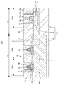
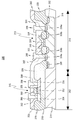
- FIG. 5 is a cross-sectional view showing a configuration of a general semiconductor device 300 in which a MOSFET is formed on an SOI substrate.
- the SOI substrate includes a p-type silicon substrate 314.
- the silicon substrate 314 has a first region 310 and a second region 312.
- a high breakdown voltage transistor 313 is formed in the first region 310.
- Other semiconductor elements that can be formed in the first region 310 include vertical bipolar.
- a MOS field effect transistor 315 having an SOI structure is formed in the second region 312.
- the high breakdown voltage transistor 313 includes a gate electrode 340, source / drains 334a and 336a, and source / drain offsets 334b and 336b.
- a p-type well 316 is formed in the silicon substrate 314 in the first region 310.
- a gate oxide film 338 is formed on the well 316. The thickness of the gate oxide film 338 is, for example, 40 to 100 nm.
- Offset LOCOS oxide films 322 and 324 are formed on the well 316 with the gate oxide film 338 interposed therebetween.
- a gate electrode 340 is formed on the gate oxide film 338. One end of the gate electrode 340 is located on the offset LOCOS oxide film 322. The other end of the gate electrode 340 is located on the offset LOCOS oxide film 324.
- an n-type source / drain offset 334b is formed in the well 316 under the offset LOCOS oxide film 322.
- an n-type source / drain offset 334a is formed in the well 316.
- the n-type source / drain 334a is located next to the source / drain offset 334b.
- An n-type source / drain offset 336 b is formed in the well 316 under the offset LOCOS oxide film 324.
- an n-type source / drain 336a is formed in the well 316 under the offset LOCOS oxide film 324.
- an n-type source / drain 336a is formed in the well 316 under the offset LOCOS oxide film 324.
- an n-type source / drain 336a is formed in the well 316 under the offset LOCOS oxide film 324.
- an n-type source / drain 336a is formed in the well 316 under the offset LOCOS oxide film 324.
- the element isolation LOCOS oxide film 326 is formed at one end of the well 316, and the element isolation LOCOS oxide film 320 is formed at the other end of the well 316.
- a p-type channel stopper region 330 is formed in the well 316 under the element isolation LOCOS oxide film 326.
- a p-type channel stopper region 332 is formed in the well 316 under the LOCOS oxide film 320.
- An interlayer insulating film 350 is formed on the silicon substrate 314 so as to cover the gate electrode 340.
- a through hole 342 exposing the source / drain 334a is formed in the interlayer insulating film 350.
- An aluminum wiring 346 is formed on the interlayer insulating film 350.
- Aluminum wiring 346 is also formed in through hole 342 and is electrically connected to source / drain 334a.
- a through hole 344 exposing the source / drain 336a is formed in the interlayer insulating film 350.
- An aluminum wiring 348 is formed on the interlayer insulating film 350. The aluminum wiring 348 is also formed in the through hole 344 and is electrically connected to the source / drain 336a.
- the MOS field effect transistor 315 includes a gate electrode 360 and source / drains 354 and 356.
- a buried oxide film 318 is formed on the silicon substrate 314 in the second region 312.
- a silicon single crystal layer is formed on the buried oxide film 318.
- a p-type body region 352 and n-type source / drains 354 and 356 are formed in the silicon single crystal layer.
- Element isolation LOCOS oxide films 326 and 328 are formed on the buried oxide film 318.
- the MOS field effect transistor 315 is insulated and isolated from other elements by the element isolation LOCOS oxide films 326 and 328.
- a gate oxide film 358 is formed on the body region 352.
- the thickness of the gate oxide film 358 is, for example, 3 to 10 nm.
- An interlayer insulating film 350 is formed on the silicon substrate 314 so as to cover the gate electrode 360.
- a through hole 362 exposing the source / drain 354 is formed in the interlayer insulating film 350.
- An aluminum wiring 366 is formed on the interlayer insulating film 350. The aluminum wiring 366 is also formed in the through hole 362 and is electrically connected to the source / drain 354.
- a through hole 364 exposing the source / drain 356 is formed in the interlayer insulating film 350.
- An aluminum wiring 368 is formed on the interlayer insulating film 350. The aluminum wiring 368 is also formed in the through hole 364 and is electrically connected to the source / drain 356.
- a high voltage MOSFET that requires a deep diffusion layer and a MOSFET having an SOI structure can be formed on the same substrate.
- Patent Document 2 a drive circuit that can easily control the slew rate while suppressing the circuit size has been proposed. Also, examples of the same type of semiconductor device are presented (Patent Documents 3 and 4).
- JP 2001-7219 A Japanese Patent Laid-Open No. 8-102498 JP 2008-227084 A JP 2007-201240 A
- the semiconductor device described above has the following problems.
- a MOSFET having an SOI structure is required to reduce the parasitic capacitance or to suppress the influence of a support substrate when used for high frequency applications. Therefore, it is necessary to form a thick buried oxide film (BOX) layer.
- BOX buried oxide film
- a high step is generated between the SOI substrate and the BOX layer and the support substrate as in the semiconductor device 300 shown in FIG.
- a focus shift due to a step occurs, and the dimensional accuracy of the device deteriorates.
- the generation of a film residue at the step portion in the dry etching process and the complicated etching conditions are caused. Therefore, in the above-described semiconductor device, it is inevitable that the device that can be manufactured is limited and the yield is reduced.
- a semiconductor device includes a first MOSFET formed on a high-resistance substrate, and a second MOSFET monolithically integrated with the first MOSFET on the high-resistance substrate,
- the first MOSFET is a first semiconductor layer formed on the high-resistance substrate, and a second semiconductor which is a well layer of the first MOSFET formed on the first semiconductor layer.
- the second MOSFET is formed on the high-resistance substrate and sandwiched between two trenches so that the upper part has a mesa shape, and the upper surface of the mesa shape is the first semiconductor layer.
- a semiconductor device includes a first MOSFET formed on a high-resistance substrate, and a second MOSFET monolithically integrated with the first MOSFET on the high-resistance substrate,
- the first MOSFET is a first semiconductor layer formed on the high-resistance substrate, and a second semiconductor which is a well layer of the first MOSFET formed on the first semiconductor layer.
- the second MOSFET has a trench formed in the first semiconductor layer formed on the high-resistance substrate, and is then oxidized from the side and bottom surfaces of the trench so that the upper portion of the second MOSFET is A first insulating layer having a mesa shape sandwiched between two trenches, a second insulating layer formed on the mesa shape of the first insulating layer, and formed on the second insulating layer
- the second A third semiconductor layer which is of the MOSFET well layer, those comprising a.
- a first semiconductor layer is formed over the high-resistance substrate, a second insulating layer is formed over the first semiconductor layer, and the second A third semiconductor layer to be a well layer of the second MOSFET is formed on the insulating layer, the second insulating layer and the third semiconductor layer in the first region are removed, and the second region An opening is formed in the second insulating layer and the third semiconductor layer, and the first of the opening formed in the second insulating layer and the third semiconductor layer in the second region.
- a first insulating layer having an upper portion having a mesa shape is formed between the first semiconductor layer and the second semiconductor layer serving as a well layer of the first MOSFET in the upper portion of the first semiconductor layer in the first region. Is formed. Thereby, even if the first insulating layer is formed, the first insulating layer does not protrude above the second semiconductor layer, and the step generated between the first and second MOSFETs is suppressed. can do.
- the present invention it is possible to provide a semiconductor device capable of suitably monolithically integrating transistors formed on an insulating layer and a manufacturing method thereof.
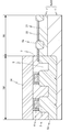
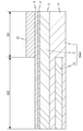
- FIG. 1 is a cross-sectional view schematically showing a configuration of a semiconductor device 100 according to a first embodiment.
- 4 is a cross-sectional view schematically showing a method for manufacturing the semiconductor device 100 according to the first embodiment.
- FIG. 4 is a cross-sectional view schematically showing a method for manufacturing the semiconductor device 100 according to the first embodiment.
- FIG. 4 is a cross-sectional view schematically showing a method for manufacturing the semiconductor device 100 according to the first embodiment.
- FIG. 4 is a cross-sectional view schematically showing a method for manufacturing the semiconductor device 100 according to the first embodiment.
- FIG. 4 is a cross-sectional view schematically showing a method for manufacturing the semiconductor device 100 according to the first embodiment.
- FIG. 4 is a cross-sectional view schematically showing a method for manufacturing the semiconductor device 100 according to the first embodiment.
- FIG. 4 is a cross-sectional view schematically showing a method for manufacturing the semiconductor device 100 according to the first embodiment.
- FIG. 4 is a cross-sectional view schematically showing a method for manufacturing the semiconductor device 100 according to the first embodiment.
- FIG. 4 is a cross-sectional view schematically showing a method for manufacturing the semiconductor device 100 according to the first embodiment.
- FIG. 4 is a cross-sectional view schematically showing a method for manufacturing the semiconductor device 100 according to the first embodiment.
- FIG. 4 is a cross-sectional view schematically showing a method for manufacturing the semiconductor device 100 according to the first embodiment.
- FIG. 4 is a cross-sectional view schematically showing a method for manufacturing the semiconductor device 100 according to the first embodiment.
- FIG. 4 is a cross-sectional view schematically showing a method for manufacturing the semiconductor device 100 according to the first embodiment.
- FIG. 4 is a cross-sectional view schematically showing a method for manufacturing the semiconductor device 100 according to the first embodiment.
- FIG. 4 is a cross-sectional view schematically showing a method for manufacturing the semiconductor device 100 according to the first embodiment.
- FIG. 4 is a cross-sectional view schematically showing a method for manufacturing the semiconductor device 100 according to the first embodiment.
- FIG. 4 is a cross-sectional view schematically showing a method for manufacturing the semiconductor device 100 according to the first embodiment.
- FIG. 4 is a cross-sectional view schematically showing a method for manufacturing the semiconductor device 100 according to the first embodiment.
- FIG. FIG. 6 is a cross-sectional view schematically showing a method for manufacturing the semiconductor device 200 according to the second embodiment.
- FIG. 10 is a cross-sectional view schematically showing a method for manufacturing the substrate Sub2 of the semiconductor device 200 according to the second embodiment.
- FIG. 10 is a cross-sectional view schematically showing a method for manufacturing the substrate Sub2 of the semiconductor device 200 according to the second embodiment.
- 3 is a cross-sectional view schematically showing a configuration of a semiconductor device 300.
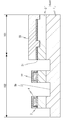
- FIG. 1 is a cross-sectional view schematically showing the configuration of the semiconductor device 100 according to the first embodiment.
- the semiconductor device 100 includes a logic circuit region 101 and a switch circuit region 102 monolithically integrated on the high resistance substrate 1.
- a logic MOSFET 101a is formed in the logic circuit region 101.
- a switch circuit region 102 switching MOSFETs 102a and 102b are formed.
- the epitaxial layer 2 is formed on the high resistance substrate 1.
- a LOCOS oxide film 6a which is an insulating layer, is formed on the epitaxial layer 2.
- a well layer 8 made of, for example, p-type silicon is formed between the two LOCOS oxide films 6a.
- the logic MOSFET 101 a is formed on the well layer 8. The portions of the epitaxial layer 2 and the LOCOS oxide film 6a where the well layer 8 is not formed are covered with the gate oxide film 9a.
- the configuration of the logic MOSFET 101a will be described.
- two n-type diffusion layers 12 a are formed on the well layer 8.
- the two diffusion layers 12a are the source and drain of the logic MOSFET 101a, respectively.
- a gate oxide film 9a which is an insulating layer, is formed between the well layer 8 between the two diffusion layers 12a and the gate electrode 10a.
- the gate electrode 10a is made of, for example, polysilicon, and the gate oxide film 9a is made of a silicon oxide film.
- a silicide 13a is formed on the gate electrode 10a.
- a silicide 13b is formed on the diffusion layer 12a.
- the side wall of the gate electrode 10 a is covered with the side wall 11.
- An interlayer insulating film 14 covering the logic MOSFET 101a is formed. Contact holes are formed in the interlayer insulating film 14 on the silicides 13a and 13b.
- a LOCOS oxide film 6b which is an insulating layer, is formed on the high resistance substrate 1.
- the LOCOS oxide film 6b is provided with a trench 5. Thereby, the upper part of the LOCOC oxide film sandwiched between the trenches 5 has a mesa shape.
- the trench 5 is filled with an oxide film 7.
- a buried oxide film 3 (thickness of 0.1 to 0.4 ⁇ m) and an SOI layer 4 (thickness of 0.1 ⁇ m or less) are formed on the LOCOS oxide film 6b.
- the buried oxide film 3 which is an insulating layer is made of, for example, silicon oxide
- the SOI layer 4 is made of, for example, silicon.
- a diffusion layer 12 b is formed on the SOI layer 4.
- the two diffusion layers 12b are a source and a drain of the switching MOSFET 102a, respectively.
- a gate oxide film 9b which is an insulating layer, is formed between the upper surface of the SOI layer 4 and the gate electrode 10b.
- the gate electrode 10b is made of, for example, polysilicon, and the gate oxide film 9b is made of silicon oxide.
- a silicide 13c is formed on the gate electrode 10b.
- a silicide 13d is formed on the diffusion layer 12b.
- the side wall of the gate electrode 10 b is covered with the sidewall 11.
- An interlayer insulating film 14 is formed to cover the switching MOSFET 102a. Contact holes are formed in the interlayer insulating film 14 on the silicides 13c and 13d. Note that the configuration of the switching MOSFET 102b is the same as that of the switching MOSFET 102a, and thus the description thereof is omitted.
- the logic circuit area 101 corresponds to the first area
- the switch circuit area 102 corresponds to the second area
- the logic MOSFET 101a corresponds to the first MOSFET
- the switching MOSFETs 102a and 102b correspond to the second MOSFET.
- the epitaxial layer 2, the well layer 8, the SOI layer 4, and the interface carrier suppression layer 15 correspond to first to fourth semiconductor layers, respectively.
- the LOCOS oxide film 6b and the buried oxide film 3 correspond to first and second oxide films, respectively.
- Gate oxide films 9a and 9b correspond to first and second gate insulating films, respectively.
- the diffusion layer 12a corresponds to the first and second diffusion layers.
- the diffusion layer 12b corresponds to the third and fourth diffusion layers.
- the LOCOS oxide film 6a corresponds to first and second element isolation.
- FIG. 1 are cross-sectional views schematically showing a method for manufacturing the semiconductor device 100.
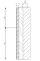
- FIG. 1 the epitaxial layer 2 is formed on the high resistance substrate 1 by, for example, MOCVD (Metal-Organic-Chemical-Vapor-Deposition). Then, the buried oxide film 3 and the SOI layer 4 are formed by wafer bonding by the smart cut method, and an SOI substrate is manufactured (FIG. 2A).
- MOCVD Metal-Organic-Chemical-Vapor-Deposition
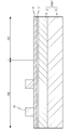
- a photoresist 31 is formed by photolithography.
- the photoresist 31 has an opening in the switch circuit region 102. Further, the photoresist 31 is not formed in the logic circuit region 101 (FIG. 2B).
- dry etching is performed using the photoresist 31 as a mask, and the buried oxide film 3 and the SOI layer 4 are removed. After the etching is completed, the photoresist 31 is removed. At this time, the width of the remaining buried oxide film 3 and SOI layer 4 is 0.6 ⁇ m or less (FIG. 2C).
- an oxide film 21 and a nitride film 22 used as a mask in a later process are formed in the logic circuit area 101 and the switch circuit area 102.
- silicon oxide can be used for the oxide film 21
- silicon nitride can be used for the nitride film 22.
- Each of the oxide film 21 and the nitride film 22 can be formed by, for example, a plasma CVD method (FIG. 2D).
- the photoresist 32 is formed by photolithography.
- the photoresist 32 is formed above the buried oxide film 3 and the SOI layer 4 remaining in the switch circuit region 102.
- an opening is formed in a portion of the logic circuit region 101 where element isolation is provided.
- nitride film dry etching and oxide film dry etching are performed using the photoresist 32 as a mask, and the buried oxide film 3 and the SOI layer 4 in the opening of the photoresist 32 are removed.
- silicon dry etching is performed to form a trench 5 a in the epitaxial layer 2. At this time, etching is performed so that the trench 5a does not penetrate the epitaxial layer 2 (FIG. 2E).
- the photoresist 32 is removed. After removing the photoresist 32, a photoresist 33 is formed by photolithography. The photoresist 33 is formed so as to cover the logic circuit region 101. Note that the photoresist 33 is not formed in the switch circuit region 102. Then, silicon dry etching is performed using the photoresist 33 and the nitride film 22 as a mask, and the trench 5b in the switch circuit region 102 is formed so as to penetrate the epitaxial layer 2 and reach the high resistance substrate 1 (FIG. 2F).
- the photoresist 33 is removed.
- LOCOS oxidation is performed to form LOCOS oxide films 6a and 6b.
- oxidation spreads from the bottom surface (downward) and the side surface (lateral direction) of the trench. That is, as the oxidation spreads in the lateral direction, the buried oxide film 3 and the epitaxial layer 2 below the SOI layer 4 are all oxidized. As the oxidation spreads downward, the high resistance substrate 1 is oxidized toward the bottom surface. As a result, the thickness from the bottom surface of the LOCOS oxide film 6b to the buried oxide film 3 becomes a sufficient thickness of 2.0 ⁇ m or more.
- LOCOS oxidation When LOCOS oxidation is performed, volume expansion occurs as compared to before oxidation, and therefore the buried oxide film 3 and the LOCOS oxide film 6b below the SOI layer 4 expand in the lateral direction. Further, in the logic circuit region 101, oxidation of the trench proceeds and a LOCOS oxide film 6a is formed. The LOCOS oxide film 6a is formed so as to rise from the upper surface of the nitride film 22 due to volume expansion (FIG. 2G).
- an oxide film 7 is formed.
- the oxide film is silicon oxide and can be formed using a plasma CVD method (FIG. 2H).
- planarization is performed to remove the oxide film 7 above the nitride film 22.
- the oxide film 7 is planarized by CMP (Chemical Mechanical Polishing) or etch back (FIG. 2I).
- a photoresist 34 is formed by photolithography. The photoresist 34 is formed so as to cover the switch circuit region 102, but is not formed in the logic circuit region 101.
- using the photoresist 34 as a mask for example, wet etching is performed to remove the oxide film 7 remaining in the logic circuit region 101 (FIG. 2J).
- the well layer 8 of the logic circuit region 101 is formed.
- the nitride film 22 is removed by wet etching. At this time, a slight nitride film 22 remains on the side surfaces of the buried oxide film 3 and the SOI layer 4 via the oxide film 21, but will be omitted hereinafter for the sake of simplifying the drawing.
- a photoresist 35 is formed by photolithography. The photoresist 35 covers the switch circuit region 102, and an opening is formed in a region where the well layer 8 is formed in the logic circuit region 101.
- the well layer 8 is formed in a region sandwiched between the LOCOS oxide films 6a functioning as element isolation, the opening is formed in a region sandwiched between the LOCOS oxide films 6a. Then, ion implantation is performed using the photoresist 35 as a mask to form the well layer 8 (FIG. 2K).
- the photoresist 35 is removed. Then, the oxide film 21 and the portion of the LOCOS oxide film 6a protruding on the epitaxial layer 2 are removed by wet etching, for example. At this time, a slight oxide film 21 remains on the side surfaces of the buried oxide film 3 and the SOI layer 4, but will be omitted hereinafter for the sake of simplifying the drawing. Thereafter, gate oxidation is performed to form a gate oxide film 9a on the logic circuit region 101 and a gate oxide film 9b on the SOI layer 4 (FIG. 2L).
- a gate electrode is formed.
- a polysilicon film 10 that is a material for a gate electrode is formed in the logic circuit region 101 and the switch circuit region 102.
- the polysilicon film 10 can be formed by, for example, an LPCVD (Low Pressure, Chemical, Vapor, Deposition) method (FIG. 2M).
- a photoresist 36 is formed by photolithography.
- the photoresist 36 is formed on the polysilicon film 10 formed in the portion where the gate electrode is formed, that is, the SOI layer 4 and the well layer 8.
- the polysilicon film 10 in the opening of the photoresist 36 is removed by, for example, dry etching.
- the gate electrode 10a of the logic MOSFET 101a is formed in the logic circuit region 101, and the gate electrodes 10b of the switching MOSFETs 102a and 102b are formed in the switch circuit region 102 (FIG. 2N).
- LDD Lightly10Doped Drain
- LDD ion implantation is performed using the gate electrodes 10a and 10b as a mask.
- an oxide film is formed by, for example, plasma CVD, and the formed oxide film is etched back by, for example, dry etching.
- the sidewalls 11 are formed on the side surfaces of the gate electrodes 10a and 10b.
- ion implantation is performed to form a source and a drain (FIG. 2O).
- a source region and a drain region formed by LDD ion implantation and subsequent ion implantation are indicated as a diffusion layer 12a in the logic circuit region 101 and a diffusion layer 12b in the switch circuit region 102. is doing.
- silicides 13a to 13d are formed on the surfaces of the gate electrode and the diffusion layer by, eg, sputtering.
- Silicide 13a is formed on gate electrode 10a
- silicide 13b is formed on diffusion layer 12a.
- Silicide 13c is formed on gate electrode 10b
- silicide 13d is formed on diffusion layer 12b (FIG. 2P).
- the interlayer insulating film 14 is formed by an existing interlayer insulating film forming technique, and the semiconductor device 100 shown in FIG. 1 can be formed.
- the LOCOS oxide film 6b of the switching MOSFETs 102a and 102b is formed using the trench formed in the substrate Sub1 (epitaxial layer 2 and high resistance substrate 1). Therefore, even if the LOCOS oxide film 6b having a thickness of 2.0 ⁇ m or more is formed, the LOCOS oxide film 6b does not protrude above the upper surface of the substrate Sub1 (upper surface of the epitaxial layer 2). Thereby, it is possible to prevent the occurrence of a step due to the formation of the LOCOS oxide film.
- the other steps generated in the manufacturing process are the same in the normal semiconductor process. Therefore, according to the present configuration and the present manufacturing method, it is possible to prevent the occurrence of a high step after the LOCOS oxide film is formed, and to provide a semiconductor device having a high dimensional accuracy and a good yield.
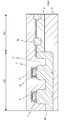
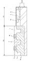
- FIG. 3 is a sectional view schematically showing the configuration of the semiconductor device 200 according to the second embodiment.
- the semiconductor device 200 includes the interface carrier suppression layer 15 below the LOCOS oxide film 6b. That is, the substrate Sub2 of the semiconductor device 200 has a configuration in which the interface carrier suppression layer 15 is added to the substrate Sub1 of the semiconductor device 200.
- the interface carrier suppression layer 15 is configured as a layer having a resistivity lower than that of the high resistance substrate 1. Since other configurations of the semiconductor device 200 are the same as those of the semiconductor device 100, description thereof is omitted.
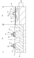
- FIG. 2A showing the manufacturing method of the semiconductor device 100 is replaced with FIG. 4A and FIG. 4B.
- a photoresist 37 is formed on the epitaxial layer 2 by photolithography so as to cover only the logic circuit region 101 (FIG. 4A). Then, the interface carrier suppression layer 15 is formed in a predetermined depth region of the high resistance substrate 1 by high energy ion implantation (FIG. 4B). Since the manufacturing process after removing the photoresist 37 is the same as that in FIGS. 2B to 2P except that the interface carrier suppression layer 15 is present, the description thereof is omitted.
- a depletion layer may be formed in a high-resistance substrate in a lower region of a thick oxide film such as the LOCOS oxide film 6b.
- a situation in which high-speed operation of the semiconductor device is hindered may occur.
- the interface carrier suppression layer 15 is formed below the LOCOS oxide film 6b. This can prevent a depletion layer in the high resistance substrate in the lower region of the LOCOS oxide film 6b. Therefore, according to the present configuration and the present manufacturing method, it is possible to provide not only the same effects as the semiconductor device 100 and the manufacturing method thereof, but also the semiconductor device excellent in high-speed operation and the manufacturing method thereof.
- the trench 5b may be formed without penetrating the epitaxial layer 2. Moreover, the trench 5b may penetrate the interface carrier suppression layer 15 or may not penetrate.
- oxide film and a nitride film are merely examples, and other insulating films such as silicon oxide, silicon nitride, and silicon oxynitride can be applied.
- semiconductor (silicon) conductivity type is merely an example, and for example, p-type and n-type may be interchanged.
Landscapes
- Metal-Oxide And Bipolar Metal-Oxide Semiconductor Integrated Circuits (AREA)
- Element Separation (AREA)
- Thin Film Transistor (AREA)
Abstract
Description
本発明の実施の形態1にかかる半導体装置100について説明する。図1は、実施の形態1にかかる半導体装置100の構成を模式的に示す断面図である。半導体装置100は、高抵抗基板1上にモノリシック集積されたロジック回路領域101及びスイッチ回路領域102を有する。ロジック回路領域101には、例えば図1のように、ロジック用MOSFET101aが形成される。スイッチ回路領域102には、スイッチ用MOSFET102a及び102bが形成される。
次に、本発明の実施の形態2にかかる半導体装置200について説明する。図3は、実施の形態2にかかる半導体装置200の構成を模式的に示す断面図である。半導体装置200は、LOCOS酸化膜6bの下部に、界面キャリア抑制層15を有する。すなわち、半導体装置200の基板Sub2は、半導体装置200の基板Sub1に界面キャリア抑制層15を追加した構成を有する。界面キャリア抑制層15は、高抵抗基板1よりも抵抗率が小さい層として構成される。半導体装置200のその他の構成は、半導体装置100と同様であるので説明を省略する。
2 エピタキシャル層
3 埋め込み酸化膜
4 SOI層
5 トレンチ
6a、6b LOCOS酸化膜
7 酸化膜
8 ウェル層
9a、9b ゲート酸化膜
10 ポリシリコン膜
10a、10b ゲート電極
11 サイドウォール
12a、12b 拡散層
13a~13d シリサイド
14 層間絶縁膜
15 界面キャリア抑制層
21 酸化膜
22 窒化膜
31~37 フォトレジスト
100、200、300 半導体装置
101 ロジック回路領域
102 スイッチ回路領域
101a ロジック用MOSFET
102a、102b スイッチ用MOSFET
310 第1の領域
312 第2の領域
313 高耐圧トランジスタ
314 シリコン基板
315 電界効果トランジスタ
316 ウェル
318 埋め込み酸化膜
320、326、328 素子分離用LOCOS酸化膜
322、324 オフセット用LOCOS酸化膜
330、332 チャネルストッパ領域
334a、336a、354、356 ソース/ドレイン
334b、336b ソース/ドレインのオフセット
338、358 ゲート酸化膜
340、360 ゲート電極
342、344、362、364 スルーホール
346、348、366、368 アルミ配線
350 層間絶縁膜
352 ボディ領域
Sub1、Sub2 基板
Claims (15)
- 高抵抗基板上に形成された第1のMOSFETと、
前記高抵抗基板上に前記第1のMOSFETとモノリシック集積された第2のMOSFETと、を備え、
前記第1のMOSFETは、
前記高抵抗基板上に形成された第1の半導体層と、
前記第1の半導体層の上部に形成された、当該第1のMOSFETのウェル層である第2の半導体層と、を備え、
前記第2のMOSFETは、
前記高抵抗基板上に形成され、2つのトレンチで挟まれることにより上部がメサ形状を有し、前記メサ形状の上面が前記第1の半導体層と同じ高さである第1の絶縁層と、
前記第1の絶縁層の前記メサ形状の上に形成された第2の絶縁層と、
前記第2の絶縁層上に形成された、当該第2のMOSFETのウェル層である第3の半導体層と、を備える、
半導体装置。 - 前記第1のMOSFETは、
前記第1の半導体層の上部に前記第2の半導体層を挟んで形成された第1及び第2の素子分離と、
前記第2の半導体層の上部に離間して形成された第1及び第2の拡散層と、
前記第1及び第2の拡散層間の前記第2の半導体層上に形成された第1のゲート絶縁膜と、
前記第1のゲート絶縁膜上に形成された第1のゲート電極と、を更に備え、
前記第2のMOSFETは、
前記第3の半導体層の上部に離間して形成された第3及び第4の拡散層と、
前記第3及び第4の拡散層間の前記第3の半導体層上に形成された第2のゲート絶縁膜と、
前記第2のゲート絶縁膜上に形成された第2のゲート電極と、を更に備えることを特徴とする、
請求項1に記載の半導体装置。 - 前記高抵抗基板と前記第1の絶縁層との間に形成された、前記高抵抗基板よりも抵抗率が小さい第4の半導体層を備えることを特徴とする、
請求項1又は2に記載の半導体装置。 - 高抵抗基板上に形成された第1のMOSFETと、
前記高抵抗基板上に前記第1のMOSFETとモノリシック集積された第2のMOSFETと、を備え、
前記第1のMOSFETは、
前記高抵抗基板上に形成された第1の半導体層と、
前記第1の半導体層の上部に形成された、当該第1のMOSFETのウェル層である第2の半導体層と、を備え、
前記第2のMOSFETは、
前記高抵抗基板上に形成された前記第1の半導体層にトレンチが形成され、その後当該トレンチの側面及び底面から酸化処理されることにより上部が2つのトレンチに挟まれたメサ形状を有する第1の絶縁層と、
前記第1の絶縁層の前記メサ形状の上に形成された第2の絶縁層と、
前記第2の絶縁層上に形成された、当該第2のMOSFETのウェル層である第3の半導体層と、を備える、
半導体装置。 - 前記第1のMOSFETは、
前記第1の半導体層の上部に前記第2の半導体層を挟んで形成された第1及び第2の素子分離と、
前記第2の半導体層の上部に離間して形成された第1及び第2の拡散層と、
前記第1及び第2の拡散層間の前記第2の半導体層上に形成された第1のゲート絶縁膜と、
前記第1のゲート絶縁膜上に形成された第1のゲート電極と、を更に備え、
前記第2のMOSFETは、
前記第3の半導体層の上部に離間して形成された第3及び第4の拡散層と、
前記第3及び第4の拡散層間の前記第3の半導体層上に形成された第2のゲート絶縁膜と、
前記第2のゲート絶縁膜上に形成された第2のゲート電極と、を更に備えることを特徴とする、
請求項4に記載の半導体装置。 - 前記高抵抗基板と前記第1の絶縁層との間に形成された、前記高抵抗基板よりも抵抗率が小さい第4の半導体層を備えることを特徴とする、
請求項4又は5に記載の半導体装置。 - 前記第2のMOSFETの前記高抵抗基板上に形成された前記第1の半導体層に、当該第1の半導体層を貫通しないトレンチが形成されることを特徴とする、
請求項4乃至6のいずれか一項に記載の半導体装置。 - 前記第2のMOSFETの前記高抵抗基板上に形成された前記第1の半導体層に、前記高抵抗基板に達するトレンチが形成されることを特徴とする、
請求項4乃至6のいずれか一項に記載の半導体装置。 - 前記第2のMOSFETの前記高抵抗基板上に形成された前記第1の半導体層に、当該第1の半導体層を貫通して前記第4の半導体層に達するトレンチが形成されることを特徴とする、
請求項6に記載の半導体装置。 - 前記高抵抗基板上に第1の半導体層を形成し、
前記第1の半導体層上に第2の絶縁層を形成し、
前記第2の絶縁層上に、第2のMOSFETのウェル層となる第3の半導体層を形成し、
第1の領域の前記第2の絶縁層及び前記第3の半導体層を除去するとともに、第2の領域の前記第2の絶縁層及び第3の半導体層に開口部を形成し、
前記第2の領域の前記第2の絶縁層及び前記第3の半導体層に形成された前記開口部の前記第1の半導体層をエッチングしてトレンチを形成することにより、2つの前記トレンチに挟まれたメサ形状を前記第2の絶縁層及び前記第3の半導体層下方の前記第1の半導体層に形成し、
前記トレンチの側面及び底面から酸化処理を行うことにより、2つのトレンチで挟まれることにより上部がメサ形状を有する第1の絶縁層を形成し、
前記第1の領域の前記第1の半導体層の上部に、第1のMOSFETのウェル層となる第2の半導体層を形成する、
半導体装置の製造方法。 - 前記第2の半導体層の形成に先立ち、前記第1の領域の前記第1の半導体層の上部に第1及び第2の素子分離を離間して形成し、
前記第1及び第2の素子分離の間の前記第1の半導体層にイオン注入を行うことにより、前記第2の半導体層を形成し、
前記第2の半導体層上に第1のゲート絶縁膜を形成するとともに、前記第3の半導体層上に第2のゲート絶縁膜を形成し、
前記第1のゲート絶縁膜上に第1のゲート電極を形成するとともに、前記第2のゲート絶縁膜上に第2のゲート電極を形成し、
前記第1のゲート電極をマスクとして前記第1のゲート絶縁膜をエッチングするとともに、前記第2のゲート電極をマスクとして前記第2のゲート絶縁膜をエッチングし、
前記第1のゲート電極をマスクとして前記第2の半導体層にイオン注入を行うことにより第1及び第2の拡散層を形成するとともに、前記第2のゲート電極をマスクとして前記第3の半導体層にイオン注入を行うことにより第3及び第4の拡散層を形成することを特徴とする、
請求項10に記載の半導体装置の製造方法。 - 前記第1の半導体層を形成した後に、イオン注入により前記高抵抗基板と前記第1の半導体層との間に、前記高抵抗基板よりも抵抗率が小さい第4の半導体層を形成することを特徴とする、
請求項10又は11に記載の半導体装置の製造方法。 - 前記第2の領域の前記第1の半導体層に形成するトレンチを、前記第1の半導体層を貫通せずに形成することを特徴とする、
請求項10乃至12のいずれか一項に記載の半導体装置の製造方法。 - 前記第1の領域の前記第1の半導体層に形成するトレンチを、前記高抵抗基板に達するように形成することを特徴とする、
請求項10乃至12のいずれか一項に記載の半導体装置の製造方法。 - 前記第1の領域の前記第1の半導体層に形成するトレンチを、前記第1の半導体層を貫通して前記第4の半導体層に達するように形成することを特徴とする、
請求項12に記載の半導体装置の製造方法。
Priority Applications (3)
| Application Number | Priority Date | Filing Date | Title |
|---|---|---|---|
| US14/007,760 US9064742B2 (en) | 2011-03-29 | 2012-02-24 | Semiconductor device and manufacturing method thereof |
| JP2013507105A JP5635680B2 (ja) | 2011-03-29 | 2012-02-24 | 半導体装置及びその製造方法 |
| US14/715,945 US20150249128A1 (en) | 2011-03-29 | 2015-05-19 | Semiconductor device and manufacturing method thereof |
Applications Claiming Priority (2)
| Application Number | Priority Date | Filing Date | Title |
|---|---|---|---|
| JP2011072699 | 2011-03-29 | ||
| JP2011-072699 | 2011-03-29 |
Related Child Applications (2)
| Application Number | Title | Priority Date | Filing Date |
|---|---|---|---|
| US14/007,760 A-371-Of-International US9064742B2 (en) | 2011-03-29 | 2012-02-24 | Semiconductor device and manufacturing method thereof |
| US14/715,945 Continuation US20150249128A1 (en) | 2011-03-29 | 2015-05-19 | Semiconductor device and manufacturing method thereof |
Publications (1)
| Publication Number | Publication Date |
|---|---|
| WO2012132219A1 true WO2012132219A1 (ja) | 2012-10-04 |
Family
ID=46930015
Family Applications (1)
| Application Number | Title | Priority Date | Filing Date |
|---|---|---|---|
| PCT/JP2012/001285 Ceased WO2012132219A1 (ja) | 2011-03-29 | 2012-02-24 | 半導体装置及びその製造方法 |
Country Status (3)
| Country | Link |
|---|---|
| US (2) | US9064742B2 (ja) |
| JP (1) | JP5635680B2 (ja) |
| WO (1) | WO2012132219A1 (ja) |
Cited By (3)
| Publication number | Priority date | Publication date | Assignee | Title |
|---|---|---|---|---|
| EP2757581A1 (en) * | 2013-01-22 | 2014-07-23 | Nxp B.V. | Semiconductor device |
| US9570437B2 (en) | 2014-01-09 | 2017-02-14 | Nxp B.V. | Semiconductor die, integrated circuits and driver circuits, and methods of maufacturing the same |
| JPWO2018159126A1 (ja) * | 2017-03-03 | 2019-12-26 | ソニーセミコンダクタソリューションズ株式会社 | 半導体装置および半導体装置の製造方法並びに電子機器 |
Families Citing this family (5)
| Publication number | Priority date | Publication date | Assignee | Title |
|---|---|---|---|---|
| US9281305B1 (en) * | 2014-12-05 | 2016-03-08 | National Applied Research Laboratories | Transistor device structure |
| DE102016124207B4 (de) * | 2016-12-13 | 2023-04-27 | Infineon Technologies Ag | Verfahren zur bildung vergrabener isolierungsgebiete |
| US10263013B2 (en) * | 2017-02-24 | 2019-04-16 | Globalfoundries Inc. | Method of forming an integrated circuit (IC) with hallow trench isolation (STI) regions and the resulting IC structure |
| US10340290B2 (en) * | 2017-09-15 | 2019-07-02 | Globalfoundries Inc. | Stacked SOI semiconductor devices with back bias mechanism |
| TWI776911B (zh) | 2018-07-02 | 2022-09-11 | 聯華電子股份有限公司 | 半導體元件及其製作方法 |
Citations (5)
| Publication number | Priority date | Publication date | Assignee | Title |
|---|---|---|---|---|
| JPH07153837A (ja) * | 1993-11-30 | 1995-06-16 | Sony Corp | 半導体装置及び半導体装置の製造方法 |
| JP2001007196A (ja) * | 1999-06-18 | 2001-01-12 | Sharp Corp | 半導体装置の製造方法 |
| JP2001007219A (ja) * | 1999-06-21 | 2001-01-12 | Seiko Epson Corp | 半導体装置及びその製造方法 |
| JP2004214596A (ja) * | 2002-11-12 | 2004-07-29 | Denso Corp | 半導体基板およびその製造方法 |
| JP2008172082A (ja) * | 2007-01-12 | 2008-07-24 | Toshiba Corp | 半導体装置及び半導体装置の製造方法 |
Family Cites Families (10)
| Publication number | Priority date | Publication date | Assignee | Title |
|---|---|---|---|---|
| JPH08102498A (ja) | 1994-09-30 | 1996-04-16 | Hitachi Ltd | 半導体装置 |
| JPH08222710A (ja) * | 1995-02-17 | 1996-08-30 | Mitsubishi Electric Corp | 半導体装置 |
| TW473932B (en) * | 2000-04-18 | 2002-01-21 | Taiwan Semiconductor Mfg | CMOS transistor on thin silicon-on-insulator using accumulation as conduction mechanism |
| JP4322453B2 (ja) * | 2001-09-27 | 2009-09-02 | 株式会社東芝 | 半導体装置およびその製造方法 |
| US7129142B2 (en) * | 2002-06-11 | 2006-10-31 | Advanced Micro Devices, Inc. | Method of forming doped regions in the bulk substrate of an SOI substrate to control the operational characteristics of transistors formed thereabove, and an integrated circuit device comprising same |
| US20050045992A1 (en) * | 2003-08-27 | 2005-03-03 | Turley Alfred P. | Bipolar/thin film SOI CMOS structure and method of making same |
| US20070069300A1 (en) * | 2005-09-29 | 2007-03-29 | International Business Machines Corporation | Planar ultra-thin semiconductor-on-insulator channel mosfet with embedded source/drain |
| JP5005224B2 (ja) | 2006-01-27 | 2012-08-22 | ルネサスエレクトロニクス株式会社 | 半導体装置及びその製造方法 |
| JP5057804B2 (ja) | 2007-03-12 | 2012-10-24 | 株式会社東芝 | 半導体装置 |
| JP5528667B2 (ja) * | 2007-11-28 | 2014-06-25 | ルネサスエレクトロニクス株式会社 | 半導体装置および半導体装置の制御方法 |
-
2012
- 2012-02-24 JP JP2013507105A patent/JP5635680B2/ja not_active Expired - Fee Related
- 2012-02-24 US US14/007,760 patent/US9064742B2/en active Active
- 2012-02-24 WO PCT/JP2012/001285 patent/WO2012132219A1/ja not_active Ceased
-
2015
- 2015-05-19 US US14/715,945 patent/US20150249128A1/en not_active Abandoned
Patent Citations (5)
| Publication number | Priority date | Publication date | Assignee | Title |
|---|---|---|---|---|
| JPH07153837A (ja) * | 1993-11-30 | 1995-06-16 | Sony Corp | 半導体装置及び半導体装置の製造方法 |
| JP2001007196A (ja) * | 1999-06-18 | 2001-01-12 | Sharp Corp | 半導体装置の製造方法 |
| JP2001007219A (ja) * | 1999-06-21 | 2001-01-12 | Seiko Epson Corp | 半導体装置及びその製造方法 |
| JP2004214596A (ja) * | 2002-11-12 | 2004-07-29 | Denso Corp | 半導体基板およびその製造方法 |
| JP2008172082A (ja) * | 2007-01-12 | 2008-07-24 | Toshiba Corp | 半導体装置及び半導体装置の製造方法 |
Cited By (5)
| Publication number | Priority date | Publication date | Assignee | Title |
|---|---|---|---|---|
| EP2757581A1 (en) * | 2013-01-22 | 2014-07-23 | Nxp B.V. | Semiconductor device |
| EP2757580A1 (en) * | 2013-01-22 | 2014-07-23 | Nxp B.V. | Bipolar cmos dmos (bcd) processes |
| US9570437B2 (en) | 2014-01-09 | 2017-02-14 | Nxp B.V. | Semiconductor die, integrated circuits and driver circuits, and methods of maufacturing the same |
| JPWO2018159126A1 (ja) * | 2017-03-03 | 2019-12-26 | ソニーセミコンダクタソリューションズ株式会社 | 半導体装置および半導体装置の製造方法並びに電子機器 |
| JP7039552B2 (ja) | 2017-03-03 | 2022-03-22 | ソニーセミコンダクタソリューションズ株式会社 | 半導体装置および半導体装置の製造方法並びに電子機器 |
Also Published As
| Publication number | Publication date |
|---|---|
| JP5635680B2 (ja) | 2014-12-03 |
| US9064742B2 (en) | 2015-06-23 |
| JPWO2012132219A1 (ja) | 2014-07-24 |
| US20140015050A1 (en) | 2014-01-16 |
| US20150249128A1 (en) | 2015-09-03 |
Similar Documents
| Publication | Publication Date | Title |
|---|---|---|
| JP5635680B2 (ja) | 半導体装置及びその製造方法 | |
| US10050122B2 (en) | Semiconductor device and manufacturing method of the same | |
| JP5695730B2 (ja) | 薄いbox金属バックゲート型極薄soiデバイス | |
| US7732839B2 (en) | Semiconductor device and method for fabricating the same | |
| US8716800B2 (en) | Semiconductor structure and method for manufacturing the same | |
| US9159807B2 (en) | Semiconductor device and manufacturing method thereof | |
| US9130060B2 (en) | Integrated circuit having a vertical power MOS transistor | |
| US9899417B2 (en) | Semiconductor structure including a first transistor and a second transistor | |
| JP5968708B2 (ja) | 半導体装置 | |
| JP2010010215A (ja) | 半導体装置の製造方法 | |
| JP2009302317A (ja) | 半導体装置およびその製造方法 | |
| US20190051565A1 (en) | Cmos devices and manufacturing method thereof | |
| US10211336B2 (en) | LDMOS transistor structures and integrated circuits including LDMOS transistor structures | |
| KR20070080583A (ko) | 반도체 장치 및 그 제조 방법 | |
| US9178070B2 (en) | Semiconductor structure and method for manufacturing the same | |
| CN104143555A (zh) | 具有硅局部氧化的绝缘体上硅的集成电路及其制造方法 | |
| US8637938B2 (en) | Semiconductor device with pocket regions and method of manufacturing the same | |
| KR20190128374A (ko) | 반도체 장치 및 그 제조 방법 | |
| EP3154093A1 (en) | Transistor and method for forming the same | |
| JP6574885B2 (ja) | 半導体装置の製造方法 | |
| CN107316870A (zh) | 使用绝缘体上硅类型技术的特别用于高压的 mos 晶体管结构 | |
| KR20210107081A (ko) | 디지털 및 무선 주파수 어플리케이션을 위한 반도체 구조체 | |
| JP5092313B2 (ja) | 半導体装置の製造方法 | |
| KR100827531B1 (ko) | 반도체 소자 및 그 제조 방법 | |
| JP2005276913A (ja) | 半導体装置および半導体装置の製造方法 |
Legal Events
| Date | Code | Title | Description |
|---|---|---|---|
| 121 | Ep: the epo has been informed by wipo that ep was designated in this application |
Ref document number: 12764881 Country of ref document: EP Kind code of ref document: A1 |
|
| ENP | Entry into the national phase |
Ref document number: 2013507105 Country of ref document: JP Kind code of ref document: A |
|
| WWE | Wipo information: entry into national phase |
Ref document number: 14007760 Country of ref document: US |
|
| NENP | Non-entry into the national phase |
Ref country code: DE |
|
| 122 | Ep: pct application non-entry in european phase |
Ref document number: 12764881 Country of ref document: EP Kind code of ref document: A1 |