WO2012120785A1 - シリコンウェーハの製造方法 - Google Patents
シリコンウェーハの製造方法 Download PDFInfo
- Publication number
- WO2012120785A1 WO2012120785A1 PCT/JP2012/000856 JP2012000856W WO2012120785A1 WO 2012120785 A1 WO2012120785 A1 WO 2012120785A1 JP 2012000856 W JP2012000856 W JP 2012000856W WO 2012120785 A1 WO2012120785 A1 WO 2012120785A1
- Authority
- WO
- WIPO (PCT)
- Prior art keywords
- polishing
- oxide film
- silicon wafer
- wafer
- polished
- Prior art date
- Legal status (The legal status is an assumption and is not a legal conclusion. Google has not performed a legal analysis and makes no representation as to the accuracy of the status listed.)
- Ceased
Links
Images



Classifications
-
- H—ELECTRICITY
- H10—SEMICONDUCTOR DEVICES; ELECTRIC SOLID-STATE DEVICES NOT OTHERWISE PROVIDED FOR
- H10P—GENERIC PROCESSES OR APPARATUS FOR THE MANUFACTURE OR TREATMENT OF DEVICES COVERED BY CLASS H10
- H10P14/00—Formation of materials, e.g. in the shape of layers or pillars
- H10P14/60—Formation of materials, e.g. in the shape of layers or pillars of insulating materials
- H10P14/63—Formation of materials, e.g. in the shape of layers or pillars of insulating materials characterised by the formation processes
- H10P14/6302—Non-deposition formation processes
- H10P14/6304—Formation by oxidation, e.g. oxidation of the substrate
- H10P14/6306—Formation by oxidation, e.g. oxidation of the substrate of the semiconductor materials
- H10P14/6308—Formation by oxidation, e.g. oxidation of the substrate of the semiconductor materials of Group IV semiconductors
-
- B—PERFORMING OPERATIONS; TRANSPORTING
- B24—GRINDING; POLISHING
- B24B—MACHINES, DEVICES, OR PROCESSES FOR GRINDING OR POLISHING; DRESSING OR CONDITIONING OF ABRADING SURFACES; FEEDING OF GRINDING, POLISHING, OR LAPPING AGENTS
- B24B37/00—Lapping machines or devices; Accessories
- B24B37/04—Lapping machines or devices; Accessories designed for working plane surfaces
- B24B37/07—Lapping machines or devices; Accessories designed for working plane surfaces characterised by the movement of the work or lapping tool
- B24B37/08—Lapping machines or devices; Accessories designed for working plane surfaces characterised by the movement of the work or lapping tool for double side lapping
-
- B—PERFORMING OPERATIONS; TRANSPORTING
- B24—GRINDING; POLISHING
- B24B—MACHINES, DEVICES, OR PROCESSES FOR GRINDING OR POLISHING; DRESSING OR CONDITIONING OF ABRADING SURFACES; FEEDING OF GRINDING, POLISHING, OR LAPPING AGENTS
- B24B37/00—Lapping machines or devices; Accessories
- B24B37/11—Lapping tools
- B24B37/20—Lapping pads for working plane surfaces
- B24B37/24—Lapping pads for working plane surfaces characterised by the composition or properties of the pad materials
-
- H—ELECTRICITY
- H10—SEMICONDUCTOR DEVICES; ELECTRIC SOLID-STATE DEVICES NOT OTHERWISE PROVIDED FOR
- H10P—GENERIC PROCESSES OR APPARATUS FOR THE MANUFACTURE OR TREATMENT OF DEVICES COVERED BY CLASS H10
- H10P14/00—Formation of materials, e.g. in the shape of layers or pillars
- H10P14/20—Formation of materials, e.g. in the shape of layers or pillars of semiconductor materials
- H10P14/34—Deposited materials, e.g. layers
- H10P14/3402—Deposited materials, e.g. layers characterised by the chemical composition
- H10P14/3404—Deposited materials, e.g. layers characterised by the chemical composition being Group IVA materials
- H10P14/3411—Silicon, silicon germanium or germanium
-
- H—ELECTRICITY
- H10—SEMICONDUCTOR DEVICES; ELECTRIC SOLID-STATE DEVICES NOT OTHERWISE PROVIDED FOR
- H10P—GENERIC PROCESSES OR APPARATUS FOR THE MANUFACTURE OR TREATMENT OF DEVICES COVERED BY CLASS H10
- H10P14/00—Formation of materials, e.g. in the shape of layers or pillars
- H10P14/60—Formation of materials, e.g. in the shape of layers or pillars of insulating materials
- H10P14/69—Inorganic materials
- H10P14/6903—Inorganic materials containing silicon
-
- H—ELECTRICITY
- H10—SEMICONDUCTOR DEVICES; ELECTRIC SOLID-STATE DEVICES NOT OTHERWISE PROVIDED FOR
- H10P—GENERIC PROCESSES OR APPARATUS FOR THE MANUFACTURE OR TREATMENT OF DEVICES COVERED BY CLASS H10
- H10P52/00—Grinding, lapping or polishing of wafers, substrates or parts of devices
-
- H—ELECTRICITY
- H10—SEMICONDUCTOR DEVICES; ELECTRIC SOLID-STATE DEVICES NOT OTHERWISE PROVIDED FOR
- H10P—GENERIC PROCESSES OR APPARATUS FOR THE MANUFACTURE OR TREATMENT OF DEVICES COVERED BY CLASS H10
- H10P52/00—Grinding, lapping or polishing of wafers, substrates or parts of devices
- H10P52/40—Chemomechanical polishing [CMP]
- H10P52/402—Chemomechanical polishing [CMP] of semiconductor materials
-
- H—ELECTRICITY
- H10—SEMICONDUCTOR DEVICES; ELECTRIC SOLID-STATE DEVICES NOT OTHERWISE PROVIDED FOR
- H10P—GENERIC PROCESSES OR APPARATUS FOR THE MANUFACTURE OR TREATMENT OF DEVICES COVERED BY CLASS H10
- H10P90/00—Preparation of wafers not covered by a single main group of this subclass, e.g. wafer reinforcement
- H10P90/12—Preparing bulk and homogeneous wafers
- H10P90/129—Preparing bulk and homogeneous wafers by polishing
Definitions
- the present invention relates to a method for producing a silicon wafer for producing an epitaxial silicon wafer, having a mirror-polished surface on one side and a protective film for preventing dopant volatilization on the other surface.
- Semiconductor epitaxial wafers have been widely used due to their excellent characteristics as wafers for manufacturing discrete semiconductors, bipolar ICs, and the like. Semiconductor epitaxial wafers are also widely used in microprocessor units and flash memory devices because MOS errors have excellent soft errors and latch-up characteristics.
- Such a semiconductor epitaxial wafer is manufactured as follows, for example.
- a single crystal ingot is generally manufactured by a Czochralski (CZ) method or a floating zone (FZ) method.
- the manufactured single crystal ingot is cut into blocks and subjected to a rounding process (cylindrical grinding process) in order to make the diameters uniform.
- a plurality of wafers are cut out from the single crystal ingot block (slicing process), and chamfering (beveling process) is performed to drop the corners of the peripheral portion of the cut wafer.
- mechanical grinding lapping process
- the processing strain layer formed on the surface layer of the wafer during mechanical grinding is removed by mixed acid etching or the like (etching process).
- a protective film (protective film for preventing dopant volatilization) for preventing autodoping is formed at least on the back side of the wafer, and then the surface of the semiconductor wafer is polished by chemical and mechanical polishing (CMP).
- CMP chemical and mechanical polishing
- Mirror polishing mirror polishing process
- a semiconductor epitaxial wafer is manufactured through a process of forming an epitaxial film on the surface of the mirror-polished wafer.
- autodoping In an epitaxial process in which a single crystal thin film (epitaxial film) is vapor-grown on a wafer, the wafer is usually exposed to a high temperature of about 1000 to 1200 ° C. At that time, the dopant contained in the wafer is volatilized during the process of forming the epitaxial film and is taken into the epitaxial film, so-called auto-doping phenomenon occurs.
- a low resistivity wafer of either P-type or N-type conductivity doped with impurities at a high concentration is used as a substrate for epitaxial film formation. In this case, the occurrence of auto doping becomes significant.
- a dopant volatilization prevention protective film is required on the back surface of the wafer in order to prevent autodoping.
- a chemical vapor deposition method using an oxide film as a protective film for preventing dopant volatilization after performing double-side polishing and highly planarizing the wafer is formed on the back side of the wafer by (CVD) or the like.
- the surface side of the silicon wafer that is, the side on which the epitaxial film is vapor-phase grown is mirror-polished by single-side polishing, but distortion or the like is caused on the silicon surface by the oxide film forming step by CVD.
- this single-side polishing it is necessary to polish the silicon surface side by several microns or more to finish it as a mirror surface.
- Patent Document 1 discloses a semiconductor wafer that has a mirror surface and a rough surface by polishing a wafer having an oxide film grown on one side by CVD using a double-side polishing apparatus, and enables processing of a wafer with high flatness. A manufacturing method is disclosed.
- this method is intended to produce a highly flat wafer having one rough surface, and the oxide film is removed by double-side polishing.
- the thickness of the oxide film and the polishing allowance at the time of double-side polishing are adjusted by using this method so that the oxide film remains, the oxide film is thinned by polishing or the oxide film surface is damaged. Therefore, there arises a problem that quality as a protective film for preventing dopant volatilization cannot be obtained.
- the present invention has been made in view of the above-mentioned problems, and manufactures a silicon wafer having high flatness while suppressing the scratches and polishing amount of the oxide film and maintaining the quality as a protective film for preventing dopant volatilization.
- An object of the present invention is to provide a method for manufacturing a silicon wafer.
- the surface of the raw silicon wafer on the side on which the oxide film is not grown Is a manufacturing method for manufacturing a silicon wafer having a mirror polished surface and an oxide film surface, and after the oxide film is grown, wet-coagulated after applying urethane resin on the oxide film surface side
- a velor-based polishing cloth in which a urethane resin is impregnated with a suede-based polishing cloth or a non-woven fabric that has been foamed and a polishing cloth having an Asker C rubber hardness of 50 ° or more and less than 90 °, and the surface on which the oxide film is not grown The raw material is a velor-based polishing cloth in which a urethane single-foam polishing cloth or a nonwoven fabric is impregnated with a urethane resin, and a polishing cloth having an Asker C rubber hardness
- the oxide film is not overpolished, the scratches on the oxide film can be suppressed, and the silicon wafer can be polished to a high flatness, which is oxidized as a protective film for preventing dopant volatilization.
- a silicon wafer having high flatness can be manufactured while maintaining the quality of the film.
- the mirror-polished surface can be polished using a single-side polishing apparatus after the double-side polishing step. In this way, the flatness of the silicon wafer can be further improved, and the mirror-polished surface can be finished with high accuracy.
- a silicon wafer having a resistivity of 0.1 ⁇ ⁇ cm or less can be used as the raw material silicon wafer. Even in the case of using a low resistivity silicon wafer that is prone to autodoping in the epitaxial wafer process in the subsequent process, the present invention suppresses scratches on the oxide film as the protective film for preventing dopant volatilization, A silicon wafer that can reliably prevent autodoping can be manufactured.
- the Asker C rubber hardness of the polishing cloth on the surface of the oxide film is preferably 50 ° or more and 70 ° or less. In this way, in double-side polishing, scratches on the oxide film can be more reliably suppressed and polishing can be performed more reliably and highly flatly.
- an oxide film is grown on one surface of a raw material silicon wafer by chemical vapor deposition, and then urethane is applied to the surface of the oxide film on the surface of the oxide film by applying a urethane resin and then wet-solidifying and foaming.
- an oxide film as a protective film for preventing dopant volatilization is formed on the back side of the wafer in order to prevent autodoping.
- This oxide film is formed by CVD, but the silicon surface is distorted during this CVD.
- the polishing allowance must be several microns or more when the surface on the side on which the epitaxial film is vapor-phase grown is finished to a mirror surface by single-side polishing.
- a semiconductor wafer manufacturing method for manufacturing a wafer having a mirror surface and a rough surface by polishing a wafer having an oxide film grown on one side by CVD with a double-side polishing apparatus and a high flatness is known.
- the oxide film is thinned by polishing or scratches are generated on the surface of the oxide film, so that it does not function as a protective film for preventing dopant volatilization.
- it is difficult to manufacture a wafer having high flatness while maintaining the quality of the oxide film for preventing dopant volatilization.
- the present inventors have conducted intensive studies to solve such problems.
- the mirror polishing of the surface on the vapor phase growth side of the epitaxial film is performed by double-side polishing, and the quality and quality of the oxide film is defined by defining the material and hardness of the upper and lower polishing cloths at this time.
- the inventors have found that a wafer having high flatness can be produced while keeping it, and have completed the present invention.
- FIG. 1 is a flowchart showing an example of a method for producing a silicon wafer according to the present invention.
- a raw material silicon wafer in which an oxide film for preventing dopant volatilization is grown on one side is prepared as follows.
- the process until the oxide film is grown is basically the same as the conventional process.
- the surface of the raw material silicon wafer on which the oxide film is formed is referred to as a back surface, and the surface on which the oxide film is not formed but is mirror-polished to form an epitaxial film may be referred to as the surface.
- a silicon ingot is manufactured by the CZ method or the FZ method.
- the manufactured silicon ingot is cut into blocks having a predetermined length and subjected to a rounding process (cylindrical grinding process) to make the diameters uniform. Then, the wafer is cut out from the silicon ingot (slicing process: FIG. 1A).
- chamfering (beveling process: FIG. 1B) is performed in order to drop the corners of the peripheral portion of the cut out raw material silicon wafer. Furthermore, the surface of the wafer is removed by mechanical grinding (lapping process: FIG. 1 (c)) to eliminate unevenness on the surface of the silicon wafer, improve flatness, and minimize processing distortion during slicing.
- the processed strain layer formed in (1) is removed by mixed acid etching or the like (etching step: FIG. 1 (d)).
- the wafer can be polished on both sides before the oxide film growth step for preventing dopant volatilization described later, for example, after the etching step.
- the polishing cloth used for this double-side polishing is not particularly limited, and the same conventional cloth can be used.
- an oxide film for preventing dopant volatilization to prevent autodoping is grown on the back surface of the raw silicon wafer (dopant volatilization preventing oxide film growth step: FIG. 1 (e)).
- this oxide film for preventing dopant volatilization for example, in the epitaxial film forming process and other heat treatment processes, it is strongly suppressed that the dopant doped at a high concentration on the wafer is volatilized and taken into the epitaxial film. be able to.
- a silicon oxide film can be formed as the oxide film for preventing dopant volatilization.
- a silicon oxide film can be easily formed by deposition by atmospheric pressure CVD, formation of a thermal oxide film by thermal oxidation, or the like, and can be manufactured at low cost. Moreover, you may remove the outer peripheral part of the oxide film for this dopant volatilization prevention by an etching or mechanical processing.
- the raw material silicon wafer having an oxide film grown on the back side is polished on both sides, and the front side is made into a mirror-polished surface (mirror polishing process by double-side polishing: FIG. 1 (f)).
- This double-side polishing is performed using, for example, a double-side polishing apparatus as shown in FIG.
- the double-side polishing apparatus 10 has an upper surface plate 11 and a lower surface plate 12 provided to face each other in the vertical direction. Polishing cloths 21 and 22 are affixed to the facing surfaces of the upper and lower surface plates 11 and 12, respectively.
- the upper and lower surface plates 11 and 12 can be rotated in opposite directions by upper and lower surface plate rotating shafts 13 and 14, respectively.
- the lower surface plate 12 is provided with a sun gear 15 at the center thereof, and an annular internal gear 16 is provided at the periphery thereof.
- a carrier 17 having a holding hole for holding the wafer W is disposed between the upper surface of the polishing cloth 22 attached to the lower surface plate 12 and the lower surface of the polishing cloth 21 attached to the upper surface plate 11. Then, when the carrier 17 rotates and revolves by the action of the sun gear 15 and the internal gear 16, the front and back surfaces of the wafer W held in the holding hole of the carrier 17 slide between the upper and lower polishing cloths 21 and 22. It is designed to be polished.
- the following are used as upper and lower polishing cloths used in the double-side polishing. That is, a suede type polishing cloth or a non-woven cloth impregnated with urethane resin on a side where the oxide film is formed (the oxide film surface side) is wet-coagulated after applying urethane resin, or a velour type polishing cloth in which urethane resin is impregnated, and Asker Using a polishing cloth having a C rubber hardness of 50 ° or more and less than 90 °, more preferably 50 ° or more and 70 ° or less, urethane foam on the side where the surface on which the oxide film is not grown is polished (the surface side where mirror polishing is performed) A velor-based polishing cloth in which a body polishing cloth or a nonwoven fabric is impregnated with a urethane resin, and an polishing cloth having an Asker C rubber hardness of 90 ° or more is used.
- the carrier 17 holding the raw silicon wafer W is rotated and revolved while supplying a polishing agent from a plurality of polishing agent supply ports 18 arranged on the upper surface plate 11, and the upper and lower surface plates 11 and 12 are further rotated.
- the raw material silicon wafer W is polished by applying a load.
- a suede type polishing cloth which has been wet-coagulated after foaming urethane resin on the oxide film surface side or a velor type polishing cloth in which urethane resin is impregnated with urethane resin, and Asker C rubber hardness is 50 ° or more 90 ° If a polishing cloth of less than 0 ° is used, the polishing of the oxide film can be reliably suppressed, and the generation of scratches can be effectively suppressed. That is, the quality of the oxide film as the protective film for preventing dopant volatilization for preventing autodoping in the epitaxial process in the subsequent process can be ensured. Moreover, if the Asker C rubber hardness is 50 ° or more, it is possible to reliably prevent adverse effects on the flatness of the wafer due to the polishing cloth being too soft.
- a velor-based polishing cloth in which a urethane single foam polishing cloth or a nonwoven fabric is impregnated with a urethane resin on the surface side to be mirror-polished, and Asker C rubber hardness is 90.
- a polishing cloth having an angle of ⁇ ° a silicon wafer having a high flatness with a mirror-polished surface can be obtained.
- the upper limit of the hardness of the polishing cloth used on the surface side to be mirror-polished is not particularly limited, and a polishing cloth having a hardness up to about 95 ° is currently available.
- polishing agent to be used is not specifically limited, For example, colloidal silica or fumed silica can be used.
- the mirror-polished surface of the wafer can be further polished using a single-side polishing apparatus.
- the mirror polished surface of the wafer can be finished with high accuracy, and the flatness of the silicon wafer can be further improved.
- the distortion of the silicon surface due to CVD has already been removed by the above-described double-side polishing, it is not necessary to increase the polishing allowance of this single-side polishing, and the flatness is not deteriorated by the single-side polishing.
- a silicon wafer having a resistivity of 0.1 ⁇ ⁇ cm or less can be used as a raw material silicon wafer to be used.
- Auto-doping in the epitaxial process occurs remarkably when using a low resistivity wafer doped with impurities at a high concentration, but in the present invention, even when using such a low resistivity silicon wafer, It is possible to manufacture a silicon wafer having high flatness on which an oxide film for preventing dopant volatilization that can reliably prevent autodoping is formed.
- Example 1-5 A silicon single crystal wafer was manufactured by the silicon wafer manufacturing method of the present invention as shown in FIG. 1, and the occurrence rate of scratches on the oxide film surface was evaluated.
- a silicon single crystal ingot was pulled up by the CZ method and sliced to prepare 600 raw material silicon single crystal wafers having a diameter of 300 mm, a crystal orientation ⁇ 100>, and a conductivity type of P type.
- the edges of these wafers were chamfered, lapped, and etched to remove residual strain due to lapping. Thereafter, both surfaces were mirror-polished in order to achieve higher flatness, and mirror chamfering was performed to reduce particles from the edge portion.
- the raw material silicon single crystal wafer was held with the oxide film surface side down, and double-side polished.
- the polishing cloth a urethane single foam polishing cloth with Asker C rubber hardness of 90 ° is used on the side to be mirror-polished, that is, the side to be polished (upper side) where the oxide film is not grown.
- the double-side polishing conditions are shown below.
- the polishing allowance is a value for the surface of the silicon single crystal on the mirror polishing side, and was set to 4 ⁇ m in order to remove the distortion generated on the surface of the silicon single crystal in the oxide film forming process by CVD. Under the following polishing conditions, it was confirmed in advance that the polishing rate of the silicon single crystal surface was 0.1 ⁇ m / min in any of the examples, and the polishing time was set to 40 minutes.
- Raw material wafer P type, crystal orientation ⁇ 100>, diameter 300 mm
- Upper polishing cloth Urethane single foam
- Lower polishing cloth Suede polishing cloth
- Abrasive Colloidal silica abrasive Abrasive load: 100 g / cm 2 Polishing time: 40 minutes
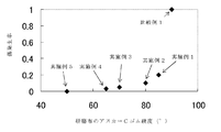
- the mirror-polished surface of the silicon single crystal wafer was further polished with a polishing allowance of 1 ⁇ m using a single-side polishing apparatus. Then, the incidence of scratches on the oxide film of the silicon single crystal wafer was evaluated by inspecting the presence or absence of scratches visually under a fluorescent lamp. The result is shown in FIG.
- the value of the scratch occurrence rate in FIG. 3 shows a numerical value when the scratch occurrence rate of Comparative Example 1 described later is 1.
- FIG. 3 there is a correlation between the hardness of the polishing cloth and the incidence of scratches, and the lower the hardness of the polishing cloth, the fewer the scratches.
- wound is suppressed significantly compared with the result of the comparative example 1, especially when the Asker C rubber hardness is 70 ° or less, the scratch is reduced to 1/10 or less of the comparative example 1.
- the silicon wafer manufacturing method of the present invention can maintain the quality as a protective film for preventing dopant volatilization by suppressing scratches and polishing amount of the oxide film.
- Example 6 300 silicon single crystal wafers under the same conditions as in Example 3 (the Asker C rubber hardness of the lower polishing cloth is 70 °) except that the mirror polishing surface (upper) polishing cloth has an Asker C hardness of 95 °
- the flatness was evaluated.
- SFQR (MAX) was measured using an AFS device manufactured by ADE, and the value was obtained by excluding the outer periphery of 2 mm with a site size of 26 mm ⁇ 8 mm. The results are shown in FIG. 4 together with the values obtained in Example 3. As shown in FIG.
- the average value of SFQR (MAX) is 50 nm when the Asker C rubber hardness is 90 ° (Example 3), and 45 nm when the Asker C rubber hardness is 95 ° (Example 6). It was highly flat and significantly improved compared to the results of Comparative Examples 2 and 3 described later.
- the silicon wafer manufacturing method of the present invention can manufacture a silicon wafer having high flatness.
- Example 1 A silicon single crystal wafer was produced under the same conditions as in Example 1 except that the Asker C rubber hardness of the suede-based polishing cloth used on the oxide film surface side was 90 °, and evaluated in the same manner as in Example 1. The result is shown in FIG. As shown in FIG. 3, the incidence of scratches was significantly worse than in any of the examples.
- Example 2 300 silicon single crystal wafers were manufactured under the same conditions as in Example 6 except that the Asker C rubber hardness of the polishing cloth on the mirror polishing side (upper side) was 60 °, 70 °, 80 °, 85 °, The flatness was evaluated. The result is shown in FIG. As shown in FIG. 4, the average value of SFQR (MAX) was significantly worse than the result of Example 6. From this, it was confirmed that the Asker C hardness of the polishing cloth used for the mirror polishing side needs to be 90 ° or more.
- Raw material wafer P type, crystal orientation ⁇ 100>, diameter 300 mm
- Polishing head Vacuum adsorption polishing cloth: Urethane monofoam, Asker C hardness 90 °
- Abrasive Colloidal silica abrasive Abrasive load: 250 g / cm 2 Polishing time: 6 minutes Polishing allowance: 5 ⁇ m
- the average value of SFQR (MAX) was 100 nm, which was worse than that in Example 6.
- polishing with a polishing allowance necessary to remove the distortion generated on the surface of the single crystal silicon in the oxide film forming process by CVD as described above using a single-side polishing apparatus for mirror polishing of the silicon single crystal wafer The flatness deteriorates, and a silicon wafer having a desired high flatness cannot be manufactured.
- the present invention is not limited to the above embodiment.
- the above-described embodiment is an exemplification, and the present invention has any configuration that has substantially the same configuration as the technical idea described in the claims of the present invention and exhibits the same function and effect. Are included in the technical scope.
Landscapes
- Engineering & Computer Science (AREA)
- Mechanical Engineering (AREA)
- Mechanical Treatment Of Semiconductor (AREA)
- Finish Polishing, Edge Sharpening, And Grinding By Specific Grinding Devices (AREA)
Abstract
Description
まず、一般的にチョクラルスキー(CZ)法またはフローティングゾーン(FZ)法等により単結晶インゴットが製造される。この製造された単結晶インゴットは、ブロックに切断され、直径を揃えるために丸め加工(円筒研削工程)が施される。この単結晶インゴットブロックから複数のウェーハが切り出され(スライス加工工程)、切り出されたウェーハの周辺部の角を落とすために面取り(ベベリング加工工程)が施される。さらに、このウェーハ表面の凹凸を無くし、平坦度を高め、スライス時の加工歪を最小にするために機械研削(ラッピング加工工程)が施される。その後、機械研削時にウェーハの表面層に形成された加工歪み層が混酸エッチングなどにより除去される(エッチング工程)。
特に、従来からパワーMOS用半導体エピタキシャルウェーハの製造には、不純物を高濃度にドープしたP型あるいはN型のいずれかの導電型の低抵抗率のウェーハがエピタキシャル膜形成用の基板として用いられ、この場合、オートドーピングの発生が顕著となる。
その後、上記したミラーポリッシュ工程においてシリコンウェーハの表面側、すなわちエピタキシャル膜を気相成長させる側を片面研磨により鏡面研磨するが、CVDによる酸化膜形成工程によって歪みなどがシリコン表面に生じてしまうので、その歪みなどを除去するために、この片面研磨においてシリコン表面側を数ミクロン以上研磨して鏡面に仕上げる必要がある。
ここで、特許文献1には、CVDにより片面に酸化膜を成長させたウェーハを両面研磨装置により研磨することで鏡面と粗面を有し、平坦度の高いウェーハの加工を可能とした半導体ウェーハの製造方法が開示されている。
このようにすれば、シリコンウェーハの平坦度を更に向上でき、鏡面研磨面を高精度に仕上げることができる。
このような、後工程でのエピタキシャルウェーハ工程においてオートドーピングが発生し易い低抵抗率のシリコンウェーハを用いた場合においても、本発明によってドーパント揮散防止用保護膜としての酸化膜の傷を抑制し、オートドーピングを確実に防ぐことができるシリコンウェーハを製造できる。
このようにすれば、両面研磨において、酸化膜の傷をより確実に抑制でき、かつより確実に高平坦に研磨できる。
一般に、半導体エピタキシャルウェーハ製造用のシリコンウェーハには、オートドーピングを防止するために、ドーパント揮散防止用保護膜としての酸化膜がウェーハの裏面側に形成される。この酸化膜はCVDによって形成されるが、このCVDの際にシリコン表面に歪みが生じてしまう。この歪みを除去するため、エピタキシャル膜を気相成長させる側の表面を片側研磨によって鏡面に仕上げる際に研磨代を数ミクロン以上とする必要がある。しかし、このような研磨代での片面研磨によって平坦度が悪化してしまうという問題が生じる。
このように、従来の方法では、ドーパント揮散防止用の酸化膜の品質を保ちつつ、高平坦度を有するウェーハを製造することが困難であった。
まず、片面にドーパント揮散防止用の酸化膜を成長させた原料シリコンウェーハを以下のようにして準備する。尚、酸化膜を成長させるまでの工程は原則として従来と同様である。以下、原料シリコンウェーハの酸化膜を形成する側の面を裏面と呼び、酸化膜が形成されておらず、鏡面研磨してエピタキシャル膜を形成する側の面を表面と呼ぶことがある。
具体的には、CZ法またはFZ法等によりシリコンインゴットを製造する。そして、製造したシリコンインゴットを、所定長さのブロックに切断し、直径を揃えるために丸め加工(円筒研削工程)を施す。そして、シリコンインゴットからウェーハを切り出す(スライス加工工程:図1(a))。
ここで、ウェーハの平坦度をより向上するために、後述するドーパント揮散防止用酸化膜成長工程の前、例えば上記エッチング工程後に、ウェーハを両面研磨することができる。特に直径300mmなどの大直径のウェーハを製造する場合にはより高い平坦度が要求されるので、このような両面研磨を行うことが好ましい。この両面研磨の際に用いる研磨布は特に限定されず、従来と同様のものを用いることができる。
ここで、このドーパント揮散防止用の酸化膜として、シリコン酸化膜を形成することができる。シリコン酸化膜は常圧CVD法による堆積や熱酸化による熱酸化膜の形成等によって容易に形成することができ、安価に製造することができる。
また、このドーパント揮散防止用の酸化膜の外周部をエッチング、又は機械的加工で除去しても良い。
図2に示すように、この両面研磨装置10は上下方向に相対向して設けられた上定盤11及び下定盤12を有している。上下定盤11、12の対向面側には、それぞれ研磨布21、22が貼付されている。上下定盤11、12はそれぞれ上下の定盤回転軸13、14によって互いに逆方向に回転可能となっている。
すなわち、酸化膜が形成された側(酸化膜表面側)に、ウレタン樹脂を塗布後に湿式凝固させて発泡させたスウェード系研磨布又は不織布にウレタン樹脂を含浸させたベロア系研磨布で、かつアスカーCゴム硬度が50°以上90°未満、より好ましくは50°以上70°以下の研磨布を用い、酸化膜を成長させていない表面を研磨する側(鏡面研磨する表面側)に、ウレタン単発泡体研磨布又は不織布にウレタン樹脂を含浸させたベロア系研磨布で、かつアスカーCゴム硬度が90°以上の研磨布を用いる。
そして、上定盤11に複数個配置されている研磨剤供給口18から研磨剤を供給しながら原料シリコンウェーハWを保持したキャリア17を自転及び公転させ、さらに上下定盤11、12を回転させつつ荷重を与えることで原料シリコンウェーハWを研磨する。
尚、使用する研磨剤は特に限定されず、例えば、コロイダルシリカ又はヒュームドシリカを用いることができる。
このようにすれば、ウェーハの鏡面研磨面を高精度に仕上げることができ、シリコンウェーハの平坦度を更に向上できる。本発明において、CVDによるシリコン表面の歪みは上記した両面研磨によって既に除去されているので、この片面研磨の研磨代は大きくする必要はなく、片面研磨によって平坦度が悪化することはない。
エピタキシャル工程におけるオートドーピングは、不純物を高濃度にドープした低抵抗率のウェーハを用いる場合に顕著に発生するが、本発明では、このような低抵抗率のシリコンウェーハを用いる場合であっても、確実にオートドーピングを防ぐことができるドーパント揮散防止用の酸化膜が形成された高平坦度のシリコンウェーハを製造することができる。
図1に示すような本発明のシリコンウェーハの製造方法によりシリコン単結晶ウェーハを製造し、酸化膜表面の傷の発生率を評価した。
まず、CZ法によりシリコン単結晶インゴットを引き上げ、スライスして直径300mm、結晶方位<100>、導電型がP型の原料シリコン単結晶ウェーハを600枚準備した。これらウェーハのエッジ部を面取りし、ラッピングを行い、ラッピングによる残留ひずみを取り除くためにエッチングを行った。その後、より高平坦化するために両面を鏡面研磨し、エッジ部からのパーティクルを低減するために鏡面面取りを行った。
その後、図2に示すような両面研磨装置を用い、原料シリコン単結晶ウェーハを酸化膜表面側を下にして保持し、両面研磨した。ここで、研磨布として、鏡面研磨する側、すなわち、酸化膜を成長させていない表面を研磨する側(上側)にウレタン単発泡体研磨布でアスカーCゴム硬度が90°のものを用い、酸化膜表面側(下側)に、スウェード系研磨布でアスカーCゴム硬度が85°(実施例1)、80°(実施例2)、70°(実施例3)、65°(実施例4)、50°(実施例5)のものを用いた。この両面研磨をそれぞれ100枚の上記原料シリコン単結晶ウェーハに対して行った。
原料ウェーハ:P型、結晶方位<100>、直径300mm
上側研磨布: ウレタン単発泡体、アスカーCゴム硬度90°
下側研磨布: スウェード系研磨布、アスカーCゴム硬度85°~50°
研磨剤: コロイダルシリカ研磨剤
研磨荷重: 100g/cm2
研磨時間: 40分
研磨代: 4μm
そして、このシリコン単結晶ウェーハの酸化膜上の傷の発生率を、蛍光灯下にて目視によって傷の有無を検査することによって評価した。
その結果を図3に示す。ここで、図3における傷の発生率の値は、後述する比較例1の傷の発生率を1とした場合の数値を示している。図3に示すように、研磨布の硬度と傷の発生率には相関があり、研磨布の硬度が低いほど傷が少なくなっている。そして、比較例1の結果と比べ大幅に傷が抑制されており、特にアスカーCゴム硬度が70°以下場合では比較例1の1/10以下にまで傷が低減されている。
このように、本発明のシリコンウェーハの製造方法は、酸化膜の傷及び研磨量を抑制してそのドーパント揮散防止用保護膜としての品質を保てることが確認できた。
鏡面研磨する側(上側)の研磨布のアスカーC硬度を95°とした以外実施例3と同様な条件(下側の研磨布のアスカーCゴム硬度が70°)で300枚のシリコン単結晶ウェーハを製造し、その平坦度を評価した。
尚、平坦度として、ADE社製のAFS装置を用いてSFQR(MAX)を測定し、サイトサイズが26mm×8mmで外周2mmを除外した値とした。
その結果を実施例3で得られたものの値と合わせて図4に示す。図4に示すように、SFQR(MAX)の平均値は、アスカーCゴム硬度が90°の場合(実施例3)は50nm、アスカーCゴム硬度が95°の場合(実施例6)は45nmと高平坦であり、後述する比較例2、3の結果と比べ大幅に改善されていた。
酸化膜表面側に使用したスウェード系研磨布のアスカーCゴム硬度を90°とした以外、実施例1と同様な条件でシリコン単結晶ウェーハを製造し、実施例1と同様に評価した。
その結果を図3に示す。図3に示すように、傷の発生率はいずれの実施例と比べても大幅に悪化していた。
鏡面研磨する側(上側)の研磨布のアスカーCゴム硬度を60°、70°、80°、85°とした以外実施例6と同様な条件で300枚のシリコン単結晶ウェーハを製造し、その平坦度を評価した。
その結果を図4に示す。図4に示すように、SFQR(MAX)の平均値は実施例6の結果と比べ大幅に悪化していた。
このことから、鏡面研磨する側に用いる研磨布のアスカーC硬度は90°以上である必要があることが確認できた。
CVDによるシリコン単結晶ウェーハの裏面への酸化膜の形成及びエッジ部の酸化膜の除去までの工程を、実施例と同様の条件で行い、その後、本発明の両面研磨をすることなく、シリコン単結晶ウェーハの酸化膜を成長させていない鏡面研磨する側の表面を片面研磨装置を用いて鏡面研磨し、実施例6と同様に評価した。尚、CVDによる酸化膜形成工程で単結晶シリコン表面に生じた歪みを除去するために、研磨代を5μmに設定した。
ここで、研磨条件を以下に示す。
原料ウェーハ:P型、結晶方位<100>、直径300mm
研磨ヘッド: 真空吸着式
研磨布: ウレタン単発泡体、アスカーC硬度90°
研磨剤: コロイダルシリカ研磨剤
研磨荷重: 250g/cm2
研磨時間: 6分
研磨代: 5μm
このように、シリコン単結晶ウェーハの鏡面研磨を片面研磨装置を用いて上記したようなCVDによる酸化膜形成工程で単結晶シリコン表面に生じた歪みを除去するために必要な研磨代で研磨すると、平坦度が悪化してしまい、所望の高平坦度のシリコンウェーハを製造することができない。
Claims (4)
- 原料シリコンウェーハの片面に化学気相成長法により酸化膜を成長させた後、該酸化膜を成長させていない側の前記原料シリコンウェーハの表面を研磨して、鏡面研磨面と酸化膜面とを有するシリコンウェーハを製造する製造方法であって、
前記酸化膜を成長させた後に、前記酸化膜表面側に、ウレタン樹脂を塗布後に湿式凝固させて発泡させたスウェード系研磨布又は不織布にウレタン樹脂を含浸させたベロア系研磨布で、かつアスカーCゴム硬度が50°以上90°未満の研磨布を用い、前記酸化膜を成長させていない表面を研磨する側に、ウレタン単発泡体研磨布又は不織布にウレタン樹脂を含浸させたベロア系研磨布で、かつアスカーCゴム硬度が90°以上の研磨布を用いて前記原料シリコンウェーハを両面研磨する工程を有することを特徴とするシリコンウェーハの製造方法。 - 前記両面研磨する工程の後に、前記鏡面研磨面を片面研磨装置を用いて研磨することを特徴とする請求項1に記載のシリコンウェーハの製造方法。
- 前記原料シリコンウェーハとして、抵抗率が0.1Ω・cm以下のシリコンウェーハを用いることを特徴とする請求項1又は請求項2に記載のシリコンウェーハの製造方法。
- 前記酸化膜表面側の研磨布のアスカーCゴム硬度が50°以上70°以下であることを特徴とする請求項1乃至請求項3のいずれか1項に記載のシリコンウェーハの製造方法。
Priority Applications (5)
| Application Number | Priority Date | Filing Date | Title |
|---|---|---|---|
| CN201280012012.5A CN103415913B (zh) | 2011-03-07 | 2012-02-09 | 硅晶片的制造方法 |
| KR1020137023162A KR101650120B1 (ko) | 2011-03-07 | 2012-02-09 | 실리콘 웨이퍼의 제조방법 |
| SG2013060116A SG192665A1 (en) | 2011-03-07 | 2012-02-09 | Method for producing silicon wafer |
| US13/983,964 US9425056B2 (en) | 2011-03-07 | 2012-02-09 | Method for producing silicon wafer |
| DE112012000788.3T DE112012000788B4 (de) | 2011-03-07 | 2012-02-09 | Verfahren zum Herstellen eines Siliziumwafers |
Applications Claiming Priority (2)
| Application Number | Priority Date | Filing Date | Title |
|---|---|---|---|
| JP2011048852A JP5479390B2 (ja) | 2011-03-07 | 2011-03-07 | シリコンウェーハの製造方法 |
| JP2011-048852 | 2011-03-07 |
Publications (1)
| Publication Number | Publication Date |
|---|---|
| WO2012120785A1 true WO2012120785A1 (ja) | 2012-09-13 |
Family
ID=46797762
Family Applications (1)
| Application Number | Title | Priority Date | Filing Date |
|---|---|---|---|
| PCT/JP2012/000856 Ceased WO2012120785A1 (ja) | 2011-03-07 | 2012-02-09 | シリコンウェーハの製造方法 |
Country Status (8)
| Country | Link |
|---|---|
| US (1) | US9425056B2 (ja) |
| JP (1) | JP5479390B2 (ja) |
| KR (1) | KR101650120B1 (ja) |
| CN (1) | CN103415913B (ja) |
| DE (1) | DE112012000788B4 (ja) |
| SG (1) | SG192665A1 (ja) |
| TW (1) | TWI478228B (ja) |
| WO (1) | WO2012120785A1 (ja) |
Cited By (1)
| Publication number | Priority date | Publication date | Assignee | Title |
|---|---|---|---|---|
| US20220080549A1 (en) * | 2018-02-09 | 2022-03-17 | Siltronic Ag | Method for polishing a semiconductior wafer |
Families Citing this family (9)
| Publication number | Priority date | Publication date | Assignee | Title |
|---|---|---|---|---|
| DE102013204839A1 (de) * | 2013-03-19 | 2014-09-25 | Siltronic Ag | Verfahren zum Polieren einer Scheibe aus Halbleitermaterial |
| JP6232754B2 (ja) * | 2013-06-04 | 2017-11-22 | 株式会社Sumco | 貼合せsoiウェーハの製造方法 |
| JP5967040B2 (ja) * | 2013-09-11 | 2016-08-10 | 信越半導体株式会社 | 鏡面研磨ウェーハの製造方法 |
| JP6244962B2 (ja) * | 2014-02-17 | 2017-12-13 | 株式会社Sumco | 半導体ウェーハの製造方法 |
| MY186276A (en) * | 2015-05-13 | 2021-07-02 | Shinetsu Chemical Co | Method for producing substrates |
| US11145556B2 (en) * | 2019-11-21 | 2021-10-12 | Carl Zeiss Smt Gmbh | Method and device for inspection of semiconductor samples |
| CN115446726A (zh) * | 2022-08-03 | 2022-12-09 | 天津中环领先材料技术有限公司 | 一种提高硅片平整度的抛光方法 |
| TWI832570B (zh) * | 2022-11-21 | 2024-02-11 | 力晶積成電子製造股份有限公司 | 減少化學機械研磨中微刮痕缺陷的半導體製程 |
| CN119451264A (zh) * | 2023-08-04 | 2025-02-14 | 横店集团东磁股份有限公司 | 硅片的制绒方法和制绒后的硅片、晶硅电池及其制备方法 |
Citations (6)
| Publication number | Priority date | Publication date | Assignee | Title |
|---|---|---|---|---|
| JPH0945644A (ja) * | 1995-07-31 | 1997-02-14 | Motorola Inc | 半導体基板を研磨する方法 |
| JP2000150433A (ja) * | 1998-11-09 | 2000-05-30 | Sumitomo Metal Ind Ltd | 半導体シリコンウェーハの製造方法 |
| JP2001113459A (ja) * | 1999-10-14 | 2001-04-24 | Toshiba Ceramics Co Ltd | 保護膜付半導体基板の研磨方法 |
| JP2001232561A (ja) * | 1999-12-16 | 2001-08-28 | Mitsubishi Materials Silicon Corp | 両面研磨装置を用いた半導体ウェーハの研磨方法 |
| JP2004356336A (ja) * | 2003-05-28 | 2004-12-16 | Sumitomo Mitsubishi Silicon Corp | 半導体ウェーハの両面研磨方法 |
| JP2005005315A (ja) * | 2003-06-09 | 2005-01-06 | Shin Etsu Handotai Co Ltd | ウエーハの研磨方法 |
Family Cites Families (18)
| Publication number | Priority date | Publication date | Assignee | Title |
|---|---|---|---|---|
| US5564965A (en) | 1993-12-14 | 1996-10-15 | Shin-Etsu Handotai Co., Ltd. | Polishing member and wafer polishing apparatus |
| JP3379097B2 (ja) * | 1995-11-27 | 2003-02-17 | 信越半導体株式会社 | 両面研磨装置及び方法 |
| JP3473654B2 (ja) * | 1996-01-23 | 2003-12-08 | 信越半導体株式会社 | 半導体鏡面ウェーハの製造方法 |
| JP3329288B2 (ja) | 1998-11-26 | 2002-09-30 | 信越半導体株式会社 | 半導体ウエーハおよびその製造方法 |
| DE10196115B4 (de) | 2000-04-24 | 2011-06-16 | Sumitomo Mitsubishi Silicon Corp. | Verfahren zum Polieren eines Halbleiterwafers |
| JP3791302B2 (ja) | 2000-05-31 | 2006-06-28 | 株式会社Sumco | 両面研磨装置を用いた半導体ウェーハの研磨方法 |
| DE60118690T2 (de) * | 2000-11-15 | 2006-11-09 | Canon K.K. | Bilderzeugungsverfahren und Bilderzeugungsvorrichtung |
| KR100877385B1 (ko) | 2001-11-13 | 2009-01-07 | 도요 고무 고교 가부시키가이샤 | 연마 패드 및 그 제조 방법 |
| TWI222390B (en) * | 2001-11-13 | 2004-10-21 | Toyo Boseki | Polishing pad and its production method |
| KR100835006B1 (ko) * | 2001-12-27 | 2008-06-04 | 엘지디스플레이 주식회사 | 터치패널 일체형 액정패널의 출하용 매거진 |
| JP4748968B2 (ja) | 2004-10-27 | 2011-08-17 | 信越半導体株式会社 | 半導体ウエーハの製造方法 |
| JP2006190703A (ja) | 2004-12-28 | 2006-07-20 | Shin Etsu Handotai Co Ltd | エピタキシャルウェーハの製造方法及びエピタキシャルウェーハ |
| DE102006032455A1 (de) | 2006-07-13 | 2008-04-10 | Siltronic Ag | Verfahren zum gleichzeitigen beidseitigen Schleifen mehrerer Halbleiterscheiben sowie Halbleierscheibe mit hervorragender Ebenheit |
| TWI370184B (en) * | 2006-09-06 | 2012-08-11 | Sumco Corp | Epitaxial wafer and method of producing same |
| US9190096B2 (en) * | 2008-10-17 | 2015-11-17 | Hoya Corporation | Method for producing glass substrate and method for producing magnetic recording medium |
| DE102009038942B4 (de) * | 2008-10-22 | 2022-06-23 | Peter Wolters Gmbh | Vorrichtung zur beidseitigen Bearbeitung von flachen Werkstücken sowie Verfahren zur gleichzeitigen beidseitigen Material abtragenden Bearbeitung mehrerer Halbleiterscheiben |
| JP5663296B2 (ja) * | 2010-06-04 | 2015-02-04 | 京セラドキュメントソリューションズ株式会社 | 画像形成装置 |
| JP5896665B2 (ja) * | 2011-09-20 | 2016-03-30 | キヤノン株式会社 | 電気機械変換装置の製造方法 |
-
2011
- 2011-03-07 JP JP2011048852A patent/JP5479390B2/ja active Active
-
2012
- 2012-02-09 CN CN201280012012.5A patent/CN103415913B/zh active Active
- 2012-02-09 KR KR1020137023162A patent/KR101650120B1/ko active Active
- 2012-02-09 SG SG2013060116A patent/SG192665A1/en unknown
- 2012-02-09 WO PCT/JP2012/000856 patent/WO2012120785A1/ja not_active Ceased
- 2012-02-09 US US13/983,964 patent/US9425056B2/en active Active
- 2012-02-09 DE DE112012000788.3T patent/DE112012000788B4/de active Active
- 2012-02-15 TW TW101104932A patent/TWI478228B/zh active
Patent Citations (6)
| Publication number | Priority date | Publication date | Assignee | Title |
|---|---|---|---|---|
| JPH0945644A (ja) * | 1995-07-31 | 1997-02-14 | Motorola Inc | 半導体基板を研磨する方法 |
| JP2000150433A (ja) * | 1998-11-09 | 2000-05-30 | Sumitomo Metal Ind Ltd | 半導体シリコンウェーハの製造方法 |
| JP2001113459A (ja) * | 1999-10-14 | 2001-04-24 | Toshiba Ceramics Co Ltd | 保護膜付半導体基板の研磨方法 |
| JP2001232561A (ja) * | 1999-12-16 | 2001-08-28 | Mitsubishi Materials Silicon Corp | 両面研磨装置を用いた半導体ウェーハの研磨方法 |
| JP2004356336A (ja) * | 2003-05-28 | 2004-12-16 | Sumitomo Mitsubishi Silicon Corp | 半導体ウェーハの両面研磨方法 |
| JP2005005315A (ja) * | 2003-06-09 | 2005-01-06 | Shin Etsu Handotai Co Ltd | ウエーハの研磨方法 |
Cited By (1)
| Publication number | Priority date | Publication date | Assignee | Title |
|---|---|---|---|---|
| US20220080549A1 (en) * | 2018-02-09 | 2022-03-17 | Siltronic Ag | Method for polishing a semiconductior wafer |
Also Published As
| Publication number | Publication date |
|---|---|
| US9425056B2 (en) | 2016-08-23 |
| TWI478228B (zh) | 2015-03-21 |
| DE112012000788T5 (de) | 2013-11-14 |
| JP2012186338A (ja) | 2012-09-27 |
| KR20140034151A (ko) | 2014-03-19 |
| DE112012000788B4 (de) | 2024-05-23 |
| CN103415913A (zh) | 2013-11-27 |
| US20130316521A1 (en) | 2013-11-28 |
| SG192665A1 (en) | 2013-09-30 |
| TW201246347A (en) | 2012-11-16 |
| CN103415913B (zh) | 2016-03-30 |
| KR101650120B1 (ko) | 2016-08-23 |
| JP5479390B2 (ja) | 2014-04-23 |
Similar Documents
| Publication | Publication Date | Title |
|---|---|---|
| JP5479390B2 (ja) | シリコンウェーハの製造方法 | |
| TWI471911B (zh) | 製造磊晶晶圓的方法以及磊晶晶圓 | |
| US9396945B2 (en) | Method for producing SiC substrate | |
| US7902039B2 (en) | Method for manufacturing silicon wafer | |
| TWI430352B (zh) | 製造經磊晶塗覆的半導體晶圓的方法 | |
| KR101271444B1 (ko) | 고정 연마 입자 가공 장치 및 고정 연마 입자 가공 방법, 그리고 반도체 웨이퍼 제조 방법 | |
| JP5757088B2 (ja) | エピタキシャルウェーハの製造方法、エピタキシャルウェーハ | |
| CN110140195B (zh) | 硅晶圆的研磨方法、硅晶圆的制造方法和硅晶圆 | |
| US20150011079A1 (en) | Method for manufacturing silicon epitaxial wafer | |
| JP5381304B2 (ja) | シリコンエピタキシャルウェーハの製造方法 | |
| US6211088B1 (en) | Manufacturing method for semiconductor gas-phase epitaxial wafer | |
| CN107851569A (zh) | 半导体晶圆的制造方法 | |
| JP2010040876A (ja) | 半導体ウェーハの製造方法 | |
| JP2003059933A (ja) | シリコンエピタキシャルウエーハの製造方法およびシリコンエピタキシャルウエーハ | |
| JP2012174935A (ja) | エピタキシャルウェーハの製造方法 | |
| JP4791694B2 (ja) | 半導体エピタキシャルウェーハの製造方法 | |
| JP5287982B2 (ja) | シリコンエピタキシャルウェーハの製造方法 | |
| WO2011007494A1 (ja) | 半導体エピタキシャルウエーハの製造方法及び半導体エピタキシャルウエーハ | |
| JP2011091143A (ja) | シリコンエピタキシャルウェーハの製造方法 | |
| JP2002305202A (ja) | シリコンエピタキシャルウエーハおよびその製造方法 |
Legal Events
| Date | Code | Title | Description |
|---|---|---|---|
| WWE | Wipo information: entry into national phase |
Ref document number: 201280012012.5 Country of ref document: CN |
|
| 121 | Ep: the epo has been informed by wipo that ep was designated in this application |
Ref document number: 12754300 Country of ref document: EP Kind code of ref document: A1 |
|
| WWE | Wipo information: entry into national phase |
Ref document number: 13983964 Country of ref document: US |
|
| ENP | Entry into the national phase |
Ref document number: 20137023162 Country of ref document: KR Kind code of ref document: A |
|
| WWE | Wipo information: entry into national phase |
Ref document number: 1120120007883 Country of ref document: DE Ref document number: 112012000788 Country of ref document: DE |
|
| 122 | Ep: pct application non-entry in european phase |
Ref document number: 12754300 Country of ref document: EP Kind code of ref document: A1 |