WO2012120665A1 - 光学素子 - Google Patents
光学素子 Download PDFInfo
- Publication number
- WO2012120665A1 WO2012120665A1 PCT/JP2011/055519 JP2011055519W WO2012120665A1 WO 2012120665 A1 WO2012120665 A1 WO 2012120665A1 JP 2011055519 W JP2011055519 W JP 2011055519W WO 2012120665 A1 WO2012120665 A1 WO 2012120665A1
- Authority
- WO
- WIPO (PCT)
- Prior art keywords
- optical element
- elastic modulus
- sealing material
- substrates
- sealing
- Prior art date
- Legal status (The legal status is an assumption and is not a legal conclusion. Google has not performed a legal analysis and makes no representation as to the accuracy of the status listed.)
- Ceased
Links
Images






Classifications
-
- G—PHYSICS
- G02—OPTICS
- G02F—OPTICAL DEVICES OR ARRANGEMENTS FOR THE CONTROL OF LIGHT BY MODIFICATION OF THE OPTICAL PROPERTIES OF THE MEDIA OF THE ELEMENTS INVOLVED THEREIN; NON-LINEAR OPTICS; FREQUENCY-CHANGING OF LIGHT; OPTICAL LOGIC ELEMENTS; OPTICAL ANALOGUE/DIGITAL CONVERTERS
- G02F1/00—Devices or arrangements for the control of the intensity, colour, phase, polarisation or direction of light arriving from an independent light source, e.g. switching, gating or modulating; Non-linear optics
- G02F1/01—Devices or arrangements for the control of the intensity, colour, phase, polarisation or direction of light arriving from an independent light source, e.g. switching, gating or modulating; Non-linear optics for the control of the intensity, phase, polarisation or colour
- G02F1/13—Devices or arrangements for the control of the intensity, colour, phase, polarisation or direction of light arriving from an independent light source, e.g. switching, gating or modulating; Non-linear optics for the control of the intensity, phase, polarisation or colour based on liquid crystals, e.g. single liquid crystal display cells
- G02F1/133—Constructional arrangements; Operation of liquid crystal cells; Circuit arrangements
- G02F1/1333—Constructional arrangements; Manufacturing methods
- G02F1/1339—Gaskets; Spacers; Sealing of cells
-
- G—PHYSICS
- G02—OPTICS
- G02F—OPTICAL DEVICES OR ARRANGEMENTS FOR THE CONTROL OF LIGHT BY MODIFICATION OF THE OPTICAL PROPERTIES OF THE MEDIA OF THE ELEMENTS INVOLVED THEREIN; NON-LINEAR OPTICS; FREQUENCY-CHANGING OF LIGHT; OPTICAL LOGIC ELEMENTS; OPTICAL ANALOGUE/DIGITAL CONVERTERS
- G02F1/00—Devices or arrangements for the control of the intensity, colour, phase, polarisation or direction of light arriving from an independent light source, e.g. switching, gating or modulating; Non-linear optics
- G02F1/01—Devices or arrangements for the control of the intensity, colour, phase, polarisation or direction of light arriving from an independent light source, e.g. switching, gating or modulating; Non-linear optics for the control of the intensity, phase, polarisation or colour
- G02F1/0102—Constructional details, not otherwise provided for in this subclass
- G02F1/0107—Gaskets, spacers or sealing of cells; Filling and closing of cells
-
- G—PHYSICS
- G02—OPTICS
- G02F—OPTICAL DEVICES OR ARRANGEMENTS FOR THE CONTROL OF LIGHT BY MODIFICATION OF THE OPTICAL PROPERTIES OF THE MEDIA OF THE ELEMENTS INVOLVED THEREIN; NON-LINEAR OPTICS; FREQUENCY-CHANGING OF LIGHT; OPTICAL LOGIC ELEMENTS; OPTICAL ANALOGUE/DIGITAL CONVERTERS
- G02F1/00—Devices or arrangements for the control of the intensity, colour, phase, polarisation or direction of light arriving from an independent light source, e.g. switching, gating or modulating; Non-linear optics
- G02F1/01—Devices or arrangements for the control of the intensity, colour, phase, polarisation or direction of light arriving from an independent light source, e.g. switching, gating or modulating; Non-linear optics for the control of the intensity, phase, polarisation or colour
- G02F1/13—Devices or arrangements for the control of the intensity, colour, phase, polarisation or direction of light arriving from an independent light source, e.g. switching, gating or modulating; Non-linear optics for the control of the intensity, phase, polarisation or colour based on liquid crystals, e.g. single liquid crystal display cells
- G02F1/133—Constructional arrangements; Operation of liquid crystal cells; Circuit arrangements
- G02F1/1333—Constructional arrangements; Manufacturing methods
- G02F1/133305—Flexible substrates, e.g. plastics, organic film
Definitions
- the present invention relates to an optical element that can bend a pair of substrates sandwiching a substance having an optical effect, such as a liquid crystal layer or an organic EL layer, and has durability.
- an optical element sandwiching a substance having an optical effect a liquid crystal display element, an EL element, a microcapsule element, an electropowder fluid element, an electrowetting element, an electrophoretic element, and the like are known.
- Such an optical element is used in, for example, a mobile phone, a PDA (Personal Digital Assistant), a public display, etc., and is bonded using an annular sealing material so that a pair of glass substrates face each other at a predetermined interval.
- a material in which a substance having an optical effect is sandwiched between glass substrates is generally used (Patent Document 1).
- the problem to be solved by the present invention has been made in view of such a situation, and can be bent, and it is difficult to cause peeling between the substrates due to bending, and it is practically applied to the roll-to-roll method. It is an object of the present invention to provide an optical element that is less likely to be damaged by bending and twisting of the optical element even in the production process.
- a bendable optical element having a cell gap of 5 ⁇ m when bent, it is 0.05 ⁇ 10 ⁇ 3 (a pair of flexibility at a curvature radius of 100 mm) in a lateral direction with a pair of flexibility substrates with a curvature radius of 100 mm.
- the difference between the lengths of the substrates having the distance / the length of the long side (bending direction) of the optical element) occurs.
- the stress can be estimated by multiplying this by the elastic modulus of the sealing material.
- the smaller the elastic modulus of the sealing material the smaller the stress generated by bending.
- Japanese Patent Laid-Open No. 2000-066220 discloses that the elastic modulus of a cured sealant at 125 ° C. is desirably 300 MPa to 2000 MPa.
- the reason why 2000 MPa or less is desirable is that the sealant is very hard and brittle.
- a crack occurs between the sealing material and the glass substrate to cause peeling.
- a flexible substrate is used instead of a glass substrate, there is no problem in the impact resistance test even at an elastic modulus of 2000 MPa or more.
- sealing materials suitable for bending an optical element using a flexible substrate That is, a sealing material having a different elastic modulus that seals a substance having an optical effect is provided between a pair of substrates, and a sealing material having a lower elastic modulus is selected among the sealing materials having different elastic modulus along the bending direction of the optical element. Arranged.
- the sealing material drawn in the direction perpendicular to the bending direction has a display modulus in the range of 1 GPa to 2000 GPa in terms of the elastic modulus at room temperature after curing, and the sealing material drawn in the direction parallel to the bending direction is used.
- the elastic modulus at room temperature after curing is in the range of 1 MPa to 1000 MPa, an optical element that does not break due to bending can be provided.
- a sealant of 1 GPa to 2000 GPa may coexist within a range that does not affect bending at room temperature after curing at 1 MPa to 1000 MPa.
- the outer periphery of the optical element is first drawn with a sealant having a room temperature elastic modulus of 1 GPa to 2000 GPa after curing, and the elastic modulus at room temperature after curing is further 1 MPa to 1000 MPa on two sides in the bending direction.
- These sealing materials may be overlapped or drawn outside the two sides in the bending direction.
- the present invention has the following effects.
- a sealing material having a different elastic modulus for sealing a substance having an optical effect is provided between a pair of substrates, and the sealing material having a different elastic modulus along the bending direction of the optical element.
- a sealing material having a lower elastic modulus it becomes easy to add a curvature in one direction of the optical element.
- peeling between the substrates due to bending is unlikely to occur, and the element is hardly broken due to bending or twisting of the optical element in production processes such as application to the roll-to-roll method.
- FIG. 2 is a cross-sectional view taken along the line II-II in FIG.
- FIG. 3 is a sectional view taken along line III-III in FIG. 1.
- FIG. 5 is a sectional view taken along line VV in FIG. 4.
- FIG. 6 is a sectional view taken along line VI-VI in FIG. 4.
- FIG. 8 is a sectional view taken along line VIII-VIII in FIG. 7.
- FIG. 8 is a cross-sectional view taken along line IX-IX in FIG. 7.
- the embodiment of the present invention shows the most preferable mode of the present invention, and the present invention is not limited to this.
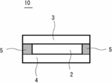
- the optical element 10 of this embodiment is a bendable element in which a substance having an optical effect is sandwiched between a pair of flexible substrates 3 and 4 as shown in FIGS. 1 is a view of the optical element viewed in the display direction, FIG. 2 is a cross-sectional view taken along line II-II in FIG. 1, and FIG. 3 is a cross-sectional view taken along line III-III in FIG. Between the pair of substrates 3 and 4, the sealing materials 1 and 5 having different elastic moduli for sealing substances having an optical effect are provided.
- the sealing materials 1 and 5 having different elastic moduli are formed in a rectangular shape along the shapes of the substrates 3 and 4, and the optical element 10 is bent on the long side and not on the short side. Composed. That is, the pair of long-side sealing materials 5 are bent and the pair of short-side sealing materials 1 are not bent.
- the elastic modulus of the long-side sealing material 5 and the short-side sealing material 1 are configured. The elastic modulus is different.
- along the bending direction of the optical element 10 that is, the sealing material 5 on the long side is easy to bend by placing a sealing material having a lower elastic modulus among the sealing materials having different elastic moduli. .
- This long side seal material 5 is parallel to the bending direction.
- At least one of the elastic moduli at room temperature after curing is in the range of 1 GPa to 2000 GPa, and the sealing material 5 having a lower elastic modulus disposed on the long side is the room temperature after curing.
- the sealing materials 1 and 5 having different elastic modulus are provided between the pair of substrates 3 and 4 as a substance having an optical effect, and the elastic modulus is different along the bending direction of the optical element 10.
- the sealing material 5 having a lower elastic modulus among the sealing materials 1 and 5, it becomes easy to add a curvature in one direction of the optical element 10.
- peeling between the substrates 3 and 4 due to bending is unlikely to occur, and destruction of the element due to bending and twisting of the optical element 10 is unlikely to occur in practice and in the production process.
- a pair of long-side sealing materials 5 are simultaneously applied to at least one substrate 4 of a pair of substrates, and a pair of short-side sealing materials 1 are simultaneously performed.
- a rectangular shape is formed in accordance with the shape of the substrate 4.
- the liquid crystal material 2 is injected into a region surrounded by the sealing materials 1 and 5 having different elastic moduli, the other substrate 3 is bonded to one substrate 4, and the liquid crystal material 2 is narrowed between the pair of substrates 3 and 4. Hold it.
- the substance having an optical effect is the liquid crystal material 2, which is used as a liquid crystal display element, but is also used for an EL element, a microcapsule element, an electropowder fluid element, an electrowetting element, an electrophoretic element, and the like. Can do.
- the optical element 10 of this embodiment is provided with sealing materials 1 and 5 having different elastic moduli for sealing substances having an optical effect between a pair of substrates 3 and 4.
- the structure is the same as that of the first embodiment, and the same reference numerals are given to omit the description.
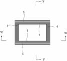
- 4 is a view of the optical element viewed in the display direction
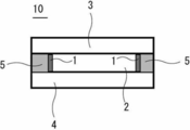
- FIG. 5 is a cross-sectional view taken along line VV in FIG. 4
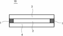
- FIG. 6 is a cross-sectional view taken along line VI-VI in FIG.
- the sealing material 1 is formed in a rectangular shape along the shapes of the substrates 3 and 4, the sealing material 5 having a different elastic modulus is provided on the outer side along the long side of the sealing material 1, and the long side Is configured so that the short side is not bent.
- at least one of the sealing materials having different elastic moduli has an elastic modulus at room temperature after curing of 1 GPa to 2000 GPa, and the sealing material 5 having different elastic moduli is elastic at room temperature after curing.
- the rate is in the range of 1 MPa to 1000 MPa.
- the sealing material 5 having a different elastic modulus is provided on the outer side along the long side of the sealing material 1, so that the sealing material 5 on the long side is a sealing material having a lower elastic modulus and is easily bent. It has become.
- the sealing material 1 for sealing a substance having an optical effect is drawn in a rectangular shape on at least one substrate 4 of a pair of substrates according to the shape of the substrate 4. After the sealing material 1 was drawn, the sealing material 5 was drawn in parallel on the pair of long sides.
- the optical element 10 of this embodiment is provided with sealing materials 1 and 5 having different elastic moduli for sealing substances having an optical effect between a pair of substrates 3 and 4.
- the structure is the same as that of the first embodiment, and the same reference numerals are given to omit the description.
- 7 is a view of the optical element viewed in the display direction
- FIG. 8 is a cross-sectional view taken along line VIII-VIII in FIG. 7
- FIG. 9 is a cross-sectional view taken along line IX-IX in FIG.
- the sealing material 5 is configured such that the short side is only the sealing material 1 and the long side is sandwiched between the sealing materials 1.
- the sealing materials 1 and 5 are drawn first in a rectangular shape in accordance with the shape of the substrate 4. After the sealing material 1 is drawn, a pair of long sides is drawn. The sealing material 5 was drawn in parallel on the side. Then, the sealing material 1 was again drawn on the sealing material 1 and the sealing material 5 drawn earlier.
- a transparent electrode or a connection terminal pattern made of ITO or the like is formed on the substrate 3 and the substrate 4 by sputtering and then patterned by photolithography.
- the substrate 4 is a polymer film excellent in heat resistance such as polysulfone or a polymer film reinforced with an inorganic material.
- a polyimide alignment film or the like is formed in advance by a printing method and subjected to an alignment treatment. Further, spacers are formed on the substrate 4. The spacer is patterned by photolithography.
- an application tool such as a dispenser is applied to the sealing member 1 or 5 made of an ultraviolet curable resin, a resin curable by a combination of ultraviolet rays and heat, or a thermosetting resin such as an acrylic resin or an epoxy resin on the substrate 4. Is used to form a rectangular frame.
- the liquid crystal material 2 is supplied to the substrate 4 by the dropping injection method. That is, the liquid crystal material 2 is dropped inside the rectangular frame-shaped sealing members 1 and 5 formed on the surface of the substrate 4.
- the substrate 3 was superposed under vacuum on the substrate 4 on which the liquid crystal was dropped.
- Example 4 A fourth embodiment will be described with reference to FIGS. It was produced in the same manner as in Example 1 except that the sealing material 1 and the sealing material 5 were allowed to coexist on the long side. The improvement by the constant temperature and humidity test was seen with respect to Example 1, and the effect with respect to seal peeling was confirmed compared with Example 2. The results are shown in the table of FIG.
- Example 5 is a case where C was used for the sealing material 1 and deteriorated with respect to seal peeling. The results are shown in the table of FIG.
- Example 6 A sixth embodiment will be described with reference to FIGS. It was produced in the same manner as in Example 1 except that the sealing material 1 and the sealing material 5 were applied on the long side. The seal peeling was improved with respect to Example 4, and it was possible to achieve both flexibility with respect to bending and display reliability. The results are shown in the table of FIG.
- the present invention can be bent and is less likely to be peeled off between the substrates due to bending, and is practically applied to the optical element in the production process such as application to the roll-to-roll method.
- the present invention can be applied to an optical element that does not easily break.
Landscapes
- Physics & Mathematics (AREA)
- Nonlinear Science (AREA)
- General Physics & Mathematics (AREA)
- Optics & Photonics (AREA)
- Mathematical Physics (AREA)
- Chemical & Material Sciences (AREA)
- Crystallography & Structural Chemistry (AREA)
- Liquid Crystal (AREA)
- Devices For Indicating Variable Information By Combining Individual Elements (AREA)
Abstract
曲げることが可能であり、しかも曲げによる基板間の剥れが生じにくく、実用上においてもロールツウロール法への適用など生産工程においても光学素子に対する曲げ、捩じりによる素子の破壊が生じにくい光学素子を提供する。 一対の可撓性を有する基板間に光学効果を有する物質を狭持した曲げ可能な光学素子(10)であり、一対の基板間に光学効果を有する物質をシールする弾性率の異なるシール材(1、5)を設け、光学素子の曲げ方向に沿って、弾性率の異なるシール材のうち、弾性率のより低いシール材(5)を配置した。弾性率の異なるシール材のうち、少なくとも1つは硬化後の室温における弾性率が1GPa~2000GPaの範囲である。また、弾性率のより低いシール材(5)は硬化後の室温における弾性率が1MPa~1000MPaの範囲である。
Description
この発明は、例えば、液晶層や有機EL層等の光学効果を有する物質を挟む一対の基板を曲げることが可能であり、しかも耐久性を有する光学素子に関する。
光学効果を有する物質を狭持した光学素子として、液晶表示素子、EL素子、マイクロカプセル素子、電子粉流体素子、エレクトロウェッティング素子、電気泳動素子などが知られている。このような光学素子は、例えば携帯電話、PDA(Personal Digital Assistants)、パブリックディスプレイなどに用いられ、一対のガラス基板が所定の間隔を空けて対向するように環状のシール材を用いて貼り合わせ、ガラス基板間に光学効果を有する物質を狭持したものが一般に用いられている(特許文献1)。
近年、軽量化あるいはフレキシブル化を目的として、従来のガラス基板に換えてポリイミドフィルム等のプラスチックフィルムを基板として使用する試みが行われている。また、このようなフレキシブル基板を用いた光学素子を製造する方法として、ロールツウロール(Roll to Roll)法が製造効率向上の観点から注目されている。ロールツウロール法では、背面基板と前面基板とを貼り合せた後にロール状に巻き取られるために、貼り合わせ後はロールの曲率半径で光学素子が保持される。また、本方式で作製された光学素子はフレキシブルな曲げ性を生かした用途が想定される。
以上の要求を満足するためには、光学素子自体の可撓性と曲げによって起こる基板の剥れや浮きあがりなど素子の破壊に対する耐久性とを両立する必要がある。
この発明が解決しようとする課題は、かかる実情に鑑みてなされたもので、曲げることが可能であり、しかも曲げによる基板間の剥れが生じにくく、実用上においてもロールツウロール法への適用など生産工程においても光学素子に対する曲げ、捩じりによる素子の破壊が生じにくい光学素子を提供することである。
前記課題を解決し、かつ目的を達成するために、この請求項1乃至請求項5に記載の発明は、以下のように構成した。
例えば、セルギャップが5μmの曲げ可能な光学素子を曲げた際、曲率半径100mmで一対の可撓性を有する基板で横方向に0.05×10⁻³(曲率半径100mmにおける一対の可撓性を有する基板のそれぞれの長さの差/光学素子の長辺(曲げ方向)の長さ)のズレが生じる。これにシール材の弾性率を乗ずることで応力を見積もることができ、シール材の弾性率が小さい程、曲げによって生ずる応力が小さくなる。曲げた状態で光学素子を固定する場合、曲げによって生ずる応力が小さい方が素子破壊の懸念が小さいことは明らかである。
例えば、特開2000-066220号公報において、125℃におけるシール材硬化物の弾性率が300MPa~2000MPaであることが望ましいことが開示され、2000MPa以下が望ましい理由としてシール材が非常に硬くて脆いため、液晶素子の落下による耐衝撃性試験ではシール材とガラス基板の間に亀裂が入り剥離が生ずることが挙げられる。しかし、この発明ではガラス基板ではなく可撓性を有する基板を用いるため2000MPa以上の弾性率においても耐衝撃性試験での不具合は生じない。
発明者らが鋭意検討した結果、可撓性を有する基板を用いた光学素子を曲げる場合に適したシール材の組み合わせが存在することを見出した。すなわち、一対の基板間に光学効果を有する物質をシールする弾性率の異なるシール材を設け、光学素子の曲げ方向に沿って、弾性率の異なるシール材のうち、弾性率のより低いシール材を配置した。
具体的には、曲げ方向の垂直方向に描画するシール材は硬化後の室温における弾性率で1GPa~2000GPaの範囲であることで表示信頼性を保ち、曲げ方向の並行方向に描画するシール材の少なくとも一種が硬化後の室温における弾性率で1MPa~1000MPaの範囲であることで曲げによる破壊が起こらない光学素子を提供できる。
また、曲げ方向の並行方向には、1MPa~1000MPaの硬化後の室温における弾性率と曲げに影響しない範囲で1GPa~2000GPaのシール材を共存させても良い。具体的には、光学素子の外周を硬化後の室温における弾性率が1GPa~2000GPaのシール材で切れ目なく最初に描画し、曲げ方向の二辺に更に硬化後の室温における弾性率が1MPa~1000MPaのシール材を重ねる、もしくは曲げ方向の二辺の外側に描画しても良い。これにより表示信頼性と曲げによる破壊に強い表示素子を提供することが可能となり、また、最初に表示素子の外周を描画することでシール欠陥の発生による歩留まりの低下を防ぐことができ、製造方法の観点からも有用な方法である。
前記構成により、この発明は、以下のような効果を有する。
請求項1乃至請求項5に記載の発明では、一対の基板間に光学効果を有する物質をシールする弾性率の異なるシール材を設け、光学素子の曲げ方向に沿って、弾性率の異なるシール材のうち、弾性率のより低いシール材を配置したことで、光学素子の一方向へ曲率を付加することが容易となる。しかも、曲げによる基板間の剥れが生じにくく、実用上においてもロールツウロール法への適用など生産工程においても光学素子に対する曲げ、捩じりによる素子の破壊が生じにくい。
以下、この発明の光学素子の実施の形態について説明する。この発明の実施の形態は、発明の最も好ましい形態を示すものであり、この発明はこれに限定されない。
[第1の実施の形態]
この実施の形態の光学素子10は、図1乃至図3に示すように、一対の可撓性を有する基板3,4間に光学効果を有する物質を狭持した曲げ可能な素子であり、図1は光学素子を表示方向に見た図、図2は図1のII-II線に沿う断面図、図3は図1のIII-III線に沿う断面図である。一対の基板3,4間には、光学効果を有する物質をシールする弾性率の異なるシール材1,5を設けた構造である。
この実施の形態の光学素子10は、図1乃至図3に示すように、一対の可撓性を有する基板3,4間に光学効果を有する物質を狭持した曲げ可能な素子であり、図1は光学素子を表示方向に見た図、図2は図1のII-II線に沿う断面図、図3は図1のIII-III線に沿う断面図である。一対の基板3,4間には、光学効果を有する物質をシールする弾性率の異なるシール材1,5を設けた構造である。
この実施の形態では、弾性率の異なるシール材1,5が基板3,4の形状に沿って矩形に形成され、この光学素子10は、長辺側を曲げ、短辺側は曲げないように構成される。すなわち、一対の長辺側のシール材5を曲げ、一対の短辺側のシール材1は曲げないように構成され、長辺側のシール材5の弾性率と、短辺側のシール材1の弾性率とが異なる。
このように、光学素子10の曲げ方向に沿って、すなわち、長辺側のシール材5は、弾性率の異なるシール材のうち、弾性率のより低いシール材を配置して曲げ易くなっている。この長辺側のシール材5は、曲げ方向と並行になっている。
このように、光学素子10の曲げ方向に沿って、すなわち、長辺側のシール材5は、弾性率の異なるシール材のうち、弾性率のより低いシール材を配置して曲げ易くなっている。この長辺側のシール材5は、曲げ方向と並行になっている。
この弾性率の異なるシール材のうち、少なくとも1つは硬化後の室温における弾性率が1GPa~2000GPaの範囲であり、長辺側に配置される弾性率のより低いシール材5は硬化後の室温における弾性率が1MPa~1000MPaの範囲であり、長辺側が曲げやすく、短辺側は曲げ難くなっている。
このように、一対の基板3,4間に光学効果を有する物質として液晶材料2をシールする弾性率の異なるシール材1,5を設け、光学素子10の曲げ方向に沿って、弾性率の異なるシール材1,5のうち、弾性率のより低いシール材5を配置したことで、光学素子10の一方向へ曲率を付加することが容易となる。しかも、曲げによる基板3,4間の剥れが生じにくく、実用上においても生産工程においても光学素子10に対する曲げ、捩じりによる素子の破壊が生じにくい。
この実施の形態の光学素子10の製造では、一対の基板の少なくとも1枚の基板4に、一対の長辺側のシール材5を同時に行い、また一対の短辺側のシール材1を同時に行い、基板4の形状に合わせて矩形状に形成される。この弾性率の異なるシール材1,5に囲まれた領域に、液晶材料2を注入し、一方の基板4に他方の基板3を貼り合わせ、一対の基板3,4間に液晶材料2を狭持する。
この実施の形態では、光学効果を有する物質が液晶材料2であり、液晶表示素子として用いるが、EL素子、マイクロカプセル素子、電子粉流体素子、エレクトロウェッティング素子、電気泳動素子などにも用いることができる。
[第2の実施の形態]
この実施の形態の光学素子10は、図4乃至図6に示すように、一対の基板3,4間には、光学効果を有する物質をシールする弾性率の異なるシール材1,5を設けた構造であり、第1の実施の形態と同じ構成は同じ符号を付して説明を省略する。図4は光学素子を表示方向に見た図、図5は図4のV-V線に沿う断面図、図6は図4のVI-VI線に沿う断面図である。
この実施の形態の光学素子10は、図4乃至図6に示すように、一対の基板3,4間には、光学効果を有する物質をシールする弾性率の異なるシール材1,5を設けた構造であり、第1の実施の形態と同じ構成は同じ符号を付して説明を省略する。図4は光学素子を表示方向に見た図、図5は図4のV-V線に沿う断面図、図6は図4のVI-VI線に沿う断面図である。
この実施の形態では、シール材1が基板3,4の形状に沿って矩形に形成され、このシール材1の長辺側に沿って外側に弾性率の異なるシール材5を設け、長辺側を曲げ、短辺側は曲げないように構成される。この実施の形態では、弾性率の異なるシール材のうち、少なくとも1つは硬化後の室温における弾性率が1GPa~2000GPaの範囲であり、弾性率の異なるシール材5は、硬化後の室温における弾性率が1MPa~1000MPaの範囲である。
この実施の形態では、シール材1の長辺側に沿って外側に弾性率の異なるシール材5を設けることで、長辺側のシール材5は、弾性率のより低いシール材であり曲げ易くなっている。
この実施の形態の光学素子の製造では、一対の基板の少なくとも1枚の基板4に、光学効果を有する物質をシールするシール材1を基板4の形状に合わせて矩形状に描画する。シール材1の描画後に、一対の長辺側にシール材5の描画を並列に行った。
[第3の実施の形態]
この実施の形態の光学素子10は、図7乃至図9に示すように、一対の基板3,4間には、光学効果を有する物質をシールする弾性率の異なるシール材1,5を設けた構造であり、第1の実施の形態と同じ構成は同じ符号を付して説明を省略する。図7は光学素子を表示方向に見た図、図8は図7のVIII-VIII線に沿う断面図、図9は図7のIX-IX線に沿う断面図である。
この実施の形態の光学素子10は、図7乃至図9に示すように、一対の基板3,4間には、光学効果を有する物質をシールする弾性率の異なるシール材1,5を設けた構造であり、第1の実施の形態と同じ構成は同じ符号を付して説明を省略する。図7は光学素子を表示方向に見た図、図8は図7のVIII-VIII線に沿う断面図、図9は図7のIX-IX線に沿う断面図である。
この実施の形態では、短辺側がシール材1のみ、長辺側がシール材1に挟まれる形でシール材5が存在するように構成される。シール材1の長辺側に沿って重ねて弾性率の異なるシール材5を設けることで、長辺側のシール材1,5は、弾性率のより低いシール材となり、曲げ易くなっている。
この実施の形態の光学素子の製造では、シール材1,5の描画は、まず、シール材1を基板4の形状に合わせて矩形状に描画し、シール材1の描画後に、一対の長辺側にシール材5の描画を並列に行った。そして、再度シール材1を先に描画したシール材1及びシール材5に重ねて描画した。
(実施例1乃至実施例3)
<液晶表示素子の製造>
実施例1乃至実施例3を、図1乃至図3に基づいて説明する。基板3、基板4にITO等からなる透明電極や接続端子パターンを、スパッタ法により成膜した後に、フォトリソグラフィー法によりパターニングすることによって形成する。基板4はポリスルホンなどの耐熱性に優れたポリマーフィルムまたは無機材料により補強されたポリマーフィルムである。透明電極の表面には、ポリイミド配向膜等も印刷法により予め皮膜形成し配向処理する。更に、基板4に、スペーサを形成する。スペーサはフォトリソグラフィー法によりパターン形成する。
<液晶表示素子の製造>
実施例1乃至実施例3を、図1乃至図3に基づいて説明する。基板3、基板4にITO等からなる透明電極や接続端子パターンを、スパッタ法により成膜した後に、フォトリソグラフィー法によりパターニングすることによって形成する。基板4はポリスルホンなどの耐熱性に優れたポリマーフィルムまたは無機材料により補強されたポリマーフィルムである。透明電極の表面には、ポリイミド配向膜等も印刷法により予め皮膜形成し配向処理する。更に、基板4に、スペーサを形成する。スペーサはフォトリソグラフィー法によりパターン形成する。
その後、基板4の上に、紫外線硬化樹脂、又は紫外線及び熱の併用によって硬化する樹脂、又は熱硬化性樹脂、例えばアクリル樹脂やエポキシ樹脂等からなるシール部材1、5を、ディスペンサー等の塗布ツールを用いて矩形枠状に形成する。
次に、液晶材料2を滴下注入法によって基板4に供給する。すなわち、基板4の表面に形成した矩形枠状のシール部材1、5の内側に、液晶材料2を滴下する。
その後、基板3を液晶が滴下された基板4の上に真空下で重ね合わせた。
<液晶表示素子の曲率固定による耐久性試験結果>
短辺方向のシール材を1とし、長辺方向のシール材を5として、長辺方向で曲げることとした。曲率半径100mmの半円形のアクリル筒に沿って液晶表示素子を押さえ、短辺側をメンディングテープで固定した。シール材1とシール材5の種類と弾性率を図10の表に示し24時間、72時間経過後に、液晶表示素子を2枚の偏光板で挟み、シール剥れによる液晶漏れの有無を目視で確認した結果を図10の表に示した。シール剥れが無いものについては、同一条件の新しい液晶表示素子を用いて24時間の間、60℃、80%恒温恒湿試験を行った。その後、液晶表示素子を二枚の偏光板で挟んで観察して、液晶の配向状態が乱れている領域が存在するものを表示不良ありと判定した。結果を図10の表に併せて示した。
短辺方向のシール材を1とし、長辺方向のシール材を5として、長辺方向で曲げることとした。曲率半径100mmの半円形のアクリル筒に沿って液晶表示素子を押さえ、短辺側をメンディングテープで固定した。シール材1とシール材5の種類と弾性率を図10の表に示し24時間、72時間経過後に、液晶表示素子を2枚の偏光板で挟み、シール剥れによる液晶漏れの有無を目視で確認した結果を図10の表に示した。シール剥れが無いものについては、同一条件の新しい液晶表示素子を用いて24時間の間、60℃、80%恒温恒湿試験を行った。その後、液晶表示素子を二枚の偏光板で挟んで観察して、液晶の配向状態が乱れている領域が存在するものを表示不良ありと判定した。結果を図10の表に併せて示した。
(実施例4)
実施例4を、図4乃至図6に基づいて説明する。長辺側にシール材1とシール材5を共存させている以外は、実施例1と同様に作製した。実施例1に対して恒温恒湿試験での改善がみられ、実施例2と比較してシール剥れに対して効果が確認できた。結果を図11の表に示した。
実施例4を、図4乃至図6に基づいて説明する。長辺側にシール材1とシール材5を共存させている以外は、実施例1と同様に作製した。実施例1に対して恒温恒湿試験での改善がみられ、実施例2と比較してシール剥れに対して効果が確認できた。結果を図11の表に示した。
(実施例5)
実施例5は、シール材1にCを用いた場合であり、シール剥れに対して悪化した。結果を図11の表に併せて示した。
実施例5は、シール材1にCを用いた場合であり、シール剥れに対して悪化した。結果を図11の表に併せて示した。
(実施例6)
実施例6を、図7乃至図9に基づいて説明する。長辺側にシール材1とシール材5を重ねて塗布した以外は、実施例1と同様に作製した。実施例4に対してシール剥れについて改善がみられ、曲げに対する可撓性の付与と表示信頼性の両立が可能となった。結果を図12の表に示した。
実施例6を、図7乃至図9に基づいて説明する。長辺側にシール材1とシール材5を重ねて塗布した以外は、実施例1と同様に作製した。実施例4に対してシール剥れについて改善がみられ、曲げに対する可撓性の付与と表示信頼性の両立が可能となった。結果を図12の表に示した。
この発明は、曲げることが可能であり、しかも曲げによる基板間の剥れが生じにくく、実用上においてもロールツウロール法への適用など生産工程においても光学素子に対する曲げ、捩じりによる素子の破壊が生じにくい光学素子に適用可能である。
1,5 シール材
2 液晶材料
3,4 基板
10 光学素子
2 液晶材料
3,4 基板
10 光学素子
Claims (5)
- 一対の可撓性を有する基板間に光学効果を有する物質を狭持した曲げ可能な光学素子であり、
前記一対の基板間に前記光学効果を有する物質をシールする弾性率の異なるシール材を設け、
前記光学素子の曲げ方向に沿って、前記弾性率の異なるシール材のうち、弾性率のより低いシール材を配置したことを特徴とする光学素子。 - 前記弾性率の異なるシール材のうち、少なくとも1つは硬化後の室温における弾性率が1GPa~2000GPaの範囲であることを特徴とする請求項1に記載の光学素子。
- 前記弾性率のより低いシール材は硬化後の室温における弾性率が1MPa~1000MPaの範囲であることを特徴とする請求項1に記載の光学素子。
- 前記光学素子の曲げ方向に沿って、前記弾性率の異なるシール材を2以上併用して配置したことを特徴とする請求項1乃至請求項3のいずれか1項に記載の光学素子。
- 前記光学効果を有する物質が液晶であることを特徴とする請求項1乃至請求項4のいずれか1項に記載の光学素子。
Applications Claiming Priority (2)
| Application Number | Priority Date | Filing Date | Title |
|---|---|---|---|
| JP2011050354A JP5791098B2 (ja) | 2011-03-08 | 2011-03-08 | 光学素子 |
| JP2011-050354 | 2011-03-08 |
Publications (1)
| Publication Number | Publication Date |
|---|---|
| WO2012120665A1 true WO2012120665A1 (ja) | 2012-09-13 |
Family
ID=46797666
Family Applications (1)
| Application Number | Title | Priority Date | Filing Date |
|---|---|---|---|
| PCT/JP2011/055519 Ceased WO2012120665A1 (ja) | 2011-03-08 | 2011-03-09 | 光学素子 |
Country Status (2)
| Country | Link |
|---|---|
| JP (1) | JP5791098B2 (ja) |
| WO (1) | WO2012120665A1 (ja) |
Cited By (2)
| Publication number | Priority date | Publication date | Assignee | Title |
|---|---|---|---|---|
| CN104777678A (zh) * | 2015-04-20 | 2015-07-15 | 京东方科技集团股份有限公司 | 一种曲面显示面板、显示装置 |
| JP2021018407A (ja) * | 2019-07-19 | 2021-02-15 | 元太科技工業股▲分▼有限公司Prime View International Co.,Ltd. | 表示装置 |
Families Citing this family (5)
| Publication number | Priority date | Publication date | Assignee | Title |
|---|---|---|---|---|
| CN104914612B (zh) * | 2015-07-02 | 2017-12-08 | 京东方科技集团股份有限公司 | 曲面显示装置、制作曲面显示装置的方法及其电子设备 |
| CN105511171B (zh) * | 2016-02-03 | 2019-01-22 | 京东方科技集团股份有限公司 | 液晶显示面板及其制备方法、以及显示装置 |
| JP6894589B2 (ja) * | 2016-08-31 | 2021-06-30 | 天馬微電子有限公司 | 表示装置及び表示装置の製造方法 |
| CN108415195A (zh) * | 2017-02-10 | 2018-08-17 | 京东方科技集团股份有限公司 | 显示面板及其制作方法、显示装置 |
| CN109360831B (zh) * | 2018-10-29 | 2021-11-02 | 合肥京东方显示技术有限公司 | 显示面板及其制备方法 |
Citations (11)
| Publication number | Priority date | Publication date | Assignee | Title |
|---|---|---|---|---|
| JPH05307161A (ja) * | 1992-04-30 | 1993-11-19 | Idemitsu Kosan Co Ltd | 液晶表示パネルの製造方法 |
| JP2005213470A (ja) * | 2004-02-02 | 2005-08-11 | Nichiban Co Ltd | シール材 |
| WO2007020717A1 (ja) * | 2005-08-18 | 2007-02-22 | Jsr Corporation | 表示装置の製造方法及び表示装置の製造装置 |
| JP2007178706A (ja) * | 2005-12-28 | 2007-07-12 | Seiko Epson Corp | 電気光学装置及び電子機器 |
| WO2007083412A1 (ja) * | 2006-01-17 | 2007-07-26 | Sharp Kabushiki Kaisha | 液晶表示装置 |
| JP2008150550A (ja) * | 2006-12-20 | 2008-07-03 | Bridgestone Corp | 接着剤組成物 |
| JP2009115933A (ja) * | 2007-11-05 | 2009-05-28 | Mitsubishi Electric Corp | 液晶表示装置及びその製造方法 |
| WO2009072226A1 (ja) * | 2007-12-06 | 2009-06-11 | Sharp Kabushiki Kaisha | 可撓性を有する表示装置 |
| JP2010026372A (ja) * | 2008-07-23 | 2010-02-04 | Mitsubishi Electric Corp | 湾曲型液晶パネル及びその液晶パネルの製造方法 |
| JP2010181545A (ja) * | 2009-02-04 | 2010-08-19 | Hitachi Displays Ltd | 液晶表示装置 |
| JP2010230901A (ja) * | 2009-03-26 | 2010-10-14 | Technology Research Association For Advanced Display Materials | 表示装置の製造方法 |
-
2011
- 2011-03-08 JP JP2011050354A patent/JP5791098B2/ja not_active Expired - Fee Related
- 2011-03-09 WO PCT/JP2011/055519 patent/WO2012120665A1/ja not_active Ceased
Patent Citations (11)
| Publication number | Priority date | Publication date | Assignee | Title |
|---|---|---|---|---|
| JPH05307161A (ja) * | 1992-04-30 | 1993-11-19 | Idemitsu Kosan Co Ltd | 液晶表示パネルの製造方法 |
| JP2005213470A (ja) * | 2004-02-02 | 2005-08-11 | Nichiban Co Ltd | シール材 |
| WO2007020717A1 (ja) * | 2005-08-18 | 2007-02-22 | Jsr Corporation | 表示装置の製造方法及び表示装置の製造装置 |
| JP2007178706A (ja) * | 2005-12-28 | 2007-07-12 | Seiko Epson Corp | 電気光学装置及び電子機器 |
| WO2007083412A1 (ja) * | 2006-01-17 | 2007-07-26 | Sharp Kabushiki Kaisha | 液晶表示装置 |
| JP2008150550A (ja) * | 2006-12-20 | 2008-07-03 | Bridgestone Corp | 接着剤組成物 |
| JP2009115933A (ja) * | 2007-11-05 | 2009-05-28 | Mitsubishi Electric Corp | 液晶表示装置及びその製造方法 |
| WO2009072226A1 (ja) * | 2007-12-06 | 2009-06-11 | Sharp Kabushiki Kaisha | 可撓性を有する表示装置 |
| JP2010026372A (ja) * | 2008-07-23 | 2010-02-04 | Mitsubishi Electric Corp | 湾曲型液晶パネル及びその液晶パネルの製造方法 |
| JP2010181545A (ja) * | 2009-02-04 | 2010-08-19 | Hitachi Displays Ltd | 液晶表示装置 |
| JP2010230901A (ja) * | 2009-03-26 | 2010-10-14 | Technology Research Association For Advanced Display Materials | 表示装置の製造方法 |
Cited By (7)
| Publication number | Priority date | Publication date | Assignee | Title |
|---|---|---|---|---|
| CN104777678A (zh) * | 2015-04-20 | 2015-07-15 | 京东方科技集团股份有限公司 | 一种曲面显示面板、显示装置 |
| WO2016169277A1 (en) | 2015-04-20 | 2016-10-27 | Boe Technology Group Co., Ltd. | Curved display panel and display apparatus containing the same |
| US9964811B2 (en) | 2015-04-20 | 2018-05-08 | Boe Technology Group Co., Ltd. | Curved display panel and display apparatus containing the same |
| EP3286602A4 (en) * | 2015-04-20 | 2019-02-20 | Boe Technology Group Co. Ltd. | CURVED DISPLAY PANEL AND DISPLAY APPARATUS INCLUDING THE SAME |
| JP2021018407A (ja) * | 2019-07-19 | 2021-02-15 | 元太科技工業股▲分▼有限公司Prime View International Co.,Ltd. | 表示装置 |
| US11698569B2 (en) | 2019-07-19 | 2023-07-11 | E Ink Holdings Inc. | Display device |
| JP7374699B2 (ja) | 2019-07-19 | 2023-11-07 | 元太科技工業股▲分▼有限公司 | 表示装置 |
Also Published As
| Publication number | Publication date |
|---|---|
| JP5791098B2 (ja) | 2015-10-07 |
| JP2012185457A (ja) | 2012-09-27 |
Similar Documents
| Publication | Publication Date | Title |
|---|---|---|
| JP5791098B2 (ja) | 光学素子 | |
| CN101297233B (zh) | 液晶显示装置 | |
| EP2219169A1 (en) | Flexible display device | |
| JP2013504789A (ja) | 曲面状のディスプレイパネル製造方法 | |
| US20130088662A1 (en) | Display device | |
| CN101467194A (zh) | 显示装置及其制造方法 | |
| JP2003216059A (ja) | 表示素子およびその製造方法 | |
| JP2009115933A (ja) | 液晶表示装置及びその製造方法 | |
| CN103064552A (zh) | 触控面板显示器及其组装方法以及触控感测模块 | |
| KR20080073252A (ko) | 플렉서블 액정 디스플레이 | |
| WO2012105061A1 (ja) | 光学素子及び光学素子の製造方法 | |
| US20140293205A1 (en) | Display device and method of manufacturing the same | |
| WO2016088615A1 (ja) | 湾曲型表示パネルの製造方法 | |
| CN101021641B (zh) | 制造液晶显示器的方法以及通过该方法制造的液晶显示器 | |
| TWI515705B (zh) | 貼合材料、顯示元件及顯示元件的製造方法 | |
| JP5399805B2 (ja) | 表示装置 | |
| JP5109228B2 (ja) | 薄板ガラス積層体及び薄板ガラス積層体を用いた表示装置の製造方法 | |
| CN102369563B (zh) | 显示装置的制造方法 | |
| US20210325704A1 (en) | Display panel, method for manufacturing the same, and display device | |
| JP2011033912A5 (ja) | ||
| JP2013125261A (ja) | 液晶表示素子 | |
| JP5143659B2 (ja) | 強誘電性液晶表示素子の製造方法 | |
| JP2006267532A (ja) | シール部材及びそれを用いた液晶装置 | |
| JP2011022212A (ja) | 液晶表示素子 | |
| WO2017085846A1 (ja) | 表示装置及び表示装置の製造方法 |
Legal Events
| Date | Code | Title | Description |
|---|---|---|---|
| 121 | Ep: the epo has been informed by wipo that ep was designated in this application |
Ref document number: 11860164 Country of ref document: EP Kind code of ref document: A1 |
|
| NENP | Non-entry into the national phase |
Ref country code: DE |
|
| 32PN | Ep: public notification in the ep bulletin as address of the adressee cannot be established |
Free format text: NOTING OF LOSS OF RIGHTS PURSUANT TO RULE 112(1) EPC |
|
| 122 | Ep: pct application non-entry in european phase |
Ref document number: 11860164 Country of ref document: EP Kind code of ref document: A1 |