WO2012117778A1 - 半導体装置の製造方法および半導体装置 - Google Patents
半導体装置の製造方法および半導体装置 Download PDFInfo
- Publication number
- WO2012117778A1 WO2012117778A1 PCT/JP2012/051659 JP2012051659W WO2012117778A1 WO 2012117778 A1 WO2012117778 A1 WO 2012117778A1 JP 2012051659 W JP2012051659 W JP 2012051659W WO 2012117778 A1 WO2012117778 A1 WO 2012117778A1
- Authority
- WO
- WIPO (PCT)
- Prior art keywords
- film
- semiconductor film
- metal oxide
- semiconductor
- etching
- Prior art date
Links
- 239000004065 semiconductor Substances 0.000 title claims abstract description 555
- 238000004519 manufacturing process Methods 0.000 title claims description 78
- 229910044991 metal oxide Inorganic materials 0.000 claims abstract description 273
- 150000004706 metal oxides Chemical class 0.000 claims abstract description 271
- 239000000758 substrate Substances 0.000 claims abstract description 50
- 238000001039 wet etching Methods 0.000 claims abstract description 42
- 238000001312 dry etching Methods 0.000 claims abstract description 33
- 238000012545 processing Methods 0.000 claims abstract description 18
- 238000010438 heat treatment Methods 0.000 claims abstract description 8
- 238000005530 etching Methods 0.000 claims description 187
- 238000000034 method Methods 0.000 claims description 93
- QVGXLLKOCUKJST-UHFFFAOYSA-N atomic oxygen Chemical compound [O] QVGXLLKOCUKJST-UHFFFAOYSA-N 0.000 claims description 37
- 229910052760 oxygen Inorganic materials 0.000 claims description 37
- 239000001301 oxygen Substances 0.000 claims description 37
- 229910052738 indium Inorganic materials 0.000 claims description 33
- APFVFJFRJDLVQX-UHFFFAOYSA-N indium atom Chemical compound [In] APFVFJFRJDLVQX-UHFFFAOYSA-N 0.000 claims description 33
- 229910052733 gallium Inorganic materials 0.000 claims description 30
- 239000002245 particle Substances 0.000 claims description 28
- GYHNNYVSQQEPJS-UHFFFAOYSA-N Gallium Chemical compound [Ga] GYHNNYVSQQEPJS-UHFFFAOYSA-N 0.000 claims description 26
- JBQYATWDVHIOAR-UHFFFAOYSA-N tellanylidenegermanium Chemical compound [Te]=[Ge] JBQYATWDVHIOAR-UHFFFAOYSA-N 0.000 claims description 20
- 229910007541 Zn O Inorganic materials 0.000 claims description 11
- 239000013078 crystal Substances 0.000 claims description 11
- ATJFFYVFTNAWJD-UHFFFAOYSA-N Tin Chemical compound [Sn] ATJFFYVFTNAWJD-UHFFFAOYSA-N 0.000 claims description 10
- 229910052782 aluminium Inorganic materials 0.000 claims description 5
- XAGFODPZIPBFFR-UHFFFAOYSA-N aluminium Chemical compound [Al] XAGFODPZIPBFFR-UHFFFAOYSA-N 0.000 claims description 5
- 239000010408 film Substances 0.000 abstract description 712
- 239000010409 thin film Substances 0.000 abstract description 94
- 229910052751 metal Inorganic materials 0.000 abstract description 60
- 239000002184 metal Substances 0.000 abstract description 60
- 238000002425 crystallisation Methods 0.000 abstract description 36
- 230000008025 crystallization Effects 0.000 abstract description 36
- 239000000463 material Substances 0.000 abstract description 25
- 239000005001 laminate film Substances 0.000 abstract 1
- 230000001131 transforming effect Effects 0.000 abstract 1
- 239000010410 layer Substances 0.000 description 485
- XLOMVQKBTHCTTD-UHFFFAOYSA-N Zinc monoxide Chemical compound [Zn]=O XLOMVQKBTHCTTD-UHFFFAOYSA-N 0.000 description 78
- 239000011787 zinc oxide Substances 0.000 description 39
- MUBZPKHOEPUJKR-UHFFFAOYSA-N Oxalic acid Chemical compound OC(=O)C(O)=O MUBZPKHOEPUJKR-UHFFFAOYSA-N 0.000 description 36
- 230000015572 biosynthetic process Effects 0.000 description 29
- 229920002120 photoresistant polymer Polymers 0.000 description 25
- JAONJTDQXUSBGG-UHFFFAOYSA-N dialuminum;dizinc;oxygen(2-) Chemical compound [O-2].[O-2].[O-2].[O-2].[O-2].[Al+3].[Al+3].[Zn+2].[Zn+2] JAONJTDQXUSBGG-UHFFFAOYSA-N 0.000 description 23
- 238000000059 patterning Methods 0.000 description 20
- AMGQUBHHOARCQH-UHFFFAOYSA-N indium;oxotin Chemical compound [In].[Sn]=O AMGQUBHHOARCQH-UHFFFAOYSA-N 0.000 description 19
- AJNVQOSZGJRYEI-UHFFFAOYSA-N digallium;oxygen(2-) Chemical compound [O-2].[O-2].[O-2].[Ga+3].[Ga+3] AJNVQOSZGJRYEI-UHFFFAOYSA-N 0.000 description 18
- 229910001195 gallium oxide Inorganic materials 0.000 description 18
- 229910003437 indium oxide Inorganic materials 0.000 description 17
- PJXISJQVUVHSOJ-UHFFFAOYSA-N indium(iii) oxide Chemical compound [O-2].[O-2].[O-2].[In+3].[In+3] PJXISJQVUVHSOJ-UHFFFAOYSA-N 0.000 description 17
- 238000004544 sputter deposition Methods 0.000 description 16
- 229910007604 Zn—Sn—O Inorganic materials 0.000 description 15
- 238000005229 chemical vapour deposition Methods 0.000 description 14
- 235000006408 oxalic acid Nutrition 0.000 description 12
- 229910045601 alloy Inorganic materials 0.000 description 10
- 239000000956 alloy Substances 0.000 description 10
- 238000004549 pulsed laser deposition Methods 0.000 description 10
- 238000000576 coating method Methods 0.000 description 9
- 150000007522 mineralic acids Chemical class 0.000 description 9
- 150000007524 organic acids Chemical class 0.000 description 9
- 238000000206 photolithography Methods 0.000 description 9
- 239000000969 carrier Substances 0.000 description 8
- 238000007639 printing Methods 0.000 description 8
- 238000001552 radio frequency sputter deposition Methods 0.000 description 8
- VYPSYNLAJGMNEJ-UHFFFAOYSA-N silicon dioxide Inorganic materials O=[Si]=O VYPSYNLAJGMNEJ-UHFFFAOYSA-N 0.000 description 7
- PXHVJJICTQNCMI-UHFFFAOYSA-N Nickel Chemical compound [Ni] PXHVJJICTQNCMI-UHFFFAOYSA-N 0.000 description 6
- 229910020923 Sn-O Inorganic materials 0.000 description 6
- 238000010586 diagram Methods 0.000 description 6
- 239000011159 matrix material Substances 0.000 description 6
- 150000002736 metal compounds Chemical class 0.000 description 6
- KYKLWYKWCAYAJY-UHFFFAOYSA-N oxotin;zinc Chemical compound [Zn].[Sn]=O KYKLWYKWCAYAJY-UHFFFAOYSA-N 0.000 description 6
- 229910052814 silicon oxide Inorganic materials 0.000 description 6
- 239000011701 zinc Substances 0.000 description 6
- YVTHLONGBIQYBO-UHFFFAOYSA-N zinc indium(3+) oxygen(2-) Chemical compound [O--].[Zn++].[In+3] YVTHLONGBIQYBO-UHFFFAOYSA-N 0.000 description 6
- 239000004973 liquid crystal related substance Substances 0.000 description 5
- 150000002739 metals Chemical class 0.000 description 5
- 230000001133 acceleration Effects 0.000 description 4
- QTBSBXVTEAMEQO-UHFFFAOYSA-N acetic acid Substances CC(O)=O QTBSBXVTEAMEQO-UHFFFAOYSA-N 0.000 description 4
- 239000011651 chromium Substances 0.000 description 4
- 239000010949 copper Substances 0.000 description 4
- 230000006866 deterioration Effects 0.000 description 4
- 238000011161 development Methods 0.000 description 4
- 230000018109 developmental process Effects 0.000 description 4
- 239000007772 electrode material Substances 0.000 description 4
- 238000002955 isolation Methods 0.000 description 4
- 239000000203 mixture Substances 0.000 description 4
- 239000010936 titanium Substances 0.000 description 4
- 229910052725 zinc Inorganic materials 0.000 description 4
- ZOKXTWBITQBERF-UHFFFAOYSA-N Molybdenum Chemical compound [Mo] ZOKXTWBITQBERF-UHFFFAOYSA-N 0.000 description 3
- 238000004380 ashing Methods 0.000 description 3
- 230000005540 biological transmission Effects 0.000 description 3
- 230000007423 decrease Effects 0.000 description 3
- 230000000694 effects Effects 0.000 description 3
- 230000005669 field effect Effects 0.000 description 3
- 230000006870 function Effects 0.000 description 3
- 239000011521 glass Substances 0.000 description 3
- 229910052750 molybdenum Inorganic materials 0.000 description 3
- 239000011733 molybdenum Substances 0.000 description 3
- 150000004767 nitrides Chemical class 0.000 description 3
- 238000001020 plasma etching Methods 0.000 description 3
- BASFCYQUMIYNBI-UHFFFAOYSA-N platinum Chemical compound [Pt] BASFCYQUMIYNBI-UHFFFAOYSA-N 0.000 description 3
- 229910021420 polycrystalline silicon Inorganic materials 0.000 description 3
- 238000007740 vapor deposition Methods 0.000 description 3
- VYZAMTAEIAYCRO-UHFFFAOYSA-N Chromium Chemical compound [Cr] VYZAMTAEIAYCRO-UHFFFAOYSA-N 0.000 description 2
- RYGMFSIKBFXOCR-UHFFFAOYSA-N Copper Chemical compound [Cu] RYGMFSIKBFXOCR-UHFFFAOYSA-N 0.000 description 2
- KRHYYFGTRYWZRS-UHFFFAOYSA-N Fluorane Chemical compound F KRHYYFGTRYWZRS-UHFFFAOYSA-N 0.000 description 2
- VEXZGXHMUGYJMC-UHFFFAOYSA-N Hydrochloric acid Chemical compound Cl VEXZGXHMUGYJMC-UHFFFAOYSA-N 0.000 description 2
- BQCADISMDOOEFD-UHFFFAOYSA-N Silver Chemical compound [Ag] BQCADISMDOOEFD-UHFFFAOYSA-N 0.000 description 2
- QAOWNCQODCNURD-UHFFFAOYSA-N Sulfuric acid Chemical compound OS(O)(=O)=O QAOWNCQODCNURD-UHFFFAOYSA-N 0.000 description 2
- RTAQQCXQSZGOHL-UHFFFAOYSA-N Titanium Chemical compound [Ti] RTAQQCXQSZGOHL-UHFFFAOYSA-N 0.000 description 2
- NRTOMJZYCJJWKI-UHFFFAOYSA-N Titanium nitride Chemical compound [Ti]#N NRTOMJZYCJJWKI-UHFFFAOYSA-N 0.000 description 2
- 229910007610 Zn—Sn Inorganic materials 0.000 description 2
- 229910052804 chromium Inorganic materials 0.000 description 2
- 239000002131 composite material Substances 0.000 description 2
- 150000004696 coordination complex Chemical class 0.000 description 2
- 229910052802 copper Inorganic materials 0.000 description 2
- 230000003247 decreasing effect Effects 0.000 description 2
- 238000005401 electroluminescence Methods 0.000 description 2
- 238000010894 electron beam technology Methods 0.000 description 2
- 239000010931 gold Substances 0.000 description 2
- 239000012535 impurity Substances 0.000 description 2
- 229910052759 nickel Inorganic materials 0.000 description 2
- 239000002985 plastic film Substances 0.000 description 2
- 229920006255 plastic film Polymers 0.000 description 2
- 229910052709 silver Inorganic materials 0.000 description 2
- 239000004332 silver Substances 0.000 description 2
- 239000002356 single layer Substances 0.000 description 2
- 238000003860 storage Methods 0.000 description 2
- 229910052715 tantalum Inorganic materials 0.000 description 2
- GUVRBAGPIYLISA-UHFFFAOYSA-N tantalum atom Chemical compound [Ta] GUVRBAGPIYLISA-UHFFFAOYSA-N 0.000 description 2
- XOLBLPGZBRYERU-UHFFFAOYSA-N tin dioxide Chemical compound O=[Sn]=O XOLBLPGZBRYERU-UHFFFAOYSA-N 0.000 description 2
- 229910001887 tin oxide Inorganic materials 0.000 description 2
- 229910052719 titanium Inorganic materials 0.000 description 2
- WFKWXMTUELFFGS-UHFFFAOYSA-N tungsten Chemical compound [W] WFKWXMTUELFFGS-UHFFFAOYSA-N 0.000 description 2
- 229910052721 tungsten Inorganic materials 0.000 description 2
- 239000010937 tungsten Substances 0.000 description 2
- 206010021143 Hypoxia Diseases 0.000 description 1
- -1 In-Sn-O Chemical compound 0.000 description 1
- GRYLNZFGIOXLOG-UHFFFAOYSA-N Nitric acid Chemical compound O[N+]([O-])=O GRYLNZFGIOXLOG-UHFFFAOYSA-N 0.000 description 1
- 229910052581 Si3N4 Inorganic materials 0.000 description 1
- XUIMIQQOPSSXEZ-UHFFFAOYSA-N Silicon Chemical compound [Si] XUIMIQQOPSSXEZ-UHFFFAOYSA-N 0.000 description 1
- 229910021417 amorphous silicon Inorganic materials 0.000 description 1
- 239000003990 capacitor Substances 0.000 description 1
- 239000000470 constituent Substances 0.000 description 1
- PMHQVHHXPFUNSP-UHFFFAOYSA-M copper(1+);methylsulfanylmethane;bromide Chemical compound Br[Cu].CSC PMHQVHHXPFUNSP-UHFFFAOYSA-M 0.000 description 1
- 238000000151 deposition Methods 0.000 description 1
- 238000005516 engineering process Methods 0.000 description 1
- PCHJSUWPFVWCPO-UHFFFAOYSA-N gold Chemical compound [Au] PCHJSUWPFVWCPO-UHFFFAOYSA-N 0.000 description 1
- 229910052737 gold Inorganic materials 0.000 description 1
- 230000012447 hatching Effects 0.000 description 1
- 239000007788 liquid Substances 0.000 description 1
- 239000007769 metal material Substances 0.000 description 1
- 238000012986 modification Methods 0.000 description 1
- 230000004048 modification Effects 0.000 description 1
- 229910017604 nitric acid Inorganic materials 0.000 description 1
- TWNQGVIAIRXVLR-UHFFFAOYSA-N oxo(oxoalumanyloxy)alumane Chemical compound O=[Al]O[Al]=O TWNQGVIAIRXVLR-UHFFFAOYSA-N 0.000 description 1
- 229910052697 platinum Inorganic materials 0.000 description 1
- 229920000052 poly(p-xylylene) Polymers 0.000 description 1
- 239000010453 quartz Substances 0.000 description 1
- 230000003252 repetitive effect Effects 0.000 description 1
- 238000012827 research and development Methods 0.000 description 1
- 229910052594 sapphire Inorganic materials 0.000 description 1
- 239000010980 sapphire Substances 0.000 description 1
- 238000007789 sealing Methods 0.000 description 1
- 229910052710 silicon Inorganic materials 0.000 description 1
- 239000010703 silicon Substances 0.000 description 1
- HQVNEWCFYHHQES-UHFFFAOYSA-N silicon nitride Chemical compound N12[Si]34N5[Si]62N3[Si]51N64 HQVNEWCFYHHQES-UHFFFAOYSA-N 0.000 description 1
- 239000002210 silicon-based material Substances 0.000 description 1
- 238000005477 sputtering target Methods 0.000 description 1
- 239000013077 target material Substances 0.000 description 1
Images


Classifications
-
- H—ELECTRICITY
- H01—ELECTRIC ELEMENTS
- H01L—SEMICONDUCTOR DEVICES NOT COVERED BY CLASS H10
- H01L29/00—Semiconductor devices specially adapted for rectifying, amplifying, oscillating or switching and having potential barriers; Capacitors or resistors having potential barriers, e.g. a PN-junction depletion layer or carrier concentration layer; Details of semiconductor bodies or of electrodes thereof ; Multistep manufacturing processes therefor
- H01L29/66—Types of semiconductor device ; Multistep manufacturing processes therefor
- H01L29/68—Types of semiconductor device ; Multistep manufacturing processes therefor controllable by only the electric current supplied, or only the electric potential applied, to an electrode which does not carry the current to be rectified, amplified or switched
- H01L29/76—Unipolar devices, e.g. field effect transistors
- H01L29/772—Field effect transistors
- H01L29/78—Field effect transistors with field effect produced by an insulated gate
- H01L29/786—Thin film transistors, i.e. transistors with a channel being at least partly a thin film
- H01L29/7869—Thin film transistors, i.e. transistors with a channel being at least partly a thin film having a semiconductor body comprising an oxide semiconductor material, e.g. zinc oxide, copper aluminium oxide, cadmium stannate
-
- H—ELECTRICITY
- H01—ELECTRIC ELEMENTS
- H01L—SEMICONDUCTOR DEVICES NOT COVERED BY CLASS H10
- H01L29/00—Semiconductor devices specially adapted for rectifying, amplifying, oscillating or switching and having potential barriers; Capacitors or resistors having potential barriers, e.g. a PN-junction depletion layer or carrier concentration layer; Details of semiconductor bodies or of electrodes thereof ; Multistep manufacturing processes therefor
- H01L29/66—Types of semiconductor device ; Multistep manufacturing processes therefor
- H01L29/66007—Multistep manufacturing processes
- H01L29/66969—Multistep manufacturing processes of devices having semiconductor bodies not comprising group 14 or group 13/15 materials
Definitions
- the present invention relates to a method of manufacturing a semiconductor device and a semiconductor device, and more particularly to a technique effective when applied to a semiconductor device having a field effect transistor using a semiconductor film made of a metal oxide as a channel layer.
- a thin film transistor which is a kind of field effect transistor, can be formed on an insulating substrate such as glass, and is a device that plays an important role in electronics technology.
- amorphous silicon or polycrystalline silicon is widely used as a channel layer material for TFTs.
- TFTs using a semiconductor film made of a metal oxide as a channel layer have attracted attention as an alternative material for these silicon materials. Collecting.
- a semiconductor film made of a metal oxide has excellent characteristics as a channel layer, the use of the semiconductor film can improve the characteristics of the TFT.
- Many semiconductor films made of metal oxide can be formed at room temperature. Therefore, it can be used when forming a TFT on a so-called flexible substrate such as a plastic film having low heat resistance, and is considered as one of the promising candidates for the channel layer material of the TFT.
- Non-Patent Document 1 discloses a TFT using In—Ga—Zn—O as a channel layer.
- this document discloses that a region having a thickness of about 30 nm where the underlying channel layer is damaged is removed by wet etching when the source electrode and the drain electrode are dry-etched.
- Non-Patent Document 2 discloses a TFT using In—Ga—Zn—O as a channel layer.
- the source and drain electrodes are dried by forming an etch stopper layer of Cu—In—Ga—Zn—O (high resistance semiconductor) on the In—Ga—Zn—O channel layer. The damage at the time of etching is prevented from reaching the channel layer.
- the present inventor is engaged in research and development of a thin film transistor using a semiconductor film made of a metal oxide as described above as a channel layer.
- processing by dry etching is excellent in processing accuracy and processing speed, and is therefore a method that has high mass productivity and is widely used industrially. Therefore, it is difficult to avoid using such a sputtering method or dry etching method. Therefore, examination of an effective method for removing the damaged layer is eagerly desired.
- Non-Patent Document 1 discusses removing a damaged channel layer having a thickness of about 30 nm by wet etching as described above.
- Patent Document 2 as described above, an etch stopper layer is formed so that damage during dry etching of the source electrode and the drain electrode does not reach the channel layer.
- the thickness of the channel layer can vary if the region damaged by dry etching is simply removed by wet etching. That is, wet etching has low controllability, and when a large number of TFTs are formed in a large area, the thickness of the channel layer of each TFT varies. Since the thickness of the channel layer is an important parameter that affects the characteristics of the TFT, the variation in the TFT characteristics increases due to the variation in the thickness of the channel layer. As a result, there is a problem that the yield of the product decreases.
- Non-Patent Document 2 has a problem that the on-current of the TFT is reduced because a Cu—In—Ga—Zn—O layer having a high resistance is inserted between the channel layer and the source / drain electrodes. is there.
- an object of the present invention is to provide a method of manufacturing a semiconductor device having good characteristics.
- Another object of the present invention is to provide a semiconductor device having good characteristics.
- an object of the present invention is to provide a configuration of a semiconductor device capable of improving the characteristics of a top contact TFT which is easily damaged by etching during processing of a source / drain electrode.
- a method for manufacturing a semiconductor device shown in a representative embodiment includes: (a) forming a first semiconductor film made of a semiconductor containing a first metal oxide above a substrate; (B) forming a second semiconductor film made of a semiconductor containing a second metal oxide on the first semiconductor film; (c) the first semiconductor film and the second semiconductor film; (D) After the step (c), a step of forming a first conductive film on the second semiconductor film, and (e) after the step (d), A step of removing the first conductive film in the first region on the second semiconductor film by etching; and (f) removing the second semiconductor film in the first region by etching after the step (e). Between the step (c) and the step (f) (g Subjected to heat treatment in the first semiconductor film, a step of crystallizing the first semiconductor film.
- a method for manufacturing a semiconductor device shown in a representative embodiment includes (a) a step of forming a semiconductor layer above a substrate, and (b) on the semiconductor layer. Forming a first semiconductor film made of a semiconductor containing a first metal oxide; and (c) forming a second semiconductor film made of a semiconductor containing a second metal oxide on the first semiconductor film.
- a semiconductor device shown in a representative embodiment includes: (a) a first semiconductor film made of a polycrystalline semiconductor containing a first metal oxide disposed above a substrate; (B) a source electrode and a drain electrode disposed above the first semiconductor film and spaced apart with a first region on the first semiconductor film interposed therebetween; (c) a gate electrode; d) a transistor having a gate insulating film, and (e) a second semiconductor film made of a semiconductor containing a second metal oxide, the first semiconductor film, the source electrode, and the first A second semiconductor film disposed between the semiconductor film and the drain electrode. Further, (f) a semiconductor layer may be provided below the first semiconductor film.
- a semiconductor device with good characteristics can be manufactured.
- the characteristics can be improved.
- FIG. 7 is a fragmentary cross-sectional view showing the manufacturing process of the semiconductor device of First Embodiment;
- FIG. 7 is a plan view of relevant parts showing a manufacturing step of the semiconductor device of First Embodiment;
- FIG. 3 is a main-portion cross-sectional view showing the manufacturing process of the semiconductor device in Embodiment 1, which is subsequent to FIG. 1;
- FIG. 4 is a main-portion cross-sectional view showing the manufacturing process of the semiconductor device in Embodiment 1, which is subsequent to FIG. 3;
- FIG. 3 is a plan view of relevant parts showing the manufacturing process of the semiconductor device of the first embodiment, and showing the process following FIG. 2;
- FIG. 5 is a main-portion cross-sectional view showing the manufacturing process of the semiconductor device in Embodiment 1, which is subsequent to FIG. 4;
- FIG. 7 is a cross-sectional view showing a main part of another manufacturing step of the semiconductor device in the first embodiment, following the step shown in FIG. 6;
- FIG. 6 is a substantial part plan view showing a manufacturing process of the semiconductor device in the first embodiment, and is a relevant part plan view showing a process following FIG. 5;
- FIG. 8 is a cross-sectional view showing a main part of another manufacturing step of the semiconductor device in the first embodiment, following the step shown in FIG.
- FIG. 10 is a main-portion cross-sectional view showing the manufacturing process of the semiconductor device of Embodiment 2;
- FIG. 13 is a main-portion cross-sectional view showing the manufacturing process of the semiconductor device in Embodiment 2, which is subsequent to FIG. 12;
- FIG. 10 is a main-portion cross-sectional view showing the manufacturing process of the semiconductor device in Embodiment 2, which is subsequent to FIG. 12;
- FIG. 10 is a main-portion cross-sectional view showing the manufacturing process of the semiconductor device of Embodiment 2;
- FIG. 13 is a main-portion cross-sectional view showing the manufacturing process of the semiconductor device in Embodiment 2, which is subsequent to FIG. 12;
- FIG. 14 is a main-portion cross-sectional view showing the manufacturing process of the semiconductor device in Embodiment 2, which is subsequent to FIG. 13;
- FIG. 15 is a main-portion cross-sectional view showing the manufacturing process of the semiconductor device in Embodiment 2, which is subsequent to FIG. 14;
- FIG. 16 is a main-portion cross-sectional view showing the manufacturing process of the semiconductor device in Embodiment 2, which is subsequent to FIG. 15;
- FIG. 10 is a main-portion cross-sectional view showing the manufacturing process of the semiconductor device of Embodiment 3;
- FIG. 18 is a main-portion cross-sectional view showing the manufacturing process of the semiconductor device in Embodiment 3, which is subsequent to FIG. 17;
- FIG. 18 is a main-portion cross-sectional view showing the manufacturing process of the semiconductor device in Embodiment 3, which is subsequent to FIG. 17;
- FIG. 19 is a main-portion cross-sectional view showing the manufacturing process of the semiconductor device in Embodiment 3, which is subsequent to FIG. 18;
- FIG. 20 is a main-portion cross-sectional view showing the manufacturing process of the semiconductor device in Embodiment 3, which is subsequent to FIG. 19;
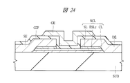
- FIG. 10 is a main-portion cross-sectional view showing the manufacturing process of the semiconductor device of Embodiment 4;
- FIG. 22 is a main-portion cross-sectional view showing the manufacturing process of the semiconductor device in Embodiment 4, which is subsequent to FIG. 21;
- FIG. 23 is a main-portion cross-sectional view showing the manufacturing process of the semiconductor device in Embodiment 4, which is subsequent to FIG. 22;
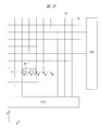
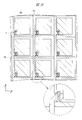
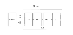
- FIG. 24 is a main-portion cross-sectional view showing the manufacturing process of the semiconductor device in Embodiment 4, which is subsequent to FIG. 23; It is a circuit diagram which shows the structure of an active matrix substrate. It is a top view which shows the structure of an active matrix substrate. It is a block diagram which shows the structure of an RFID tag.
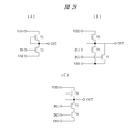
- 28A and 28B are circuit diagrams illustrating a logic circuit, in which FIG. 28A illustrates an inverter circuit, FIG. 28B illustrates a NOR circuit, and FIG. 28C illustrates a NAND circuit.
- the constituent elements are not necessarily indispensable unless otherwise specified or apparently indispensable in principle.
- the shapes when referring to the shapes, positional relationships, etc. of the components, etc., the shapes are substantially the same unless otherwise specified, or otherwise apparent in principle. And the like are included. The same applies to the above numbers and the like (including the number, numerical value, quantity, range, etc.).
- hatching may be omitted even in a cross-sectional view for easy understanding of the drawings. Further, even a plan view may be hatched to make the drawing easy to see.
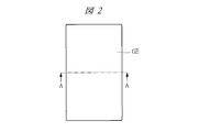
- FIG. 1 to 9 are main part sectional views or main part plan views showing manufacturing steps of the semiconductor device of the present embodiment.
- the cross-sectional view of the main part corresponds to the AA part of the main part plan view.
- FIG. 9 is one of main part sectional views showing the manufacturing process of the semiconductor device of the present embodiment.
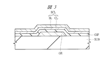
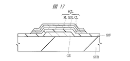
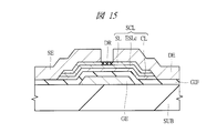
- the semiconductor device of this embodiment has a thin film transistor.
- This thin film transistor is a so-called bottom gate / top contact transistor.
- the bottom gate structure is a gate electrode below a semiconductor film that forms a channel (channel layer, here, a stacked film SCL of first and second metal oxide semiconductor films (conductive layer CLc and sacrificial layer SL)).
- This refers to the structure in which the GE is arranged.
- the top contact refers to a structure in which the source electrode SE and the drain electrode DE are disposed above the semiconductor film (here, the stacked film SCL).
- the thin film transistor of the present embodiment is disposed on the main surface of the substrate SUB.
- the thin film transistor of the present embodiment includes a gate electrode GE disposed on the substrate SUB, and the stacked film SCL that is a semiconductor film disposed on the gate electrode GE via the gate insulating film GIF; A source electrode SE and a drain electrode DE are disposed on the stacked film SCL.
- the source electrode SE and the drain electrode DE are arranged at a predetermined interval on the overlapping region of the gate electrode GE and the laminated film SCL.
- the portion having the predetermined interval becomes a channel region (first region).
- the semiconductor film includes a first metal oxide semiconductor film (conductive layer CLc, first semiconductor film) and a second metal oxide semiconductor film (sacrificial layer SL, second semiconductor film) disposed thereon.
- the upper second metal oxide semiconductor film (sacrificial layer SL) is removed.
- the first metal oxide semiconductor film (conductive layer CLc) is disposed in the channel region, and the first and second layers are disposed on both sides of the channel region, that is, below the source electrode SE and the drain electrode DE.
- a stacked film of metal oxide semiconductor films (conductive layer CLc and sacrificial layer SL) is disposed.
- the semiconductor film is formed of a stacked film (conductive layer CLc and sacrificial layer SL) and the upper layer film (here, sacrificial layer SL) is removed in the channel region. Transistor characteristics are improved.
- the sacrificial layer SL is removed from the semiconductor film in the channel region, damage is removed and the characteristics of the transistor can be improved.
- the lower layer film (here, the conductive layer CLc) has an etching rate (etch rate) of the upper layer film (here, the sacrificial layer SL). ) Is selected to be lower than the etching rate.
- the lower layer film (here, the conductive layer CLc) is crystallized (polycrystallized).
- the average grain size of the crystals is 1 nm or more. Therefore, the etching rate is reduced due to crystallization, and the film thickness and variation of the lower layer film (here, the conductive layer CLc) are reduced during the wet etching of the upper layer film (here, the sacrificial layer SL) in the stacked film. Can do.
- transistor characteristics can be improved.
- the mobility of carriers (electrons and holes) can be improved and the transistor characteristics can be improved.
- a glass substrate is prepared as the substrate SUB.
- the substrate SUB for example, a substrate made of quartz, sapphire or the like in addition to glass can be used. Further, a substrate made of a plastic film or the like, that is, a so-called flexible substrate may be used. If necessary, a substrate in which an insulating film is coated on the surface on which the gate electrode GE is formed may be used.
- the gate electrode material for example, a conductive film is deposited by sputtering or the like on the substrate SUB, and patterned into a predetermined shape (see FIG. 2), thereby forming the gate electrode GE.
- the gate electrode material include molybdenum (Mo), chromium (Cr), tungsten (W), aluminum (Al), copper (Cu), titanium (Ti), nickel (Ni), silver (Ag), and gold ( Metal materials such as Au), platinum (Pt), tantalum (Ta), and zinc (Zn) can be used. These may be used alone, or among these, several metals may be used as an alloy. Alternatively, a film in which the metal single layer or alloy layer is laminated may be used.
- a conductive metal oxide such as ITO (indium tin oxide, In—Sn—O, IndiumInTin Oxide) or aluminum zinc oxide (Al—Zn—O) may be used.
- a conductive metal nitride such as titanium nitride (TiN) can be used.
- a semiconductor containing impurities and having many carriers (electrons and holes) may be used.
- a stacked body of the above metal compound (metal oxide, metal nitride) or semiconductor and a metal (including an alloy) may be used.
- the gate electrode GE can be formed by vapor deposition or CVD (Chemical Vapor Deposition) as well as sputtering.
- the patterning can be performed by forming a photoresist film having a predetermined shape using a photolithography technique and then etching using the photoresist film as a mask. As this etching, dry etching or wet etching can be used.
- patterning may be performed by a so-called lift-off method in which the conductive film in a region other than the predetermined shape is removed together with the photoresist film. Good.
- a molybdenum film (Mo) having a thickness of about 100 nm is formed by vapor deposition using an electron beam (EB), and patterned by reactive ion etching (RIE (Reactive Ion Etching)).
- RIE reactive ion etching
- the shape of the gate electrode GE (planar shape viewed from above) is formed in a substantially rectangular shape having long sides in the first direction (vertical direction in the drawing), for example, as shown in FIG.
- a silicon oxide film (SiOx) is deposited on the gate electrode GE as a gate insulating film GIF by about 100 nm by a CVD method or the like.
- another oxide film such as an aluminum oxide film may be used. It is preferable to use these oxide films.
- an inorganic insulating film such as a silicon nitride film or an aluminum nitride film can be used. Further, an organic insulating film such as parylene may be used.
- a sputtering method, a coating method, or the like may be used as the film formation method.
- a first metal oxide semiconductor film is formed as a conductive layer (conductive film, semiconductor film, semiconductor layer) CL on the gate insulating film GIF.
- the conductive layer CL is a film constituting a main channel region of the thin film transistor and has a semiconductor property.
- an indium tin oxide (In—Sn—O, ITO: Indium ⁇ Tin ⁇ Oxide) film is deposited to a thickness of 5 nm or more by using, for example, an RF sputtering method.
- indium oxide (In—O) may be used in addition to the indium tin oxide (In—Sn—O).
- an oxide mainly composed of an oxide of In can be used.
- the film forming method is a film forming method in which a target is irradiated with laser light and a target material is deposited on a substrate placed on the surface of the target.
- the temperature at which the first metal oxide semiconductor film is formed is set to a temperature at which the metal oxide semiconductor film (conductive layer CL) does not crystallize (for example, 150 ° C. or less). That is, the metal oxide semiconductor film (conductive layer CL) is a non-crystalline (amorphous) film during film formation.
- a second metal oxide semiconductor film is formed as a sacrificial layer (conductive film, semiconductor film, semiconductor layer) SL on the conductive layer CL.
- This sacrificial layer SL is also a film having semiconductor properties.
- an indium gallium zinc oxide (In—Ga—Zn—O) film is deposited as the second metal oxide semiconductor film (sacrificial layer SL) by using, for example, an RF sputtering method.
- the thickness of the second metal oxide semiconductor film (sacrificial layer SL) is desirably set to 30 nm or more. This is because the depth of damage when the metal film MF described later is processed by dry etching is about 30 nm.
- the second metal oxide semiconductor film in addition to the indium gallium zinc oxide, zinc oxide (Zn—O), gallium oxide (Ga—O), zinc tin oxide (Zn—Sn—O), indium zinc oxide (In Zn or Ga-based oxides such as —Zn—O), gallium zinc oxide (Ga—Zn—O), indium gallium oxide (In—Ga—O), aluminum zinc oxide (Al—Zn—O), and the like
- other metal complex oxides can be used.
- a CVD method, a PLD method, a coating method, a printing method, or the like can be used as the film formation method.
- the temperature at which the second metal oxide semiconductor film is formed is such that the first metal oxide semiconductor film (conductive layer CL) is not crystallized at this time. ) Is preferably set to the above temperature at which crystallization does not occur (for example, 150 ° C. or lower).
- the sacrificial layer SL is made of any one of In—Ga—Zn—O, Zn—O, Al—Zn—O, Ga—Zn—O, and Zn—Sn—O. A combination is preferred. The reason will be described below.
- Indium tin oxide (In—Sn—O) has high practicality and versatility, and semiconductor characteristics can be easily realized by simply adjusting the oxygen content.
- indium tin oxide (In—Sn—O)
- a material containing about 10 wt% or less of Sn in In 2 O 3 is commercially available as a sputtering target for a transparent conductive film.
- the oxygen partial pressure it is possible to control whether the conductivity or the semiconductor characteristic is manifested by controlling the oxygen partial pressure. That is, increasing the oxygen partial pressure increases the amount of oxygen in the film (thus reducing the amount of carrier electrons), and continuously shifts from conductivity to semiconductor properties.
- the oxygen partial pressure is about 45 mPa
- the carrier electron density is about 5 ⁇ 10 19 cm ⁇ 3
- semiconductor characteristics begin to become apparent.
- the oxygen partial pressure is about 20 mPa or less, the conductivity becomes remarkable, and it can be used as a material for the gate electrode GE, the source electrode SE, and the drain electrode DE described later.
- each of In—Ga—Zn—O, Zn—O, Al—Zn—O, Ga—Zn—O, and Zn—Sn—O has an etching rate of polycrystalline.
- the etching rate of indium tin oxide (In—Sn—O) is higher than 0.1 nm / min. Specifically, for In—Ga—Zn—O (amorphous state), 12 nm / min, Zn—O (crystalline state) For Zn—Sn—O (amorphous state) is 15 nm / min (see FIG. 11). Note that the above data is data when an oxalic acid-based etching solution (specifically, ITO-07N manufactured by Kanto Chemical Co., Inc.) is used as the etching solution.
- the metal oxide is indicated by listing each element contained, and the composition ratio is not specified, but for these composition ratios, for example, desired characteristics, for example, If it is a semiconductor film, it may be a semiconductor characteristic, and if it is a conductive film, it may be a composition ratio having conductivity.
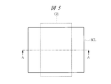
- the laminated film SCL is processed into an island shape for element isolation.
- a photoresist film (not shown) on a laminated film (laminated semiconductor film) SCL of first and second metal oxide semiconductor films (conductive layer CL and sacrificial layer SL), exposure / development processing (photolithography) )
- photolithography photolithography
- the laminated film having a desired shape is left by wet etching the laminated film using the photoresist film as a mask.
- the conductive layer CL is not crystallized (in an amorphous state), and its etching rate is large, 12 nm / min. Therefore, it is easy to etch.
- examples of the sacrificial layer SL include In—Ga—Zn—O, Zn—O, Al—Zn—O, Ga—Zn—O, and Zn—Sn—O, and others.
- the difference from the etching rate of (-Sn-O) is small (all are 10 times or less), and it is suitable for use as the sacrificial layer SL.
- the stacked film SCL of the first and second metal oxide semiconductor films has a shape (planar shape viewed from above) in the first direction (drawing), for example, as shown in FIG. It is formed in a substantially rectangular shape having a short side in the vertical direction).
- the stacked film SCL is formed in a shape having a region overlapping with the gate electrode GE. Note that processing of a film using such photolithography and etching techniques is sometimes referred to as patterning.
- the substrate SUB is subjected to heat treatment to crystallize the film below the stacked film SCL, that is, the first metal oxide semiconductor film (conductive layer CL).
- the first metal oxide semiconductor film (conductive layer) after crystallization is denoted by CLc.
- Crystallization here refers to polycrystallization so that the average particle diameter (diameter of crystal grains) is at least 1 nm or more.
- the lower limit of the average particle size is 1 nm, but in a typical case, the average particle size is about 20 nm.
- the average particle diameter (diameter of crystal grains) is a value measured using a transmission electron microscope or the like (the same applies to the following second to third embodiments).
- the heat processing temperature is 100 degreeC or more and 300 degrees C or less.
- the crystallization temperature of indium tin oxide (In—Sn—O) is about 150 ° C.
- the etching rate by the inorganic acid or the organic acid is 1/100 (1/100) of that before crystallization (amorphous state).
- the etching rate in the amorphous state is 12 nm / min.
- the etching rate becomes 0.1 nm / min (1/120) (see FIG. 11).
- the above data is data when an oxalic acid-based etching solution (specifically, ITO-07N manufactured by Kanto Chemical Co., Inc.) is used as the etching solution.
- a metal film MF is formed as a conductive film on the second metal oxide semiconductor film (sacrificial layer SL).
- the metal film MF includes, for example, molybdenum (Mo), chromium (Cr), tungsten (W), aluminum (Al), copper (Cu), titanium (Ti), nickel (Ni), tantalum (Ta), silver (Ag). ), Zinc (Zn), or other metal single layer films can be used.
- An alloy film containing two or more kinds of metals among the plurality of metals can be used.
- a laminated film of two or more kinds of films can be used among the metal film and the alloy film.
- a metal compound such as a conductive film made of a metal oxide such as ITO (Indium Tin Oxide, In-Sn-O, Indium Tin Oxide), or a conductive film made of a metal nitride such as titanium nitride (TiN).
- a conductive film may be used.
- a laminated film of a conductive film made of such a metal compound and the above metal film or alloy film may be used.
- a semiconductor film in which impurities are contained in a semiconductor film such as a polycrystalline silicon film and carriers (electrons, holes) are increased may be used.
- a stacked film of a semiconductor film such as a polycrystalline silicon film and the above metal film or alloy film may be used.
- the metal film or the alloy film can be formed using, for example, a sputtering method or a vapor deposition method.
- the semiconductor film can be formed using a CVD method or the like.
- the source electrode SE and the drain electrode DE are formed by patterning the metal film MF.
- This patterning can be performed by dry etching using the photoresist film as a mask by leaving the photoresist film in the formation region of the source electrode SE and the drain electrode DE using a photolithography technique.
- the second metal oxide semiconductor film (sacrificial layer SL) exposed from between the source electrode SE and the drain electrode DE is exposed to plasma and accelerated particles, so that a damaged region DR is formed.
- the source electrode SE and the drain electrode DE have a substantially rectangular shape as shown in FIG. 8, and are arranged at predetermined intervals on the overlapping region. ing. The portion having the predetermined interval becomes a channel region.
- the damage region DR described above is formed in a channel region that affects the characteristics of the thin film transistor.
- the lower second metal oxide semiconductor film (sacrificial layer SL) is formed using the lower source electrode SE and drain electrode DE as a mask. Remove by wet etching.
- an etchant containing an inorganic acid or an organic acid is used.
- the above-described oxalic acid-based etching solution ITO-07N manufactured by Kanto Chemical Co., Inc.
- the damaged region DR of the second metal oxide semiconductor film (sacrificial layer SL) is removed, and the lower first metal oxide semiconductor film (conductive layer CLc) is exposed from the channel region.
- the first metal oxide semiconductor film (conductive layer CLc) is difficult to be etched due to the crystallization, and the wet etching is automatically performed on the surface of the first metal oxide semiconductor film (conductive layer CLc). Almost stops. Further, even if the film thickness of the conductive layer CLc is reduced by wet etching, it is extremely small. In this process, since wet etching is used instead of dry etching, the first metal oxide semiconductor film (conductive layer CLc) is not exposed to plasma or acceleration particles generated during dry etching. Damage to the channel region of one metal oxide semiconductor film (conductive layer CLc) due to plasma or accelerated particles can be avoided.
- the thin film transistor of this embodiment is almost completed.
- the first metal oxide semiconductor film (conductive layer CL) is crystallized after patterning the stacked film SCL of the first and second metal oxide semiconductor films (conductive layer CL and sacrificial layer SL). Thereafter, the formation of the metal film MF and the patterning of the metal film MF are performed.
- the crystallization of the first metal oxide semiconductor film (conductive layer CL) is performed after the patterning step of the stacked film SCL, after the damage region DR (the first layer). The process may be performed until the removal step of the two-metal oxide semiconductor film (sacrificial layer SL)).
- the first metal oxide semiconductor film (conductive layer CL) may be crystallized after the formation process of the metal film MF or the dry etching process of the metal film MF.
- the semiconductor film is the stacked film SCL of the first and second metal oxide semiconductor films (the conductive layer CLc and the sacrificial layer SL), the damaged region DR can be removed. it can. Therefore, the characteristics of the thin film transistor can be improved by removing the damaged region DR.
- the etching rate of the lower first metal oxide semiconductor film (conductive layer CLc) decreases due to crystallization. Therefore, film loss due to the wet etching can be reduced.
- the film loss of the first metal oxide semiconductor film (conductive layer CLc) can be reduced.
- variations in the thickness of the lower first metal oxide semiconductor film (conductive layer CLc) serving as a main channel region can be suppressed, and variations in characteristics of the thin film transistor such as a threshold potential can be reduced.
- deterioration in characteristics of the thin film transistor can be reduced and the manufacturing yield of the semiconductor device can be improved.
- the semiconductor film is the stacked film SCL of the first and second metal oxide semiconductor films (the conductive layer CL and the sacrificial layer SL)
- the metal film MF constituting the source electrode SE and the drain electrode DE is formed, Even if damage due to plasma or accelerated particles is applied, the damage remains in the upper sacrificial layer SL, and damage applied to the first metal oxide semiconductor film (conductive layer CL) serving as a main channel layer can be reduced. .
- the characteristics of the thin film transistor can be improved.
- the second metal oxide semiconductor film (sacrificial layer SL) remains between the source electrode SE, the drain electrode DE, and the first metal oxide semiconductor film (conductive layer CLc).
- the second metal oxide semiconductor film (sacrificial layer SL) also has a semiconductor property and has a relatively low resistance during operation of the thin film transistor, the second metal oxide semiconductor film (sacrificial layer SL) has little influence on the operation characteristics of the thin film transistor.
- various semiconductors exemplified as the second metal oxide semiconductor film (sacrificial layer SL) are not high-resistance semiconductors such as Cu—In—Ga—Zn—O. Thus, reduction in on-state current of the thin film transistor can be suppressed.
- the carrier mobility is improved by crystallization of the first metal oxide semiconductor film (conductive layer CLc) as compared with the amorphous state, the on-state current of the thin film transistor can be improved.
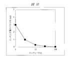
- FIG. 10 shows the etching amount of the first metal oxide semiconductor film (conductive layer CLc) relative to the etch rate ratio between the first metal oxide semiconductor film (conductive layer CLc) and the second metal oxide semiconductor film (sacrificial layer SL). It is a graph which shows the variation of.
- FIG. 11 is a table showing etch rates of various oxide materials with respect to the oxalic acid-based etching solution (specifically, ITO-07N manufactured by Kanto Chemical Co., Inc.).
- the allowable range of film thickness variation in the film forming process is about ⁇ 5%. Therefore, for example, when the film thickness of the second metal oxide semiconductor film (sacrificial layer SL) is 30 nm or more, there is a variation of 3 nm or more.
- the etching rate ratio (etch rate ratio) is 1, that is, the etching rate Er2 of the second metal oxide semiconductor film (sacrificial layer SL) and the first metal oxide semiconductor film (conductive layer).
- the etching rate Er1 of CLc is the same (Er2 / Er1 is 1), the thickness of the first metal oxide semiconductor film (conductive layer CLc) varies by 3 nm or more.
- the variation amount becomes 1/10 (1/10) 0.3 nm or more.
- the etching rate ratio is 100, that is, Er2 / Er1 is 100, the variation amount is 0.03 nm or more of 1/100 (1/100), and the variation amount is substantially close to 0 (zero). Value.
- an oxide material having an etching rate ratio (Er2 / Er1) of greater than 1, more preferably, 10 or greater is selected from the second metal oxide semiconductor film (sacrificial By selecting the layer SL), the amount of variation in the thickness of the first metal oxide semiconductor film (the conductive layer CLc, here, polycrystalline In—Sn—O) can be reduced.
- the first metal oxide semiconductor film (conductive layer CLc, here, polycrystalline In—Sn—O) has been described as an example.
- the first metal oxide semiconductor film is used.
- indium oxide (In—O) may be used.
- This indium oxide is also suitable for use as the first metal oxide semiconductor film (conductive layers CL and CLc) because the etching rate is lower in the polycrystalline state than in the amorphous state. Note that the crystallization temperature of indium oxide (In—O) is about 150 ° C.
- the second metal oxide semiconductor film (sacrificial layer SL) shown in FIG. 12, specifically, In—Ga—Zn—O, Zn—O, and Zn—Sn—O are examples, and the etching rate Er2
- another film may be used as long as it is a metal oxide semiconductor film that satisfies the relationship of greater than Er1 (Er2> Er1).
- Er1a a metal oxide semiconductor that satisfies Er1a> Er1 when the etching rate in the amorphous state is Er1a and the etching rate after crystallization is Er1.
- Other films may be used as long as they are films. Further, it is preferable that the difference between Er1a and Er2 is small.
- FIG. 11 the etching rate for ITO-07N manufactured by Kanto Chemical Co., Inc. is illustrated, but the same tendency is shown in the etching with inorganic acid or organic acid.
- the etchant besides ITO-07N manufactured by Kanto Chemical Co., Inc., hydrofluoric acid, hydrochloric acid, nitric acid, sulfuric acid, acetic acid, oxalic acid, or a mixture thereof can be used.
- the semiconductor film is a stacked film of two types of semiconductor films (conductive layer CL and sacrificial layer SL), but this semiconductor film may be a stacked film of three types of semiconductor films.
- 12 to 16 are main-portion cross-sectional views showing the manufacturing process of the semiconductor device of the present embodiment. Since the configuration of the laminated film SCL is different from that of the first embodiment, the configuration of the laminated film SCL and the manufacturing process thereof will be described in detail.
- FIG. 16 is one of main part cross-sectional views showing a manufacturing process of the semiconductor device of the present embodiment.
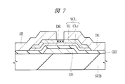
- the semiconductor device of this embodiment has a thin film transistor.
- This thin film transistor is a so-called bottom gate / top contact transistor.
- the thin film transistor of the present embodiment is disposed on the main surface of the substrate SUB.
- the thin film transistor of the present embodiment includes a gate electrode GE disposed on the substrate SUB, and the stacked film SCL that is a semiconductor film disposed on the gate electrode GE via the gate insulating film GIF; A source electrode SE and a drain electrode DE are disposed on the stacked film SCL.
- the source electrode SE and the drain electrode DE are arranged at a predetermined interval on the overlapping region of the gate electrode GE and the laminated film SCL.
- the portion having the predetermined interval becomes a channel region.
- the semiconductor film includes a metal oxide semiconductor film (conductive layer CL, semiconductor layer, main channel layer) and a first metal oxide semiconductor film (etching stopper layer ESLc, first semiconductor film) disposed thereon. ) And a second metal oxide semiconductor film (sacrificial layer SL, second semiconductor film) disposed thereon.
- the uppermost second metal oxide semiconductor film (sacrificial layer SL) is removed from the channel region.
- a two-layered film of the first metal oxide semiconductor film (etching stopper layer ESLc) and the metal oxide semiconductor film (conductive layer CL) is disposed, and both sides of the channel region, that is, A laminated film of three metal oxide semiconductor films (conductive layer CL, etching stopper layer ESLc, and sacrificial layer SL) is disposed below the source electrode SE and the drain electrode DE.
- the semiconductor film is formed of the three-layered film (conductive layer CL, etching stopper layer ESLc, and sacrificial layer SL) SCL, and the uppermost layer film (here, the sacrificial layer in the channel region). Since the layer SL) is removed, the transistor characteristics are improved.
- the sacrificial layer SL since the uppermost layer film (here, the sacrificial layer SL) is removed from the semiconductor film in the channel region, damage can be removed and the characteristics of the transistor can be improved. it can.
- the middle layer film (here, the etching stopper layer ESLc) is selected so that the etching rate is lower than the etching rate of the uppermost layer film (here, the sacrificial layer SL). Yes.
- the middle layer film (here, the etching stopper layer ESLc) is crystallized (polycrystallized) in the three-layered film SCL constituting the semiconductor film.
- the average grain size of the crystals is 1 nm or more. Accordingly, the etching rate is reduced by crystallization, and the middle layer film (here, the etching stopper layer ESLc) can function as an etching stopper when the upper layer film (here, the sacrificial layer SL) in the stacked film is wet etched.
- the selectivity of the lowermost layer film (here, the conductive layer CL) constituting the main channel layer is improved.
- the film having better semiconductor characteristics than the middle layer film (here, the etching stopper layer ESLc), for example, carrier A film having high mobility can be selected as appropriate and disposed in the lowermost layer. Thereby, the mobility of carriers (electrons and holes) can be improved and transistor characteristics can be improved.
- the gate insulating film GIF is formed on the gate electrode GE, as in the first embodiment. Since the formation method and materials of the gate electrode GE and the gate insulating film GIF are the same as those in the first embodiment, detailed description thereof is omitted.
- a metal oxide semiconductor film is formed as a conductive layer (conductive film, semiconductor film, semiconductor layer) CL on the gate insulating film GIF.
- the conductive layer CL is a film constituting a main channel region of the thin film transistor and has a semiconductor property.
- the metal oxide semiconductor film the metal compound semiconductor film described in Embodiment 1 (films exemplified as the conductive layer CL and the sacrificial layer SL in Embodiment 1), that is, indium oxide (In—O ), Indium zinc oxide (In—Zn—O), zinc oxide (Zn—O), gallium oxide (Ga—O), indium gallium zinc oxide (In—Ga—Zn—O), zinc tin oxide (Zn—Sn) —O), gallium zinc oxide (Ga—Zn—O), indium gallium oxide (In—Ga—O), aluminum zinc oxide (Al—Zn—O), tin oxide (Sn—O), etc. It can be selected and used.
- These film forming methods are as described in the first embodiment.
- the conductive layer CL is a film that constitutes the main channel region of the thin film transistor
- a metal oxide semiconductor film with good semiconductor characteristics may be selected as appropriate.
- the transistor characteristics can be improved by selecting a film having a semiconductor characteristic (for example, carrier mobility) that is at least better than that of an etching stopper (etch stopper) layer ESLc described later.
- a film having good film forming properties may be selected.
- transistor characteristics can be improved.
- a low cost film may be used. In this case, the manufacturing cost of the thin film transistor can be reduced.
- the conductive layer CL disposed in the lowermost layer of the stacked film SCL can be appropriately selected according to required performance and application.
- a first metal oxide semiconductor film is formed as an etching stopper layer ESL on the conductive layer CL.
- the etching stopper layer ESL has a semiconductor property.
- an indium tin oxide (In—Sn—O, ITO: Indium ⁇ Tin ⁇ Oxide) film is deposited to a thickness of 5 nm or more by using, for example, an RF sputtering method.
- indium oxide (In—O) may be used in addition to the indium tin oxide (In—Sn—O).
- an oxide mainly composed of an oxide of In can be used.
- the temperature at which the first metal oxide semiconductor film is formed is, for example, a temperature at which the metal oxide semiconductor film (conductive layer CL) does not crystallize (for example, 150 ° C. or less). That is, the metal oxide semiconductor film (conductive layer CL) is a non-crystalline (amorphous) film during film formation.
- a second metal oxide semiconductor film is formed as a sacrificial layer (conductive film, semiconductor film, semiconductor layer) SL on the etching stopper layer ESL.
- This sacrificial layer SL is also a film having semiconductor properties.
- the second metal oxide semiconductor film (sacrificial layer SL) for example, indium gallium zinc oxide (In—Ga—Zn—O) is deposited using, for example, an RF sputtering method.
- the thickness of the second metal oxide semiconductor film (sacrificial layer SL) is desirably set to 30 nm or more. This is because the depth of damage when the metal film MF described later is processed by dry etching is about 30 nm.
- the second metal oxide semiconductor film in addition to zinc oxide, zinc oxide (Zn—O), gallium oxide (Ga—O), zinc tin oxide (Zn—Sn—O), indium zinc oxide (In—Zn oxide) Zn or Ga-based oxides such as —O), gallium zinc oxide (Ga—Zn—O), indium gallium oxide (In—Ga—O), aluminum zinc oxide (Al—Zn—O), and others It is possible to use a composite oxide of these metals. In addition to the sputtering method, a CVD method, a PLD method, a coating method, a printing method, or the like can be used as the film formation method.
- the temperature at the time of forming the second metal oxide semiconductor film is such that the first metal oxide semiconductor film (etching stopper ESL) is not crystallized at this time.
- the temperature is such that the layer ESL) does not crystallize (for example, 150 ° C. or lower).
- the first metal oxide semiconductor film (etching stopper layer ESL) and the second metal oxide semiconductor film (sacrificial layer SL) various combinations of the above materials are conceivable.
- the ESL is made of In—Sn—O
- the sacrificial layer SL is made of any one of In—Ga—Zn—O, Zn—O, Al—Zn—O, Ga—Zn—O, and Zn—Sn—O. Such combinations are preferred.
- the reason is as described in the first embodiment (see FIG. 11 and the like).
- the laminated film SCL is processed into an island shape for element isolation.
- a photoresist film (not shown) is formed on the laminated film (laminated semiconductor film) SCL of the metal oxide semiconductor film, the first and second metal oxide semiconductor films (conductive layer CL, etching stopper layer ESL, and sacrificial layer SL).
- exposure / development processing photolithography
- the laminated film having a desired shape is left by wet etching the laminated film using the photoresist film as a mask.
- the etching stopper layer ESL is not crystallized (in an amorphous state), and the etching rate is high. Therefore, it is easy to etch.
- the sacrificial layer SL include In—Ga—Zn—O, Zn—O, Al—Zn—O, Ga—Zn—O, and Zn—Sn—O, and others.
- the difference from the etching rate of (-Sn-O) is small (both are 10 times or less) and is suitable for use as the sacrificial layer SL (see FIG. 11).
- the shape of the laminated film SCL (planar shape viewed from above) is formed in a substantially rectangular shape having a short side in the first direction (vertical direction in the drawing), as in the first embodiment (see FIG. 5).
- the stacked film SCL is formed in a shape having a region overlapping with the gate electrode GE.
- the substrate SUB is subjected to heat treatment to crystallize the lower layer film of the stacked film SCL, that is, the first metal oxide semiconductor film (etching stopper layer ESL).
- the first metal oxide semiconductor film (etching stopper layer ESL) after crystallization is indicated by ESLc.
- Crystallization here refers to polycrystallization so that the average particle diameter (diameter of crystal grains) is at least 1 nm or more.
- the lower limit of the average particle size is 1 nm, but in a typical case, the average particle size is about 20 nm.
- the heat processing temperature is 100 degreeC or more and 300 degrees C or less.
- the etching rate by the inorganic acid or the organic acid is 1/100 (1 / 100th of that before crystallization (amorphous state)).
- the etching rate in the amorphous state is 12 nm / min.
- the etching rate becomes 0.1 nm / min (1/120) (see FIG. 11).
- a metal film MF is formed as a conductive film on the second metal oxide semiconductor film (sacrificial layer SL).
- the metal film MF can be formed using, for example, the material described in Embodiment 1 by the film formation method described in Embodiment 1.
- the metal film MF is patterned in the same manner as in the first embodiment to form the source electrode SE and the drain electrode DE.
- the second metal oxide semiconductor film (sacrificial layer SL) exposed from between the source electrode SE and the drain electrode DE is exposed to plasma and accelerated particles, so that a damaged region DR is formed.
- the shape of the source electrode SE and the drain electrode DE (planar shape seen from the top surface) is substantially rectangular as in the first embodiment (see FIG. 8), and has a predetermined interval on the overlapping region. It is placed and placed. The portion having the predetermined interval becomes a channel region.
- the damage region DR described above is formed in a channel region that affects the characteristics of the thin film transistor.
- the lower second metal oxide semiconductor film (sacrificial layer SL) is removed by wet etching.
- the etchant an etchant containing an inorganic acid or an organic acid is used.
- the above-described oxalic acid-based etching solution ITO-07N manufactured by Kanto Chemical Co., Inc.
- the damaged region DR of the second metal oxide semiconductor film (sacrificial layer SL) is removed, and the lower first metal oxide semiconductor film (etching stopper layer ESLc) is exposed from the channel region.
- the first metal oxide semiconductor film (etching stopper layer ESLc) is difficult to be etched due to the crystallization, and the wet etching is automatically performed on the surface of the first metal oxide semiconductor film (etching stopper layer ESLc). Almost stop. Further, even if the thickness of the etching stopper layer ESLc is reduced by wet etching, it is very small.
- the first metal oxide semiconductor film (etching stopper layer ESLc) plays a role as an etching stopper, the lower metal oxide semiconductor film (conductive layer CL) is not affected by etching.
- the thin film transistor of this embodiment is almost completed.
- the first metal oxide semiconductor film (etching stopper layer ESL) was crystallized, and then the formation of the metal film MF and the patterning of the metal film MF were performed.
- the crystallization of the first metal oxide semiconductor film (etching stopper layer ESL) The process may be performed after the patterning process of the film SCL and before the process of removing the damaged region DR (second metal oxide semiconductor film (sacrificial layer SL)).
- the first metal oxide semiconductor film (etching stopper layer ESL) may be crystallized after the formation process of the metal film MF or the dry etching process of the metal film MF.
- the semiconductor film is a metal oxide semiconductor film, the stacked film SCL of the first and second metal oxide semiconductor films (the conductive layer CL, the etching stopper layer ESLc, and the sacrificial layer SL).
- the damaged region DR can be removed. Therefore, the characteristics of the thin film transistor can be improved by removing the damaged region DR.
- the etching rate of the lower first metal oxide semiconductor film is decreased by crystallization even when wet etching, which is generally considered to have low controllability, is used.
- it plays the role of an etching stopper, it reduces the film loss of itself and protects the underlying metal oxide semiconductor film (conductive layer CL).
- the first metal oxide semiconductor film is reduced in film thickness, and the lower layer The metal oxide semiconductor film (conductive layer CL) can be protected.
- the semiconductor film is a laminated film SCL of three layers (conductive layer CL, etching stopper layer ESLc, sacrificial layer SL), plasma and acceleration are performed when the metal film MF constituting the source electrode SE and the drain electrode DE is formed. Even if the damage due to the particles is applied, the damage remains in the uppermost sacrificial layer SL, and the metal oxide semiconductor film (conductive layer CL) or the first metal oxide semiconductor film (etching stopper layer ESLc) which becomes the main channel layer. ) Can be reduced. Thus, the characteristics of the thin film transistor can be improved.
- the first and second metal oxide semiconductor films are provided between the source electrode SE and drain electrode DE and the metal oxide semiconductor film (conductive layer CL).
- these films also have semiconductor properties and have a relatively low resistance during operation of the thin film transistor, there is little influence on the operation characteristics of the thin film transistor.
- various semiconductors exemplified as the first and second metal oxide semiconductor films (etching stopper layer ESLc and sacrificial layer SL) are not high resistance semiconductors such as Cu—In—Ga—Zn—O. . Thus, reduction in on-state current of the thin film transistor can be suppressed.
- the selection range of the lowermost metal oxide semiconductor is increased. That is, regardless of the etching rate, by selecting a desired semiconductor film, the semiconductor characteristics can be improved and the productivity can be improved.
- the two-layer semiconductor film (the conductive layer CL and the sacrificial layer SL) has been described using a so-called bottom gate / top contact transistor as an example.
- the sacrificial layer SL may be applied to a transistor having a top gate / top contact structure.
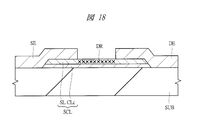
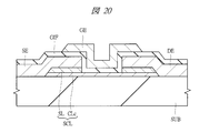
- 17 to 20 are main-portion cross-sectional views showing the manufacturing process of the semiconductor device of the present embodiment. Detailed description of the configuration and manufacturing process common to the first embodiment will be omitted.
- FIG. 20 is one of main part cross-sectional views showing a manufacturing process of the semiconductor device of the present embodiment.
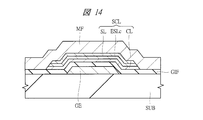
- the semiconductor device of this embodiment has a thin film transistor.
- This thin film transistor is a so-called top gate / top contact transistor.
- the top gate structure is a gate electrode formed above a semiconductor film that forms a channel (channel layer, here, a stacked film SCL of first and second metal oxide semiconductor films (conductive layer CLc and sacrificial layer SL)). This refers to the structure in which the GE is arranged.
- the top contact refers to a structure in which the source electrode SE and the drain electrode DE are disposed above the semiconductor film (here, the conductive layer CLc and the sacrificial layer SL).
- the thin film transistor of the present embodiment is disposed on the main surface of the substrate SUB.
- the thin film transistor of this embodiment includes the stacked film SCL that is a semiconductor film disposed on the substrate SUB, the source electrode SE and the drain electrode DE disposed on the stacked film SCL, and the source electrode SE. And a gate electrode GE disposed between the drain electrode DE via a gate insulating film GIF.
- the source electrode SE and the drain electrode DE are arranged at a predetermined interval on the laminated film SCL.
- a gate electrode GE is disposed on the predetermined interval via a gate insulating film GIF, and a portion of the predetermined interval becomes a channel region.
- the semiconductor film includes a first metal oxide semiconductor film (conductive layer CLc, first semiconductor film) and a second metal oxide semiconductor film (sacrificial layer SL, second semiconductor film) disposed thereon.
- the upper second metal oxide semiconductor film (sacrificial layer SL) is removed.
- the first metal oxide semiconductor film (conductive layer CLc) is disposed in the channel region, and the first and second layers are disposed on both sides of the channel region, that is, below the source electrode SE and the drain electrode DE.
- a stacked film of metal oxide semiconductor films (conductive layer CLc and sacrificial layer SL) is disposed.
- the semiconductor film is formed of a stacked film (conductive layer CLc and sacrificial layer SL) and the upper layer film (here, sacrificial layer SL) is removed in the channel region. Transistor characteristics are improved.
- the sacrificial layer SL is removed from the semiconductor film in the channel region, damage is removed and the characteristics of the transistor can be improved.
- the lower layer film (here, the conductive layer CLc) has an etching rate of the upper layer film (here, the sacrificial layer SL). Selected to be lower.
- the lower layer film (here, the conductive layer CLc) is crystallized (polycrystallized).
- the average grain size of the crystals is 1 nm or more. Therefore, the etching rate is reduced due to crystallization, and the film thickness and variation of the lower layer film (here, the conductive layer CLc) are reduced during the wet etching of the upper layer film (here, the sacrificial layer SL) in the stacked film. Can do.
- transistor characteristics can be improved.
- the mobility of carriers (electrons and holes) can be improved and the transistor characteristics can be improved.
- a substrate SUB is prepared as in the first embodiment.
- a first metal oxide semiconductor film is formed as a conductive layer (conductive film, semiconductor film, semiconductor layer) CL over the substrate SUB.
- the conductive layer CL is a film constituting a main channel region of the thin film transistor and has a semiconductor property.
- an indium tin oxide (In—Sn—O, ITO: Indium ⁇ Tin ⁇ Oxide) film is deposited to a thickness of 5 nm or more by using, for example, an RF sputtering method.
- indium oxide (In—O) may be used in addition to the indium tin oxide (In—Sn—O).
- an oxide mainly composed of an oxide of In can be used.
- the film forming method in addition to the sputtering method, a CVD method, a PLD method, a coating method, a printing method, and the like can be used.
- the temperature at which the first metal oxide semiconductor film is formed is set to a temperature at which the metal oxide semiconductor film (conductive layer CL) does not crystallize (for example, 150 ° C. or less). That is, the metal oxide semiconductor film (conductive layer CL) is a non-crystalline (amorphous) film during film formation.
- a second metal oxide semiconductor film is formed as a sacrificial layer (conductive film, semiconductor film, semiconductor layer) SL on the conductive layer CL.
- This sacrificial layer SL is also a film having semiconductor properties.
- an indium gallium zinc oxide (In—Ga—Zn—O) film is deposited as the second metal oxide semiconductor film (sacrificial layer SL) by using, for example, an RF sputtering method.
- the thickness of the second metal oxide semiconductor film (sacrificial layer SL) is desirably set to 30 nm or more. This is because the depth of damage when the metal film MF described later is processed by dry etching is about 30 nm.
- the second metal oxide semiconductor film in addition to the indium gallium zinc oxide, zinc oxide (Zn—O), gallium oxide (Ga—O), zinc tin oxide (Zn—Sn—O), indium zinc oxide (In Zn or Ga-based oxides such as —Zn—O), gallium zinc oxide (Ga—Zn—O), indium gallium oxide (In—Ga—O), aluminum zinc oxide (Al—Zn—O), and the like
- other metal complex oxides can be used.
- a CVD method, a PLD method, a coating method, a printing method, or the like can be used as the film formation method.
- the temperature at which the second metal oxide semiconductor film is formed is such that the first metal oxide semiconductor film (conductive layer CL) is not crystallized at this time. ) Is preferably set to the above temperature at which crystallization does not occur (for example, 150 ° C. or lower).
- the sacrificial layer SL is made of any one of In—Ga—Zn—O, Zn—O, Al—Zn—O, Ga—Zn—O, and Zn—Sn—O. A combination is preferred. The reason is as described in the first embodiment.
- the laminated film SCL is processed into an island shape for element isolation.
- a photoresist film (not shown) on a laminated film (laminated semiconductor film) SCL of first and second metal oxide semiconductor films (conductive layer CL and sacrificial layer SL), exposure / development processing (photolithography) )
- photolithography photolithography
- the laminated film having a desired shape is left by wet etching the laminated film using the photoresist film as a mask.
- the conductive layer CL is not crystallized (in an amorphous state), and the etching rate is high. Therefore, it is easy to etch.
- examples of the sacrificial layer SL include In—Ga—Zn—O, Zn—O, Al—Zn—O, Ga—Zn—O, and Zn—Sn—O, and others.
- the difference from the etching rate of (-Sn-O) is small (all are 10 times or less), and it is suitable for use as the sacrificial layer SL.
- the shape (planar shape seen from the top surface) of the laminated film SCL of the first and second metal oxide semiconductor films (the conductive layer CL and the sacrificial layer SL) is, for example, in the first direction ( It is formed in a substantially rectangular shape having a short side in the longitudinal direction (see FIG. 5).
- the substrate SUB is subjected to heat treatment to crystallize the film below the stacked film SCL, that is, the first metal oxide semiconductor film (conductive layer CL).
- the first metal oxide semiconductor film (conductive layer) after crystallization is denoted by CLc.
- Crystallization here refers to polycrystallization so that the average particle diameter (diameter of crystal grains) is at least 1 nm or more.
- the lower limit of the average particle size is 1 nm, but in a typical case, the average particle size is about 20 nm.
- the heat processing temperature is 100 degreeC or more and 300 degrees C or less.
- the etching rate by the inorganic acid or the organic acid is 1/100 (1/100) of that before crystallization (amorphous state).
- the etching rate in the amorphous state is 12 nm / min.
- the etching rate becomes 0.1 nm / min (1/120).
- a metal film MF is formed as a conductive film on the second metal oxide semiconductor film (sacrificial layer SL).
- the metal film MF can be formed using, for example, various materials such as the metal film and the alloy film described in detail in the first embodiment and the film formation method described in detail in the first embodiment.
- the metal film MF is patterned to form the source electrode SE and the drain electrode DE.
- This patterning can be performed by dry etching using the photoresist film as a mask by leaving the photoresist film in the formation region of the source electrode SE and the drain electrode DE using a photolithography technique.
- the second metal oxide semiconductor film (sacrificial layer SL) exposed from between the source electrode SE and the drain electrode DE is exposed to plasma and accelerated particles, so that a damaged region DR is formed.
- the shape of the source electrode SE and the drain electrode DE can be substantially rectangular (see FIG. 8), for example, as in the first embodiment. Are arranged at predetermined intervals. The portion having the predetermined interval becomes a channel region.
- the damage region DR described above is formed in a channel region that affects the characteristics of the thin film transistor.
- the underlying second metal oxide semiconductor film (sacrificial layer SL) is formed using the underlying source electrode SE and drain electrode DE as a mask. Remove by wet etching.
- an etchant containing an inorganic acid or an organic acid is used.
- the above-described oxalic acid-based etching solution ITO-07N manufactured by Kanto Chemical Co., Inc.
- the damaged region DR of the second metal oxide semiconductor film (sacrificial layer SL) is removed, and the lower first metal oxide semiconductor film (conductive layer CLc) is exposed from the channel region.
- the first metal oxide semiconductor film (conductive layer CLc) is difficult to be etched due to the crystallization, and the wet etching is automatically performed on the surface of the first metal oxide semiconductor film (conductive layer CLc). Almost stops. Further, even if the film thickness of the conductive layer CLc is reduced by wet etching, it is extremely small. In this process, since wet etching is used instead of dry etching, the first metal oxide semiconductor film (conductive layer CLc) is not exposed to plasma or acceleration particles generated during dry etching. Damage to the channel region of one metal oxide semiconductor film (conductive layer CLc) due to plasma or accelerated particles can be avoided.
- a silicon oxide film (SiOx) is deposited to a thickness of about 100 nm as the gate insulating film GIF by the CVD method or the like on the source electrode SE, the drain electrode DE, and between them (channel region).
- the gate insulating film GIF in addition to the silicon oxide film, various materials described in Embodiment 1 can be formed by the film formation method described in Embodiment 1.
- a gate electrode material for example, a conductive film is deposited by a sputtering method or the like, and patterned into a predetermined shape (see FIG. 2) to form the gate electrode GE.
- a gate electrode material for example, various materials described in detail in Embodiment 1 can be formed using the film formation method described in detail in Embodiment 1.
- the gate electrode GE has a long side in the first direction (vertical direction in the drawing), for example, in the same manner as in the first embodiment (see FIG. 2), on the channel region. It is formed in a substantially rectangular shape.
- the thin film transistor of this embodiment is almost completed.
- the first metal oxide semiconductor film (conductive layer CL) is crystallized after patterning the stacked film SCL of the first and second metal oxide semiconductor films (conductive layer CL and sacrificial layer SL). Thereafter, the formation of the metal film MF and the patterning of the metal film MF are performed.
- the crystallization of the first metal oxide semiconductor film (conductive layer CL) is performed after the patterning step of the stacked film SCL, after the damage region DR (the first layer). The process may be performed until the removal step of the two-metal oxide semiconductor film (sacrificial layer SL)).
- the first metal oxide semiconductor film (conductive layer CL) may be crystallized after the formation process of the metal film MF or the dry etching process of the metal film MF.
- the semiconductor film is the stacked film SCL of the first and second metal oxide semiconductor films (the conductive layer CLc and the sacrificial layer SL), the damaged region DR can be removed. Therefore, the characteristics of the thin film transistor can be improved by removing the damaged region DR.
- the etching rate of the lower first metal oxide semiconductor film (conductive layer CLc) decreases due to crystallization. Therefore, film loss due to the wet etching can be reduced.
- the film loss of the first metal oxide semiconductor film (conductive layer CLc) can be reduced.
- variations in the thickness of the lower first metal oxide semiconductor film (conductive layer CLc) serving as a main channel region can be suppressed, and variations in characteristics of the thin film transistor such as a threshold potential can be reduced.
- deterioration in characteristics of the thin film transistor can be reduced and the manufacturing yield of the semiconductor device can be improved.
- the semiconductor film is the stacked film SCL of the first and second metal oxide semiconductor films (the conductive layer CLc and the sacrificial layer SL)
- the metal film MF constituting the source electrode SE and the drain electrode DE is formed, Even if damage due to plasma or accelerated particles is applied, the damage remains in the upper sacrificial layer SL, and damage applied to the first metal oxide semiconductor film (conductive layer CLc) serving as a main channel layer can be reduced. .
- the characteristics of the thin film transistor can be improved.
- the second metal oxide semiconductor film (sacrificial layer SL) remains between the source electrode SE, the drain electrode DE, and the first metal oxide semiconductor film (conductive layer CLc).
- the second metal oxide semiconductor film (sacrificial layer SL) also has a semiconductor property and has a relatively low resistance during operation of the thin film transistor, the second metal oxide semiconductor film (sacrificial layer SL) has little influence on the operation characteristics of the thin film transistor.
- various semiconductors exemplified as the second metal oxide semiconductor film (sacrificial layer SL) are not high-resistance semiconductors such as Cu—In—Ga—Zn—O. Thus, reduction in on-state current of the thin film transistor can be suppressed.
- the carrier mobility is improved by crystallization of the first metal oxide semiconductor film (conductive layer CL) as compared with the amorphous state, the on-state current of the thin film transistor can be improved.
- the three-layer semiconductor film (the conductive layer CL, the etching stopper layer ESLc, and the sacrificial layer SL) has been described using a so-called bottom-gate / top-contact transistor as an example.
- Conductive layer CL, etching stopper layer ESLc, and sacrificial layer SL may be applied to a transistor having a top gate / top contact structure.
- 21 to 24 are fragmentary cross-sectional views showing the manufacturing steps of the semiconductor device of the present embodiment. Detailed description of the configuration and manufacturing process common to the first embodiment will be omitted.
- FIG. 24 is one of main part sectional views showing the manufacturing process of the semiconductor device of the present embodiment.
- the semiconductor device of this embodiment includes a thin film transistor.
- This thin film transistor is a so-called top gate / top contact transistor.
- the thin film transistor of the present embodiment is disposed on the main surface of the substrate SUB.
- the thin film transistor of this embodiment includes the stacked film SCL that is a semiconductor film disposed on the substrate SUB, the source electrode SE and the drain electrode DE disposed on the stacked film SCL, and the source electrode SE. And a gate electrode GE disposed between the drain electrode DE via a gate insulating film GIF.
- the source electrode SE and the drain electrode DE are arranged at a predetermined interval on the laminated film SCL.
- a gate electrode GE is disposed on the predetermined interval via a gate insulating film GIF, and a portion of the predetermined interval becomes a channel region.
- the semiconductor film includes a metal oxide semiconductor film (conductive layer CL, semiconductor layer, main channel layer) and a first metal oxide semiconductor film (etching stopper layer ESLc, first semiconductor film) disposed thereon. ) And a second metal oxide semiconductor film (sacrificial layer SL, second semiconductor film) disposed thereon.
- the uppermost second metal oxide semiconductor film (sacrificial layer SL) is removed from the channel region.
- a two-layered film of the first metal oxide semiconductor film (etching stopper layer ESLc) and the metal oxide semiconductor film (conductive layer CL) is disposed, and both sides of the channel region, that is, A laminated film of three metal oxide semiconductor films (conductive layer CL, etching stopper layer ESLc, and sacrificial layer SL) is disposed below the source electrode SE and the drain electrode DE.
- the semiconductor film is formed of the three-layered film (conductive layer CL, etching stopper layer ESLc, and sacrificial layer SL) SCL, and the uppermost layer film (here, the sacrificial layer in the channel region). Since the layer SL) is removed, the transistor characteristics are improved.
- the sacrificial layer SL since the uppermost layer film (here, the sacrificial layer SL) is removed from the semiconductor film in the channel region, damage can be removed and the characteristics of the transistor can be improved. it can.
- the middle layer film (here, the etching stopper layer ESLc) is selected so that the etching rate is lower than the etching rate of the uppermost layer film (here, the sacrificial layer SL). Yes.
- the middle layer film (here, the etching stopper layer ESLc) is crystallized (polycrystallized) in the three-layered film SCL constituting the semiconductor film.
- the average grain size of the crystals is 1 nm or more. Accordingly, the etching rate is reduced by crystallization, and the middle layer film (here, the etching stopper layer ESLc) can function as an etching stopper when the upper layer film (here, the sacrificial layer SL) in the stacked film is wet etched.
- the selectivity of the lowermost layer film (here, the conductive layer CL) constituting the main channel layer is improved.
- the film having better semiconductor characteristics than the middle layer film (here, the etching stopper layer ESLc), for example, carrier A film having high mobility can be selected as appropriate and disposed in the lowermost layer. Thereby, the mobility of carriers (electrons and holes) can be improved and transistor characteristics can be improved.
- a substrate SUB is prepared as in the first embodiment.
- a metal oxide semiconductor film is formed over the substrate SUB as a conductive layer (conductive film, semiconductor film, semiconductor layer) CL.
- the conductive layer CL is a film constituting a main channel region of the thin film transistor and has a semiconductor property.
- the metal oxide semiconductor film the metal compound semiconductor film described in Embodiment 1 (films exemplified as the conductive layer CL and the sacrificial layer SL in Embodiment 1), that is, indium oxide (In—O ), Indium zinc oxide (In—Zn—O), zinc oxide (Zn—O), gallium oxide (Ga—O), indium gallium zinc oxide (In—Ga—Zn—O), zinc tin oxide (Zn—Sn) —O), gallium zinc oxide (Ga—Zn—O), indium gallium oxide (In—Ga—O), aluminum zinc oxide (Al—Zn—O), tin oxide (Sn—O), etc. It can be selected and used.
- These film forming methods are as described in the first embodiment.
- the conductive layer CL is a film that constitutes the main channel region of the thin film transistor
- a metal oxide semiconductor film with good semiconductor characteristics may be selected as appropriate.
- the transistor characteristics can be improved by selecting a film having at least semiconductor characteristics (for example, carrier mobility) higher than that of an etching stopper layer ESLc described later.
- a film having good film forming properties may be selected.
- transistor characteristics can be improved.
- a low cost film may be used. In this case, the manufacturing cost of the thin film transistor can be reduced.
- the conductive layer CL disposed in the lowermost layer of the stacked film SCL can be appropriately selected according to required performance and application.
- a first metal oxide semiconductor film is formed as an etching stopper layer ESL on the conductive layer CL.
- the etching stopper layer ESL has a semiconductor property.
- an indium tin oxide (In—Sn—O, ITO: Indium ⁇ Tin ⁇ Oxide) film is deposited to a thickness of 5 nm or more by using, for example, an RF sputtering method.
- indium oxide (In—O) may be used in addition to the indium tin oxide (In—Sn—O).
- an oxide mainly composed of an oxide of In can be used.
- the temperature at which the first metal oxide semiconductor film is formed is, for example, a temperature at which the metal oxide semiconductor film (conductive layer CL) does not crystallize (for example, 150 ° C. or less). That is, the metal oxide semiconductor film (conductive layer CL) is a non-crystalline (amorphous) film during film formation.
- a second metal oxide semiconductor film is formed as a sacrificial layer (conductive film, semiconductor film, semiconductor layer) SL on the etching stopper layer ESL.
- This sacrificial layer SL is also a film having semiconductor properties.
- an indium gallium zinc oxide (In—Ga—Zn—O) film is deposited as the second metal oxide semiconductor film (sacrificial layer SL) by using, for example, an RF sputtering method.
- the thickness of the second metal oxide semiconductor film (sacrificial layer SL) is desirably set to 30 nm or more. This is because the depth of damage when the metal film MF described later is processed by dry etching is about 30 nm.
- the second metal oxide semiconductor film in addition to zinc oxide, zinc oxide (Zn—O), gallium oxide (Ga—O), zinc tin oxide (Zn—Sn—O), indium zinc oxide (In—Zn oxide) Zn or Ga-based oxides such as —O), gallium zinc oxide (Ga—Zn—O), indium gallium oxide (In—Ga—O), aluminum zinc oxide (Al—Zn—O), and others It is possible to use a composite oxide of these metals. In addition to the sputtering method, a CVD method, a PLD method, a coating method, a printing method, or the like can be used as the film formation method.
- the temperature at the time of forming the second metal oxide semiconductor film is such that the first metal oxide semiconductor film (etching stopper ESL) is not crystallized at this time.
- the temperature is such that the layer ESL) does not crystallize (for example, 150 ° C. or lower).
- the first metal oxide semiconductor film (etching stopper layer ESL) and the second metal oxide semiconductor film (sacrificial layer SL) various combinations of the above materials are conceivable.
- the ESL is made of In—Sn—O
- the sacrificial layer SL is made of any one of In—Ga—Zn—O, Zn—O, Al—Zn—O, Ga—Zn—O, and Zn—Sn—O. Such combinations are preferred.
- the reason is as described in the first embodiment (see FIG. 11 and the like).
- the laminated film SCL is processed into an island shape for element isolation.
- a photoresist film (not shown) is formed on the laminated film (laminated semiconductor film) SCL of the metal oxide semiconductor film, the first and second metal oxide semiconductor films (conductive layer CL, etching stopper layer ESL, and sacrificial layer SL).
- exposure / development processing photolithography
- the laminated film having a desired shape is left by wet etching the laminated film using the photoresist film as a mask.
- the etching stopper layer ESL is not crystallized (in an amorphous state), and the etching rate is high.
- examples of the sacrificial layer SL include In—Ga—Zn—O, Zn—O, Al—Zn—O, Ga—Zn—O, and Zn—Sn—O, and others.
- the difference from the etching rate of (-Sn-O) is small (both are 10 times or less) and is suitable for use as the sacrificial layer SL (see FIG. 11).
- the shape of the laminated film SCL (planar shape viewed from above) is formed in a substantially rectangular shape having a short side in the first direction (vertical direction in the drawing), as in the first embodiment (see FIG. 5).
- the stacked film SCL is formed in a shape having a region overlapping with the gate electrode GE.
- the substrate SUB is subjected to heat treatment to crystallize the intermediate film of the stacked film SCL, that is, the first metal oxide semiconductor film (etching stopper layer ESL).
- the first metal oxide semiconductor film (etching stopper layer ESL) after crystallization is indicated by ESLc.
- Crystallization here refers to polycrystallization so that the average particle diameter (diameter of crystal grains) is at least 1 nm or more. The lower limit of the average particle size is 1 nm, but in a typical case, the average particle size is about 20 nm.
- the heat processing temperature is 100 degreeC or more and 300 degrees C or less.
- the etching rate by the inorganic acid or the organic acid is 1/100 (1 / 100th of that before crystallization (amorphous state)).
- the etching rate in the amorphous state is 12 nm / min.
- the etching rate becomes 0.1 nm / min (1/120) (see FIG. 11).
- a metal film MF is formed as a conductive film on the second metal oxide semiconductor film (sacrificial layer SL).
- the metal film MF can be formed using, for example, various materials such as the metal film and the alloy film described in detail in the first embodiment and the film formation method described in detail in the first embodiment.
- the source electrode SE and the drain electrode DE are formed by patterning the metal film MF.
- This patterning can be performed by dry etching using the photoresist film as a mask by leaving the photoresist film in the formation region of the source electrode SE and the drain electrode DE using a photolithography technique.
- the second metal oxide semiconductor film (sacrificial layer SL) exposed from between the source electrode SE and the drain electrode DE is exposed to plasma and accelerated particles, so that a damaged region DR is formed.
- the shape of the source electrode SE and the drain electrode DE can be substantially rectangular (see FIG. 8), for example, as in the first embodiment. Are arranged at predetermined intervals. The portion having the predetermined interval becomes a channel region.
- the damage region DR described above is formed in a channel region that affects the characteristics of the thin film transistor.
- the lower second metal oxide semiconductor film (sacrificial layer SL) is formed using the lower source electrode SE and drain electrode DE as a mask. Remove by wet etching.
- an etchant containing an inorganic acid or an organic acid is used.
- the above-described oxalic acid-based etching solution ITO-07N manufactured by Kanto Chemical Co., Inc.
- the damaged region DR of the second metal oxide semiconductor film (sacrificial layer SL) is removed, and the lower first metal oxide semiconductor film (etching stopper layer ESLc) is exposed from the channel region.
- the first metal oxide semiconductor film (etching stopper layer ESLc) is difficult to be etched due to the crystallization, and the wet etching is automatically performed on the surface of the first metal oxide semiconductor film (etching stopper layer ESLc). Almost stop. Further, even if the thickness of the etching stopper layer ESLc is reduced by wet etching, it is very small. Further, since the first metal oxide semiconductor film (etching stopper layer ESL) plays a role as an etching stopper, the lower metal oxide semiconductor film (conductive layer CL) is not affected by etching.
- the thin film transistor of this embodiment is almost completed.
- the first metal oxide semiconductor film (etching stopper layer ESL) was crystallized, and then the formation of the metal film MF and the patterning of the metal film MF were performed.
- the crystallization of the first metal oxide semiconductor film (etching stopper layer ESL) The process may be performed after the patterning process of the film SCL and before the process of removing the damaged region DR (second metal oxide semiconductor film (sacrificial layer SL)).
- the first metal oxide semiconductor film (etching stopper layer ESL) may be crystallized after the formation process of the metal film MF or the dry etching process of the metal film MF.
- the semiconductor film is the stacked film SCL of the metal oxide semiconductor film, the first and second metal oxide semiconductor films (the conductive layer CL, the etching stopper layer ESLc, and the sacrificial layer SL).
- the damage region DR can be removed. Therefore, the characteristics of the thin film transistor can be improved by removing the damaged region DR.
- the etching rate of the lower first metal oxide semiconductor film is decreased by crystallization even when wet etching, which is generally considered to have low controllability, is used.
- it plays the role of an etching stopper, it reduces the film loss of itself and protects the underlying metal oxide semiconductor film (conductive layer CL).
- the first metal oxide semiconductor film is reduced in film thickness, and the lower layer The metal oxide semiconductor film (conductive layer CL) can be protected.
- the semiconductor film is the laminated film SCL (conductive layer CL, etching stopper layer ESLc, sacrificial layer SL), it is caused by plasma or acceleration particles when forming the metal film MF constituting the source electrode SE and the drain electrode DE. Even if damage is applied, the damage remains in the uppermost sacrificial layer SL, and is applied to the metal oxide semiconductor film (conductive layer CL) and the first metal oxide semiconductor film (etching stopper layer ESLc) which are the main channel layers. Damage applied can be reduced. Thus, the characteristics of the thin film transistor can be improved.
- the first and second metal oxide semiconductor films are provided between the source electrode SE and drain electrode DE and the metal oxide semiconductor film (conductive layer CL).
- these films also have semiconductor properties and have a relatively low resistance during operation of the thin film transistor, there is little influence on the operation characteristics of the thin film transistor.
- various semiconductors exemplified as the first and second metal oxide semiconductor films (etching stopper layer ESLc and sacrificial layer SL) are not high resistance semiconductors such as Cu—In—Ga—Zn—O. . Thus, reduction in on-state current of the thin film transistor can be suppressed.
- the selection range of the lowermost metal oxide semiconductor is increased. That is, regardless of the etching rate, by selecting a desired semiconductor film, the semiconductor characteristics can be improved and the productivity can be improved.
- the etching stopper layer ESLc and the sacrificial layer SL of the thin film transistor of the second embodiment correspond to the conductive layer CLc and the sacrificial layer SL of the thin film transistor of the first embodiment.
- the configuration of Form 2 can be said to be a structure having another semiconductor film below the conductive layer CLc of Embodiment 1.
- the etching stopper layer ESLc and sacrificial layer SL of the thin film transistor of the fourth embodiment correspond to the conductive layer CLc and sacrificial layer SL of the thin film transistor of the third embodiment, and the configuration of the fourth embodiment is the same as that of the third embodiment. It can be said that this structure has another semiconductor film below the conductive layer CLc.
- FIG. 25 is a circuit diagram showing the configuration of the active matrix substrate.
- FIG. 26 is a plan view showing the configuration of the active matrix substrate.
- the array substrate has a plurality of data lines DL (source lines) arranged in the Y direction and a plurality of gate lines GL arranged in the X direction in the display unit (display region). . Further, a plurality of pixels are arranged in a matrix at intersections of the data lines DL and the gate lines GL.
- This pixel has a pixel electrode PE and a thin film transistor T.
- the data line DL is driven by a data line drive circuit DDC (X driver)
- the gate line GL is driven by a gate line drive circuit GDC (Y driver).
- the gate electrode portion of the thin film transistor T is connected to the gate line GL extending in the X direction.
- the gate electrode and the gate line GL are integrated.
- a semiconductor film is disposed above the gate electrode portion via a gate insulating film.
- a source electrode is disposed on the left side of the semiconductor film in the drawing, and a drain electrode is disposed on the right side in the drawing.
- a thin film transistor T having a bottom gate structure is shown.
- the source electrode is connected to the data line DL extending in the Y direction, and the drain electrode is connected to the pixel electrode PE. Note that the data line DL and the source electrode may be integrated.
- FIG. 26 is a plan view of a bottom-gate thin film transistor; however, a top-gate thin film transistor may be used. In this case, the gate electrode is positioned above the semiconductor film.
- a liquid crystal display device is formed by sealing liquid crystal between such an array substrate and a counter substrate on which a counter electrode is formed.
- the thin film transistor T when a scanning signal is supplied to the gate line GL, the thin film transistor T is turned on, and the video signal from the data line DL extending in the Y direction in the drawing is passed through the turned on thin film transistor T to the pixel electrode. Supplied to PE. Therefore, the pixel portion selected by the gate line GL and the data line DL is in a display state.
- the thin film transistors of the first to fourth embodiments are applied to the thin film transistors T constituting the pixels.
- the logic circuits in the data line driving circuit DDC and the gate line driving circuit GDC the above embodiments are described.
- One to four thin film transistors may be used.
- the data line driving circuit DDC and the gate line driving circuit GDC described above include a plurality of logic circuits. Therefore, these logic circuits (for example, an inverter, a NOR circuit, a NAND circuit, and the like) may be formed using the thin film transistors of the first to fourth embodiments.
- the array substrate is widely applicable not only to the liquid crystal display device but also to other display devices such as an organic EL (Electro-Luminescence) display device.
- the pixel electrode PE may be a storage element (for example, a capacitor), and the thin film transistors of Embodiments 1 to 4 may be used as selection transistors of the storage device.
- Embodiment 6 The application example of the thin film transistor described in Embodiments 1 to 4 is not limited, but can be applied to, for example, an RFID (Radio Frequency IDentification) tag.
- RFID Radio Frequency IDentification
- FIG. 27 is a block diagram showing the configuration of the RFID tag.
- the RFID tag includes an antenna resonance circuit AR, a rectifier RCT, a modulator MOD, and a digital circuit DGC.
- the RFID tag configured as described above exchanges transmission / reception signals having a frequency of 13.56 MHz, for example, with the reader RD and the writer WR.
- a transmission signal transmitted from the writer WR is received by the antenna resonance circuit AR of the RFID tag and then converted into a DC signal by the rectifier RCT.
- the DC signal converted by the rectifier RCT is processed by the digital circuit DGC, and the result processed by the digital circuit DGC is stored in a memory circuit (not shown) or the like.
- the antenna resonance circuit AR, the rectifier RCT, the modulator MOD, the digital circuit DGC, and the like of this RFID tag can be configured using the thin film transistors described in the first to fourth embodiments.
- the characteristics of the thin film transistor used in each component are improved, and the characteristics of the RFID tag can be improved.
- FIG. 28 is a circuit diagram showing a logic circuit
- FIG. 28A is an inverter circuit.
- transistors T1 and T2 are connected in series between a power supply terminal (VDD) and a ground terminal (VSS).
- the gate electrode of the transistor T1 is connected to a connection node of the two transistors, and this connection node becomes an output terminal (OUT).
- the gate electrode of the transistor T2 is connected to the input terminal (IN).
- the transistors T1 and T2 are n-channel transistors. As described above, the thin film transistors described in the first to fourth embodiments can be applied as the transistors T1 and T2.
- FIG. 28B shows a NOR circuit.
- transistors T3 and T4 are connected in series between a power supply terminal (VDD) and a ground terminal (VSS).
- the gate electrode of the transistor T3 is connected to a connection node between the two transistors T3 and T4, and this connection node serves as an output terminal (OUT).
- a transistor T5 is connected between the output terminal (OUT) and the ground terminal (VSS).
- the gate electrode of the transistor T4 is connected to the first input terminal (IN1).
- the gate electrode of the transistor T5 is connected to the second input terminal (IN2).
- the transistors T3, T4 and T5 are n-channel transistors. As described above, the thin film transistors described in the first to fourth embodiments can be applied as the transistors T3, T4, and T5.
- FIG. 28C shows a NAND circuit.
- transistors T6, T7, and T8 are connected in series between the power supply terminal (VDD) and the ground terminal (VSS).
- the gate electrode of the transistor T6 is connected to a connection node between the two transistors T6 and T7, and this connection node serves as an output terminal (OUT).
- the gate electrode of the transistor T7 is connected to the first input terminal (IN1).
- the gate electrode of the transistor T8 is connected to the second input terminal (IN2).
- the transistors T6, T7 and T8 are n-channel transistors. As described above, the thin film transistors described in the first to fourth embodiments can be applied as the transistors T6, T7, and T8.
- the metal compound semiconductor films described in Embodiments 1 to 4 have good characteristics when used as n-channel transistors. That is, the characteristics are improved when electrons are used as carriers. Therefore, as described above, the thin film transistor described in any of Embodiments 1 to 4 is preferably applied to a logic circuit using only n-channel transistors.
- the present invention relates to a method of manufacturing a semiconductor device and a semiconductor device, and is particularly effective when applied to a semiconductor device having a field effect transistor using a semiconductor film made of a metal oxide as a channel layer.
- AR antenna resonance circuit CL conductive layer CLc conductive layer
- DDC data line driving circuit DE drain electrode
- DGC digital circuit DL data line DR damage region
- ESL etching stopper layer ESLc etching stopper layer
- GDC gate line driving circuit GE gate electrode
- GIF gate insulating film GL gate line MF metal film MOD modulator PE pixel electrode
- RCT rectifier RD reader SCL stacked film SE source electrode SL sacrificial layer SUB substrate T thin film transistor T1 transistor T2 transistor T3 transistor T4 transistor T5 transistor T6 transistor T7 transistor T8 transistor WR writer
Landscapes
- Engineering & Computer Science (AREA)
- Microelectronics & Electronic Packaging (AREA)
- Power Engineering (AREA)
- Physics & Mathematics (AREA)
- Ceramic Engineering (AREA)
- Condensed Matter Physics & Semiconductors (AREA)
- General Physics & Mathematics (AREA)
- Computer Hardware Design (AREA)
- Manufacturing & Machinery (AREA)
- Thin Film Transistor (AREA)
- Devices For Indicating Variable Information By Combining Individual Elements (AREA)
- Physical Deposition Of Substances That Are Components Of Semiconductor Devices (AREA)
Abstract
特性の良好な半導体装置(薄膜トランジスタ)を製造する。本発明は、(a)基板SUBの上方に、第1金属酸化物を含有する半導体からなる導電層を形成する工程と、(b)導電層上に第2金属酸化物を含有する半導体からなる犠牲層SLを形成する工程と、(c)導電層と犠牲層SLとの積層膜を加工する工程と、(d)上記(c)工程の後、犠牲層SL上に、金属膜を形成する工程と、(e)上記(d)工程の後、上記金属膜の第1領域をドライエッチングにより除去する工程と、(f)上記(e)工程の後、上記第1領域の上記犠牲層SLをウェットエッチングにより除去する工程と、を有し、上記(c)工程と、上記(f)工程との間に、(g)導電層に熱処理を施し、導電層を結晶化し、導電層CLcとする工程を有する。かかる工程によれば、ドライエッチングにより生じた犠牲層SLのダメージ領域DRを除去できる。
Description
本発明は、半導体装置の製造方法および半導体装置に関し、特に、金属酸化物よりなる半導体膜をチャネル層として用いた電界効果トランジスタを有する半導体装置に適用して有効な技術に関する。
電界効果トランジスタの一種である薄膜トランジスタ(Thin Film Transistor;TFT)は、ガラスなどの絶縁体基板上に形成することができ、エレクトロニクス技術において重要な役割を担うデバイスである。現在TFTのチャネル層材料としては、アモルファスシリコンまたは多結晶シリコンが広く使われているが、近年、これらシリコン材料の代替材料として、金属酸化物よりなる半導体膜をチャネル層として用いたTFTが注目を集めている。
金属酸化物よりなる半導体膜はチャネル層としての特性が優れているため、その採用により、TFTの特性を向上させることができる。また、金属酸化物よりなる半導体膜には、室温付近で成膜可能な材料も多い。そのため、耐熱性の低いプラスチックフィルムなどのいわゆるフレキシブル基板上へTFTを形成する際にも使用可能であり、当該TFTのチャネル層材料の有力候補の一つとしても考えられている。
例えば、下記非特許文献1には、In-Ga-Zn-Oをチャネル層として用いたTFTが開示されている。また、当該文献においては、ソース電極およびドレイン電極のドライエッチングの際に、下層のチャネル層がダメージを受けた厚さ30nm程の領域をウェットエッチングにより除去することが開示されている。
また、非特許文献2では、In-Ga-Zn-Oをチャネル層として用いたTFTが開示されている。また、当該文献においては、In-Ga-Zn-Oチャネル層上にCu-In-Ga-Zn-O(高抵抗半導体)でエッチスストッパ層を形成することで、ソース電極およびドレイン電極のドライエッチングの際のダメージがチャネル層に及ばないようにしている。
Electrochemical and Solid-State Letters, 12 (4) H95-H97 (2009)
Journal of The Electrochemical Society, 156 (3) H184-H187 (2009)
本発明者は、上記のような金属酸化物よりなる半導体膜をチャネル層として用いた薄膜トランジスタの研究・開発に従事している。
しかしながら、金属酸化物よりなる半導体は、プラズマや加速粒子にさらされるとダメージを受け易いものがある。即ち、このダメージによって、酸素欠損や捕獲準位を形成してしまう。このように酸素欠損が過剰になるとキャリアが過剰になり、TFTのゲート電極による電流制御が困難となる。また、捕獲準位の形成により、TFTの電流-電圧特性が劣化し、その信頼性が低下する恐れがある。
そのため、現在産業的に広く用いられているシリコンを用いたTFTの一形態であるトップコンタクト型のTFTを形成する場合に、次の点が課題となる。
第1の課題として、金属酸化物よりなる半導体膜上にスパッタリング法など、プラズマや加速粒子を生成する方法により金属の膜を形成する際に、金属酸化物よりなる半導体膜が受けるダメージを解消することが課題となる。第2の課題として、金属膜を加工しソース・ドレイン電極を形成する際にドライエッチングなどのエッチング方法を用いたときに、その下層の金属酸化物よりなる半導体膜が受けるダメージを解消することが課題となる。金属膜のスパッタリング法による形成は、膜質や成膜速度、均一性、歩留まりに優れるため、量産性が高く産業的に広く用いられている方法である。また、ドライエッチングによる加工も、加工精度や加工速度に優れるため、量産性が高く産業的に広く用いられている方法である。よって、このようなスパッタリング法やドライエッチング方法の採用の回避は困難である。そこで、上記ダメージ層の効果的な除去方法の検討が切望される。
例えば、上述の2つの課題を解決する方法として、非特許文献1では、前述のとおり、ダメージを受けた厚さ30nm程のチャネル層をウェットエッチングにより除去することが検討されている、また、非特許文献2では、前述のとおり、エッチスストッパ層を形成し、ソース電極およびドレイン電極のドライエッチングの際のダメージがチャネル層に及ばないようにしている。
しかしながら、例えば、上記非特許文献1に記載の方法では、ドライエッチングによりダメージを受けた領域を、単にウェットエッチングにより除去するだけでは、チャネル層の厚さにバラツキが生じ得る。即ち、ウェットエッチングは制御性が低く、大面積の領域に多数のTFTを形成する場合、各TFTのチャネル層の厚さにバラツキが生じてしまう。このチャネル層の厚さは、TFTの特性を左右する重要なパラメータであるため、チャネル層の厚さのバラツキによりTFT特性のバラツキが増大してしまう。結果として、製品の歩留まりが低下するという問題がある。
一方、非特許文献2に記載の方法では、チャネル層とソース・ドレイン電極との間に抵抗が大きいCu-In-Ga-Zn-O層が入るため、TFTのオン電流が低減するという問題がある。
そこで、本発明は、上述のような事情に基づいてなされたものであり、本発明の目的は、特性の良好な半導体装置の製造方法を提供することにある。特に、ソース・ドレイン電極の加工の際のエッチングダメージが加わりやすいトップコンタクト型TFTにおいても、その特性を向上させることができる半導体装置の製造方法を提供することにある。また、製造歩留まりを向上させることができる半導体装置の製造方法を提供することにある。
また、本発明の他の目的は、特性の良好な半導体装置を提供することにある。特に、ソース・ドレイン電極の加工の際のエッチングダメージが加わりやすいトップコンタクト型TFTにおいても、その特性を向上させることができる半導体装置の構成を提供することにある。
本発明の上記目的およびその他の目的と新規な特徴は、本願明細書の記載および添付図面から明らかになるであろう。
本願において開示される発明のうち、代表的なものの概要を簡単に説明すれば、次のとおりである。
本願において開示される発明のうち、代表的な実施の形態に示される半導体装置の製造方法は、(a)基板の上方に、第1金属酸化物を含有する半導体からなる第1半導体膜を形成する工程と、(b)上記第1半導体膜上に第2金属酸化物を含有する半導体からなる第2半導体膜を形成する工程と、(c)上記第1半導体膜と上記第2半導体膜との積層膜を加工する工程と、(d)上記(c)工程の後、上記第2半導体膜上に、第1導電性膜を形成する工程と、(e)上記(d)工程の後、上記第2半導体膜上の第1領域の上記第1導電性膜をエッチングにより除去する工程と、(f)上記(e)工程の後、上記第1領域の上記第2半導体膜をエッチングにより除去する工程と、を有し、上記(c)工程と、上記(f)工程との間に、(g)上記第1半導体膜に熱処理を施し、上記第1半導体膜を結晶化する工程を有する。
本願において開示される発明のうち、代表的な実施の形態に示される半導体装置の製造方法は、(a)基板の上方に、半導体層を形成する工程と、(b)上記半導体層上に、第1金属酸化物を含有する半導体からなる第1半導体膜を形成する工程と、(c)上記第1半導体膜上に第2金属酸化物を含有する半導体からなる第2半導体膜を形成する工程と、(d)上記半導体層、上記第1半導体膜および上記第2半導体膜との積層膜を加工する工程と、(e)上記(d)工程の後、上記第2半導体膜上に、第1導電性膜を形成する工程と、(f)上記(e)工程の後、上記第2半導体膜上の第1領域の上記第1導電性膜をエッチングにより除去する工程と、(g)上記(e)工程の後、上記第1領域の上記第2半導体膜をエッチングにより除去する工程と、を有し、上記(d)工程と、上記(g)工程との間に、(h)上記第1半導体膜に熱処理を施し、上記第1半導体膜を結晶化する工程を有する。
本願において開示される発明のうち、代表的な実施の形態に示される半導体装置は、(a)基板の上方に配置された第1金属酸化物を含有する多結晶の半導体からなる第1半導体膜と、(b)上記第1半導体膜の上方に配置され、上記第1半導体膜上の第1領域を挟んで離間して配置されたソース電極およびドレイン電極と、(c)ゲート電極と、(d)ゲート絶縁膜と、を有するトランジスタを有し、(e)第2金属酸化物を含有する半導体からなる第2半導体膜であって、上記第1半導体膜と上記ソース電極、および上記第1半導体膜と上記ドレイン電極との間に配置された第2半導体膜と、を有する。また、(f)上記第1半導体膜の下層に半導体層を有していてもよい。
本願において開示される発明のうち、以下に示す代表的な実施の形態に示される半導体装置の製造方法によれば、特性の良好な半導体装置を製造することができる。
本願において開示される発明のうち、以下に示す代表的な実施の形態に示される半導体装置によれば、その特性を向上させることができる。
以下の実施の形態においては便宜上その必要があるときは、複数のセクションまたは実施の形態に分割して説明するが、特に明示した場合を除き、それらはお互いに無関係なものではなく、一方は他方の一部または全部の変形例、応用例、詳細説明、補足説明等の関係にある。また、以下の実施の形態において、要素の数等(個数、数値、量、範囲等を含む)に言及する場合、特に明示した場合および原理的に明らかに特定の数に限定される場合等を除き、その特定の数に限定されるものではなく、特定の数以上でも以下でもよい。
さらに、以下の実施の形態において、その構成要素(要素ステップ等も含む)は、特に明示した場合および原理的に明らかに必須であると考えられる場合等を除き、必ずしも必須のものではない。同様に、以下の実施の形態において、構成要素等の形状、位置関係等に言及するときは、特に明示した場合および原理的に明らかにそうでないと考えられる場合等を除き、実質的にその形状等に近似または類似するもの等を含むものとする。このことは、上記数等(個数、数値、量、範囲等を含む)についても同様である。
以下、本発明の実施の形態を図面に基づいて詳細に説明する。なお、実施の形態を説明するための全図において、同一の機能を有する部材には同一または関連する符号を付し、その繰り返しの説明は省略する。また、以下の実施の形態では、特に必要なとき以外は同一または同様な部分の説明を原則として繰り返さない。
また、実施の形態で用いる図面においては、断面図であっても図面を見易くするためにハッチングを省略する場合もある。また、平面図であっても図面を見易くするためにハッチングを付す場合もある。
(実施の形態1)
以下、図面を参照しながら本実施の形態の半導体装置の構成と製造方法について詳細に説明する。図1~図9は、本実施の形態の半導体装置の製造工程を示す要部断面図または要部平面図である。なお、要部断面図は要部平面図のA-A部に対応する。
以下、図面を参照しながら本実施の形態の半導体装置の構成と製造方法について詳細に説明する。図1~図9は、本実施の形態の半導体装置の製造工程を示す要部断面図または要部平面図である。なお、要部断面図は要部平面図のA-A部に対応する。
[構造説明]
まず、本実施の形態の半導体装置の製造工程を示す要部断面図の一つである図9を参照しながら本実施の形態の半導体装置の特徴的な構成について説明する。
まず、本実施の形態の半導体装置の製造工程を示す要部断面図の一つである図9を参照しながら本実施の形態の半導体装置の特徴的な構成について説明する。
図9に示すように、本実施の形態の半導体装置は、薄膜トランジスタを有する。この薄膜トランジスタは、いわゆる、ボトムゲート/トップコンタクト構造のトランジスタである。このボトムゲート構造とは、チャネルを形成する半導体膜(チャネル層、ここでは、第1および第2金属酸化物半導体膜(導電層CLcと犠牲層SL)の積層膜SCL)よりも下層にゲート電極GEが配置されている構造をいう。また、トップコンタクトとは、上記半導体膜(ここでは、上記積層膜SCL)よりも上層にソース電極SEおよびドレイン電極DEが配置されている構造をいう。
即ち、図9に示すように、本実施の形態の薄膜トランジスタは、基板SUBの主表面に配置される。具体的には、本実施の形態の薄膜トランジスタは、基板SUB上に配置されたゲート電極GEと、ゲート電極GE上にゲート絶縁膜GIFを介して配置された半導体膜である上記積層膜SCLと、この積層膜SCL上に配置されたソース電極SEおよびドレイン電極DEとを有する。
このソース電極SEおよびドレイン電極DEは、ゲート電極GEと積層膜SCLとの重なり領域上において、所定の間隔を置いて配置されている。この所定の間隔の部分がチャネル領域(第1領域)となる。
ここで、上記半導体膜は、第1金属酸化物半導体膜(導電層CLc、第1半導体膜)と、その上部に配置された第2金属酸化物半導体膜(犠牲層SL、第2半導体膜)との積層膜SCLよりなるが、上記チャネル領域において、上層の第2金属酸化物半導体膜(犠牲層SL)が除去された構成となっている。言い換えれば、上記チャネル領域においては、第1金属酸化物半導体膜(導電層CLc)が配置され、このチャネル領域の両側、即ち、ソース電極SEおよびドレイン電極DEの下層には、第1および第2金属酸化物半導体膜(導電層CLcおよび犠牲層SL)の積層膜が配置されている。
このように、本実施の形態においては、半導体膜を積層膜(導電層CLcおよび犠牲層SL)で構成するとともに、チャネル領域において上層膜(ここでは、犠牲層SL)を除去しているので、トランジスタ特性が向上する。
即ち、チャネル領域においては、ソース電極SEおよびドレイン電極DEの形成の際のドライエッチング工程において、ダメージが加わりやすい。これに対し、本実施の形態においては、チャネル領域の半導体膜のうち上層膜(ここでは、犠牲層SL)を除去した構成としたので、ダメージが除去され、トランジスタの特性を向上させることができる。
また、半導体膜(導電層CLcおよび犠牲層SL)を構成する積層膜のうち、下層膜(ここでは、導電層CLc)が、そのエッチングレート(エッチレート)が上層膜(ここでは、犠牲層SL)のエッチングレートより低くなるよう選択されている。
また、半導体膜(導電層CLcおよび犠牲層SL)を構成する積層膜のうち、下層膜(ここでは、導電層CLc)を結晶化(多結晶化)している。結晶の平均粒径は1nm以上である。よって、結晶化によりエッチングレートが低下し、積層膜中の上層膜(ここでは、犠牲層SL)のウェットエッチングの際、下層膜(ここでは、導電層CLc)の膜減りやバラツキを低減することができる。よって、トランジスタ特性を向上させることができる。
また、主たるチャネル層を構成する下層膜(ここでは、導電層CLc)を結晶化することにより、キャリア(電子やホール)の移動度が向上し、トランジスタ特性を向上させることができる。
なお、薄膜トランジスタの各部位を構成する材料や平面形状などについては、以下の「製造方法説明」の欄において詳細に説明する。
[製造方法説明]
次いで、図1~図9を参照しながら、本実施の形態の半導体装置の製造工程を説明するとともに、当該半導体装置の構成をより明確にする。
次いで、図1~図9を参照しながら、本実施の形態の半導体装置の製造工程を説明するとともに、当該半導体装置の構成をより明確にする。
図1に示すように、基板SUBとして、例えば、ガラス基板を準備する。基板SUBとしては、例えば、ガラスの他、石英、サファイアなどからなる基板を用いることができる。また、プラスチックフィルム等よりなる基板、いわゆるフレキシブル基板を用いてもよい。また、必要に応じて、ゲート電極GEが形成される側の表面に絶縁膜がコーティングされている基板を用いてもよい。
次いで、基板SUB上に、ゲート電極材料として、例えば、導電性膜をスパッタリング法などで堆積し、所定の形状(図2参照)にパターニングすることによりゲート電極GEを形成する。ゲート電極材料としては、例えば、モリブデン(Mo)、クロム(Cr)、タングステン(W)、アルミニウム(Al)、銅(Cu)、チタン(Ti)、ニッケル(Ni)、銀(Ag)、金(Au)、プラチナ(Pt)、タンタル(Ta)、亜鉛(Zn)などの金属材料を用いることができる。これらを単体で用いてもよいし、また、これらのうち、数種の金属を合金として用いてもよい。また、上記金属の単体層または合金層を積層した膜を用いても良い。また、ITO(酸化インジウムスズ、In-Sn-O、Indium Tin Oxide)や酸化アルミニウム亜鉛(Al-Zn-O)などの導電性を有する金属酸化物を用いてもよい。また、窒化チタン(TiN)などの導電性を有する金属窒化物を用いることができる。また、不純物を含有し、キャリア(電子、ホール)の多い半導体を用いてもよい。また、上記金属化合物(金属酸化物、金属窒化物)や半導体と、金属(合金を含む)との積層体を用いてもよい。
このゲート電極GEの成膜には、スパッタリング法の他、蒸着法やCVD(化学気相成長、Chemical Vapor Deposition)法などを用いることができる。また、パターニングは、所定の形状のフォトレジスト膜をフォトリソグラフィ技術を用いて形成した後、当該フォトレジスト膜をマスクとしたエッチングにより行うことができる。このエッチングとしては、ドライエッチングまたはウェットエッチングを用いることができる。また、所定の形状を開口したフォトレジスト膜上に、導電性膜を堆積した後、上記所定の形状以外の領域の導電性膜をフォトレジスト膜とともに除去する、いわゆるリフトオフ法によりパターニングを行ってもよい。
ここでは、例えば、電子線(EB)を用いた蒸着法により、厚さ100nm程度のモリブデン膜(Mo)を成膜し、反応性イオンエッチング(RIE(Reactive Ion Etching))によりパターニングすることにより、基板SUB上にゲート電極GEを形成する。
このゲート電極GEの形状(上面から見た平面形状)は、例えば、図2に示すように、第1方向(図面縦方向)に長辺を有する略矩形状に形成する。
次いで、図3に示すように、ゲート電極GE上に、ゲート絶縁膜GIFとして、酸化シリコン膜(SiOx)を、CVD法などにより、100nm程度堆積する。酸化シリコン膜の他、酸化アルミニウム膜などの他の酸化膜を用いてもよい。これらの酸化膜を用いることが好ましい。また、酸化膜以外に、窒化シリコン膜や窒化アルミニウム膜などの無機絶縁膜を用いることができる。また、パリレンなどの有機絶縁膜を用いてもよい。また、成膜方法としては、上記CVD法の他、スパッタリング法や塗布法などを用いてもよい。
次いで、ゲート絶縁膜GIF上に、導電層(導電膜、半導体膜、半導体層)CLとして、第1金属酸化物半導体膜を形成する。この導電層CLは、薄膜トランジスタの主たるチャネル領域を構成する膜であり、半導体の性質を有する。ここでは、第1金属酸化物半導体膜として、酸化インジウムスズ(In-Sn-O、ITO:Indium Tin Oxide)膜を、例えば、RFスパッタリング法を用いて5nm以上の膜厚で堆積する。第1金属酸化物半導体膜としては、上記酸化インジウムスズ(In-Sn-O)の他、酸化インジウム(In-O)を用いてもよい。このように、Inの酸化物を主体とした酸化物を用いることができる。
また、成膜方法としては、上記スパッタリング法の他、CVD法、PLD(Pulsed Laser Deposition)法、塗布法、印刷法などを用いることができる。なお、PLD法とは、レーザー光をターゲットに照射し、ターゲットの対面に置かれた基板にターゲット材料を堆積させる成膜方法である。この第1金属酸化物半導体膜の成膜時の温度は、金属酸化物半導体膜(導電層CL)が結晶化しない温度(例えば、150℃以下)とする。即ち、上記金属酸化物半導体膜(導電層CL)は、成膜時において、非結晶(アモルファス)状態の膜である。
次いで、導電層CL上に、犠牲層(導電膜、半導体膜、半導体層)SLとして第2金属酸化物半導体膜を形成する。この犠牲層SLも、半導体の性質を有する膜である。ここでは、第2金属酸化物半導体膜(犠牲層SL)として、例えば、酸化インジウムガリウム亜鉛(In-Ga-Zn-O)膜を、例えば、RFスパッタリング法を用いて堆積する。この際、第2金属酸化物半導体膜(犠牲層SL)の膜厚は、30nm以上とすることが望ましい。これは、後述する、金属膜MFをドライエッチングで加工する際のダメージの深さが約30nmであるためである。第2金属酸化物半導体膜としては、上記酸化インジウムガリウム亜鉛の他、酸化亜鉛(Zn-O)、酸化ガリウム(Ga-O)、酸化亜鉛スズ(Zn-Sn-O)、酸化インジウム亜鉛(In-Zn-O)、酸化ガリウム亜鉛(Ga-Zn-O)、酸化インジウムガリウム(In-Ga-O)、酸化アルミニウム亜鉛(Al-Zn-O)などの、Zn又はGa系酸化物、およびそれらと他の金属の複合酸化物を用いることができる。また、成膜方法としては、上記スパッタリング法の他、CVD法、PLD法、塗布法、印刷法などを用いることができる。この第2金属酸化物半導体膜の成膜時の温度は、この時点で上記第1金属酸化物半導体膜(導電層CL)が結晶化しないよう、上記第1金属酸化物半導体膜(導電層CL)が結晶化しない上記温度(例えば、150℃以下)とすることが好ましい。
第1金属酸化物半導体膜(導電層CL)と第2金属酸化物半導体膜(犠牲層SL)との組み合わせとしては上述の材料の中から種々の組み合わせが考えられるが、中でも、導電層CLがIn-Sn-Oから成り、犠牲層SLがIn-Ga-Zn-O、Zn-O、Al-Zn-O、Ga-Zn-O、Zn-Sn-Oの何れか一つからなるような組み合わせが好ましい。その理由を以下に説明する。
酸化インジウムスズ(In-Sn-O)については、実用性、汎用性が高く、酸素含有量を調整するだけで、半導体特性を容易に顕在化させることができる。酸化インジウムスズ(In-Sn-O)については、In2O3中に10wt%程度以下のSnを含有したものが透明導電膜用のスパッタリングターゲットとして市販されているが、このターゲットを用いて成膜する際に、酸素分圧を制御することで導電性と半導体特性のどちらを顕在化させるかを制御することができる。即ち、酸素分圧を増加させることで膜中の酸素量が増え(したがってキャリア電子量が減り)、連続的に導電性から半導体特性に移行する。具体的には、酸素分圧を45mPa程度とするとキャリア電子密度が5×1019cm-3程度になり、半導体特性が顕在化し始める。また、酸素分圧を20mPa程度以下とすると、導電性が顕著になり、前述のゲート電極GEや後述のソース電極SE、ドレイン電極DEの材料として使用可能となる。
また、犠牲層SLについては、In-Ga-Zn-O、Zn-O、Al-Zn-O、Ga-Zn-O、Zn-Sn-Oの各材料は、そのエッチングレートが、多結晶の酸化インジウムスズ(In-Sn-O)のエッチングレート0.1nm/minより大きく、具体的に、In-Ga-Zn-O(アモルファス状態)については、12nm/min、Zn-O(結晶状態)については、100nm/min、Zn-Sn-O(アモルファス状態)については15nm/minである(図11参照)。なお、上記データは、エッチング液として、シュウ酸系のエッチング液(具体的には、関東化学株式会社製ITO-07N)を用いた場合のデータである。
また、本明細書においては、金属酸化物について、含有する各元素を羅列する表示をしており、これらの組成比を明記していないが、これらの組成比については、所望の特性、例えば、半導体膜であれば、半導体特性、また、導電性膜であれば、導電性を有する組成比であればよい。
次いで、図4に示すように、積層膜SCLを素子分離のため島状に加工する。例えば、第1および第2金属酸化物半導体膜(導電層CLと犠牲層SL)の積層膜(積層半導体膜)SCL上に図示しないフォトレジスト膜を形成した後、露光・現像処理(フォトリスグラフィ)を施すことにより、所望の形状のフォトレジスト膜のみ残存させる。次いで、上記フォトレジスト膜をマスクに、上記積層膜をウェットエッチングすることにより、所望の形状の上記積層膜を残存させる。この際、導電層CLは結晶化されておらず(アモルファス状態で)、そのエッチングレートは大きく、12nm/minである。よって、エッチングしやすい。特に、上記犠牲層SLの例示である、In-Ga-Zn-O、Zn-O、Al-Zn-OおよびGa-Zn-O、Zn-Sn-Oらは、アモルファスの酸化インジウムスズ(In-Sn-O)のエッチングレートとの差が小さく(いずれも10倍以下であり)、犠牲層SLとして用いて好適である。
この第1および第2金属酸化物半導体膜(導電層CLと犠牲層SL)の積層膜SCLの形状(上面から見た平面形状)は、例えば、図5に示すように、第1方向(図面縦方向)に短辺を有する略矩形状に形成する。また、上記積層膜SCLは、ゲート電極GEと重なる領域を有する形状に形成される。なお、このようなフォトリソグラフィおよびエッチング技術を用いた膜の加工をパターニングということがある。
次いで、基板SUBに熱処理を施し、上記積層膜SCLの下層の膜、即ち、第1金属酸化物半導体膜(導電層CL)を結晶化させる。結晶化後の第1金属酸化物半導体膜(導電層)をCLcで示す。ここでの結晶化とは、平均粒径(結晶粒の直径)が少なくとも1nm以上となるよう多結晶化することをいう。平均粒径の下限は1nmであるが、典型的な場合には、平均粒径は20nm程度となる。なお、この平均粒径(結晶粒の直径)は、透過型電子顕微鏡などを用いて測定した値である(以降の実施の形態2~3においても同様である)。また、熱処理温度は、100℃以上300℃以下である。また、酸化インジウムスズ(In-Sn-O)の結晶化温度は150℃程度である。
このように、第1金属酸化物半導体膜(導電層CL)を結晶化させることで、無機酸あるいは有機酸によるエッチングレートが、結晶化前(アモルファス状態)の1/100(100分の1)程度に小さくなる。例えば、第1金属酸化物半導体膜(導電層CL)として、酸化インジウムスズ(In-Sn-O)を用いた場合には、アモルファス状態でのエッチングレートは、12nm/minであるのに対し、多結晶化した後は、エッチングレートが、0.1nm/min(1/120)となる(図11参照)。なお、上記データは、エッチング液として、シュウ酸系のエッチング液(具体的には、関東化学株式会社製ITO-07N)を用いた場合のデータである。
次いで、図6に示すように、第2金属酸化物半導体膜(犠牲層SL)上に、導電性膜として金属膜MFを形成する。金属膜MFは、例えば、モリブデン(Mo)、クロム(Cr)、タングステン(W)、アルミニウム(Al)、銅(Cu)、チタン(Ti)、ニッケル(Ni)、タンタル(Ta)、銀(Ag)、亜鉛(Zn)などの金属の単層膜を用いることができる。また、上記複数の金属のうち、2種以上の金属を含有する合金膜を用いることができる。また、上記金属よりなる膜および合金膜のうち、2種以上の膜の積層膜を用いることができる。また、ITO(酸化インジウムスズ、In-Sn-O、Indium Tin Oxide)などの金属酸化物よりなる導電性膜、窒化チタン(TiN)などの金属窒化物よりなる導電性膜などの金属化合物よりなる導電性膜を用いてもよい。また、このような金属化合物よりなる導電性膜と、上記金属膜または合金膜との積層膜を用いてもよい。また、多結晶シリコン膜などの半導体膜に不純物を含有させ、キャリア(電子、ホール)を多くした半導体膜を用いてもよい。また、多結晶シリコン膜などの半導体膜と上記金属膜または合金膜との積層膜を用いてもよい。
例えば、上記金属膜や合金膜は、例えば、スパッタリング法や蒸着法を用いて成膜することができる。また、上記半導体膜は、CVD法などを用いて成膜することができる。
次いで、図7に示すように、金属膜MFを、パターニングすることによりソース電極SEおよびドレイン電極DEを形成する。このパターニングは、フォトレジスト膜をフォトリソグラフィ技術を用いてソース電極SEおよびドレイン電極DEの形成領域に残存させ、当該フォトレジスト膜をマスクとしたドライエッチングにより行うことができる。
このドライエッチングの際、ソース電極SEとドレイン電極DEとの間から露出する第2金属酸化物半導体膜(犠牲層SL)がプラズマや加速粒子にさらされるため、ダメージ領域DRが形成される。
このソース電極SEおよびドレイン電極DEの形状(上面から見た平面形状)は、例えば、図8に示すように、それぞれ略矩形状であり、上記重なり領域上において、所定の間隔を置いて配置されている。この所定の間隔の部分がチャネル領域となる。
よって、前述したダメージ領域DRは、薄膜トランジスタの特性を左右するチャネル領域に形成される。
そこで、図9に示すように、上記フォトレジスト膜をアッシングなどにより除去した後、その下層のソース電極SE、ドレイン電極DEをマスクとして、下層の第2金属酸化物半導体膜(犠牲層SL)をウェットエッチングにより除去する。エッチング液としては、無機酸あるいは有機酸を含有するエッチング液を用いる。具体的には、上述のシュウ酸系のエッチング液(関東化学株式会社製ITO-07N)を用いることができる。
このウェットエッチングにより、第2金属酸化物半導体膜(犠牲層SL)のダメージ領域DRが除去され、下層の第1金属酸化物半導体膜(導電層CLc)がチャネル領域から露出する。この第1金属酸化物半導体膜(導電層CLc)は、前述の結晶化により、エッチングされ難くなっており、上記ウェットエッチングは第1金属酸化物半導体膜(導電層CLc)の表面で自動的にほぼ停止する。また、ウェットエッチングによる導電層CLcの膜厚の減少は生じたとしても極微量である。また、この工程では、ドライエッチングではなく、ウェットエッチングを用いているため、ドライエッチングの際に生じるプラズマや加速粒子に第1金属酸化物半導体膜(導電層CLc)がさらされることがなく、第1金属酸化物半導体膜(導電層CLc)のチャネル領域にプラズマや加速粒子によるダメージが加わることを回避することができる。
以上の工程により本実施の形態の薄膜トランジスタが略完成する。
なお、上記工程においては、第1および第2金属酸化物半導体膜(導電層CLと犠牲層SL)の積層膜SCLのパターニング後、第1金属酸化物半導体膜(導電層CL)を結晶化させ、その後、金属膜MFの形成および金属膜MFのパターニングを行ったが、第1金属酸化物半導体膜(導電層CL)の結晶化は、積層膜SCLのパターニング工程の後、ダメージ領域DR(第2金属酸化物半導体膜(犠牲層SL))の除去工程までの間に行えばよい。例えば、金属膜MFの形成工程後や金属膜MFのドライエッチング工程後に、第1金属酸化物半導体膜(導電層CL)の結晶化を行ってもよい。
このように、本実施の形態によれば、半導体膜を第1および第2金属酸化物半導体膜(導電層CLcと犠牲層SL)の積層膜SCLとしたので、ダメージ領域DRを除去することができる。よって、ダメージ領域DRの除去により、薄膜トランジスタの特性を向上させることができる。
また、ダメージ領域DRの除去に際し、一般的に制御性が低いとされるウェットエッチングを用いても、下層の第1金属酸化物半導体膜(導電層CLc)のエッチングレートが結晶化により低下しているため、当該ウェットエッチングによる膜減りを低減することができる。また、上記ウェットエッチングの際、ダメージ領域DRの残存を低減するためオーバーエッチングを施した場合においても、第1金属酸化物半導体膜(導電層CLc)の膜減りを低減することができる。その結果、主たるチャネル領域となる下層の第1金属酸化物半導体膜(導電層CLc)の膜厚のバラツキを抑制することができ、閾値電位などの薄膜トランジスタの特性のバラツキを低減することができる。また、薄膜トランジスタの特性の劣化を低減し、半導体装置の製造歩留まりを向上させることができる。
また、半導体膜を第1および第2金属酸化物半導体膜(導電層CLと犠牲層SL)の積層膜SCLとしたので、ソース電極SE、ドレイン電極DEを構成する金属膜MFの成膜時に、プラズマや加速粒子によるダメージが加わっても、そのダメージは、上層の犠牲層SL内に留まり、主たるチャネル層となる第1金属酸化物半導体膜(導電層CL)に加わるダメージを低減することができる。よって、薄膜トランジスタの特性を向上させることができる。
また、本実施の形態においては、ソース電極SE、ドレイン電極DEと第1金属酸化物半導体膜(導電層CLc)との間に第2金属酸化物半導体膜(犠牲層SL)が残存する構成となるが、第2金属酸化物半導体膜(犠牲層SL)も半導体の性質を有し、また、薄膜トランジスタの動作時の抵抗が比較的低い半導体であるため、薄膜トランジスタの動作特性に与える影響は少ない。具体的に、第2金属酸化物半導体膜(犠牲層SL)として例示した各種半導体は、例えば、Cu-In-Ga-Zn-Oのような高抵抗半導体ではない。よって、薄膜トランジスタのオン電流の低減を抑制することができる。
さらに、第1金属酸化物半導体膜(導電層CLc)の結晶化により、アモルファス状の場合に比べてキャリア移動度が向上するため、薄膜トランジスタのオン電流を向上させることができる。
次いで、本発明者の検討事項に基づき本実施の形態の効果をさらに詳細に説明する。図10は、第1金属酸化物半導体膜(導電層CLc)と第2金属酸化物半導体膜(犠牲層SL)とのエッチレート比に対する第1金属酸化物半導体膜(導電層CLc)のエッチング量のバラツキを示すグラフである。図11は、各種酸化物材料の上記シュウ酸系エッチング液(具体的には、関東化学株式会社製ITO-07N)に対するエッチレートを示す表である。
例えば、薄膜トランジスタの製造工程において、成膜工程における膜厚バラツキの許容範囲は±5%程度である。よって、例えば、第2金属酸化物半導体膜(犠牲層SL)の膜厚を30nm以上で成膜した場合、3nm以上のバラツキが存在することになる。
よって、図10に示すように、エッチングレート比(エッチレート比)が1、即ち、第2金属酸化物半導体膜(犠牲層SL)のエッチングレートEr2と、第1金属酸化物半導体膜(導電層CLc)のエッチングレートEr1とが同じ(Er2/Er1が1の)場合、第1金属酸化物半導体膜(導電層CLc)の膜厚には、3nm以上のバラツキが生じることになる。
これに対し、エッチングレート比を10、即ち、Er2/Er1が10の場合は、バラツキ量は1/10(10分の1)の0.3nm以上となる。エッチングレート比を100、即ち、Er2/Er1が100の場合は、バラツキ量は1/100(100分の1)の0.03nm以上となり、実質的にバラツキ量は、ほぼ0(ゼロ)に近い値となる。
よって、例えば、図11に示す、各種酸化物材料のうち、エッチングレート比(Er2/Er1)が1より大きい、より好ましくは、10以上となる酸化物材料を第2金属酸化物半導体膜(犠牲層SL)として選択することにより、第1金属酸化物半導体膜(導電層CLc、ここでは、多結晶In-Sn-O)の膜厚のバラツキ量を低減することができる。
なお、図10、図11においては、第1金属酸化物半導体膜(導電層CLc、ここでは、多結晶In-Sn-O)を例に説明したが、前述したとおり、第1金属酸化物半導体膜(導電層CLc)として、酸化インジウム(In-O)を用いてもよい。この酸化インジウムも、アモルファス状態より多結晶状態でエッチングレートが低くなるため、第1金属酸化物半導体膜(導電層CL、CLc)として用いて好適である。なお、酸化インジウム(In-O)の結晶化温度は、150℃程度である。
また、図12に示す第2金属酸化物半導体膜(犠牲層SL)、具体的には、In-Ga-Zn-O、Zn-O、Zn-Sn-Oは一例であり、そのエッチングレートEr2が、Er1より大きくなる(Er2>Er1の)関係を満たす金属酸化物半導体膜であれば他の膜を用いてもよい。また、第1金属酸化物半導体膜(導電層CL)においても、アモルファス状態のエッチングレートをEr1aと、結晶化後のエッチングレートを上記Er1とした場合、Er1a>Er1の条件を満たす金属酸化物半導体膜であれば他の膜を用いてもよい。また、Er1aとEr2の差は小さい方が好ましい。
また、図11においては、関東化学株式会社製ITO-07Nに対するエッチレートを例示したが、無機酸あるいは有機酸によるエッチングにおいても同様の傾向を示す。エッチング液としては、関東化学株式会社製ITO-07N以外にも、フッ酸、塩酸、硝酸、硫酸、酢酸、シュウ酸やそれらの混合液を用いることもできる。
(実施の形態2)
実施の形態1においては、半導体膜を、2種の半導体膜の積層膜(導電層CLと犠牲層SL)としたが、この半導体膜を3種の半導体膜の積層膜としてもよい。
実施の形態1においては、半導体膜を、2種の半導体膜の積層膜(導電層CLと犠牲層SL)としたが、この半導体膜を3種の半導体膜の積層膜としてもよい。
以下、図面を参照しながら本実施の形態の半導体装置の構成と製造方法について詳細に説明する。図12~図16は、本実施の形態の半導体装置の製造工程を示す要部断面図である。なお、実施の形態1とは、積層膜SCLの構成が異なるため、積層膜SCLの構成およびその製造工程について特に詳細に説明する。
[構造説明]
まず、本実施の形態の半導体装置の製造工程を示す要部断面図の一つである図16を参照しながら本実施の形態の半導体装置の特徴的な構成について説明する。
まず、本実施の形態の半導体装置の製造工程を示す要部断面図の一つである図16を参照しながら本実施の形態の半導体装置の特徴的な構成について説明する。
図16に示すように、本実施の形態の半導体装置は、薄膜トランジスタを有する。この薄膜トランジスタは、いわゆる、ボトムゲート/トップコンタクト構造のトランジスタである。
具体的には、図16に示すように、本実施の形態の薄膜トランジスタは、基板SUBの主表面に配置される。具体的には、本実施の形態の薄膜トランジスタは、基板SUB上に配置されたゲート電極GEと、ゲート電極GE上にゲート絶縁膜GIFを介して配置された半導体膜である上記積層膜SCLと、この積層膜SCL上に配置されたソース電極SEおよびドレイン電極DEとを有する。
このソース電極SEおよびドレイン電極DEは、ゲート電極GEと積層膜SCLとの重なり領域上において、所定の間隔を置いて配置されている。この所定の間隔の部分がチャネル領域となる。
ここで、上記半導体膜は、金属酸化物半導体膜(導電層CL、半導体層、主たるチャネル層)と、その上部に配置された第1金属酸化物半導体膜(エッチングストッパ層ESLc、第1半導体膜)と、さらにその上部に配置された第2金属酸化物半導体膜(犠牲層SL、第2半導体膜)との3層の半導体膜の積層膜SCLよりなる。
ここで、上記チャネル領域において、最上層の第2金属酸化物半導体膜(犠牲層SL)が除去された構成となっている。言い換えれば、上記チャネル領域においては、第1金属酸化物半導体膜(エッチングストッパ層ESLc)および金属酸化物半導体膜(導電層CL)の2層の積層膜が配置され、このチャネル領域の両側、即ち、ソース電極SEおよびドレイン電極DEの下層には、3層の金属酸化物半導体膜(導電層CL、エッチングストッパ層ESLcおよび犠牲層SL)の積層膜が配置されている。
このように、本実施の形態においては、半導体膜を3層の積層膜(導電層CL、エッチングストッパ層ESLcおよび犠牲層SL)SCLで構成するとともに、チャネル領域において最上層膜(ここでは、犠牲層SL)を除去しているので、トランジスタ特性が向上する。
即ち、チャネル領域においては、ソース電極SEおよびドレイン電極DEの形成の際のドライエッチング工程において、ダメージが加わりやすい。これに対し、本実施の形態においては、チャネル領域の半導体膜のうち最上層膜(ここでは、犠牲層SL)を除去した構成としたので、ダメージが除去され、トランジスタの特性を向上させることができる。
また、半導体膜を構成する積層膜のうち、中層膜(ここでは、エッチングストッパ層ESLc)が、そのエッチングレートが最上層膜(ここでは、犠牲層SL)のエッチングレートより低くなるよう選択されている。
また、半導体膜を構成する3層の積層膜SCLのうち、中層膜(ここでは、エッチングストッパ層ESLc)を結晶化(多結晶化)している。結晶の平均粒径は1nm以上である。よって、結晶化によりエッチングレートが低下し、積層膜中の上層膜(ここでは、犠牲層SL)のウェットエッチングの際、中層膜(ここでは、エッチングストッパ層ESLc)をエッチングストッパとして機能させることができ、上層膜より下層の膜(ここでは、エッチングストッパ層ESLcおよび導電層CL)の膜減りやバラツキを低減することができる。よって、トランジスタ特性を向上させることができる。
また、主たるチャネル層を構成する最下層膜(ここでは、導電層CL)の選択性が向上し、例えば、中層膜(ここでは、エッチングストッパ層ESLc)より半導体特性の良好な膜、例えば、キャリア移動度が高い膜を適宜選択して最下層に配置することができる。これにより、キャリア(電子やホール)の移動度が向上し、トランジスタ特性を向上させることができる。
なお、薄膜トランジスタの各部位を構成する材料や平面形状などについては、以下の「製造方法説明」の欄において詳細に説明する。
[製造方法説明]
次いで、図12~図16を参照しながら、本実施の形態の半導体装置の製造工程を説明するとともに、当該半導体装置の構成をより明確にする。
次いで、図12~図16を参照しながら、本実施の形態の半導体装置の製造工程を説明するとともに、当該半導体装置の構成をより明確にする。
図12に示すように、実施の形態1と同様に、基板SUB上に、ゲート電極GEを形成した後、ゲート電極GE上に、ゲート絶縁膜GIFを形成する。ゲート電極GEおよびゲート絶縁膜GIFの形成方法および材料は実施の形態1と同様であるためその詳細な説明を省略する。
次いで、ゲート絶縁膜GIF上に、導電層(導電膜、半導体膜、半導体層)CLとして、金属酸化物半導体膜を形成する。この導電層CLは、薄膜トランジスタの主たるチャネル領域を構成する膜であり、半導体の性質を有する。ここでは、金属酸化物半導体膜として、実施の形態1で説明した金属化合物半導体膜(実施の形態1において、導電層CL、犠牲層SLとして例示した膜など)、即ち、酸化インジウム(In-O)、酸化インジウム亜鉛(In-Zn-O)、酸化亜鉛(Zn-O)、酸化ガリウム(Ga-O)、酸化インジウムガリウム亜鉛(In-Ga-Zn-O)、酸化亜鉛スズ(Zn-Sn-O)、酸化ガリウム亜鉛(Ga-Zn-O)、酸化インジウムガリウム(In-Ga-O)、酸化アルミニウム亜鉛(Al-Zn-O)などの他、酸化スズ(Sn-O)など、から選択して用いることができる。これらの成膜方法は、実施の形態1で説明したとおりである。
この導電層CLは、薄膜トランジスタの主たるチャネル領域を構成する膜であるため、半導体特性の良好な金属酸化物半導体膜を適宜選択すればよい。例えば、少なくとも後述のエッチングストッパ(エッチストッパ)層ESLcより半導体特性(例えば、キャリア移動度など)が、良好な膜を選択することによりトランジスタ特性を向上させることができる。また、成膜性の良好な膜を選択してもよい。この場合もトランジスタ特性を向上させることができる。また、低コストの膜を用いてもよい。この場合、薄膜トランジスタの製造コストを低減することができる。このように、積層膜SCLの最下層に配置される導電層CLは、要求される性能や用途に応じて適宜選択することが可能である。
次いで、導電層CL上に、エッチングストッパ層ESLとして、第1金属酸化物半導体膜を形成する。このエッチングストッパ層ESLは、半導体の性質を有する。ここでは、第1金属酸化物半導体膜として、酸化インジウムスズ(In-Sn-O、ITO:Indium Tin Oxide)膜を、例えば、RFスパッタリング法を用いて5nm以上の膜厚で堆積する。第1金属酸化物半導体膜としては、上記酸化インジウムスズ(In-Sn-O)の他、酸化インジウム(In-O)を用いてもよい。このように、Inの酸化物を主体とした酸化物を用いることができる。
また、成膜方法としては、上記スパッタリング法の他、CVD法、PLD法、塗布法、印刷法などを用いることができる。この第1金属酸化物半導体膜の成膜時の温度は、例えば、金属酸化物半導体膜(導電層CL)が結晶化しない温度(例えば、150℃以下)とする。即ち、上記金属酸化物半導体膜(導電層CL)は、成膜時において、非結晶(アモルファス)状態の膜である。
次いで、エッチングストッパ層ESL上に、犠牲層(導電膜、半導体膜、半導体層)SLとして第2金属酸化物半導体膜を形成する。この犠牲層SLも、半導体の性質を有する膜である。ここでは、第2金属酸化物半導体膜(犠牲層SL)として、例えば、酸化インジウムガリウム亜鉛(In-Ga-Zn-O)を、例えば、RFスパッタリング法を用いて堆積する。この際、第2金属酸化物半導体膜(犠牲層SL)の膜厚は、30nm以上とすることが望ましい。これは、後述する、金属膜MFをドライエッチングで加工する際のダメージの深さが約30nmであるためである。第2金属酸化物半導体膜としては、上記酸化亜鉛の他、酸化亜鉛(Zn-O)、酸化ガリウム(Ga-O)、酸化亜鉛スズ(Zn-Sn-O)、酸化インジウム亜鉛(In-Zn-O)、酸化ガリウム亜鉛(Ga-Zn-O)、酸化インジウムガリウム(In-Ga-O)、酸化アルミニウム亜鉛(Al-Zn-O)などの、Zn又はGa系酸化物、およびそれらと他の金属の複合酸化物を用いることができる。また、成膜方法としては、上記スパッタリング法の他、CVD法、PLD法、塗布法、印刷法などを用いることができる。この第2金属酸化物半導体膜の成膜時の温度は、この時点で上記第1金属酸化物半導体膜(エッチングストッパ層ESL)が結晶化しないよう、上記第1金属酸化物半導体膜(エッチングストッパ層ESL)が結晶化しない上記温度(例えば、150℃以下)とすることが好ましい。
第1金属酸化物半導体膜(エッチングストッパ層ESL)と第2金属酸化物半導体膜(犠牲層SL)との組み合わせとしては上述の材料の中から種々の組み合わせが考えられるが、中でも、エッチングストッパ層ESLがIn-Sn-Oから成り、犠牲層SLがIn-Ga-Zn-O、Zn-O、Al-Zn-O、Ga-Zn-O、Zn-Sn-Oの何れか一つからなるような組み合わせが好ましい。その理由は、実施の形態1で説明したとおりである(図11等参照)。
次いで、図13に示すように、積層膜SCLを素子分離のため島状に加工する。例えば、金属酸化物半導体膜、第1および第2金属酸化物半導体膜(導電層CL、エッチングストッパ層ESLおよび犠牲層SL)の積層膜(積層半導体膜)SCL上に図示しないフォトレジスト膜を形成した後、露光・現像処理(フォトリスグラフィ)を施すことにより、所望の形状のフォトレジスト膜のみ残存させる。次いで、上記フォトレジスト膜をマスクに、上記積層膜をウェットエッチングすることにより、所望の形状の上記積層膜を残存させる。この際、エッチングストッパ層ESLは結晶化されておらず(アモルファス状態で)、そのエッチングレートは大きい。よって、エッチングしやすい。特に、上記犠牲層SLの例示である、In-Ga-Zn-O、Zn-O、Al-Zn-OおよびGa-Zn-O、Zn-Sn-Oらは、アモルファスの酸化インジウムスズ(In-Sn-O)のエッチングレートとの差が小さく(いずれも10倍以下であり)、犠牲層SLとして用いて好適である(図11参照)。
この積層膜SCLの形状(上面から見た平面形状)は、実施の形態1と同様に(図5参照)、第1方向(図面縦方向)に短辺を有する略矩形状に形成する。上記積層膜SCLは、ゲート電極GEと重なる領域を有する形状に形成される。
次いで、図14に示すように、基板SUBに熱処理を施し、上記積層膜SCLの下層の膜、即ち、第1金属酸化物半導体膜(エッチングストッパ層ESL)を結晶化させる。結晶化後の第1金属酸化物半導体膜(エッチングストッパ層ESL)をESLcで示す。ここでの結晶化とは、平均粒径(結晶粒の直径)が少なくとも1nm以上となるよう多結晶化することをいう。平均粒径の下限は1nmであるが、典型的な場合には、平均粒径は20nm程度となる。また、熱処理温度は、100℃以上300℃以下である。
このように、第1金属酸化物半導体膜(エッチングストッパ層ESL)を結晶化させることで、無機酸あるいは有機酸によるエッチングレートが、結晶化前(アモルファス状態)の1/100(100分の1)程度に小さくなる。例えば、第1金属酸化物半導体膜(エッチングストッパ層ESL)として、酸化インジウムスズ(In-Sn-O)を用いた場合には、アモルファス状態でのエッチングレートは、12nm/minであるのに対し、多結晶化した後は、エッチングレートが、0.1nm/min(1/120)となる(図11参照)。なお、上記データは、エッチング液として、シュウ酸系のエッチング液(具体的には、関東化学株式会社製ITO-07N)を用いた場合のデータである。
次いで、第2金属酸化物半導体膜(犠牲層SL)上に、導電性膜として金属膜MFを形成する。金属膜MFは、例えば、実施の形態1で示した材料を用い、実施の形態1で説明した成膜方法で形成することができる。
次いで、図15に示すように、金属膜MFを、実施の形態1と同様に、パターニングすることによりソース電極SEおよびドレイン電極DEを形成する。このドライエッチングの際、ソース電極SEとドレイン電極DEとの間から露出する第2金属酸化物半導体膜(犠牲層SL)がプラズマや加速粒子にさらされるため、ダメージ領域DRが形成される。
このソース電極SEおよびドレイン電極DEの形状(上面から見た平面形状)は、実施の形態1と同様に(図8参照)、それぞれ略矩形状であり、上記重なり領域上において、所定の間隔を置いて配置されている。この所定の間隔の部分がチャネル領域となる。
よって、前述したダメージ領域DRは、薄膜トランジスタの特性を左右するチャネル領域に形成される。
そこで、図16に示すように、ソース電極SE、ドレイン電極DEをマスクとして、下層の第2金属酸化物半導体膜(犠牲層SL)をウェットエッチングにより除去する。エッチング液としては、無機酸あるいは有機酸を含有するエッチング液を用いる。具体的には、上述のシュウ酸系のエッチング液(関東化学株式会社製ITO-07N)を用いることができる。
このウェットエッチングにより、第2金属酸化物半導体膜(犠牲層SL)のダメージ領域DRが除去され、下層の第1金属酸化物半導体膜(エッチングストッパ層ESLc)がチャネル領域から露出する。この第1金属酸化物半導体膜(エッチングストッパ層ESLc)は、前述の結晶化により、エッチングされ難くなっており、上記ウェットエッチングは第1金属酸化物半導体膜(エッチングストッパ層ESLc)の表面で自動的にほぼ停止する。また、ウェットエッチングによるエッチングストッパ層ESLcの膜厚の減少は生じたとしても極微量である。また、第1金属酸化物半導体膜(エッチングストッパ層ESLc)がエッチングストッパとしての役割を果たすため、さらに下層の金属酸化物半導体膜(導電層CL)まではエッチングの影響は及ばない。
以上の工程により本実施の形態の薄膜トランジスタが略完成する。
なお、上記工程においては、金属酸化物半導体膜、第1および第2金属酸化物半導体膜(導電層CL、エッチングストッパ層ESLおよび犠牲層SL)の積層膜SCLのパターニング後、第1金属酸化物半導体膜(エッチングストッパ層ESL)を結晶化させ、その後、金属膜MFの形成および金属膜MFのパターニングを行ったが、第1金属酸化物半導体膜(エッチングストッパ層ESL)の結晶化は、積層膜SCLのパターニング工程の後、ダメージ領域DR(第2金属酸化物半導体膜(犠牲層SL))の除去工程までの間に行えばよい。例えば、金属膜MFの形成工程後や金属膜MFのドライエッチング工程後に、第1金属酸化物半導体膜(エッチングストッパ層ESL)の結晶化を行ってもよい。
このように、本実施の形態によれば、半導体膜を金属酸化物半導体膜、第1および第2金属酸化物半導体膜(導電層CL、エッチングストッパ層ESLcおよび犠牲層SL)の積層膜SCLとしたので、ダメージ領域DRを除去することができる。よって、ダメージ領域DRの除去により、薄膜トランジスタの特性を向上させることができる。
また、ダメージ領域DRの除去に際し、一般的に制御性が低いとされるウェットエッチングを用いても、下層の第1金属酸化物半導体膜(エッチングストッパ層ESLc)のエッチングレートが結晶化により低下しており、エッチングストッパの役割を果たすため、自身の膜減りを低減するとともに、その下層の金属酸化物半導体膜(導電層CL)を保護する役割を果たす。また、上記ウェットエッチングの際、ダメージ領域DRの残存を低減するためオーバーエッチングを施した場合においても、第1金属酸化物半導体膜(エッチングストッパ層ESLc)の膜減りを低減するとともに、その下層の金属酸化物半導体膜(導電層CL)を保護することができる。その結果、主たるチャネル領域となる下層の金属酸化物半導体膜(導電層CL)の膜厚のバラツキを抑制することができ、閾値電位などの薄膜トランジスタの特性のバラツキを低減することができる。また、薄膜トランジスタの特性の劣化を低減し、半導体装置の製造歩留まりを向上させることができる。
また、半導体膜を3層(導電層CL、エッチングストッパ層ESLc、犠牲層SL)の積層膜SCLとしたので、ソース電極SE、ドレイン電極DEを構成する金属膜MFの成膜時に、プラズマや加速粒子によるダメージが加わっても、そのダメージは、最上層の犠牲層SL内に留まり、主たるチャネル層となる金属酸化物半導体膜(導電層CL)や第1金属酸化物半導体膜(エッチングストッパ層ESLc)に加わるダメージを低減することができる。よって、薄膜トランジスタの特性を向上させることができる。
また、本実施の形態においては、ソース電極SE、ドレイン電極DEと金属酸化物半導体膜(導電層CL)との間に第1および第2金属酸化物半導体膜(エッチングストッパ層ESLcおよび犠牲層SL)が残存する構成となるが、これらの膜も半導体の性質を有し、また、薄膜トランジスタの動作時の抵抗が比較的低い半導体であるため、薄膜トランジスタの動作特性に与える影響は少ない。具体的に、第1および第2金属酸化物半導体膜(エッチングストッパ層ESLcおよび犠牲層SL)として例示した各種半導体は、例えば、Cu-In-Ga-Zn-Oのような高抵抗半導体ではない。よって、薄膜トランジスタのオン電流の低減を抑制することができる。
さらに、上記積層膜SCLを3層とすることで、最下層の金属酸化物半導体の選択の幅が増す。即ち、エッチングレートに係わらず、所望の半導体膜を選択することで、半導体特性を向上させたり、また、その生産性を向上させたりすることができる。
(実施の形態3)
実施の形態1においては、2層の半導体膜(導電層CLと犠牲層SL)を、いわゆる、ボトムゲート/トップコンタクト構造のトランジスタを例に説明したが、2層の半導体膜(導電層CLと犠牲層SL)を、トップゲート/トップコンタクト構造のトランジスタに適用してもよい。
実施の形態1においては、2層の半導体膜(導電層CLと犠牲層SL)を、いわゆる、ボトムゲート/トップコンタクト構造のトランジスタを例に説明したが、2層の半導体膜(導電層CLと犠牲層SL)を、トップゲート/トップコンタクト構造のトランジスタに適用してもよい。
以下、図面を参照しながら本実施の形態の半導体装置の構成と製造方法について詳細に説明する。図17~図20は、本実施の形態の半導体装置の製造工程を示す要部断面図である。なお、実施の形態1と共通する構成および製造工程については、その詳細な説明を省略する。
[構造説明]
まず、本実施の形態の半導体装置の製造工程を示す要部断面図の一つである図20を参照しながら本実施の形態の半導体装置の特徴的な構成について説明する。
まず、本実施の形態の半導体装置の製造工程を示す要部断面図の一つである図20を参照しながら本実施の形態の半導体装置の特徴的な構成について説明する。
図20に示すように、本実施の形態の半導体装置は、薄膜トランジスタを有する。この薄膜トランジスタは、いわゆる、トップゲート/トップコンタクト構造のトランジスタである。このトップゲート構造とは、チャネルを形成する半導体膜(チャネル層、ここでは、第1および第2金属酸化物半導体膜(導電層CLcと犠牲層SL)の積層膜SCL)よりも上層にゲート電極GEが配置されている構造をいう。また、トップコンタクトとは、上記半導体膜(ここでは、導電層CLcと犠牲層SL)よりも上層にソース電極SEおよびドレイン電極DEが配置されている構造をいう。
即ち、図20に示すように、本実施の形態の薄膜トランジスタは、基板SUBの主表面に配置される。具体的には、本実施の形態の薄膜トランジスタは、基板SUB上に配置された半導体膜である上記積層膜SCLと、積層膜SCL上に配置されたソース電極SEおよびドレイン電極DEと、ソース電極SEおよびドレイン電極DE間上にゲート絶縁膜GIFを介して配置されたゲート電極GEとを有する。
このソース電極SEおよびドレイン電極DEは、積層膜SCL上において、所定の間隔を置いて配置される。この所定の間隔部上にゲート絶縁膜GIFを介してゲート電極GEが配置され、この所定の間隔の部分がチャネル領域となる。
ここで、上記半導体膜は、第1金属酸化物半導体膜(導電層CLc、第1半導体膜)と、その上部に配置された第2金属酸化物半導体膜(犠牲層SL、第2半導体膜)との積層膜SCLよりなるが、上記チャネル領域において、上層の第2金属酸化物半導体膜(犠牲層SL)が除去された構成となっている。言い換えれば、上記チャネル領域においては、第1金属酸化物半導体膜(導電層CLc)が配置され、このチャネル領域の両側、即ち、ソース電極SEおよびドレイン電極DEの下層には、第1および第2金属酸化物半導体膜(導電層CLcおよび犠牲層SL)の積層膜が配置されている。
このように、本実施の形態においては、半導体膜を積層膜(導電層CLcおよび犠牲層SL)で構成するとともに、チャネル領域において上層膜(ここでは、犠牲層SL)を除去しているので、トランジスタ特性が向上する。
即ち、チャネル領域においては、ソース電極SEおよびドレイン電極DEの形成の際のドライエッチング工程において、ダメージが加わりやすい。これに対し、本実施の形態においては、チャネル領域の半導体膜のうち上層膜(ここでは、犠牲層SL)を除去した構成としたので、ダメージが除去され、トランジスタの特性を向上させることができる。
また、半導体膜(導電層CLcおよび犠牲層SL)を構成する積層膜のうち、下層膜(ここでは、導電層CLc)が、そのエッチングレートが上層膜(ここでは、犠牲層SL)のエッチングレートより低くなるよう選択されている。
また、半導体膜(導電層CLcおよび犠牲層SL)を構成する積層膜のうち、下層膜(ここでは、導電層CLc)を結晶化(多結晶化)している。結晶の平均粒径は1nm以上である。よって、結晶化によりエッチングレートが低下し、積層膜中の上層膜(ここでは、犠牲層SL)のウェットエッチングの際、下層膜(ここでは、導電層CLc)の膜減りやバラツキを低減することができる。よって、トランジスタ特性を向上させることができる。
また、主たるチャネル層を構成する下層膜(ここでは、導電層CLc)を結晶化することにより、キャリア(電子やホール)の移動度が向上し、トランジスタ特性を向上させることができる。
なお、薄膜トランジスタの各部位を構成する材料や平面形状などについては、以下の「製造方法説明」の欄において詳細に説明する。
[製造方法説明]
次いで、図17~図20を参照しながら、本実施の形態の半導体装置の製造工程を説明するとともに、当該半導体装置の構成をより明確にする。
次いで、図17~図20を参照しながら、本実施の形態の半導体装置の製造工程を説明するとともに、当該半導体装置の構成をより明確にする。
図17に示すように、実施の形態1と同様に、基板SUBを準備する。次いで、基板SUB上に、導電層(導電膜、半導体膜、半導体層)CLとして、第1金属酸化物半導体膜を形成する。この導電層CLは、薄膜トランジスタの主たるチャネル領域を構成する膜であり、半導体の性質を有する。ここでは、第1金属酸化物半導体膜として、酸化インジウムスズ(In-Sn-O、ITO:Indium Tin Oxide)膜を、例えば、RFスパッタリング法を用いて5nm以上の膜厚で堆積する。第1金属酸化物半導体膜としては、上記酸化インジウムスズ(In-Sn-O)の他、酸化インジウム(In-O)を用いてもよい。このように、Inの酸化物を主体とした酸化物を用いることができる。
また、成膜方法としては、上記スパッタリング法の他、CVD法、PLD法、塗布法、印刷法などを用いることができる。この第1金属酸化物半導体膜の成膜時の温度は、金属酸化物半導体膜(導電層CL)が結晶化しない温度(例えば、150℃以下)とする。即ち、上記金属酸化物半導体膜(導電層CL)は、成膜時において、非結晶(アモルファス)状態の膜である。
次いで、導電層CL上に、犠牲層(導電膜、半導体膜、半導体層)SLとして第2金属酸化物半導体膜を形成する。この犠牲層SLも、半導体の性質を有する膜である。ここでは、第2金属酸化物半導体膜(犠牲層SL)として、例えば、酸化インジウムガリウム亜鉛(In-Ga-Zn-O)膜を、例えば、RFスパッタリング法を用いて堆積する。この際、第2金属酸化物半導体膜(犠牲層SL)の膜厚は、30nm以上とすることが望ましい。これは、後述する、金属膜MFをドライエッチングで加工する際のダメージの深さが約30nmであるためである。第2金属酸化物半導体膜としては、上記酸化インジウムガリウム亜鉛の他、酸化亜鉛(Zn-O)、酸化ガリウム(Ga-O)、酸化亜鉛スズ(Zn-Sn-O)、酸化インジウム亜鉛(In-Zn-O)、酸化ガリウム亜鉛(Ga-Zn-O)、酸化インジウムガリウム(In-Ga-O)、酸化アルミニウム亜鉛(Al-Zn-O)などの、Zn又はGa系酸化物、およびそれらと他の金属の複合酸化物を用いることができる。また、成膜方法としては、上記スパッタリング法の他、CVD法、PLD法、塗布法、印刷法などを用いることができる。この第2金属酸化物半導体膜の成膜時の温度は、この時点で上記第1金属酸化物半導体膜(導電層CL)が結晶化しないよう、上記第1金属酸化物半導体膜(導電層CL)が結晶化しない上記温度(例えば、150℃以下)とすることが好ましい。
第1金属酸化物半導体膜(導電層CL)と第2金属酸化物半導体膜(犠牲層SL)との組み合わせとしては上述の材料の中から種々の組み合わせが考えられるが、中でも、導電層CLがIn-Sn-Oから成り、犠牲層SLがIn-Ga-Zn-O、Zn-O、Al-Zn-O、Ga-Zn-O、Zn-Sn-Oの何れか一つからなるような組み合わせが好ましい。その理由は、実施の形態1で説明したとおりである。
次いで、積層膜SCLを素子分離のため島状に加工する。例えば、第1および第2金属酸化物半導体膜(導電層CLと犠牲層SL)の積層膜(積層半導体膜)SCL上に図示しないフォトレジスト膜を形成した後、露光・現像処理(フォトリスグラフィ)を施すことにより、所望の形状のフォトレジスト膜のみ残存させる。次いで、上記フォトレジスト膜をマスクに、上記積層膜をウェットエッチングすることにより、所望の形状の上記積層膜を残存させる。この際、導電層CLは結晶化されておらず(アモルファス状態で)、そのエッチングレートは大きい。よって、エッチングしやすい。特に、上記犠牲層SLの例示である、In-Ga-Zn-O、Zn-O、Al-Zn-OおよびGa-Zn-O、Zn-Sn-Oらは、アモルファスの酸化インジウムスズ(In-Sn-O)のエッチングレートとの差が小さく(いずれも10倍以下であり)、犠牲層SLとして用いて好適である。
この第1および第2金属酸化物半導体膜(導電層CLと犠牲層SL)の積層膜SCLの形状(上面から見た平面形状)は、例えば、実施の形態1と同様に、第1方向(図面縦方向)に短辺を有する略矩形状に形成する(図5参照)。
次いで、基板SUBに熱処理を施し、上記積層膜SCLの下層の膜、即ち、第1金属酸化物半導体膜(導電層CL)を結晶化させる。結晶化後の第1金属酸化物半導体膜(導電層)をCLcで示す。ここでの結晶化とは、平均粒径(結晶粒の直径)が少なくとも1nm以上となるよう多結晶化することをいう。平均粒径の下限は1nmであるが、典型的な場合には、平均粒径は20nm程度となる。また、熱処理温度は、100℃以上300℃以下である。
このように、第1金属酸化物半導体膜(導電層CL)を結晶化させることで、無機酸あるいは有機酸によるエッチングレートが、結晶化前(アモルファス状態)の1/100(100分の1)程度に小さくなる。例えば、第1金属酸化物半導体膜(導電層CL)として、酸化インジウムスズ(In-Sn-O)を用いた場合には、アモルファス状態でのエッチングレートは、12nm/minであるのに対し、多結晶化した後は、エッチングレートが、0.1nm/min(1/120)となる。なお、上記データは、エッチング液として、シュウ酸系のエッチング液(具体的には、関東化学株式会社製ITO-07N)を用いた場合のデータである。
次いで、第2金属酸化物半導体膜(犠牲層SL)上に、導電性膜として金属膜MFを形成する。金属膜MFは、例えば、実施の形態1で詳細に説明した、金属膜および合金膜などの各種材料を用い、実施の形態1で詳細に説明した成膜方法を用いて形成することができる。
次いで、図18に示すように、金属膜MFを、パターニングすることによりソース電極SEおよびドレイン電極DEを形成する。このパターニングは、フォトレジスト膜をフォトリソグラフィ技術を用いてソース電極SEおよびドレイン電極DEの形成領域に残存させ、当該フォトレジスト膜をマスクとしたドライエッチングにより行うことができる。
このドライエッチングの際、ソース電極SEとドレイン電極DEとの間から露出する第2金属酸化物半導体膜(犠牲層SL)がプラズマや加速粒子にさらされるため、ダメージ領域DRが形成される。
このソース電極SEおよびドレイン電極DEの形状(上面から見た平面形状)は、例えば、実施の形態1と同様に、それぞれ略矩形状(図8参照)とすることができ、積層膜SCL上において、所定の間隔を置いて配置されている。この所定の間隔の部分がチャネル領域となる。
よって、前述したダメージ領域DRは、薄膜トランジスタの特性を左右するチャネル領域に形成される。
そこで、図19に示すように、上記フォトレジスト膜をアッシングなどにより除去した後、その下層のソース電極SE、ドレイン電極DEをマスクとして、下層の第2金属酸化物半導体膜(犠牲層SL)をウェットエッチングにより除去する。エッチング液としては、無機酸あるいは有機酸を含有するエッチング液を用いる。具体的には、上述のシュウ酸系のエッチング液(関東化学株式会社製ITO-07N)を用いることができる。
このウェットエッチングにより、第2金属酸化物半導体膜(犠牲層SL)のダメージ領域DRが除去され、下層の第1金属酸化物半導体膜(導電層CLc)がチャネル領域から露出する。この第1金属酸化物半導体膜(導電層CLc)は、前述の結晶化により、エッチングされ難くなっており、上記ウェットエッチングは第1金属酸化物半導体膜(導電層CLc)の表面で自動的にほぼ停止する。また、ウェットエッチングによる導電層CLcの膜厚の減少は生じたとしても極微量である。また、この工程では、ドライエッチングではなく、ウェットエッチングを用いているため、ドライエッチングの際に生じるプラズマや加速粒子に第1金属酸化物半導体膜(導電層CLc)がさらされることがなく、第1金属酸化物半導体膜(導電層CLc)のチャネル領域にプラズマや加速粒子によるダメージが加わることを回避することができる。
次いで、図20に示すように、ソース電極SE、ドレイン電極DEおよびこれらの間(チャネル領域)上に、ゲート絶縁膜GIFとして、酸化シリコン膜(SiOx)を、CVD法などにより、100nm程度堆積する。ゲート絶縁膜GIFとしては、酸化シリコン膜の他、実施の形態1で説明した各種材料を実施の形態1で説明した成膜方法で形成することができる。
次いで、ゲート絶縁膜GIF上に、ゲート電極材料として、例えば、導電性膜をスパッタリング法などで堆積し、所定の形状(図2参照)にパターニングすることによりゲート電極GEを形成する。ゲート電極材料としては、例えば、実施の形態1で詳細に説明した各種材料を、実施の形態1で詳細に説明した成膜方法を用いて形成することができる。
このゲート電極GEの形状(上面から見た平面形状)は、例えば、実施の形態1と同様に(図2参照)、上記チャネル領域上において、第1方向(図面縦方向)に長辺を有する略矩形状に形成する。
以上の工程により本実施の形態の薄膜トランジスタが略完成する。
なお、上記工程においては、第1および第2金属酸化物半導体膜(導電層CLと犠牲層SL)の積層膜SCLのパターニング後、第1金属酸化物半導体膜(導電層CL)を結晶化させ、その後、金属膜MFの形成および金属膜MFのパターニングを行ったが、第1金属酸化物半導体膜(導電層CL)の結晶化は、積層膜SCLのパターニング工程の後、ダメージ領域DR(第2金属酸化物半導体膜(犠牲層SL))の除去工程までの間に行えばよい。例えば、金属膜MFの形成工程後や金属膜MFのドライエッチング工程後に、第1金属酸化物半導体膜(導電層CL)の結晶化を行ってもよい。
このように、本実施の形態によっても、実施の形態1と同様の効果を奏することができる。
即ち、半導体膜を第1および第2金属酸化物半導体膜(導電層CLcと犠牲層SL)の積層膜SCLとしたので、ダメージ領域DRを除去することができる。よって、ダメージ領域DRの除去により、薄膜トランジスタの特性を向上させることができる。
また、ダメージ領域DRの除去に際し、一般的に制御性が低いとされるウェットエッチングを用いても、下層の第1金属酸化物半導体膜(導電層CLc)のエッチングレートが結晶化により低下しているため、当該ウェットエッチングによる膜減りを低減することができる。また、上記ウェットエッチングの際、ダメージ領域DRの残存を低減するためオーバーエッチングを施した場合においても、第1金属酸化物半導体膜(導電層CLc)の膜減りを低減することができる。その結果、主たるチャネル領域となる下層の第1金属酸化物半導体膜(導電層CLc)の膜厚のバラツキを抑制することができ、閾値電位などの薄膜トランジスタの特性のバラツキを低減することができる。また、薄膜トランジスタの特性の劣化を低減し、半導体装置の製造歩留まりを向上させることができる。
また、半導体膜を第1および第2金属酸化物半導体膜(導電層CLcと犠牲層SL)の積層膜SCLとしたので、ソース電極SE、ドレイン電極DEを構成する金属膜MFの成膜時に、プラズマや加速粒子によるダメージが加わっても、そのダメージは、上層の犠牲層SL内に留まり、主たるチャネル層となる第1金属酸化物半導体膜(導電層CLc)に加わるダメージを低減することができる。よって、薄膜トランジスタの特性を向上させることができる。
また、本実施の形態においては、ソース電極SE、ドレイン電極DEと第1金属酸化物半導体膜(導電層CLc)との間に第2金属酸化物半導体膜(犠牲層SL)が残存する構成となるが、第2金属酸化物半導体膜(犠牲層SL)も半導体の性質を有し、また、薄膜トランジスタの動作時の抵抗が比較的低い半導体であるため、薄膜トランジスタの動作特性に与える影響は少ない。具体的に、第2金属酸化物半導体膜(犠牲層SL)として例示した各種半導体は、例えば、Cu-In-Ga-Zn-Oのような高抵抗半導体ではない。よって、薄膜トランジスタのオン電流の低減を抑制することができる。
さらに、第1金属酸化物半導体膜(導電層CL)の結晶化により、アモルファス状の場合に比べてキャリア移動度が向上するため、薄膜トランジスタのオン電流を向上させることができる。
(実施の形態4)
実施の形態2においては、3層の半導体膜(導電層CL、エッチングストッパ層ESLcおよび犠牲層SL)を、いわゆる、ボトムゲート/トップコンタクト構造のトランジスタを例に説明したが、3層の半導体膜(導電層CL、エッチングストッパ層ESLcおよび犠牲層SL)を、トップゲート/トップコンタクト構造のトランジスタに適用してもよい。
実施の形態2においては、3層の半導体膜(導電層CL、エッチングストッパ層ESLcおよび犠牲層SL)を、いわゆる、ボトムゲート/トップコンタクト構造のトランジスタを例に説明したが、3層の半導体膜(導電層CL、エッチングストッパ層ESLcおよび犠牲層SL)を、トップゲート/トップコンタクト構造のトランジスタに適用してもよい。
以下、図面を参照しながら本実施の形態の半導体装置の構成と製造方法について詳細に説明する。図21~図24は、本実施の形態の半導体装置の製造工程を示す要部断面図である。なお、実施の形態1と共通する構成および製造工程については、その詳細な説明を省略する。
[構造説明]
まず、本実施の形態の半導体装置の製造工程を示す要部断面図の一つである図24を参照しながら本実施の形態の半導体装置の特徴的な構成について説明する。
まず、本実施の形態の半導体装置の製造工程を示す要部断面図の一つである図24を参照しながら本実施の形態の半導体装置の特徴的な構成について説明する。
図24に示すように、本実施の形態の半導体装置は、薄膜トランジスタを有する。この薄膜トランジスタは、いわゆる、トップゲート/トップコンタクト構造のトランジスタである。
即ち、図24に示すように、本実施の形態の薄膜トランジスタは、基板SUBの主表面に配置される。具体的には、本実施の形態の薄膜トランジスタは、基板SUB上に配置された半導体膜である上記積層膜SCLと、積層膜SCL上に配置されたソース電極SEおよびドレイン電極DEと、ソース電極SEおよびドレイン電極DE間上にゲート絶縁膜GIFを介して配置されたゲート電極GEとを有する。
このソース電極SEおよびドレイン電極DEは、積層膜SCL上において、所定の間隔を置いて配置される。この所定の間隔部上にゲート絶縁膜GIFを介してゲート電極GEが配置され、この所定の間隔の部分がチャネル領域となる。
ここで、上記半導体膜は、金属酸化物半導体膜(導電層CL、半導体層、主たるチャネル層)と、その上部に配置された第1金属酸化物半導体膜(エッチングストッパ層ESLc、第1半導体膜)と、さらにその上部に配置された第2金属酸化物半導体膜(犠牲層SL、第2半導体膜)との3層の半導体膜の積層膜SCLよりなる。
ここで、上記チャネル領域において、最上層の第2金属酸化物半導体膜(犠牲層SL)が除去された構成となっている。言い換えれば、上記チャネル領域においては、第1金属酸化物半導体膜(エッチングストッパ層ESLc)および金属酸化物半導体膜(導電層CL)の2層の積層膜が配置され、このチャネル領域の両側、即ち、ソース電極SEおよびドレイン電極DEの下層には、3層の金属酸化物半導体膜(導電層CL、エッチングストッパ層ESLcおよび犠牲層SL)の積層膜が配置されている。
このように、本実施の形態においては、半導体膜を3層の積層膜(導電層CL、エッチングストッパ層ESLcおよび犠牲層SL)SCLで構成するとともに、チャネル領域において最上層膜(ここでは、犠牲層SL)を除去しているので、トランジスタ特性が向上する。
即ち、チャネル領域においては、ソース電極SEおよびドレイン電極DEの形成の際のドライエッチング工程において、ダメージが加わりやすい。これに対し、本実施の形態においては、チャネル領域の半導体膜のうち最上層膜(ここでは、犠牲層SL)を除去した構成としたので、ダメージが除去され、トランジスタの特性を向上させることができる。
また、半導体膜を構成する積層膜のうち、中層膜(ここでは、エッチングストッパ層ESLc)が、そのエッチングレートが最上層膜(ここでは、犠牲層SL)のエッチングレートより低くなるよう選択されている。
また、半導体膜を構成する3層の積層膜SCLのうち、中層膜(ここでは、エッチングストッパ層ESLc)を結晶化(多結晶化)している。結晶の平均粒径は1nm以上である。よって、結晶化によりエッチングレートが低下し、積層膜中の上層膜(ここでは、犠牲層SL)のウェットエッチングの際、中層膜(ここでは、エッチングストッパ層ESLc)をエッチングストッパとして機能させることができ、上層膜より下層の膜(ここでは、エッチングストッパ層ESLおよび導電層CL)の膜減りやバラツキを低減することができる。よって、トランジスタ特性を向上させることができる。
また、主たるチャネル層を構成する最下層膜(ここでは、導電層CL)の選択性が向上し、例えば、中層膜(ここでは、エッチングストッパ層ESLc)より半導体特性の良好な膜、例えば、キャリア移動度が高い膜を適宜選択して最下層に配置することができる。これにより、キャリア(電子やホール)の移動度が向上し、トランジスタ特性を向上させることができる。
なお、薄膜トランジスタの各部位を構成する材料や平面形状などについては、以下の「製造方法説明」の欄において詳細に説明する。
[製造方法説明]
次いで、図21~図24を参照しながら、本実施の形態の半導体装置の製造工程を説明するとともに、当該半導体装置の構成をより明確にする。
次いで、図21~図24を参照しながら、本実施の形態の半導体装置の製造工程を説明するとともに、当該半導体装置の構成をより明確にする。
図21に示すように、実施の形態1と同様に、基板SUBを準備する。次いで、基板SUB上に、導電層(導電膜、半導体膜、半導体層)CLとして、金属酸化物半導体膜を形成する。この導電層CLは、薄膜トランジスタの主たるチャネル領域を構成する膜であり、半導体の性質を有する。ここでは、金属酸化物半導体膜として、実施の形態1で説明した金属化合物半導体膜(実施の形態1において、導電層CL、犠牲層SLとして例示した膜など)、即ち、酸化インジウム(In-O)、酸化インジウム亜鉛(In-Zn-O)、酸化亜鉛(Zn-O)、酸化ガリウム(Ga-O)、酸化インジウムガリウム亜鉛(In-Ga-Zn-O)、酸化亜鉛スズ(Zn-Sn-O)、酸化ガリウム亜鉛(Ga-Zn-O)、酸化インジウムガリウム(In-Ga-O)、酸化アルミニウム亜鉛(Al-Zn-O)などの他、酸化スズ(Sn-O)など、から選択して用いることができる。これらの成膜方法は、実施の形態1で説明したとおりである。
この導電層CLは、薄膜トランジスタの主たるチャネル領域を構成する膜であるため、半導体特性の良好な金属酸化物半導体膜を適宜選択すればよい。例えば、少なくとも後述のエッチングストッパ層ESLcより半導体特性(例えば、キャリア移動度など)が、良好な膜を選択することによりトランジスタ特性を向上させることができる。また、成膜性の良好な膜を選択してもよい。この場合もトランジスタ特性を向上させることができる。また、低コストの膜を用いてもよい。この場合、薄膜トランジスタの製造コストを低減することができる。このように、積層膜SCLの最下層に配置される導電層CLは、要求される性能や用途に応じて適宜選択することが可能である。
次いで、導電層CL上に、エッチングストッパ層ESLとして、第1金属酸化物半導体膜を形成する。このエッチングストッパ層ESLは、半導体の性質を有する。ここでは、第1金属酸化物半導体膜として、酸化インジウムスズ(In-Sn-O、ITO:Indium Tin Oxide)膜を、例えば、RFスパッタリング法を用いて5nm以上の膜厚で堆積する。第1金属酸化物半導体膜としては、上記酸化インジウムスズ(In-Sn-O)の他、酸化インジウム(In-O)を用いてもよい。このように、Inの酸化物を主体とした酸化物を用いることができる。
また、成膜方法としては、上記スパッタリング法の他、CVD法、PLD法、塗布法、印刷法などを用いることができる。この第1金属酸化物半導体膜の成膜時の温度は、例えば、金属酸化物半導体膜(導電層CL)が結晶化しない温度(例えば、150℃以下)とする。即ち、上記金属酸化物半導体膜(導電層CL)は、成膜時において、非結晶(アモルファス)状態の膜である。
次いで、エッチングストッパ層ESL上に、犠牲層(導電膜、半導体膜、半導体層)SLとして第2金属酸化物半導体膜を形成する。この犠牲層SLも、半導体の性質を有する膜である。ここでは、第2金属酸化物半導体膜(犠牲層SL)として、例えば、酸化インジウムガリウム亜鉛(In-Ga-Zn-O)膜を、例えば、RFスパッタリング法を用いて堆積する。この際、第2金属酸化物半導体膜(犠牲層SL)の膜厚は、30nm以上とすることが望ましい。これは、後述する、金属膜MFをドライエッチングで加工する際のダメージの深さが約30nmであるためである。第2金属酸化物半導体膜としては、上記酸化亜鉛の他、酸化亜鉛(Zn-O)、酸化ガリウム(Ga-O)、酸化亜鉛スズ(Zn-Sn-O)、酸化インジウム亜鉛(In-Zn-O)、酸化ガリウム亜鉛(Ga-Zn-O)、酸化インジウムガリウム(In-Ga-O)、酸化アルミニウム亜鉛(Al-Zn-O)などの、Zn又はGa系酸化物、およびそれらと他の金属の複合酸化物を用いることができる。また、成膜方法としては、上記スパッタリング法の他、CVD法、PLD法、塗布法、印刷法などを用いることができる。この第2金属酸化物半導体膜の成膜時の温度は、この時点で上記第1金属酸化物半導体膜(エッチングストッパ層ESL)が結晶化しないよう、上記第1金属酸化物半導体膜(エッチングストッパ層ESL)が結晶化しない上記温度(例えば、150℃以下)とすることが好ましい。
第1金属酸化物半導体膜(エッチングストッパ層ESL)と第2金属酸化物半導体膜(犠牲層SL)との組み合わせとしては上述の材料の中から種々の組み合わせが考えられるが、中でも、エッチングストッパ層ESLがIn-Sn-Oから成り、犠牲層SLがIn-Ga-Zn-O、Zn-O、Al-Zn-O、Ga-Zn-O、Zn-Sn-Oの何れか一つからなるような組み合わせが好ましい。その理由は、実施の形態1で説明したとおりである(図11等参照)。
次いで、積層膜SCLを素子分離のため島状に加工する。例えば、金属酸化物半導体膜、第1および第2金属酸化物半導体膜(導電層CL、エッチングストッパ層ESLおよび犠牲層SL)の積層膜(積層半導体膜)SCL上に図示しないフォトレジスト膜を形成した後、露光・現像処理(フォトリスグラフィ)を施すことにより、所望の形状のフォトレジスト膜のみ残存させる。次いで、上記フォトレジスト膜をマスクに、上記積層膜をウェットエッチングすることにより、所望の形状の上記積層膜を残存させる。この際、エッチングストッパ層ESLは結晶化されておらず(アモルファス状態で)、そのエッチングレートは大きい。よって、エッチングしやすい。特に、上記犠牲層SLの例示である、In-Ga-Zn-O、Zn-O、Al-Zn-OおよびGa-Zn-O、Zn-Sn-Oらは、アモルファスの酸化インジウムスズ(In-Sn-O)のエッチングレートとの差が小さく(いずれも10倍以下であり)、犠牲層SLとして用いて好適である(図11参照)。
この積層膜SCLの形状(上面から見た平面形状)は、実施の形態1と同様に(図5参照)、第1方向(図面縦方向)に短辺を有する略矩形状に形成する。上記積層膜SCLは、ゲート電極GEと重なる領域を有する形状に形成される。
次いで、基板SUBに熱処理を施し、上記積層膜SCLの中層の膜、即ち、第1金属酸化物半導体膜(エッチングストッパ層ESL)を結晶化させる。結晶化後の第1金属酸化物半導体膜(エッチングストッパ層ESL)をESLcで示す。ここでの結晶化とは、平均粒径(結晶粒の直径)が少なくとも1nm以上となるよう多結晶化することをいう。平均粒径の下限は1nmであるが、典型的な場合には、平均粒径は20nm程度となる。また、熱処理温度は、100℃以上300℃以下である。
このように、第1金属酸化物半導体膜(エッチングストッパ層ESL)を結晶化させることで、無機酸あるいは有機酸によるエッチングレートが、結晶化前(アモルファス状態)の1/100(100分の1)程度に小さくなる。例えば、第1金属酸化物半導体膜(エッチングストッパ層ESL)として、酸化インジウムスズ(In-Sn-O)を用いた場合には、アモルファス状態でのエッチングレートは、12nm/minであるのに対し、多結晶化した後は、エッチングレートが、0.1nm/min(1/120)となる(図11参照)。なお、上記データは、エッチング液として、シュウ酸系のエッチング液(具体的には、関東化学株式会社製ITO-07N)を用いた場合のデータである。
次いで、第2金属酸化物半導体膜(犠牲層SL)上に、導電性膜として金属膜MFを形成する。金属膜MFは、例えば、実施の形態1で詳細に説明した、金属膜および合金膜などの各種材料を用い、実施の形態1で詳細に説明した成膜方法を用いて形成することができる。
次いで、図22に示すように、金属膜MFを、パターニングすることによりソース電極SEおよびドレイン電極DEを形成する。このパターニングは、フォトレジスト膜をフォトリソグラフィ技術を用いてソース電極SEおよびドレイン電極DEの形成領域に残存させ、当該フォトレジスト膜をマスクとしたドライエッチングにより行うことができる。
このドライエッチングの際、ソース電極SEとドレイン電極DEとの間から露出する第2金属酸化物半導体膜(犠牲層SL)がプラズマや加速粒子にさらされるため、ダメージ領域DRが形成される。
このソース電極SEおよびドレイン電極DEの形状(上面から見た平面形状)は、例えば、実施の形態1と同様に、それぞれ略矩形状(図8参照)とすることができ、積層膜SCL上において、所定の間隔を置いて配置されている。この所定の間隔の部分がチャネル領域となる。
よって、前述したダメージ領域DRは、薄膜トランジスタの特性を左右するチャネル領域に形成される。
そこで、図23に示すように、上記フォトレジスト膜をアッシングなどにより除去した後、その下層のソース電極SE、ドレイン電極DEをマスクとして、下層の第2金属酸化物半導体膜(犠牲層SL)をウェットエッチングにより除去する。エッチング液としては、無機酸あるいは有機酸を含有するエッチング液を用いる。具体的には、上述のシュウ酸系のエッチング液(関東化学株式会社製ITO-07N)を用いることができる。
このウェットエッチングにより、第2金属酸化物半導体膜(犠牲層SL)のダメージ領域DRが除去され、下層の第1金属酸化物半導体膜(エッチングストッパ層ESLc)がチャネル領域から露出する。この第1金属酸化物半導体膜(エッチングストッパ層ESLc)は、前述の結晶化により、エッチングされ難くなっており、上記ウェットエッチングは第1金属酸化物半導体膜(エッチングストッパ層ESLc)の表面で自動的にほぼ停止する。また、ウェットエッチングによるエッチングストッパ層ESLcの膜厚の減少は生じたとしても極微量である。また、第1金属酸化物半導体膜(エッチングストッパ層ESL)がエッチングストッパとしての役割を果たすため、さらに下層の金属酸化物半導体膜(導電層CL)まではエッチングの影響は及ばない。
以上の工程により本実施の形態の薄膜トランジスタが略完成する。
なお、上記工程においては、金属酸化物半導体膜、第1および第2金属酸化物半導体膜(導電層CL、エッチングストッパ層ESLおよび犠牲層SL)の積層膜SCLのパターニング後、第1金属酸化物半導体膜(エッチングストッパ層ESL)を結晶化させ、その後、金属膜MFの形成および金属膜MFのパターニングを行ったが、第1金属酸化物半導体膜(エッチングストッパ層ESL)の結晶化は、積層膜SCLのパターニング工程の後、ダメージ領域DR(第2金属酸化物半導体膜(犠牲層SL))の除去工程までの間に行えばよい。例えば、金属膜MFの形成工程後や金属膜MFのドライエッチング工程後に、第1金属酸化物半導体膜(エッチングストッパ層ESL)の結晶化を行ってもよい。
このように、本実施の形態によっても、実施の形態1と同様の効果を奏することができる。
即ち、本実施の形態によれば、半導体膜を金属酸化物半導体膜、第1および第2金属酸化物半導体膜(導電層CL、エッチングストッパ層ESLcおよび犠牲層SL)の積層膜SCLとしたので、ダメージ領域DRを除去することができる。よって、ダメージ領域DRの除去により、薄膜トランジスタの特性を向上させることができる。
また、ダメージ領域DRの除去に際し、一般的に制御性が低いとされるウェットエッチングを用いても、下層の第1金属酸化物半導体膜(エッチングストッパ層ESLc)のエッチングレートが結晶化により低下しており、エッチングストッパの役割を果たすため、自身の膜減りを低減するとともに、その下層の金属酸化物半導体膜(導電層CL)を保護する役割を果たす。また、上記ウェットエッチングの際、ダメージ領域DRの残存を低減するためオーバーエッチングを施した場合においても、第1金属酸化物半導体膜(エッチングストッパ層ESLc)の膜減りを低減するとともに、その下層の金属酸化物半導体膜(導電層CL)を保護することができる。その結果、主たるチャネル領域となる下層の金属酸化物半導体膜(導電層CL)の膜厚のバラツキを抑制することができ、閾値電位などの薄膜トランジスタの特性のバラツキを低減することができる。また、薄膜トランジスタの特性の劣化を低減し、半導体装置の製造歩留まりを向上させることができる。
また、半導体膜を(導電層CL、エッチングストッパ層ESLc、犠牲層SL)の積層膜SCLとしたので、ソース電極SE、ドレイン電極DEを構成する金属膜MFの成膜時に、プラズマや加速粒子によるダメージが加わっても、そのダメージは、最上層の犠牲層SL内に留まり、主たるチャネル層となる金属酸化物半導体膜(導電層CL)や第1金属酸化物半導体膜(エッチングストッパ層ESLc)に加わるダメージを低減することができる。よって、薄膜トランジスタの特性を向上させることができる。
また、本実施の形態においては、ソース電極SE、ドレイン電極DEと金属酸化物半導体膜(導電層CL)との間に第1および第2金属酸化物半導体膜(エッチングストッパ層ESLcおよび犠牲層SL)が残存する構成となるが、これらの膜も半導体の性質を有し、また、薄膜トランジスタの動作時の抵抗が比較的低い半導体であるため、薄膜トランジスタの動作特性に与える影響は少ない。具体的に、第1および第2金属酸化物半導体膜(エッチングストッパ層ESLcおよび犠牲層SL)として例示した各種半導体は、例えば、Cu-In-Ga-Zn-Oのような高抵抗半導体ではない。よって、薄膜トランジスタのオン電流の低減を抑制することができる。
さらに、上記積層膜SCLを3層とすることで、最下層の金属酸化物半導体の選択の幅が増す。即ち、エッチングレートに係わらず、所望の半導体膜を選択することで、半導体特性を向上させたり、また、その生産性を向上させたりすることができる。
上記実施の形態1~4で説明した薄膜トランジスタにおいて、実施の形態2の薄膜トランジスタのエッチングストッパ層ESLcおよび犠牲層SLは、実施の形態1の薄膜トランジスタの導電層CLcおよび犠牲層SLと対応し、実施の形態2の構成は、実施の形態1の導電層CLcの下層に他の半導体膜を有する構造であると言える。同様に、実施の形態4の薄膜トランジスタのエッチングストッパ層ESLcおよび犠牲層SLは、実施の形態3の薄膜トランジスタの導電層CLcおよび犠牲層SLと対応し、実施の形態4の構成は、実施の形態3の導電層CLcの下層に他の半導体膜を有する構造であると言える。
(実施の形態5)
上記実施の形態1~4で説明した薄膜トランジスタの適用例に制限はないが、例えば、液晶表示装置などの電気光学装置に用いられるアクティブマトリクス基板(アレイ基板)に適用することができる。
上記実施の形態1~4で説明した薄膜トランジスタの適用例に制限はないが、例えば、液晶表示装置などの電気光学装置に用いられるアクティブマトリクス基板(アレイ基板)に適用することができる。
図25は、アクティブマトリクス基板の構成を示す回路図である。また、図26は、アクティブマトリクス基板の構成を示す平面図である。
図25に示すように、アレイ基板は、表示部(表示領域)内にY方向に配置された複数のデータ線DL(ソース線)と、X方向に配置された複数のゲート線GLとを有する。また、各画素は、データ線DLとゲート線GLとの交点に、マトリクス状に複数配置される。この画素は、画素電極PEおよび薄膜トランジスタTを有している。例えば、データ線DLは、データ線駆動回路DDC(Xドライバ)により駆動され、また、ゲート線GLは、ゲート線駆動回路GDC(Yドライバ)により駆動される。
図26に示すように、例えば、薄膜トランジスタTのゲート電極部は、X方向に延在するゲート線GLと接続される。ここでは、ゲート電極とゲート線GLが一体となっている。このゲート電極部の上層には、ゲート絶縁膜を介して半導体膜が配置され、この半導体膜の図中左側にソース電極、図中右側にドレイン電極が配置されている。図26においては、ボトムゲート構造の薄膜トランジスタTとして表示してある。ソース電極は、Y方向に延在するデータ線DLと接続され、ドレイン電極は、画素電極PEと接続されている。なお、データ線DLとソース電極とを一体としてもよい。図26においては、ボトムゲート構造の薄膜トランジスタの平面図として記載されているが、トップゲート構造の薄膜トランジスタとしてもよい。この場合、ゲート電極が、半導体膜の上層に位置する構成となる。
このようなアレイ基板と対向電極が形成された対向基板との間に液晶を封止することにより、液晶表示装置が形成される。
液晶表示装置においては、ゲート線GLに走査信号が供給されると、薄膜トランジスタTがオンし、このオンされた薄膜トランジスタTを通して、図中Y方向に延在するデータ線DLからの映像信号が画素電極PEに供給される。よって、ゲート線GLとデータ線DLによって選択された画素部が表示状態となる。
なお、上記においては、画素を構成する薄膜トランジスタTに上記実施の形態1~4の薄膜トランジスタを適用したが、前述のデータ線駆動回路DDCやゲート線駆動回路GDC中の論理回路として、上記実施の形態1~4の薄膜トランジスタを用いてもよい。
即ち、前述のデータ線駆動回路DDCやゲート線駆動回路GDCは、複数の論理回路を含み構成される。よって、これら論理回路(例えば、インバータ、NOR回路、NAND回路など)を、上記実施の形態1~4の薄膜トランジスタを用いて構成してもよい。また、上記アレイ基板は、上記液晶表示装置のみならず、有機EL(Electro-Luminescence)表示装置などの他の表示装置に広く適用可能である。また、上記アレイ基板の構成において画素電極PEを記憶素子(例えば、キャパシタ)とし、実施の形態1~4の薄膜トランジスタを記憶装置の選択トランジスタとして用いてもよい。
(実施の形態6)
上記実施の形態1~4で説明した薄膜トランジスタの適用例に制限はないが、例えば、RFID(Radio Frequency IDentification)タグに適用することができる。
上記実施の形態1~4で説明した薄膜トランジスタの適用例に制限はないが、例えば、RFID(Radio Frequency IDentification)タグに適用することができる。
図27は、RFIDタグの構成を示すブロック図である。図27に示すように、RFIDタグは、アンテナ共振回路AR、整流器RCT、変調器MODおよびデジタル回路DGCを有している。このように構成されているRFIDタグは、リーダRDおよびライタWRとの間で、例えば、周波数が13.56MHzの送受信信号のやり取りを行なう。例えば、ライタWRから送信された送信信号は、RFIDタグのアンテナ共振回路ARで受信された後、整流器RCTでDC信号に変換される。その後、整流器RCTで変換されたDC信号は、デジタル回路DGCで処理され、デジタル回路DGCで処理された結果はメモリ回路(図示せず)などに保存される。このように、ライタWRによってRFIDタグに情報の書き込みを行なうことができる。一方、RFIDタグに記憶されている情報を読み出すには、デジタル回路DGCがメモリ回路にアクセスしてメモリ回路に記憶されている情報を取り出した後、この情報に従い変調器MODによりインピーダンスを変化させ、アンテナ共振回路ARから信号を送信する。そして、送信された信号は、リーダRDによって受信されてRFIDタグに記憶されている情報が読み出される。
このRFIDタグのアンテナ共振回路AR、整流器RCT、変調器MOD、デジタル回路DGCなどを上記実施の形態1~4で説明した薄膜トランジスタを用いて構成することができる。この結果、各構成部(アンテナ共振回路AR、整流器RCT、変調器MOD、デジタル回路DGCなど)に使用している薄膜トランジスタの特性が良好となり、RFIDタグの特性向上を図ることができる。
(実施の形態7)
上記実施の形態5で説明した論理回路(例えば、インバータ、NOR回路、NAND回路など)や上記実施の形態6で説明したデジタル回路DGCに関しては、以下に説明する論理回路(論理ゲート)を用いて構成することができる。
上記実施の形態5で説明した論理回路(例えば、インバータ、NOR回路、NAND回路など)や上記実施の形態6で説明したデジタル回路DGCに関しては、以下に説明する論理回路(論理ゲート)を用いて構成することができる。
図28は、論理回路を示す回路図であり、図28(A)は、インバータ回路である。図28(A)においては、電源端子(VDD)と接地端子(VSS)との間にトランジスタT1およびT2が直列に接続されている。トランジスタT1のゲート電極は、2つのトランジスタの接続ノードに接続され、この接続ノードが出力端子(OUT)となる。一方、トランジスタT2のゲート電極は、入力端子(IN)と接続される。上記トランジスタT1およびT2は、nチャネル型トランジスタである。このように、上記トランジスタT1およびT2として、上記実施の形態1~4で説明した薄膜トランジスタを適用することができる。
図28(B)は、NOR回路である。図28(B)においては、電源端子(VDD)と接地端子(VSS)との間にトランジスタT3およびT4が直列に接続されている。トランジスタT3のゲート電極は、2つのトランジスタT3とT4の接続ノードに接続され、この接続ノードが出力端子(OUT)となる。また、出力端子(OUT)と接地端子(VSS)との間にトランジスタT5が接続されている。トランジスタT4のゲート電極は、第1入力端子(IN1)と接続される。トランジスタT5のゲート電極は、第2入力端子(IN2)と接続される。上記トランジスタT3、T4およびT5は、nチャネル型トランジスタである。このように、上記トランジスタT3、T4およびT5として、上記実施の形態1~4で説明した薄膜トランジスタを適用することができる。
図28(C)は、NAND回路である。図28(C)においては、電源端子(VDD)と接地端子(VSS)との間にトランジスタT6、T7およびT8が直列に接続されている。トランジスタT6のゲート電極は、2つのトランジスタT6とT7の接続ノードに接続され、この接続ノードが出力端子(OUT)となる。トランジスタT7のゲート電極は、第1入力端子(IN1)と接続される。トランジスタT8のゲート電極は、第2入力端子(IN2)と接続される。上記トランジスタT6、T7およびT8は、nチャネル型トランジスタである。このように、上記トランジスタT6、T7およびT8として、上記実施の形態1~4で説明した薄膜トランジスタを適用することができる。
特に、実施の形態1~4で説明した金属化合物半導体膜は、nチャネル型トランジスタとして用いて特性が良好である。即ち、電子をキャリアとする場合に特性が良好となる。よって、上記のように、nチャネル型トランジスタのみを用いた論理回路に実施の形態1~4で説明した薄膜トランジスタを適用して好適である。
以上、本発明者によってなされた発明をその実施の形態に基づき具体的に説明したが、本発明は上記実施の形態に限定されるものではなく、その要旨を逸脱しない範囲で種々変更可能であることは言うまでもない。
本発明は、半導体装置の製造方法および半導体装置に関し、特に、金属酸化物よりなる半導体膜をチャネル層として用いた電界効果トランジスタを有する半導体装置に適用して有効である。
AR アンテナ共振回路
CL 導電層
CLc 導電層
DDC データ線駆動回路
DE ドレイン電極
DGC デジタル回路
DL データ線
DR ダメージ領域
ESL エッチングストッパ層
ESLc エッチングストッパ層
GDC ゲート線駆動回路
GE ゲート電極
GIF ゲート絶縁膜
GL ゲート線
MF 金属膜
MOD 変調器
PE 画素電極
RCT 整流器
RD リーダ
SCL 積層膜
SE ソース電極
SL 犠牲層
SUB 基板
T 薄膜トランジスタ
T1 トランジスタ
T2 トランジスタ
T3 トランジスタ
T4 トランジスタ
T5 トランジスタ
T6 トランジスタ
T7 トランジスタ
T8 トランジスタ
WR ライタ
Claims (20)
- (a)基板の上方に、第1金属酸化物を含有する半導体からなる第1半導体膜を形成する工程と、
(b)前記第1半導体膜上に第2金属酸化物を含有する半導体からなる第2半導体膜を形成する工程と、
(c)前記第1半導体膜と前記第2半導体膜との積層膜を加工する工程と、
(d)前記(c)工程の後、前記第2半導体膜上に、第1導電性膜を形成する工程と、
(e)前記(d)工程の後、前記第2半導体膜上の第1領域の前記第1導電性膜をエッチングにより除去する工程と、
(f)前記(e)工程の後、前記第1領域の前記第2半導体膜をエッチングにより除去する工程と、
を有し、
前記(c)工程と、前記(f)工程との間に、
(g)前記第1半導体膜に熱処理を施し、前記第1半導体膜を結晶化する工程を有することを特徴とする半導体装置の製造方法。 - 前記(e)工程のエッチングは、ドライエッチングであり、
前記(f)工程のエッチングは、ウェットエッチングであることを特徴とする請求項1記載の半導体装置の製造方法。 - 前記(g)工程により結晶化された前記第1半導体膜の前記(f)工程のエッチングにおけるエッチングレートは、前記第2半導体膜の前記(f)工程のエッチングにおけるエッチングレートより低いことを特徴とする請求項2記載の半導体装置の製造方法。
- 前記(g)工程により結晶化された前記第1半導体膜の結晶粒の平均粒径は、1nm以上であることを特徴とする請求項2記載の半導体装置の製造方法。
- 前記第1金属酸化物は、インジウム(In)元素および酸素元素を含む膜(In-O)、または、インジウム(In)元素、すず(Sn)元素および酸素元素を含む膜(In-Sn-O)であることを特徴とする請求項2記載の半導体装置の製造方法。
- 前記第2金属酸化物は、亜鉛(Zn)元素および酸素元素を含む膜(Zn-O)、ガリウム(Ga)元素および酸素元素を含む膜(Ga-O)、インジウム(In)元素、ガリウム(Ga)元素、亜鉛(Zn)元素および酸素元素を含む膜(In-Ga-Zn-O)、亜鉛(Zn)元素、すず(Sn)元素および酸素元素を含む膜(Zn-Sn-O)、インジウム(In)元素、亜鉛(Zn)元素および酸素元素を含む膜(In-Zn-O)、ガリウム(Ga)元素、亜鉛(Zn)元素および酸素元素を含む膜(Ga-Zn-O)、インジウム(In)元素、ガリウム(Ga)元素および酸素元素を含む膜(In-Ga-O)、および、アルミニウム(Al)元素、亜鉛(Zn)元素および酸素元素を含む膜(Al-Zn-O)から選択されるいずれかの膜であることを特徴とする請求項5記載の半導体装置の製造方法。
- 前記(a)工程の前に、
(h)前記基板上にトランジスタのゲート電極を形成した後、前記ゲート電極上にゲート絶縁膜を形成する工程を有し、
前記(a)工程は、前記ゲート絶縁膜上に、前記第1半導体膜を形成する工程であり、
前記(e)工程は、前記第1領域の前記第1導電性膜を除去することにより、前記第1領域を介して離間して配置される前記トランジスタのソース電極およびドレイン電極を形成する工程であることを特徴とする請求項1記載の半導体装置の製造方法。 - 前記(e)工程は、前記第1領域の前記第1導電性膜を除去することにより、前記第1領域を介して離間して配置されるトランジスタのソース電極およびドレイン電極を形成する工程であり、
(i)前記(f)工程の後に、前記ソース電極および前記ドレイン電極上にゲート絶縁膜を形成した後、前記ゲート絶縁膜上に前記トランジスタのゲート電極を形成する工程を有することを特徴とする請求項1記載の半導体装置の製造方法。 - (a)基板の上方に、半導体層を形成する工程と、
(b)前記半導体層上に、第1金属酸化物を含有する半導体からなる第1半導体膜を形成する工程と、
(c)前記第1半導体膜上に第2金属酸化物を含有する半導体からなる第2半導体膜を形成する工程と、
(d)前記半導体層、前記第1半導体膜および前記第2半導体膜との積層膜を加工する工程と、
(e)前記(d)工程の後、前記第2半導体膜上に、第1導電性膜を形成する工程と、
(f)前記(e)工程の後、前記第2半導体膜上の第1領域の前記第1導電性膜をエッチングにより除去する工程と、
(g)前記(f)工程の後、前記第1領域の前記第2半導体膜をエッチングにより除去する工程と、
を有し、
前記(d)工程と、前記(g)工程との間に、
(h)前記第1半導体膜に熱処理を施し、前記第1半導体膜を結晶化する工程を有することを特徴とする半導体装置の製造方法。 - 前記(f)工程のエッチングは、ドライエッチングであり、
前記(g)工程のエッチングは、ウェットエッチングであることを特徴とする請求項9記載の半導体装置の製造方法。 - 前記(h)工程により結晶化された前記第1半導体膜の前記(g)工程のエッチングにおけるエッチングレートは、前記第2半導体膜の前記(g)工程のエッチングにおけるエッチングレートより低いことを特徴とする請求項10記載の半導体装置の製造方法。
- 前記(h)工程により結晶化された前記第1半導体膜の結晶粒の平均粒径は、1nm以上であることを特徴とする請求項10記載の半導体装置の製造方法。
- 前記第1金属酸化物は、インジウム(In)元素および酸素元素を含む膜(In-O)、または、インジウム(In)元素、すず(Sn)元素および酸素元素を含む膜(In-Sn-O)であることを特徴とする請求項10記載の半導体装置の製造方法。
- 前記第2金属酸化物は、亜鉛(Zn)元素および酸素元素を含む膜(Zn-O)、ガリウム(Ga)元素および酸素元素を含む膜(Ga-O)、インジウム(In)元素、ガリウム(Ga)元素、亜鉛(Zn)元素および酸素元素を含む膜(In-Ga-Zn-O)、亜鉛(Zn)元素、すず(Sn)元素および酸素元素を含む膜(Zn-Sn-O)、インジウム(In)元素、亜鉛(Zn)元素および酸素元素を含む膜(In-Zn-O)、ガリウム(Ga)元素、亜鉛(Zn)元素および酸素元素を含む膜(Ga-Zn-O)、インジウム(In)元素、ガリウム(Ga)元素および酸素元素を含む膜(In-Ga-O)、および、アルミニウム(Al)元素、亜鉛(Zn)元素および酸素元素を含む膜(Al-Zn-O)から選択されるいずれかの膜であることを特徴とする請求項13記載の半導体装置の製造方法。
- (a)基板の上方に配置された第1金属酸化物を含有する多結晶の半導体からなる第1半導体膜と、
(b)前記第1半導体膜の上方に配置され、前記第1半導体膜上の第1領域を挟んで離間して配置されたソース電極およびドレイン電極と、
(c)ゲート電極と、
(d)ゲート絶縁膜と、
を有するトランジスタを有し、
(e)第2金属酸化物を含有する半導体からなる第2半導体膜であって、前記第1半導体膜と前記ソース電極、および前記第1半導体膜と前記ドレイン電極との間に配置された第2半導体膜と、を有することを特徴とする半導体装置。 - 前記第1半導体膜のエッチングレートは、前記第2半導体膜のエッチングレートより低いことを特徴とする請求項15記載の半導体装置。
- 前記第1半導体膜の平均粒径は、1nm以上であることを特徴とする請求項15記載の半導体装置。
- (f)前記第1半導体膜の下層に半導体層を有することを特徴とする請求項15記載の半導体装置。
- 前記第1金属酸化物は、インジウム(In)元素および酸素元素を含む膜(In-O)、または、インジウム(In)元素、すず(Sn)元素および酸素元素を含む膜(In-Sn-O)であることを特徴とする請求項15記載の半導体装置。
- 前記第2金属酸化物は、亜鉛(Zn)元素および酸素元素を含む膜(Zn-O)、ガリウム(Ga)元素および酸素元素を含む膜(Ga-O)、インジウム(In)元素、ガリウム(Ga)元素、亜鉛(Zn)元素および酸素元素を含む膜(In-Ga-Zn-O)、亜鉛(Zn)元素、すず(Sn)元素および酸素元素を含む膜(Zn-Sn-O)、インジウム(In)元素、亜鉛(Zn)元素および酸素元素を含む膜(In-Zn-O)、ガリウム(Ga)元素、亜鉛(Zn)元素および酸素元素を含む膜(Ga-Zn-O)、インジウム(In)元素、ガリウム(Ga)元素および酸素元素を含む膜(In-Ga-O)、および、アルミニウム(Al)元素、亜鉛(Zn)元素および酸素元素を含む膜(Al-Zn-O)から選択されるいずれかの膜であることを特徴とする請求項19記載の半導体装置。
Applications Claiming Priority (2)
| Application Number | Priority Date | Filing Date | Title |
|---|---|---|---|
| JP2011041219A JP2012178493A (ja) | 2011-02-28 | 2011-02-28 | 半導体装置の製造方法および半導体装置 |
| JP2011-041219 | 2011-02-28 |
Publications (1)
| Publication Number | Publication Date |
|---|---|
| WO2012117778A1 true WO2012117778A1 (ja) | 2012-09-07 |
Family
ID=46757720
Family Applications (1)
| Application Number | Title | Priority Date | Filing Date |
|---|---|---|---|
| PCT/JP2012/051659 WO2012117778A1 (ja) | 2011-02-28 | 2012-01-26 | 半導体装置の製造方法および半導体装置 |
Country Status (2)
| Country | Link |
|---|---|
| JP (1) | JP2012178493A (ja) |
| WO (1) | WO2012117778A1 (ja) |
Cited By (2)
| Publication number | Priority date | Publication date | Assignee | Title |
|---|---|---|---|---|
| CN105702740A (zh) * | 2014-12-10 | 2016-06-22 | 三星显示有限公司 | 具有改善的电气特性的薄膜晶体管 |
| US10128384B2 (en) | 2013-05-20 | 2018-11-13 | Semiconductor Energy Laboratory Co., Ltd. | Semiconductor device |
Families Citing this family (6)
| Publication number | Priority date | Publication date | Assignee | Title |
|---|---|---|---|---|
| JP6236792B2 (ja) * | 2013-02-07 | 2017-11-29 | 凸版印刷株式会社 | 薄膜トランジスタとその製造方法及び画像表示装置 |
| JP6025595B2 (ja) * | 2013-02-15 | 2016-11-16 | 三菱電機株式会社 | 薄膜トランジスタの製造方法 |
| US9276128B2 (en) * | 2013-10-22 | 2016-03-01 | Semiconductor Energy Laboratory Co., Ltd. | Semiconductor device, method for manufacturing the same, and etchant used for the same |
| KR101500175B1 (ko) * | 2013-10-25 | 2015-03-06 | 희성금속 주식회사 | 고밀도 산화물 소결체 및 이를 포함하는 신규 박막 트랜지스터 소자 |
| WO2015186354A1 (ja) * | 2014-06-03 | 2015-12-10 | 株式会社Joled | 薄膜トランジスタ及びその製造方法 |
| JP6494184B2 (ja) * | 2014-06-12 | 2019-04-03 | 三菱電機株式会社 | 薄膜トランジスタ、アクティブマトリックス基板、薄膜トランジスタの製造方法およびアクティブマトリックス基板の製造方法 |
Citations (4)
| Publication number | Priority date | Publication date | Assignee | Title |
|---|---|---|---|---|
| WO2007063966A1 (ja) * | 2005-12-02 | 2007-06-07 | Idemitsu Kosan Co., Ltd. | Tft基板及びtft基板の製造方法 |
| JP2009004787A (ja) * | 2007-06-22 | 2009-01-08 | Samsung Electronics Co Ltd | Zn酸化物系薄膜トランジスタとその製造方法、及びZn酸化物のエッチング溶液とその製造方法 |
| JP2010123758A (ja) * | 2008-11-19 | 2010-06-03 | Nec Corp | 薄膜デバイス及びその製造方法 |
| JP2010205923A (ja) * | 2009-03-03 | 2010-09-16 | Fujifilm Corp | 電界効果型トランジスタの製造方法 |
-
2011
- 2011-02-28 JP JP2011041219A patent/JP2012178493A/ja active Pending
-
2012
- 2012-01-26 WO PCT/JP2012/051659 patent/WO2012117778A1/ja active Application Filing
Patent Citations (4)
| Publication number | Priority date | Publication date | Assignee | Title |
|---|---|---|---|---|
| WO2007063966A1 (ja) * | 2005-12-02 | 2007-06-07 | Idemitsu Kosan Co., Ltd. | Tft基板及びtft基板の製造方法 |
| JP2009004787A (ja) * | 2007-06-22 | 2009-01-08 | Samsung Electronics Co Ltd | Zn酸化物系薄膜トランジスタとその製造方法、及びZn酸化物のエッチング溶液とその製造方法 |
| JP2010123758A (ja) * | 2008-11-19 | 2010-06-03 | Nec Corp | 薄膜デバイス及びその製造方法 |
| JP2010205923A (ja) * | 2009-03-03 | 2010-09-16 | Fujifilm Corp | 電界効果型トランジスタの製造方法 |
Cited By (7)
| Publication number | Priority date | Publication date | Assignee | Title |
|---|---|---|---|---|
| US10128384B2 (en) | 2013-05-20 | 2018-11-13 | Semiconductor Energy Laboratory Co., Ltd. | Semiconductor device |
| US10411136B2 (en) | 2013-05-20 | 2019-09-10 | Semiconductor Energy Laboratory Co., Ltd. | Semiconductor device |
| US10720532B2 (en) | 2013-05-20 | 2020-07-21 | Semiconductor Energy Laboratory Co., Ltd. | Semiconductor device |
| US11217704B2 (en) | 2013-05-20 | 2022-01-04 | Semiconductor Energy Laboratory Co., Ltd. | Semiconductor device |
| US11646380B2 (en) | 2013-05-20 | 2023-05-09 | Semiconductor Energy Laboratory Co., Ltd. | Semiconductor device |
| US11949021B2 (en) | 2013-05-20 | 2024-04-02 | Semiconductor Energy Laboratory Co., Ltd. | Semiconductor device |
| CN105702740A (zh) * | 2014-12-10 | 2016-06-22 | 三星显示有限公司 | 具有改善的电气特性的薄膜晶体管 |
Also Published As
| Publication number | Publication date |
|---|---|
| JP2012178493A (ja) | 2012-09-13 |
Similar Documents
| Publication | Publication Date | Title |
|---|---|---|
| WO2012117778A1 (ja) | 半導体装置の製造方法および半導体装置 | |
| KR101126905B1 (ko) | 박막 트랜지스터 및 그 제조 방법 | |
| TWI452698B (zh) | Oxide semiconductor device and manufacturing method thereof | |
| US9570483B2 (en) | Flat panel display device with oxide thin film transistor and method of fabricating the same | |
| JP5305630B2 (ja) | ボトムゲート型薄膜トランジスタの製造方法及び表示装置の製造方法 | |
| TWI559553B (zh) | 氧化物半導體薄膜電晶體、製造其之方法及包含其之有機電致發光裝置 | |
| JP5400019B2 (ja) | 薄膜トランジスタ、その製造方法及び薄膜トランジスタを具備した有機電界発光装置 | |
| JP2008072011A (ja) | 薄膜トランジスタの製造方法 | |
| KR101896975B1 (ko) | 반도체 장치 및 반도체 장치의 제조 방법 | |
| JP2007123698A (ja) | 薄膜トランジスタおよびその製造方法 | |
| CN108550590B (zh) | 主动元件基板及其制法 | |
| JP2007123699A (ja) | 薄膜トランジスタとその製造方法 | |
| JP5098151B2 (ja) | 薄膜トランジスタの製造方法 | |
| US9178024B2 (en) | Thin film transistor display panel and manufacturing method thereof | |
| JP5819138B2 (ja) | 半導体装置 | |
| JP5666616B2 (ja) | 酸化物半導体装置の製造方法 | |
| US20150194530A1 (en) | Thin film transistor and method of manufacturing the same | |
| CN107026208B (zh) | 半导体装置和半导体装置的制造方法 | |
| JP2008171990A (ja) | 電界効果型トランジスタとその製造方法 | |
| JP2013115111A (ja) | 酸化物半導体装置およびその製造方法 | |
| JP6501385B2 (ja) | 薄膜トランジスタおよびその製造方法 | |
| JP2009004582A (ja) | 半導体装置の製造方法、表示装置の製造方法、半導体装置及び表示装置 | |
| JP2011061098A (ja) | 有機発光表示装置およびその製造方法 |
Legal Events
| Date | Code | Title | Description |
|---|---|---|---|
| 121 | Ep: the epo has been informed by wipo that ep was designated in this application |
Ref document number: 12752141 Country of ref document: EP Kind code of ref document: A1 |
|
| NENP | Non-entry into the national phase |
Ref country code: DE |
|
| 122 | Ep: pct application non-entry in european phase |
Ref document number: 12752141 Country of ref document: EP Kind code of ref document: A1 |