WO2012108521A1 - ジカルコゲノベンゾジピロール化合物 - Google Patents
ジカルコゲノベンゾジピロール化合物 Download PDFInfo
- Publication number
- WO2012108521A1 WO2012108521A1 PCT/JP2012/053031 JP2012053031W WO2012108521A1 WO 2012108521 A1 WO2012108521 A1 WO 2012108521A1 JP 2012053031 W JP2012053031 W JP 2012053031W WO 2012108521 A1 WO2012108521 A1 WO 2012108521A1
- Authority
- WO
- WIPO (PCT)
- Prior art keywords
- group
- atom
- fluorine atom
- substituted
- carbon atoms
- Prior art date
- Legal status (The legal status is an assumption and is not a legal conclusion. Google has not performed a legal analysis and makes no representation as to the accuracy of the status listed.)
- Ceased
Links
Images
Classifications
-
- H—ELECTRICITY
- H10—SEMICONDUCTOR DEVICES; ELECTRIC SOLID-STATE DEVICES NOT OTHERWISE PROVIDED FOR
- H10K—ORGANIC ELECTRIC SOLID-STATE DEVICES
- H10K85/00—Organic materials used in the body or electrodes of devices covered by this subclass
- H10K85/60—Organic compounds having low molecular weight
- H10K85/649—Aromatic compounds comprising a hetero atom
- H10K85/657—Polycyclic condensed heteroaromatic hydrocarbons
-
- C—CHEMISTRY; METALLURGY
- C07—ORGANIC CHEMISTRY
- C07D—HETEROCYCLIC COMPOUNDS
- C07D495/00—Heterocyclic compounds containing in the condensed system at least one hetero ring having sulfur atoms as the only ring hetero atoms
- C07D495/22—Heterocyclic compounds containing in the condensed system at least one hetero ring having sulfur atoms as the only ring hetero atoms in which the condensed system contains four or more hetero rings
-
- C—CHEMISTRY; METALLURGY
- C09—DYES; PAINTS; POLISHES; NATURAL RESINS; ADHESIVES; COMPOSITIONS NOT OTHERWISE PROVIDED FOR; APPLICATIONS OF MATERIALS NOT OTHERWISE PROVIDED FOR
- C09B—ORGANIC DYES OR CLOSELY-RELATED COMPOUNDS FOR PRODUCING DYES, e.g. PIGMENTS; MORDANTS; LAKES
- C09B57/00—Other synthetic dyes of known constitution
-
- H—ELECTRICITY
- H10—SEMICONDUCTOR DEVICES; ELECTRIC SOLID-STATE DEVICES NOT OTHERWISE PROVIDED FOR
- H10K—ORGANIC ELECTRIC SOLID-STATE DEVICES
- H10K71/00—Manufacture or treatment specially adapted for the organic devices covered by this subclass
- H10K71/10—Deposition of organic active material
- H10K71/12—Deposition of organic active material using liquid deposition, e.g. spin coating
- H10K71/15—Deposition of organic active material using liquid deposition, e.g. spin coating characterised by the solvent used
-
- H—ELECTRICITY
- H10—SEMICONDUCTOR DEVICES; ELECTRIC SOLID-STATE DEVICES NOT OTHERWISE PROVIDED FOR
- H10K—ORGANIC ELECTRIC SOLID-STATE DEVICES
- H10K10/00—Organic devices specially adapted for rectifying, amplifying, oscillating or switching; Organic capacitors or resistors having potential barriers
- H10K10/40—Organic transistors
- H10K10/46—Field-effect transistors, e.g. organic thin-film transistors [OTFT]
- H10K10/462—Insulated gate field-effect transistors [IGFETs]
- H10K10/466—Lateral bottom-gate IGFETs comprising only a single gate
Definitions
- the present invention relates to a dichalcogenobenzodipyrrole compound, a method for producing the compound, a thin film containing the compound, an organic semiconductor device containing the thin film, and the like.
- An organic compound is dissolved in an organic solvent, the resulting solution-like composition is applied to an electrode, etc., the organic solvent in the composition is dried to obtain a thin film, and an organic semiconductor device such as an organic transistor including the thin film
- an organic semiconductor device such as an organic transistor including the thin film
- semiconductor characteristics such as carrier mobility.
- Example 14 of JP 2009-99658 A the following formula is used.
- a solution obtained by dissolving the compound represented by chlorobenzene in chlorobenzene is applied on the gate electrode, and chlorobenzene is dried to obtain a thin film.
- An organic transistor including the thin film has a thickness of 7.4 ⁇ 10 ⁇ 2 (cm 2 / V ⁇ It is described that the carrier mobility is s).
- an organic semiconductor device having further improved carrier mobility has been demanded.
- the present invention is as follows. ⁇ 1> Formula (1) (In the formula, X and Y each independently represent a sulfur atom, an oxygen atom, a selenium atom, a tellurium atom, or SO 2. R 1 to R 8 each independently represents a hydrogen atom, a halogen atom, or fluorine.
- An alkenyl group, an alkynyl group having 2 to 30 carbon atoms which may be substituted with a fluorine atom, an alkylthio group having 1 to 30 carbon atoms which may be substituted with a fluorine atom, an aryl group having 6 to 30 carbon atoms or a carbon number represents a heteroaryl group of 4 to 30.
- the aryl group and the heteroaryl group are a fluorine atom, an alkyl group which may be substituted with a fluorine atom, an alkoxy group which may be substituted with a fluorine atom, It may have one or more selected from the group consisting of an alkenyl group optionally substituted with a fluorine atom, an alkynyl group optionally substituted with a fluorine atom, and an alkylthio group optionally substituted with a fluorine atom.
- R 3 and R 4 are a hydrogen atom or a halogen atom
- R 7 and R 8 are an alkyl group having 1 to 30 carbon atoms, an aryl group having 7 to 30 carbon atoms, or A heteroaryl group having 5 to 30 carbon atoms (the aryl group and the heteroaryl group have an alkyl group which may be substituted with a fluorine atom or an alkoxy group which may be substituted with a fluorine atom) ⁇ 1.
- the dichalcogenobenzodipyrrole compound described. ⁇ 7> The dichalcogen according to any one of ⁇ 1> to ⁇ 6>, wherein in formula (1), R 7 and R 8 are each an alkyl group having 1 to 20 carbon atoms which may be substituted with a fluorine atom.
- Nobenzodipyrrole compound. ⁇ 8> A thin film comprising the dichalcogenobenzodipyrrole compound according to any one of ⁇ 1> to ⁇ 7>.
- ⁇ 9> A thin film comprising the dichalcogenobenzodipyrrole compound according to any one of ⁇ 1> to ⁇ 7>.
- An organic transistor comprising the thin film according to ⁇ 8> or ⁇ 9>.
- X and Y each independently represent a sulfur atom, an oxygen atom, a selenium atom, a tellurium atom, or SO 2.
- R 1 to R 6 each independently represents a hydrogen atom, a halogen atom, or fluorine.
- An alkenyl group, an alkynyl group having 2 to 30 carbon atoms which may be substituted with a fluorine atom, an alkylthio group having 1 to 30 carbon atoms which may be substituted with a fluorine atom, an aryl group having 6 to 30 carbon atoms or a carbon number represents a heteroaryl group of 4 to 30.
- the aryl group and the heteroaryl group are a fluorine atom, an alkyl group which may be substituted with a fluorine atom, an alkoxy group which may be substituted with a fluorine atom, It may have one or more selected from the group consisting of an alkenyl group optionally substituted with a fluorine atom, an alkynyl group optionally substituted with a fluorine atom, and an alkylthio group optionally substituted with a fluorine atom.
- R 9 to R 12 each independently represents a halogen atom.
- R 7 is a hydrogen atom, a halogen atom, an alkyl group having 1 to 30 carbon atoms which may be substituted with a fluorine atom, an alkoxy group having 1 to 30 carbon atoms which may be substituted with a fluorine atom, fluorine
- a step of reacting with an amine compound represented by the formula (1 ′) (In the formula, X, Y and R 1 to R 7 are the same as described above.)
- ⁇ 13> A composition comprising the dichalcogenobenzodipyrrole compound according to any one of ⁇ 1> to ⁇ 7> and an organic solvent.
- ⁇ 14> A method for producing a thin film comprising a step of applying the composition according to ⁇ 13> onto a substrate or an insulating layer, and a step of drying a coating film applied onto the substrate or the insulating layer.
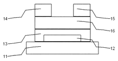
- FIG. 1 is a cross-sectional view illustrating one embodiment of an organic transistor according to the present invention.
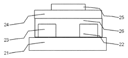
- FIG. 2 is a cross-sectional view illustrating one embodiment of the organic transistor according to the present invention.
- Reference numeral 11 denotes a substrate
- 12 denotes a gate electrode
- 13 denotes a gate insulating film
- 14 denotes a source electrode
- 15 denotes a drain electrode
- 16 denotes an organic semiconductor layer.
- Reference numeral 21 denotes a substrate
- 22 denotes a source electrode
- 23 denotes a drain electrode
- 24 denotes a gate insulating film
- 25 denotes a gate electrode
- 26 denotes an organic semiconductor layer.
- the present invention has the formula (1)
- the dichalcogenobenzodipyrrole compound (“compound (1)”) represented by these is provided.
- X and Y are each independently a sulfur atom, oxygen atom, selenium atom, tellurium atom or SO 2 Represents.
- the X and Y of the compound (1) are the same, the synthesis of the compound (1) is facilitated. Therefore, the X and Y of the compound (1) are preferably the same, and both are sulfur atoms. More preferred.
- R 1 ⁇ R 8 Each independently represents a hydrogen atom, a halogen atom, an alkyl group having 1 to 30 carbon atoms which may be substituted with a fluorine atom, an alkoxy group having 1 to 30 carbon atoms which may be substituted with a fluorine atom, fluorine An alkenyl group having 2 to 30 carbon atoms which may be substituted with an atom, an alkynyl group having 2 to 30 carbon atoms which may be substituted with a fluorine atom, or an alkyl group having 1 to 30 carbon atoms which may be substituted with a fluorine atom An alkylthio group, an aryl group having 6 to 30 carbon atoms, and a heteroaryl group having 4 to 30 carbon atoms are represented.
- the aryl group and the heteroaryl group are a fluorine atom, an alkyl group which may be substituted with a fluorine atom, an alkoxy group which may be substituted with a fluorine atom, an alkenyl group which may be substituted with a fluorine atom, fluorine It may have one or more selected from the group consisting of an alkynyl group optionally substituted with an atom and an alkylthio group optionally substituted with a fluorine atom.
- R 1 ⁇ R 4 Is preferably a halogen atom such as a fluorine atom or a hydrogen atom.
- the alkyl group having 1 to 30 carbon atoms may be linear, branched, or cyclic.
- R 1 ⁇ R 8 May be an alkyl group in which some or all of these hydrogen atoms are substituted with fluorine atoms.
- alkyl group examples include a methyl group, ethyl group, n-propyl group, n-butyl group, n-pentyl group, n-hexyl group, n-heptyl group, n-octyl group, n-nonyl group, n- Decyl group, n-undecyl group, n-dodecyl group, n-tridecyl group, n-tetradecyl group, n-pentadecyl group, n-hexadecyl group, n-heptadecyl group, n-octadecyl group, n-nonadecyl group, n- Icosyl group, n-henicosyl group, n-docosyl group, n-tricosyl group, n-tetracosyl group, n-pentacosyl group, n-hexacosyl
- alkyl group having 2 to 16 alkyl groups in which some or all of these hydrogen atoms are substituted with fluorine atoms is also preferable
- the alkoxy group having 1 to 30 carbon atoms may be linear, branched or cyclic.
- R 1 ⁇ R 8 May be an alkoxy group in which some or all of these hydrogen atoms are substituted with fluorine atoms.
- alkoxy groups include methoxy, ethoxy, n-propoxy, n-butoxy, n-pentyloxy, n-hexyloxy, n-heptyloxy, n-octyloxy, and n-decyloxy.
- n-undecyloxy group n-dodecyloxy group, n-tridecyloxy group, n-tetradecyloxy group, n-pentadecyloxy group, n-hexadecyloxy group, n-nonyloxy group, n- Heptadecyloxy group, n-octadecyloxy group, n-nonadecyloxy group, n-icosyloxy group, n-henicosyloxy group, n-docosyloxy group, n-tricosyloxy group, n-tetracosyloxy group, n -Pentacosyloxy group, n-hexacosyloxy group, n-heptacosyloxy group, n-octacosyloxy group, -Linear alkoxy group such as nonacosyloxy group, n-triacontyloxy group; isopropoxy group,
- ethoxy group, n-propoxy group, n-butoxy group, n-pentyloxy group, n-hexyloxy group, 2-ethylhexyloxy group, cyclohexyloxy group, n-heptyloxy group, n-octyloxy group, n-nonyloxy group, n-decyloxy group, 2-hexyldecyloxy group, n-undecyloxy group, n-dodecyloxy group, n-tridecyloxy group, n-tetradecyloxy group, n-pentadecyloxy group , N-hexadecyloxy group, methoxymethoxy group, methoxyethoxy group, methoxymethoxymethoxy group, alkoxy group having 1 to 16 carbon atoms of methoxyethoxyethoxy group, and part or all of these hydrogen atoms are fluor
- the alkenyl group in the present invention is an alkenyl group having 2 to 30 carbon atoms and may be linear, branched or cyclic. Also R 1 ⁇ R 8 And R 13 May be an alkenyl group in which some or all of these hydrogen atoms are substituted with fluorine atoms.
- alkenyl group examples include ethenyl group, 1-propenyl group, 1-butenyl group, 1-pentenyl group, 1-hexenyl group, 1-heptenyl group, 1-octenyl group, 1-nonenyl group, 1-decenyl group, 1-undecenyl group, 1-dodecenyl group, 1-tridecenyl group, 1-tetradecenyl group, 1-pentadecenyl group, 1-hexadecenyl group, 1-heptadecenyl group, 1-octadecenyl group, 1-nonadecenyl group, 1-icosenyl group, 1-henicosenyl group, 1-docosenyl group, 1-tricosenyl group, 1-tetracocenyl group, 1-pentacocenyl group, 1-hexacocenyl group, 1-heptacosenyl group, 1-oct
- ethenyl group Preferably ethenyl group, 1-propenyl group, 1-butenyl group, 1-pentenyl group, 1-hexenyl group, 1-heptenyl group, 1-octenyl group, 1-nonenyl group, 1-decenyl group, 1-undecenyl group, 2 carbon atoms such as 1-dodecenyl group, 1-tridecenyl group, 1-tetradecenyl group, 1-pentadecenyl group, 1-hexadecenyl group, 1-heptadecenyl group, 1-octadecenyl group, 1-nonadecenyl group, and 1-icosenyl group
- alkenyl groups of ⁇ 20 wherein some or all of these hydrogen atoms are replaced by fluorine atoms.
- ethenyl group More preferably ethenyl group, 1-propenyl group, 1-butenyl group, 1-pentenyl group, 1-hexenyl group, 1-heptenyl group, 1-octenyl group, 1-nonenyl group, 1-decenyl group, 1-undecenyl group , 1-dodecenyl group, 1-tridecenyl group, 1-tetradecenyl group, 1-pentadecenyl group, 1-hexadecenyl group and the like alkenyl groups having 2 to 16 carbon atoms, and some or all of these hydrogen atoms are fluorine atoms Those substituted with are also preferred.
- the alkynyl group having 2 to 30 carbon atoms in the present invention may be linear, branched or cyclic.
- R 1 ⁇ R 8 May be an alkynyl group in which some or all of these hydrogen atoms are substituted with fluorine atoms.
- alkynyl group examples include ethynyl group, 1-propynyl group, 1-butynyl group, 1-pentynyl group, 1-hexynyl group, 1-heptynyl group, 1-octynyl group, 1-noninyl group, 1-decynyl group, 1-undecyl group, 1-dodecynyl group, 1-tridecynyl group, 1-tetradecynyl group, 1-pentadecynyl group, 1-hexadecynyl group, 1-heptadecynyl group, 1-octadecynyl group, 1-nonadecynyl group, 1-icosinyl group, 1-henicosinyl group, 1-docosinyl group, 1-tricosinyl group, 1-tetracosinyl group, 1-pentacosynyl group, 1-hexacosinyl
- ethynyl group Preferably ethynyl group, 1-propynyl group, 1-butynyl group, 1-pentynyl group, 1-hexynyl group, 1-heptynyl group, 1-octynyl group, 1-noninyl group, 1-decynyl group, 1-undecynyl group, 2 carbon atoms such as 1-dodecynyl group, 1-tridecynyl group, 1-tetradecynyl group, 1-pentadecynyl group, 1-hexadecynyl group, 1-heptadecynyl group, 1-octadecynyl group, 1-nonadecynyl group and 1-icosinyl group
- a ⁇ 20 alkynyl group in which some or all of these hydrogen atoms are substituted with fluorine atoms is also preferred.
- the alkylthio group having 1 to 30 carbon atoms in the present invention may be linear, branched or cyclic.
- R 1 ⁇ R 8 May be an alkylthio group in which some or all of these hydrogen atoms are substituted with fluorine atoms.
- the alkylthio group include methylthio group, ethylthio group, n-propylthio group, isopropylthio group, n-butylthio group, n-pentylthio group, n-hexylthio group, n-heptylthio group, n-octylthio group, and n-nonylthio group.
- n-decylthio group n-undecylthio group, n-dodecylthio group, n-tridecylthio group, n-tetradecylthio group, n-pentadecylthio group, n-hexadecylthio group, n-heptadecylthio group, n-octadecylthio group Group, n-nonadecylthio group, n-icosylthio group, n-henicosylthio group, n-docosylthio group, n-tricosylthio group, n-tetracosylthio group, n-pentacosylthio group, n-hexacosylthio group, n- Heptacosylthio group, n-octacosylthio group, n-nonacosylthio Linear alkylthio
- R 1 ⁇ R 8 May be an aryl group in which some or all of the hydrogen atoms are substituted with fluorine atoms.
- R 1 ⁇ R 8 Is a group consisting of an alkyl group substituted with a fluorine atom, an alkoxy group substituted with a fluorine atom, an alkenyl group substituted with a fluorine atom, an alkynyl group substituted with a fluorine atom, and an alkylthio group substituted with a fluorine atom. It may be an aryl group having one or more selected.
- the alkyl group, the alkoxy group, the alkenyl group, the alkynyl group and the alkylthio group are as described above.
- the aryl group having a substituent preferably has 7 to 30 carbon atoms in total including the substituent.
- R 1 ⁇ R 8 A preferred example of is an aryl group having an alkyl group or an alkoxy group.
- Preferred examples include methylphenyl group, ethylphenyl group, n-propylphenyl group, isopropylphenyl group, n-butylphenyl group, n-pentylphenyl group, n-hexylphenyl group, n-heptylphenyl group, n-octyl.
- Straight chain having 1 to 24 carbon atoms such as phenyl group, n-nonylphenyl group, n-decylphenyl group, n-undecylphenyl group, n-dodecylphenyl group, n-tridecylphenyl group and n-tetradecylphenyl group; Phenyl group having a chain alkyl group; methoxyphenyl group, ethoxyphenyl group, n-propoxyphenyl group, n-butoxyphenyl group, n-pentyloxyphenyl group, n-hexyloxyphenyl group, n-heptyloxyphenyl group, n -Octyloxyphenyl group, n-decyloxyphenyl group, n- Examples thereof include a phenyl group having a linear alkoxy group having 1 to 24 carbon atoms such as an undecyloxyphenyl
- the heteroaryl group having 4 to 30 carbon atoms in the present invention is, for example, a thiophenylyl group, a furanyl group, a selenophenyl group, a pyrrolyl group, an oxazolyl group, a thiazole group, a pyridinyl group, a pyrazinyl group, a pyrimidinyl group, or a pyridazinyl group.
- R 1 ⁇ R 8 May be a heteroaryl group in which some or all of the hydrogen atoms are substituted with fluorine atoms.
- R 1 ⁇ R 8 Is a group consisting of an alkyl group substituted with a fluorine atom, an alkoxy group substituted with a fluorine atom, an alkenyl group substituted with a fluorine atom, an alkynyl group substituted with a fluorine atom, and an alkylthio group substituted with a fluorine atom. It may be a heteroaryl group having one or more selected.
- the alkyl group, the alkoxy group, the alkenyl group, the alkynyl group and the alkylthio group are as described above.
- the carbon number of the heteroaryl group having a substituent is preferably 7 to 16 in total including the substituent.
- the halogen atom is a fluorine atom, a chlorine atom, a bromine atom or an iodine atom, and R 1 ⁇ R 8
- the halogen atom is preferably a fluorine atom.
- R 1 And R 2 Are preferably the same.
- R 1 And R 2 Is preferably a halogen atom such as a hydrogen atom or a fluorine atom.
- R 3 And R 4 Are preferably the same.
- R 1 And R 2 Is preferably a halogen atom such as a hydrogen atom or a fluorine atom.
- R 1 ⁇ R 4 Those in which all are hydrogen atoms are preferred.
- R 5 And R 6 are preferably hydrogen atoms.
- R 7 And R 8 are the same and R 7 And R 8 Is preferably an aryl group having 7 to 26 carbon atoms, which may have an alkyl group substituted with a fluorine atom.
- Preferred R 7 And R 8 Specific examples are methylphenyl group, ethylphenyl group, n-propylphenyl group, isopropylphenyl group, n-butylphenyl group, n-pentylphenyl group, n-hexylphenyl group, n-heptylphenyl group, n-octyl.
- Straight chain having 1 to 14 carbon atoms such as phenyl group, n-nonylphenyl group, n-decylphenyl group, n-undecylphenyl group, n-dodecylphenyl group, n-tridecylphenyl group and n-tetradecylphenyl group; Phenyl group having a chain alkyl group; for example, methoxyphenyl group, ethoxyphenyl group, n-propoxyphenyl group, n-butoxyphenyl group, n-pentyloxyphenyl group, n-hexyloxyphenyl group, n-heptyloxyphenyl group N-octyloxyphenyl group, n-decyloxyphenyl group, n- A ndecyloxyphenyl group, an n-dodecyloxyphenyl group, an n-tridecy
- R 7 And R 8 are identical and R 7 And R 8 Is preferably an alkyl group having 1 to 20 carbon atoms which may be substituted with a fluorine atom.
- R 7 And R 8 Specific examples are methyl group, ethyl group, n-propyl group, isopropyl group, n-butyl group, s-butyl group, t-butyl group, n-pentyl group, neopentyl group, n-hexyl group, 2-ethylhexyl.
- Examples of compound (1) are listed in Tables 1-8. In Tables 1 to 8, the wavy line represents a bond.
- Preferred compounds (1) are represented by the compound numbers shown in the table, for example, (1-1-1), (1-1-2), (1-1-3), (1-1- 4), (1-1-5), (1-1-6), (1-1-8), (1-1-9), (1-1-11), (1-1-12) , (1-1-13), (1-1-14), (1-1-15), (1-1-19), (1-1-21), (1-1-22), ( 1-1-24), (1-1-25), (1-1-26), (1-1-28), (1-1-29), (1-1-30), (1- 1-31), (1-1-33), (1-1-35), (1-1-42), (1-1-45), (1-1-51), (1-1- 52), (1-1-56), (1-1-58), (1-1-59), (1-1-61), (1-1-64), ( -1-65), (1-1-67), (1-1-68), (1-2-2), (1-2-7), (
- the compound (1) of the present invention can form a thin film by a vacuum process. Moreover, since the compound (1) is excellent in solubility in an organic solvent, a thin film can be formed by a solution process.
- the soluble organic solvent include alcohol solvents such as water, methanol, ethanol, isopropyl alcohol, and butanol, and aromatics such as benzene, toluene, xylene, chlorobenzene, o-dichlorobenzene, trichlorobenzene, and fluorobenzene.
- Hydrocarbon solvents such as dichloromethane, chloroform, 1,2-dichloroethane, 1,1 ′, 2,2′-tetrachloroethane, tetrachloroethylene, carbon tetrachloride and the like halogenated aliphatic hydrocarbon solvents such as diethyl ether, dioxane, tetrahydrofuran Ether solvents such as anisole, aliphatic hydrocarbon solvents such as pentane, hexane, pentane, octane and cyclohexane, keto such as acetone, methyl ethyl ketone, methyl isobutyl ketone and cyclohexanone Solvents, ester solvents such as ethyl acetate and butyl acetate, nitrile solvents such as acetonitrile, propionitrile, methoxyacetonitrile, glutarodinitrile and benzonitrile,
- the concentration of the compound (1) in the organic solution containing the compound (1) is usually within the range of 0.001 to 50% by weight, preferably 0.01 to 10% by weight, more preferably 0.1 to 5%. Within the weight percent range.
- an antioxidant, a stabilizer, an organic semiconductor material, an organic insulating material, and the like are contained in an amount that does not significantly impair the carrier mobility of a thin film that is an organic semiconductor layer described later. It may be contained.
- the organic semiconductor material may be a low-molecular material or a high-molecular material, and may be crosslinked or not crosslinked when a crosslinking reaction is possible.
- a polymer material is used.
- the content of the compound (1) is preferably 10% by weight or more, and more preferably adjusted to 20% by weight or more.
- the organic insulating material may be a low-molecular material or a high-molecular material, and may be crosslinked or not crosslinked when a crosslinking reaction is possible.
- a polymer material is used.
- Specific examples include polystyrene, polycarbonate, polydimethylsiloxane, nylon, polyimide, cyclic olefin copolymer, epoxy polymer, cellulose, polyoxymethylene, polyolefin polymer, polyvinyl polymer, polyester polymer, polyether polymer, polyamide polymer. , Fluoropolymers, biodegradable plastics, phenolic resins, amino resins, unsaturated polyester resins, diallyl phthalate resins, epoxy resins, polyimide resins, polyurethane resins, silicone resins, and copolymers combining various polymer units.
- the content of the compound (1) is preferably 10% by weight or more, and more preferably 20% by weight or more.
- the organic solution can be prepared by dissolving the compound (1) in an organic solvent, for example, in the range of 10 to 200 ° C., preferably in the range of 20 to 150 ° C.
- the compound (1) of the present invention is represented, for example, by the formula (2) (Wherein R 1 ⁇ R 6 , X and Y are as defined above, R 9 ⁇ R 12 Each independently represents a halogen atom, preferably bromine or iodine.
- the aryl group and the heteroaryl group are a fluorine atom, an alkyl group which may be substituted with a fluorine atom, an alkoxy group which may be substituted with a fluorine atom, an alkenyl group which may be substituted with a fluorine atom, fluorine It may have an alkynyl group which may be substituted with an atom or an alkylthio group which may be substituted with a fluorine atom. ) It can manufacture by making the amine compound shown by react.
- R 7 I a hydrogen atom, a halogen atom, an alkyl group having 1 to 30 carbon atoms that may be substituted with a fluorine atom, an alkoxy group having 1 to 30 carbon atoms that may be substituted with a fluorine atom, or a fluorine atom.
- An alkenyl group having 2 to 30 carbon atoms, an alkynyl group having 2 to 30 carbon atoms which may be substituted with a fluorine atom, an alkylthio group having 1 to 30 carbon atoms which may be substituted with a fluorine atom, 6 carbon atoms Represents a 30 to 30 aryl group or a C 4 to 30 heteroaryl group;
- the aryl group and the heteroaryl group are a fluorine atom, an alkyl group which may be substituted with a fluorine atom, an alkoxy group which may be substituted with a fluorine atom, an alkenyl group which may be substituted with a fluorine atom, fluorine It may have an alkynyl group which may be substituted with an atom or an alkylthio group which may be substituted with a fluorine atom.
- the dichalcogenobenzodipyrrole compound represented by the above formula (1 ') is produced.
- Examples of the compound (2) used for the production of the compound (1) include the compounds shown in the following table. In Tables 9 to 14, the wavy line represents a bond.
- Examples of the amine compound used in the reaction include methylamine, ethylamine, n-propylamine, isopropylamine, n-butylamine, n-pentylamine, n-hexylamine, n-heptylamine, n-octylamine, n- Nonylamine, n-decylamine, n-undecylamine, n-dodecylamine, n-tridecylamine, n-tetradecylamine, n-pentadecylamine, n-hexadecylamine, n-heptadecylamine, n-octadecylamine Amine, n-nonadecylamine, n-icosylamine, n-henicosylamine, n-docosylamine, n-tricosylamine, n-tetracosylamine, n-penta
- the amount of the amine compound used for the reaction is usually 1 to 50 mol, preferably 2 to 20 mol, more preferably 2 to 15 mol, per 1 mol of compound (2).
- the reaction is preferably performed in an organic solvent.
- the organic solvent is not particularly limited as long as it is inert to the above reaction, and examples thereof include aromatic hydrocarbon solvents such as toluene and xylene; halogen atomized aromatic hydrocarbon solvents such as chlorobenzene and o-dichlorobenzene.
- Aliphatic hydrocarbon solvents such as hexane, heptane and dimethoxyethane; halogenated aliphatic hydrocarbon solvents such as chloroform and 1,2-dichloroethane; carbon atoms of 1 to 4 such as methanol, isopropyl alcohol and t-butyl alcohol; Alcohols; ether solvents such as tetrahydrofuran and dioxane; mixed solvents thereof can be mentioned, preferably aromatic hydrocarbon solvents and aliphatic hydrocarbon solvents, more preferably toluene and xylene.
- the concentration of the compound (2) in the reaction solution is, for example, 0.0001 to 20 mol, preferably 0.001 to 10 mol, more preferably 0.01 to 5 mol per liter of the organic solvent.
- the reaction is preferably performed in the presence of a palladium catalyst and a base.
- the amount of the palladium catalyst used is usually 0.01 to 50 mol, preferably 0.01 to 30 mol in terms of palladium atom, per 100 mol of the compound (2).
- the palladium catalyst may be prepared by previously bringing a ligand compound and a palladium compound into contact with each other in an organic solvent, or contacting a ligand compound and a palladium compound in a reaction system. You may use what was prepared.
- a monodentate phosphine type ligand As a compound which becomes said ligand, what is necessary is just to be able to coordinate to palladium and to be soluble in an organic solvent, for example, a monodentate phosphine type ligand, a polydentate ligand, a carbene type ligand etc.
- a monodentate ligand is preferable, and a monodentate phosphine-based ligand is more preferable.
- Examples of monodentate phosphine-based ligands include tri (n-butyl) phosphine, tri (t-butyl) phosphine, tricyclohexylphosphine, triphenylphosphine, tri (o-tolyl) phosphine, trinaphthylphosphine, and diphenylnaphthylphosphine. And dicyclohexylnaphthylphosphine, and tri (t-butyl) phosphine is preferable.
- bidentate ligand examples include 2,2′-bis (diphenylphosphino) -1,1′-binaphthyl, 1,2-bis (diphenylphosphino) ethane, and 1,3-bis (diphenylphosphino).
- a commercially available product may be used as it is, or a ligand produced by a known method may be used.
- the amount of the ligand used is preferably 0.5 to 20 moles per mole of palladium atoms of the palladium compound.
- the palladium compound examples include palladium acetate, palladium chloride, dichlorobis (acetonitrile) palladium, palladium acetylacetonate, dichloro (cycloocta-1,5-diene) palladium, dibromobis (benzonitrile) palladium, di- ⁇ -chlorobis ( ⁇ - Divalent palladium compounds such as allyl) dipalladium, dichlorobis (pyridine) palladium, dichlorobis (triphenylphosphine) palladium, dichloro- [1,1′-bis (diphenylphosphino) ferrocene] palladium / dichloromethane complex; Zero-valent palladium compounds such as benzylideneacetone) dipalladium, tris (dibenzylideneacetone) dipalladium / chloroform complex, tetrakis (triphenylphosphine) palladium; Among them, tris (d
- the palladium compound a commercially available product may be used as it is, or a product produced by a known method may be used.
- the base include alkaline earth metal hydroxides such as calcium hydroxide; alkaline metal carbonates such as potassium carbonate, sodium carbonate and cesium carbonate; alkaline earth metal carbonates such as magnesium carbonate, calcium carbonate and barium carbonate
- Alkali metal phosphates such as lithium phosphate, potassium phosphate, sodium phosphate; sodium methoxide, sodium ethoxide, sodium t-butoxide, potassium methoxide, potassium ethoxide, potassium t-butoxide, lithium t-butoxide
- Alkali metal carbonates and alkali metal alkoxides are preferable, alkali metal alkoxides are more preferable, and alkali metal alkoxides having 1 to 6 carbon atoms are more preferable.
- a base may be used independently and may mix and use two or more types.
- the amount of the base used is, for example, 0.1 to 25 mol, preferably 1 to 20 mol, more preferably 2 to 10 mol, per 1 mol of compound (2). It is preferable for the amount of base used to be 25 mol or less because the proportion of unreacted amine compound (3) tends to be reduced.
- the reaction temperature is selected from the range of 0 ° C. to the reflux temperature of the reaction solution, but is preferably in the range of 40 to 200 ° C.
- the reaction time is usually in the range of 1 minute to 120 hours. When stopping the reaction, for example, water or dilute hydrochloric acid is added to the reaction solution.
- a crude product of compound (1) can be obtained by performing post-treatment operations such as extraction and washing.
- the crude product can be purified by performing a purification operation such as crystallization, sublimation, or various chromatographies or a combination of these.
- the general formula (4) (Wherein R 5 And R 6 Is the same definition as above.
- R 14 ⁇ R 17 Each represents a halogen atom.
- a compound represented by the formula (compound (4)) and General formula (5) In the formula, X has the same definition as above.
- R 18 And R 19 Each represents a halogen atom.
- the thin film of the present invention is a thin film containing the compound (1), for example, a thin film having a thickness of 1 nm to 10 ⁇ m, preferably a thickness of 5 nm to 1 ⁇ m.
- the thin film of the present invention may exhibit luminescent properties and conductivity similar to semiconductors, and is excellent as a luminescent thin film and a conductive thin film, respectively.
- the luminescent thin film means a thin film containing the compound (1) and emits light under conditions of light or electrical stimulation.
- the light-emitting thin film is useful as a material for a light-emitting element.
- a light-emitting element having a light-emitting thin film is also one aspect of the present invention.
- the light-emitting device of the present invention is useful as a material for organic light-emitting diodes, for example.
- the light emitting element means a device using the light emitting thin film.
- the conductive thin film means a thin film that exhibits conductivity under the condition of light or electrical stimulation.
- a conductive thin film showing conductivity similar to that of a semiconductor is sometimes referred to as an organic semiconductor thin film.
- the conductive thin film is useful as a material for an organic semiconductor device described later.
- the conductive thin film and the luminescent thin film of the present invention can be produced in the same manner as a conventionally known method except that the compound (1) of the present invention is used as a material.
- the organic transistor will be described.
- the organic transistor of the present invention includes the thin film of the present invention. Since the organic transistor contains the compound (1) of the present invention, it has high carrier mobility.
- the organic transistor has a carrier mobility of 10 -6 cm 2 / Vs or more.
- the carrier mobility can be measured by applying the following formula (a) to the drain current and the gate voltage measured using a parameter analyzer or the like.
- the organic transistor of the present invention includes an organic field effect transistor.
- the source electrode and the drain electrode are usually in contact with the semiconductor layer, and a gate electrode may be provided with an insulating layer (dielectric layer) in contact with the active layer interposed therebetween.
- the element structure of the organic transistor is, for example, (1) Structure comprising substrate / gate electrode / insulator layer / source electrode / drain electrode / semiconductor layer; (2) Structure composed of substrate / gate electrode / insulator layer / semiconductor layer / source electrode / drain electrode (see FIG. 1); (3) Structure composed of substrate / semiconductor layer + source electrode / drain electrode / insulator layer / gate electrode (see FIG. 2); (4) Structure consisting of substrate / source electrode (or drain electrode) / semiconductor layer + insulator layer + gate electrode / drain electrode (or source electrode), Is mentioned.
- the semiconductor layer has the organic semiconductor thin film of the present invention.
- each structure In the case where there are a plurality of the semiconductor layers in each structure, they may be provided in the same plane or stacked. In each of the above structures, a plurality of source electrodes, drain electrodes, and gate electrodes may be provided.
- Examples of a method for forming an organic semiconductor layer containing the compound (1) as a thin film in an organic transistor include a formation method in a vacuum process such as a vacuum deposition method, a sputtering method, a CVD method, and a molecular beam epitaxial growth method.
- a vacuum deposition method is used.
- the vacuum deposition method is a method in which an organic semiconductor material such as compound (1) is heated in a crucible or a metal boat under vacuum, and the evaporated organic semiconductor material is deposited on a substrate or an insulator material.
- Degree of vacuum during deposition is 1 ⁇ 10 -1 Pa or less, preferably 1 ⁇ 10 -3 Pa or less.
- the substrate temperature during vapor deposition is 0 ° C. to 300 ° C., preferably 20 ° C. to 200 ° C.
- the deposition rate is 0.001 nm / sec to 10 nm / sec, preferably 0.01 nm / sec to 1 nm / sec.
- the film thickness of the organic semiconductor thin film is 1 nm to 10 ⁇ m, preferably 5 nm to 1 ⁇ m.
- Different embodiments of the method for forming the organic semiconductor layer containing the compound (1) as a thin film in the organic transistor exemplifies the coating film forming process because the compound (1) is excellent in solubility in an organic solvent. be able to.
- a solution-like composition obtained by dissolving the compound (1) in an organic solvent is usually prepared, and the composition is applied to a substrate or an insulator layer, and applied onto the substrate. A step of drying the applied coating film.
- Examples of the coating process include a casting method, a dip coating method, a die coater method, a roll coater method, a bar coater method, a spin coating method, an inkjet method, a screen printing method, an offset printing method, and a micro contact printing method. Etc. These steps may be used alone or in combination of two or more.
- the coating film obtained by the coating step is dried, that is, the organic solvent contained in the composition is removed, whereby the thin film of the present invention can be obtained.
- Examples of the drying method include natural drying treatment, heat treatment, reduced pressure treatment, ventilation treatment, or a combination of these, and natural drying treatment or heat treatment is preferable in terms of simple operation.
- Specific examples include a treatment in which the substrate is left in the atmosphere or heated on a hot plate (for example, 40 to 250 ° C., preferably 50 to 200 ° C.).
- the compound (1) may not be dissolved in the organic solvent, but the compound (1) may be dispersed in the solvent.
- a specific embodiment in this case means that the composition described above is a dispersion in which compound (1) is dispersed in a solvent.
- a coating film forming process using a composition obtained by dissolving the compound (1) with an organic solvent is preferable. An organic transistor obtained from such a thin film exhibits excellent carrier mobility.
- the material constituting the source electrode, the drain electrode, and the gate electrode is not particularly limited as long as it is a general conductive material.
- a known conductive polymer whose conductivity is improved by doping or the like for example, conductive polyaniline, conductive polypyrrole, conductive polythiophene, a complex of polyethylenedioxythiophene and polystyrenesulfonic acid, or the like is also preferably used. Among them, those having low electrical resistance at the contact surface with the semiconductor layer are preferable.
- These electrode materials may be used alone or in combination of two or more. Although the film thickness of the electrode varies depending on the material, it may be 0.1 nm to 10 ⁇ m, preferably 0.5 nm to 5 ⁇ m, more preferably 1 nm to 3 ⁇ m.
- the electrode film when it serves as a gate electrode and a board
- Various methods can be used as a patterning method. Specifically, a photolithographic method combining photoresist patterning and etching may be used.
- printing methods such as ink jet printing, screen printing, offset printing, letterpress printing, and soft lithography techniques such as a microcontact printing method are also included.
- Inorganic oxides include silicon oxide, aluminum oxide, tantalum oxide, titanium oxide, tin oxide, vanadium oxide, barium strontium titanate, barium zirconate titanate, lead zirconate titanate, lead lanthanum titanate, strontium titanate, Barium titanate, barium magnesium fluoride, bismuth titanate, strontium bismuth titanate, strontium bismuth tantalate, bismuth tantalate niobate, trioxide yttrium, etc.
- silicon oxide aluminum oxide, tantalum oxide, Titanium oxide.
- examples thereof include inorganic nitrides such as silicon nitride and aluminum nitride.
- organic compound film polystyrene, polyimide, polyamide, polyester, polyacrylate, photo radical polymerization system, photo cation polymerization system photo-curing resin, copolymer containing acrylonitrile component, polyvinyl phenol, polyvinyl alcohol, novolac resin
- examples include cyanoethyl pullulan, and preferably polystyrene, polyimide, polyvinylphenol, and polyvinyl alcohol.
- the thickness of the insulating layer varies depending on the material, but is usually from 0.1 nm to 100 ⁇ m, preferably from 0.5 nm to 50 ⁇ m, more preferably from 5 nm to 10 ⁇ m.
- various known methods can be used. Specifically, spin coating, spray coating, dip coating, casting, bar coating, blade coating and other coating methods, screen printing, offset printing, inkjet printing methods, vacuum deposition, molecular beam epitaxial growth, ion cluster beam And dry process methods such as ion plating, sputtering, atmospheric pressure plasma, and CVD.
- a sol-gel method alumite on aluminum, and a method of forming an oxide film on a metal such as a thermal oxide film of silicon.
- the substrate include a plate or sheet made of glass, paper, quartz, ceramic, or a flexible resin substrate material.
- the resin film include polyethylene terephthalate (PET), polyethylene naphthalate (PEN), polyethersulfone (PES), polyetherimide, polyetheretherketone, polyphenylene sulfide, polyarylate, polyimide, polycarbonate (PC ), Cellulose triacetate (TAC), cellulose acetate propionate (CAP), and the like.
- the thickness of the substrate is preferably 1 ⁇ m to 10 mm, more preferably 5 ⁇ m to 5 mm.
- surface treatment may be performed on the insulator layer or substrate.
- the surface treatment includes hydrophobization treatment with hexamethyldisilazane, octadecyltrichlorosilane, octyltrichlorosilane, phenethyltrichlorosilane, acid treatment with hydrochloric acid, sulfuric acid, hydrogen peroxide water, sodium hydroxide, water, etc.
- the surface treatment method include a vacuum deposition method, a sputtering method, a coating method, a printing method, and a sol-gel method.
- a protective film made of a resin or an inorganic compound may be provided on the semiconductor layer.
- the organic transistor of the present invention can be used for organic semiconductor devices such as liquid crystal display elements, organic electroluminescent elements, electronic paper, sensors, RFIDs (radio frequency identification cards), and the like.
- the starting material 1,4-dibromo-2,5-diiodobenzene was prepared by reacting 1,4-dibromobenzene with iodine (see J. Org. Chem., 1985, page 3104).
- 2,3-dibromothiophene manufactured by Tokyo Chemical Industry, 22.3 g, 92.3 mmol
- the solution was cooled to ⁇ 78 ° C., and a tetrahydrofuran solution (92.3 ml, 92.3 mmol) containing isopropylmagnesium bromide (manufactured by Tokyo Chemical Industry, 1.00 M) was added at the same temperature from the dropping funnel over 1 hour. For 30 minutes.
- a diethyl ether solution (92.3 ml, 92.3 mmol) containing zinc chloride (manufactured by Aldrich, 1.00 M) was added to the solution at ⁇ 78 ° C. through a dropping funnel over 1 hour, and the mixture was stirred at the same temperature for 10 minutes. After the temperature of the solution was gradually raised to room temperature, the solvent was distilled off under reduced pressure to obtain white crystals.
- 1,4-Dibromo-2,5-diiodobenzene (15.0 g, 30.8 mmol) and tetrakistriphenylphosphine (manufactured by Tokyo Chemical Industry, 3.5 g, 3.1 mmol) were charged into this crystal, and the system was filled with nitrogen. After replacement, 240 ml of dehydrated tetrahydrofuran was added by syringe, and the mixture was stirred for 7 hours under reflux. The solution was cooled to room temperature and the solvent was removed under reduced pressure.
- a 10% aqueous ammonium chloride solution (weight ratio) and toluene were added to the concentrated residue and the phases were separated, and the resulting toluene layer was dried over magnesium sulfate and filtered, and then the solvent was distilled off under reduced pressure. Hexane was added to the resulting mixture and the mixture was refluxed for 10 minutes, cooled to room temperature, the mixture was filtered, and the filtered product was dried under reduced pressure.
- Example 1 Production Example of Compound (1-1-26)
- Compound (2-2-1) 10.00 g (17.92 mmol), tris (dibenzylideneacetone) dipalladium (3.28 g, 3.69 mmol), in a 500 mL four-necked flask equipped with a stirrer, a thermometer, and a condenser, Tri-tert-butylphosphine (1.45 g, 7.17 mmol), p-dodecylaniline (18.74 g, 71.69 mmol), sodium tert-butoxide (10.33 g, 107.54 mmol) and 300 ml of dehydrated toluene in a nitrogen atmosphere Then, the mixture was heated up to 80 ° C.
- the obtained crystals were further purified by recycle preparative high performance liquid chromatography (mobile bed; tetrahydrofuran, acetonitrile mixed solvent) to give white yellow crystals of compound (1-1-14) (0.67 g, 1.11 mmol). Was obtained in a yield of 12%.
- the physical properties of the compound (1-1-14) were as follows.
- the thickness of the chromium layer was 5 nm, and the thickness of the gold layer was 40 nm.
- the substrate was subjected to ultrasonic cleaning in the order of acetone and isopropyl alcohol, dried, cleaned with oxygen plasma, and then heated at 80 ° C. for 5 minutes for dehydration operation.
- the channel width was 2 mm, and the channel length was 100 ⁇ m.
- the channel portion was treated with phenethyltrichlorosilane and the electrode portion was treated with pentafluorobenzenethiol. Then, in a nitrogen atmosphere, 0.4 wt% o- of the compound (1-1-26) produced in Example 1 was used.
- a xylene solution was dropped, an organic layer was dropped by a spin coating method, and then a solution containing a fluorine-based polymer was dropped on the organic layer to form an insulating layer by a spin coating method.
- the film thickness of the compound (1-1-26) at this time was 25 nm, and the film thickness of the insulating layer was 300 nm.
- chromium and aluminum were vapor-deposited in this order, and a gate electrode was installed to obtain an organic transistor as shown in FIG. At this time, the thickness of the chromium layer was 5 nm, and the thickness of the aluminum layer was 200 nm. Next, the electrical characteristics of the obtained organic transistor were measured.
- the organic transistor having a thin film of the compound (1-1-26) in the organic semiconductor layer was a p-type organic transistor.
- L and W are the gate length and gate width of the organic transistor
- Ci is the capacitance per unit area of the gate insulating film
- Vg is the gate voltage
- Vt is the gate voltage. It is a threshold voltage.
- the carrier mobility was 0.25 (cm 2 / V ⁇ s).
- the present invention provides an organic semiconductor device having high carrier mobility, a thin film contained in the device, and a compound contained in the thin film.
Landscapes
- Chemical & Material Sciences (AREA)
- Organic Chemistry (AREA)
- Engineering & Computer Science (AREA)
- Physics & Mathematics (AREA)
- Spectroscopy & Molecular Physics (AREA)
- Materials Engineering (AREA)
- Manufacturing & Machinery (AREA)
- Thin Film Transistor (AREA)
- Electroluminescent Light Sources (AREA)
- Heterocyclic Carbon Compounds Containing A Hetero Ring Having Oxygen Or Sulfur (AREA)
- Liquid Deposition Of Substances Of Which Semiconductor Devices Are Composed (AREA)
- Physical Deposition Of Substances That Are Components Of Semiconductor Devices (AREA)
Abstract
式(1)(式中、X及びYは、それぞれ独立して、硫黄原子、酸素原子、セレン原子、テルル原子、及びSO2を表す。R1~R8は、それぞれ独立して、水素原子、ハロゲン原子、炭素数1~30のアルキル基、炭素数1~30のアルコキシ基、炭素数2~30のアルケニル基、炭素数2~30のアルキニル基、炭素数1~30のアルキルチオ基、炭素数6~30のアリール基又は炭素数4~30のヘテロアリール基等を表す。)で表されるジカルコゲノベンゾジピロール化合物は、キャリア移動度の高い有機半導体デバイスに利用できる。
Description
本発明はジカルコゲノベンゾジピロール化合物、該化合物の製造方法、該化合物を含む薄膜及び該薄膜を含む有機半導体デバイス等に関する。
有機化合物を有機溶媒に溶解し、得られる溶液状の組成物を電極などに塗布し、該組成物中の有機溶媒を乾燥して薄膜を得、該薄膜を含む有機トランジスタなどの有機半導体デバイスは、キャリア移動度などの半導体特性を有する場合があることが知られている。例えば、特開2009−99658号公報の実施例14には、下記式
 で表される化合物をクロロベンゼンに溶解した溶液をゲート電極上に塗布し、クロロベンゼンを乾燥して薄膜を得ること、該薄膜を含む有機トランジスタは、7.4×10⁻²(cm2/V・s)のキャリア移動度を有することが記載されている。
しかし、キャリア移動度がさらに向上した有機半導体デバイスが求められていた。
しかし、キャリア移動度がさらに向上した有機半導体デバイスが求められていた。
本発明は、以下のものである。
<1> 式(1)
 (式中、X及びYは、それぞれ独立して、硫黄原子、酸素原子、セレン原子、テルル原子又はSO2を表す。R1~R8は、それぞれ独立して、水素原子、ハロゲン原子、フッ素原子で置換されていてもよい炭素数1~30のアルキル基、フッ素原子で置換されていてもよい炭素数1~30のアルコキシ基、フッ素原子で置換されていてもよい炭素数2~30のアルケニル基、フッ素原子で置換されていてもよい炭素数2~30のアルキニル基、フッ素原子で置換されていてもよい炭素数1~30のアルキルチオ基、炭素数6~30のアリール基又は炭素数4~30のヘテロアリール基を表す。該アリール基及び該ヘテロアリール基は、フッ素原子、フッ素原子で置換されていてもよいアルキル基、フッ素原子で置換されていてもよいアルコキシ基、フッ素原子で置換されていてもよいアルケニル基、フッ素原子で置換されていてもよいアルキニル基及びフッ素原子で置換されていてもよいアルキルチオ基からなる群より選ばれる一以上を有していてもよい。)
で表されるジカルコゲノベンゾジピロール化合物。
<2> 前記式(1)において、X及びYが硫黄原子である<1>に記載のジカルコゲノベンゾジピロール化合物。
<3> 前記式(1)において、R3及びR4が、水素原子又はハロゲン原子であり、R7及びR8が、炭素数1~30のアルキル基、炭素数7~30のアリール基又は炭素数5~30のヘテロアリール基(該アリール基及び該ヘテロアリール基はフッ素原子で置換されていてもよいアルキル基又はフッ素原子で置換されていてもよいアルコキシ基を有する。)である<1>又は<2>に記載のジカルコゲノベンゾジピロール化合物。
<4> 前記式(1)において、R5及びR6が水素原子である<1>~<3>のいずれかに記載のジカルコゲノベンゾジピロール化合物。
<5> 前記式(1)において、R1~R4は、水素原子又はハロゲン原子である<1>~<4>のいずれかに記載のジカルコゲノベンゾジピロール化合物。
<6> 前記式(1)において、R7及びR8がフッ素原子で置換されていてもよいアルキル基を有する炭素数7~26のアリール基である<1>~<5>のいずれかに記載のジカルコゲノベンゾジピロール化合物。
<7> 前記式(1)において、R7及びR8がフッ素原子で置換されていてもよい炭素数1~20のアルキル基である<1>~<6>のいずれかに記載のジカルコゲノベンゾジピロール化合物。
<8> <1>~<7>のいずれかに記載のジカルコゲノベンゾジピロール化合物を含む薄膜。
<9> <1>~<7>のいずれかに記載のジカルコゲノベンゾジピロール化合物からなる薄膜。
<10> <8>又は<9>に記載の薄膜を含む有機トランジスタ。
<11> <8>又は<9>に記載の薄膜を含む有機半導体デバイス。
<12> 式(2)
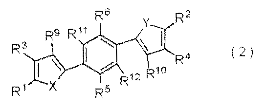 (式中、X及びYは、それぞれ独立して、硫黄原子、酸素原子、セレン原子、テルル原子又はSO2を表す。R1~R6は、それぞれ独立して、水素原子、ハロゲン原子、フッ素原子で置換されていてもよい炭素数1~30のアルキル基、フッ素原子で置換されていてもよい炭素数1~30のアルコキシ基、フッ素原子で置換されていてもよい炭素数2~30のアルケニル基、フッ素原子で置換されていてもよい炭素数2~30のアルキニル基、フッ素原子で置換されていてもよい炭素数1~30のアルキルチオ基、炭素数6~30のアリール基又は炭素数4~30のヘテロアリール基を表す。該アリール基及び該ヘテロアリール基は、フッ素原子、フッ素原子で置換されていてもよいアルキル基、フッ素原子で置換されていてもよいアルコキシ基、フッ素原子で置換されていてもよいアルケニル基、フッ素原子で置換されていてもよいアルキニル基及びフッ素原子で置換されていてもよいアルキルチオ基からなる群より選ばれる一以上を有していてもよい。R9~R12は、それぞれ独立して、ハロゲン原子を表す。)
と、式(3)
R7−NH2 (3)
(式中、R7は水素原子、ハロゲン原子、フッ素原子で置換されていてもよい炭素数1~30のアルキル基、フッ素原子で置換されていてもよい炭素数1~30のアルコキシ基、フッ素原子で置換されていてもよい炭素数2~30のアルケニル基、フッ素原子で置換されていてもよい炭素数2~30のアルキニル基、フッ素原子で置換されていてもよい炭素数1~30のアルキルチオ基、炭素数6~30のアリール基又は炭素数4~30のヘテロアリール基を表す。該アリール基及び該ヘテロアリール基は、フッ素原子、フッ素原子で置換されていてもよいアルキル基、フッ素原子で置換されていてもよいアルコキシ基、フッ素原子で置換されていてもよいアルケニル基、フッ素原子で置換されていてもよいアルキニル基及びフッ素原子で置換されていてもよいアルキルチオ基からなる群より選ばれる一以上を有していてもよい。)
で示されるアミン化合物とを反応させる工程を含む式(1’)
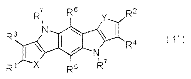 (式中、X、Y、R1~R7は前述と同じ。)
で表されるジカルコゲノベンゾジピロール化合物の製造方法。
<13> <1>~<7>のいずれかに記載のジカルコゲノベンゾジピロール化合物及び有機溶媒を含む組成物。
<14> <13>に記載の組成物を基板又は絶縁層上に塗布する工程と、基板又は絶縁層上に塗布された塗布膜を乾燥する工程とを含む薄膜の製造方法。
<1> 式(1)
で表されるジカルコゲノベンゾジピロール化合物。
<2> 前記式(1)において、X及びYが硫黄原子である<1>に記載のジカルコゲノベンゾジピロール化合物。
<3> 前記式(1)において、R3及びR4が、水素原子又はハロゲン原子であり、R7及びR8が、炭素数1~30のアルキル基、炭素数7~30のアリール基又は炭素数5~30のヘテロアリール基(該アリール基及び該ヘテロアリール基はフッ素原子で置換されていてもよいアルキル基又はフッ素原子で置換されていてもよいアルコキシ基を有する。)である<1>又は<2>に記載のジカルコゲノベンゾジピロール化合物。
<4> 前記式(1)において、R5及びR6が水素原子である<1>~<3>のいずれかに記載のジカルコゲノベンゾジピロール化合物。
<5> 前記式(1)において、R1~R4は、水素原子又はハロゲン原子である<1>~<4>のいずれかに記載のジカルコゲノベンゾジピロール化合物。
<6> 前記式(1)において、R7及びR8がフッ素原子で置換されていてもよいアルキル基を有する炭素数7~26のアリール基である<1>~<5>のいずれかに記載のジカルコゲノベンゾジピロール化合物。
<7> 前記式(1)において、R7及びR8がフッ素原子で置換されていてもよい炭素数1~20のアルキル基である<1>~<6>のいずれかに記載のジカルコゲノベンゾジピロール化合物。
<8> <1>~<7>のいずれかに記載のジカルコゲノベンゾジピロール化合物を含む薄膜。
<9> <1>~<7>のいずれかに記載のジカルコゲノベンゾジピロール化合物からなる薄膜。
<10> <8>又は<9>に記載の薄膜を含む有機トランジスタ。
<11> <8>又は<9>に記載の薄膜を含む有機半導体デバイス。
<12> 式(2)
と、式(3)
R7−NH2 (3)
(式中、R7は水素原子、ハロゲン原子、フッ素原子で置換されていてもよい炭素数1~30のアルキル基、フッ素原子で置換されていてもよい炭素数1~30のアルコキシ基、フッ素原子で置換されていてもよい炭素数2~30のアルケニル基、フッ素原子で置換されていてもよい炭素数2~30のアルキニル基、フッ素原子で置換されていてもよい炭素数1~30のアルキルチオ基、炭素数6~30のアリール基又は炭素数4~30のヘテロアリール基を表す。該アリール基及び該ヘテロアリール基は、フッ素原子、フッ素原子で置換されていてもよいアルキル基、フッ素原子で置換されていてもよいアルコキシ基、フッ素原子で置換されていてもよいアルケニル基、フッ素原子で置換されていてもよいアルキニル基及びフッ素原子で置換されていてもよいアルキルチオ基からなる群より選ばれる一以上を有していてもよい。)
で示されるアミン化合物とを反応させる工程を含む式(1’)
で表されるジカルコゲノベンゾジピロール化合物の製造方法。
<13> <1>~<7>のいずれかに記載のジカルコゲノベンゾジピロール化合物及び有機溶媒を含む組成物。
<14> <13>に記載の組成物を基板又は絶縁層上に塗布する工程と、基板又は絶縁層上に塗布された塗布膜を乾燥する工程とを含む薄膜の製造方法。
図1は、本発明における有機トランジスタの一つの態様を説明する断面図である。
図2は、本発明における有機トランジスタの一つの態様を説明する断面図である。
11は基板、12はゲート電極、13はゲート絶縁膜、14はソース電極、15はドレイン電極、16は有機半導体層を示す。21は基板、22はソース電極、23はドレイン電極、24はゲート絶縁膜、25はゲート電極、26は有機半導体層を示す。
図2は、本発明における有機トランジスタの一つの態様を説明する断面図である。
11は基板、12はゲート電極、13はゲート絶縁膜、14はソース電極、15はドレイン電極、16は有機半導体層を示す。21は基板、22はソース電極、23はドレイン電極、24はゲート絶縁膜、25はゲート電極、26は有機半導体層を示す。
本発明は、式(1)
 で表されるジカルコゲノベンゾジピロール化合物(「化合物(1)」)を提供する。
化合物(1)中、X及びYは、それぞれ独立して、硫黄原子、酸素原子、セレン原子、テルル原子又はSO2を表す。
化合物(1)のX及びYが同一であると、化合物(1)の合成が容易となるので、化合物(1)のX及びYが同一であることが好ましく、いずれも硫黄原子であることがより好ましい。
R1~R8は、それぞれ独立して、水素原子、ハロゲン原子、フッ素原子で置換されていてもよい炭素数1~30のアルキル基、フッ素原子で置換されていてもよい炭素数1~30のアルコキシ基、フッ素原子で置換されていてもよい炭素数2~30のアルケニル基、フッ素原子で置換されていてもよい炭素数2~30のアルキニル基、フッ素原子で置換されていてもよい炭素数1~30のアルキルチオ基、炭素数6~30のアリール基、炭素数4~30のヘテロアリール基を表す。該アリール基及び該ヘテロアリール基は、フッ素原子、フッ素原子で置換されていてもよいアルキル基、フッ素原子で置換されていてもよいアルコキシ基、フッ素原子で置換されていてもよいアルケニル基、フッ素原子で置換されていてもよいアルキニル基及びフッ素原子で置換されていてもよいアルキルチオ基からなる群より選ばれる一以上を有していてもよい。
R1~R4は、フッ素原子などのハロゲン原子又は水素原子であることが好ましい。
本発明における炭素数1~30のアルキル基は、直鎖、分枝鎖、及び環状のいずれでもよい。またR1~R8は、これらの水素原子の一部又は全てがフッ素原子で置換されたアルキル基であってもよい。
アルキル基としては、例えば、メチル基、エチル基、n−プロピル基、n−ブチル基、n−ペンチル基、n−ヘキシル基、n−ヘプチル基、n−オクチル基、n−ノニル基、n−デシル基、n−ウンデシル基、n−ドデシル基、n−トリデシル基、n−テトラデシル基、n−ペンタデシル基、n−ヘキサデシル基、n−ヘプタデシル基、n−オクタデシル基、n−ノナデシル基、n−イコシル基、n−ヘンイコシル基、n−ドコシル基、n−トリコシル基、n−テトラコシル基、n−ペンタコシル基、n−ヘキサコシル基、n−ヘプタコシル基、n−オクタコシル基、n−ノナコシル基、及びn−トリアコンチル基等の直鎖アルキル基;イソプロピル基、s−ブチル基、t−ブチル基、ネオペンチル基、2−エチルヘキシル基、2−ヘキシルデシル基等の分枝鎖アルキル基;シクロペンチル基、シクロヘキシル基、シクロオクチル基等の環状アルキル基を挙げることができる。
好ましくはメチル基、エチル基、n−プロピル基、イソプロピル基、n−ブチル基、s−ブチル基、t−ブチル基、n−ペンチル基、ネオペンチル基、n−ヘキシル基、2−エチルヘキシル基、シクロヘキシル基、n−ヘプチル基、n−オクチル基、シクロオクチル基、n−ノニル基、n−デシル基、2−ヘキシルデシル基、n−ウンデシル基、n−ドデシル基、n−トリデシル基、n−テトラデシル基、n−ペンタデシル基、n−ヘキサデシル基、n−ヘプタデシル基、n−オクタデシル基、n−ノナデシル基、n−イコシル基等の炭素数1~20のアルキル基であり、これらの水素原子の一部又は全てがフッ素原子で置換されたものも好ましい。より好ましくはエチル基、n−プロピル基、n−ブチル基、n−ペンチル基、n−ヘキシル基、2−エチルヘキシル基、シクロヘキシル基、n−ヘプチル基、n−オクチル基、n−ノニル基、n−デシル基、2−ヘキシルデシル基、n−ウンデシル基、n−ドデシル基、n−トリデシル基、2−ヘキシルオクチル基、n−テトラデシル基、n−ペンタデシル基、及びn−ヘキサデシル基等の炭素数2~16のアルキル基であり、これらの水素原子の一部又は全てがフッ素原子で置換されたものも好ましい。
本発明における炭素数1~30のアルコキシ基は、直鎖、分枝鎖及び環状のいずれでもよい。またR1~R8は、これらの水素原子の一部又は全てがフッ素原子で置換されたアルコキシ基であってもよい。
アルコキシ基としては、例えば、メトキシ基、エトキシ基、n−プロポキシ基、n−ブトキシ基、n−ペンチルオキシ基、n−ヘキシルオキシ基、n−ヘプチルオキシ基、n−オクチルオキシ基、n−デシルオキシ基、n−ウンデシルオキシ基、n−ドデシルオキシ基、n−トリデシルオキシ基、n−テトラデシルオキシ基、n−ペンタデシルオキシ基、n−ヘキサデシルオキシ基、n−ノニルオキシ基、n−ヘプタデシルオキシ基、n−オクタデシルオキシ基、n−ノナデシルオキシ基、n−イコシルオキシ基、n−ヘンイコシルオキシ基、n−ドコシルオキシ基、n−トリコシルオキシ基、n−テトラコシルオキシ基、n−ペンタコシルオキシ基、n−ヘキサコシルオキシ基、n−ヘプタコシルオキシ基、n−オクタコシルオキシ基、n−ノナコシルオキシ基、n−トリアコンチルオキシ基等の直鎖アルコキシ基;イソプロポキシ基、s−ブトキシ基、t−ブトキシ基、ネオペンチルオキシ基、2−エチルヘキシルオキシ基、2−ヘキシルデシルオキシ基、3,7−ジメチルオクチルオキシ基等の分枝鎖アルコキシ基;シクロヘキシルオキシ基、シクロオクチルオキシ基等の環状アルコキシ基等;メトキシメトキシ基、メトキシエトキシ基、メトキシメトキシメトキシ基、メトキシエトキシエトキシ基、ポリエチレングリコキシ基が挙げられる。
好ましくはメトキシ基、エトキシ基、n−プロポキシ基、イソプロポキシ基、n−ブトキシ基、s−ブトキシ基、t−ブトキシ基、n−ペンチルオキシ基、n−ヘキシルオキシ基、2−エチルヘキシルオキシ基、シクロヘキシルオキシ基、n−ヘプチルオキシ基、n−オクチルオキシ基、シクロオクチルオキシ基、n−ノニルオキシ基、n−デシルオキシ基、2−ヘキシルデシルオキシ基、3,7−ジメチルオクチルオキシ基、n−ウンデシルオキシ基、n−ドデシルオキシ基、n−トリデシルオキシ基、n−テトラデシルオキシ基、n−ペンタデシルオキシ基、n−ヘプタデシルオキシ基、n−オクタデシルオキシ基、n−ノナデシルオキシ基、n−イコシルオキシ基、メトキシメトキシ基、メトキシエトキシ基、メトキシメトキシメトキシ基、メトキシエトキシエトキシ基等の炭素数1~20のアルコキシ基であり、これらの水素原子の一部又は全てがフッ素原子で置換されたものも好ましい。より好ましくはエトキシ基、n−プロポキシ基、n−ブトキシ基、n−ペンチルオキシ基、n−ヘキシルオキシ基、2−エチルヘキシルオキシ基、シクロヘキシルオキシ基、n−ヘプチルオキシ基、n−オクチルオキシ基、n−ノニルオキシ基、n−デシルオキシ基、2−ヘキシルデシルオキシ基、n−ウンデシルオキシ基、n−ドデシルオキシ基、n−トリデシルオキシ基、n−テトラデシルオキシ基、n−ペンタデシルオキシ基、n−ヘキサデシルオキシ基、メトキシメトキシ基、メトキシエトキシ基、メトキシメトキシメトキシ基、メトキシエトキシエトキシ基の炭素数1~16のアルコキシ基が挙げられ、これらの水素原子の一部又は全てがフッ素原子で置換されたものも好ましい。
本発明におけるアルケニル基は炭素数2~30のアルケニル基であり、直鎖、分枝鎖及び環状のいずれでもよい。またR1~R8及びR13は、これらの水素原子の一部又は全てがフッ素原子で置換されたアルケニル基であってもよい。
アルケニル基としては、例えば、エテニル基、1−プロペニル基、1−ブテニル基、1−ペンテニル基、1−ヘキセニル基、1−ヘプテニル基、1−オクテニル基、1−ノネニル基、1−デセニル基、1−ウンデセニル基、1−ドデセニル基、1−トリデセニル基、1−テトラデセニル基、1−ペンタデセニル基、1−ヘキサデセニル基、1−ヘプタデセニル基、1−オクタデセニル基、1−ノナデセニル基、1−イコセニル基、1−ヘンイコセニル基、1−ドコセニル基、1−トリコセニル基、1−テトラコセニル基、1−ペンタコセニル基、1−ヘキサコセニル基、1−ヘプタコセニル基、1−オクタコセニル基、1−ノナコセニル基、1−トリアコンテニル基等の直鎖アルケニル基;1−メチル−1−プロペニル基等の分枝鎖アルケニル基;1−シクロヘキセニル基の環状アルケニル基が挙げられる。好ましくはエテニル基、1−プロペニル基、1−ブテニル基、1−ペンテニル基、1−ヘキセニル基、1−ヘプテニル基、1−オクテニル基、1−ノネニル基、1−デセニル基、1−ウンデセニル基、1−ドデセニル基、1−トリデセニル基、1−テトラデセニル基、1−ペンタデセニル基、1−ヘキサデセニル基、1−ヘプタデセニル基、1−オクタデセニル基、1−ノナデセニル基、及び1−イコセニル基等の炭素数2~20のアルケニル基であり、これらの水素原子の一部又は全てがフッ素原子で置換されたものも好ましい。より好ましくはエテニル基、1−プロペニル基、1−ブテニル基、1−ペンテニル基、1−ヘキセニル基、1−ヘプテニル基、1−オクテニル基、1−ノネニル基、1−デセニル基、1−ウンデセニル基、1−ドデセニル基、1−トリデセニル基、1−テトラデセニル基、1−ペンタデセニル基、1−ヘキサデセニル基等の炭素数2~16のアルケニル基であり、これらの水素原子の一部又は全てがフッ素原子で置換されたものも好ましい。
本発明における炭素数2~30のアルキニル基は、直鎖、分枝鎖及び環状のいずれでもよい。またR1~R8は、これらの水素原子の一部又は全てがフッ素原子で置換されたアルキニル基であってもよい。
アルキニル基としては、例えば、エチニル基、1−プロピニル基、1−ブチニル基、1−ペンチニル基、1−ヘキシニル基、1−ヘプチニル基、1−オクチニル基、1−ノニニル基、1−デシニル基、1−ウンデシル基、1−ドデシニル基、1−トリデシニル基、1−テトラデシニル基、1−ペンタデシニル基、1−ヘキサデシニル基、1−ヘプタデシニル基、1−オクタデシニル基、1−ノナデシニル基、1−イコシニル基、1−ヘンイコシニル基、1−ドコシニル基、1−トリコシニル基、1−テトラコシニル基、1−ペンタコシニル基、1−ヘキサコシニル基、1−ヘプタコシニル基、1−オクタコシニル基、1−ノナコシニル基、及び1−トリアコンチニル基が挙げられる。好ましくはエチニル基、1−プロピニル基、1−ブチニル基、1−ペンチニル基、1−ヘキシニル基、1−ヘプチニル基、1−オクチニル基、1−ノニニル基、1−デシニル基、1−ウンデシニル基、1−ドデシニル基、1−トリデシニル基、1−テトラデシニル基、1−ペンタデシニル基、1−ヘキサデシニル基、1−ヘプタデシニル基、1−オクタデシニル基、1−ノナデシニル基、及び1−イコシニル基等の炭素数2~20のアルキニル基であり、これらの水素原子の一部又は全てがフッ素原子で置換されたものも好ましい。より好ましくはエチニル基、1−プロピニル基、1−ブチニル基、1−ペンチニル基、1−ヘキシニル基、1−ヘプチニル基、1−オクチニル基、1−ノニニル基、1−デシニル基、1−ウンデシニル基、1−ドデシニル基、1−トリデシニル基、1−テトラデシニル基、1−ペンタデシニル基、及び1−ヘキサデシニル基等の炭素数2~16のアルキニル基であり、これらの水素原子の一部又は全てがフッ素原子で置換されたものも好ましい。
本発明における炭素数1~30のアルキルチオ基は、直鎖、分枝鎖及び環状のいずれでもよい。またR1~R8は、これらの水素原子の一部又は全てがフッ素原子で置換されたアルキルチオ基であってもよい。
アルキルチオ基としては、例えば、メチルチオ基、エチルチオ基、n−プロピルチオ基、イソプロピルチオ基、n−ブチルチオ基、n−ペンチルチオ基、n−ヘキシルチオ基、n−ヘプチルチオ基、n−オクチルチオ基、n−ノニルチオ基、n−デシルチオ基、n−ウンデシルチオ基、n−ドデシルチオ基、n−トリデシルチオ基、n−テトラデシルチオ基、n−ペンタデシルチオ基、n−ヘキサデシルチオ基、n−ヘプタデシルチオ基、n−オクタデシルチオ基、n−ノナデシルチオ基、n−イコシルチオ基、n−ヘンイコシルチオ基、n−ドコシルチオ基、n−トリコシルチオ基、n−テトラコシルチオ基、n−ペンタコシルチオ基、n−ヘキサコシルチオ基、n−ヘプタコシルチオ基、n−オクタコシルチオ基、n−ノナコシルチオ基、及びn−トリアコンチルチオ基等の直鎖アルキルチオ基;s−ブチルチオ基、t−ブチルチオ基、ネオペンチルチオ基、2−エチルヘキシルチオ基、2−ヘキシルデシルチオ基等の分枝鎖アルキルチオ基;シクロペンチルチオ基、シクロヘキシルチオ基、シクロオクチルチオ基等の環状アルキルチオ基が挙げられる。
好ましくはメチルチオ基、エチルチオ基、n−プロピルチオ基、イソプロピルチオ基、n−ブチルチオ基、s−ブチルチオ基、t−ブチルチオ基、n−ペンチルチオ基、ネオペンチルチオ基、n−ヘキシルチオ基、2−エチルヘキシルチオ基、シクロヘキシルチオ基、n−ヘプチルチオ基、n−オクチルチオ基、シクロオクチルチオ基、n−ノニルチオ基、n−デシルチオ基、2−ヘキシルデシルチオ基、n−ウンデシルチオ基、n−ドデシルチオ基、n−トリデシルチオ基、n−テトラデシルチオ基、n−ペンタデシルチオ基、n−ヘキサデシルチオ基、n−ヘプタデシルチオ基、n−オクタデシルチオ基、n−ノナデシルチオ基、n−イコシルチオ基等の炭素数1~20のアルキルチオ基であり、これらの水素原子の一部又は全てがフッ素原子で置換されたものも好ましい。より好ましくはメチルチオ基、エチルチオ基、n−プロピルチオ基、n−ブチルチオ基、n−ペンチルチオ基、n−ヘキシルチオ基、2−エチルヘキシルチオ基、シクロヘキシルチオ基、n−ヘプチルチオ基、n−オクチルチオ基、シクロオクチルチオ基、n−ノニルチオ基、n−デシルチオ基、2−ヘキシルデシルチオ基、n−ウンデシルチオ基、n−ドデシルチオ基、n−トリデシルチオ基、2−ヘキシルオクチルチオ基、n−テトラデシルチオ基、n−ペンタデシルチオ基、及びn−ヘキサデシルチオ基等の炭素数1~16のアルキルチオ基であり、これらの水素原子の一部又は全てがフッ素原子で置換されたものも好ましい。
本発明における炭素数6~30のアリール基としては、例えば、フェニル基、ナフチル基を挙げることができる。また、R1~R8は、水素原子の一部又は全てがフッ素原子で置換されたアリール基であってもよい。
さらに、R1~R8は、フッ素原子で置換されたアルキル基、フッ素原子で置換されたアルコキシ基、フッ素原子で置換されたアルケニル基、フッ素原子で置換されたアルキニル基及びフッ素原子で置換されたアルキルチオ基からなる群より選ばれる一以上を有するアリール基であってもよい。該アルキル基、該アルコキシ基、該アルケニル基、該アルキニル基及び該アルキルチオ基は上述の通りである。尚、置換基を有するアリール基の炭素数は、置換基を含めた全炭素数が7~30であることが好ましい。
R1~R8の好ましい例は、アルキル基又はアルコキシ基を有するアリール基である。好ましい具体例として、メチルフェニル基、エチルフェニル基、n−プロピルフェニル基、イソプロピルフェニル基、n−ブチルフェニル基、n−ペンチルフェニル基、n−ヘキシルフェニル基、n−ヘプチルフェニル基、n−オクチルフェニル基、n−ノニルフェニル基、n−デシルフェニル基、n−ウンデシルフェニル基、n−ドデシルフェニル基、n−トリデシルフェニル基及びn−テトラデシルフェニル基等の炭素数1~24の直鎖アルキル基を有するフェニル基;メトキシフェニル基、エトキシフェニル基、n−プロポキシフェニル基、n−ブトキシフェニル基、n−ペンチルオキシフェニル基、n−ヘキシルオキシフェニル基、n−ヘプチルオキシフェニル基、n−オクチルオキシフェニル基、n−デシルオキシフェニル基、n−ウンデシルオキシフェニル基、n−ドデシルオキシフェニル基、n−トリデシルオキシフェニル基、n−テトラデシルオキシフェニル基等の炭素数1~24の直鎖アルコキシ基を有するフェニル基が挙げられる。
本発明における炭素数4~30のヘテロアリール基は、例えば、チオフェニリル基、フラニル基、セレノフェニル基、ピローリル基、オキサゾーリル基、チアゾール基、ピリジニル基、ピラジニル基、ピリミジニル基、ピリダジニル基である。また、R1~R8は、水素原子の一部又は全てがフッ素原子で置換されたヘテロアリール基であってもよい。
さらに、R1~R8は、フッ素原子で置換されたアルキル基、フッ素原子で置換されたアルコキシ基、フッ素原子で置換されたアルケニル基、フッ素原子で置換されたアルキニル基及びフッ素原子で置換されたアルキルチオ基からなる群より選ばれる一以上を有するヘテロアリール基であってもよい。該アルキル基、該アルコキシ基、該アルケニル基、該アルキニル基及び該アルキルチオ基は上述の通りである。尚、置換基を有するヘテロアリール基の炭素数は、置換基を含めた全炭素数が7~16であることが好ましい。
本発明において、ハロゲン原子とは、フッ素原子、塩素原子、臭素原子及びヨウ素原子であり、R1~R8のハロゲン原子としてはフッ素原子が好ましい。
化合物(1)において、R1及びR2は、同一であることが好ましい。また、R1及びR2は、水素原子又はフッ素原子などのハロゲン原子であることが好ましい。R3及びR4は、同一であることが好ましい。また、R1及びR2は、水素原子又はフッ素原子などのハロゲン原子であることが好ましい。
化合物(1)において、R1~R4の全てが水素原子であるものが好ましい。
また、化合物(1)において、R5及びR6が共に水素原子であるものが好ましい。
化合物(1)において、R7及びR8が同一であり、R7及びR8が、フッ素原子で置換されたアルキル基を有していてもよい全炭素数7~26のアリール基であることが好ましい。
好ましいR7及びR8の具体例は、メチルフェニル基、エチルフェニル基、n−プロピルフェニル基、イソプロピルフェニル基、n−ブチルフェニル基、n−ペンチルフェニル基、n−ヘキシルフェニル基、n−ヘプチルフェニル基、n−オクチルフェニル基、n−ノニルフェニル基、n−デシルフェニル基、n−ウンデシルフェニル基、n−ドデシルフェニル基、n−トリデシルフェニル基及びn−テトラデシルフェニル基等の炭素数1~14の直鎖アルキル基を有するフェニル基;例えば、メトキシフェニル基、エトキシフェニル基、n−プロポキシフェニル基、n−ブトキシフェニル基、n−ペンチルオキシフェニル基、n−ヘキシルオキシフェニル基、n−ヘプチルオキシフェニル基、n−オクチルオキシフェニル基、n−デシルオキシフェニル基、n−ウンデシルオキシフェニル基、n−ドデシルオキシフェニル基、n−トリデシルオキシフェニル基、n−テトラデシルオキシフェニル基である。
化合物(1)において、R7及びR8は、同一であり、R7及びR8が、フッ素原子で置換されていてもよい炭素数1~20のアルキル基であることも好ましい。
好ましいR7及びR8の具体例は、メチル基、エチル基、n−プロピル基、イソプロピル基、n−ブチル基、s−ブチル基、t−ブチル基、n−ペンチル基、ネオペンチル基、n−ヘキシル基、2−エチルヘキシル基、シクロヘキシル基、n−ヘプチル基、n−オクチル基、シクロオクチル基、n−ノニル基、n−デシル基、2−ヘキシルデシル基、n−ウンデシル基、n−ドデシル基、n−トリデシル基、n−テトラデシル基、n−ペンタデシル基、n−ヘキサデシル基、n−ヘプタデシル基、n−オクタデシル基、n−ノナデシル基、n−イコシル基等の炭素数1~20のアルキル基等及びこれらの基の水素原子の一部又は全てがフッ素原子で置換された基である。
化合物(1)の例を、表1~8に記載する。
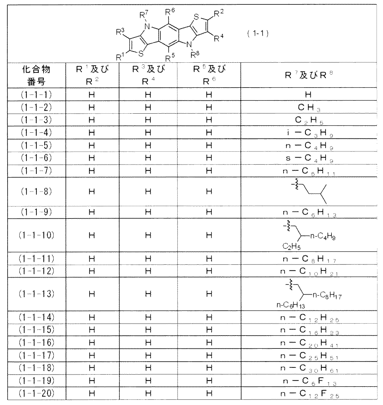
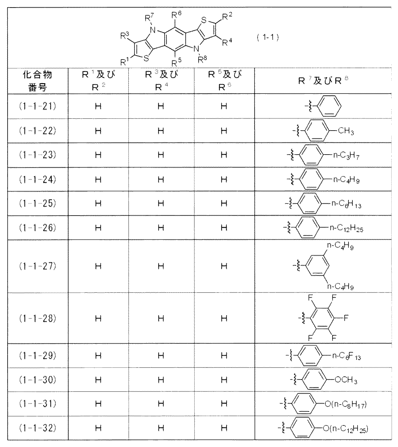
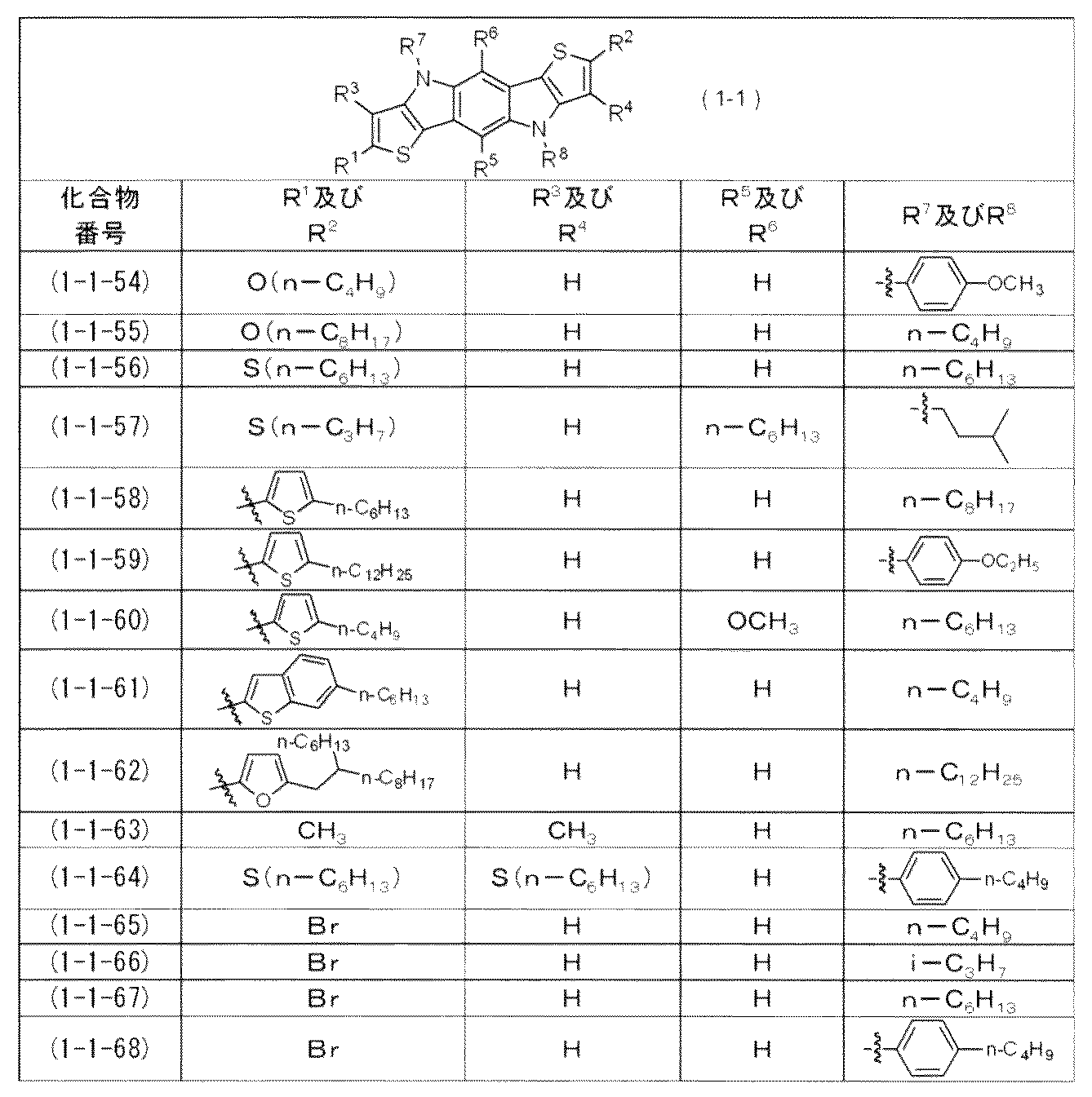
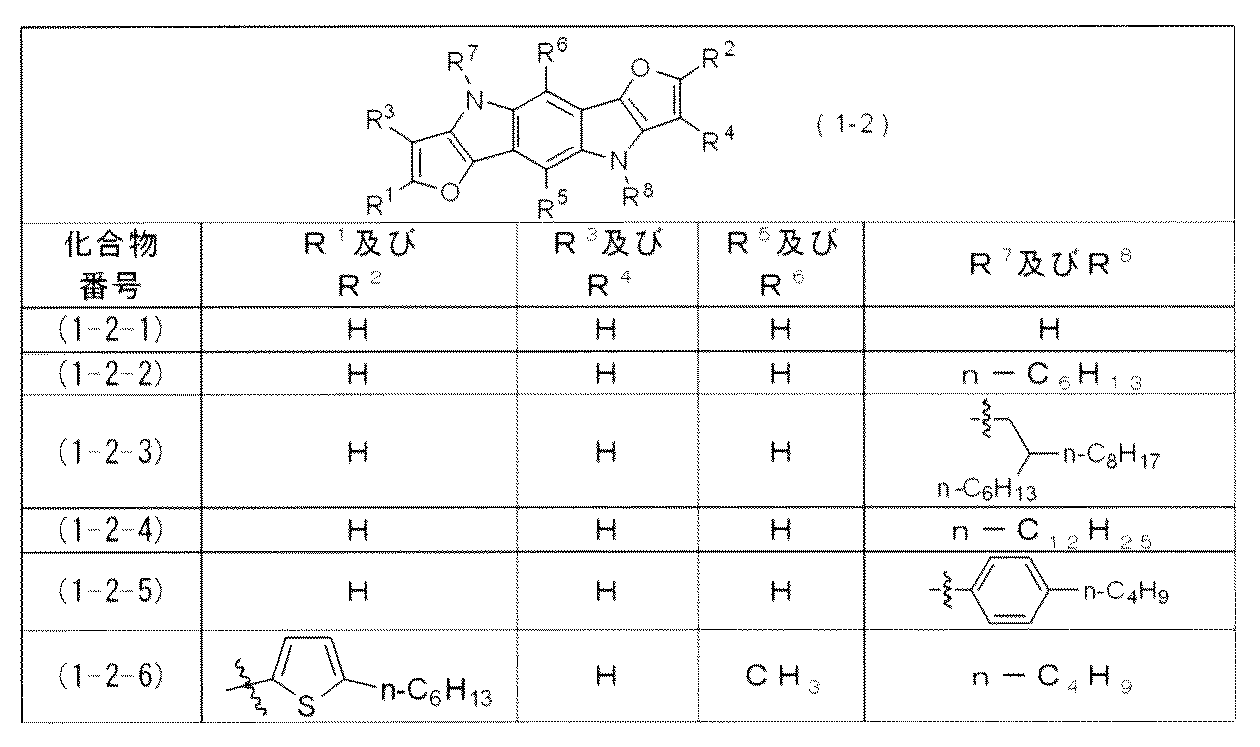
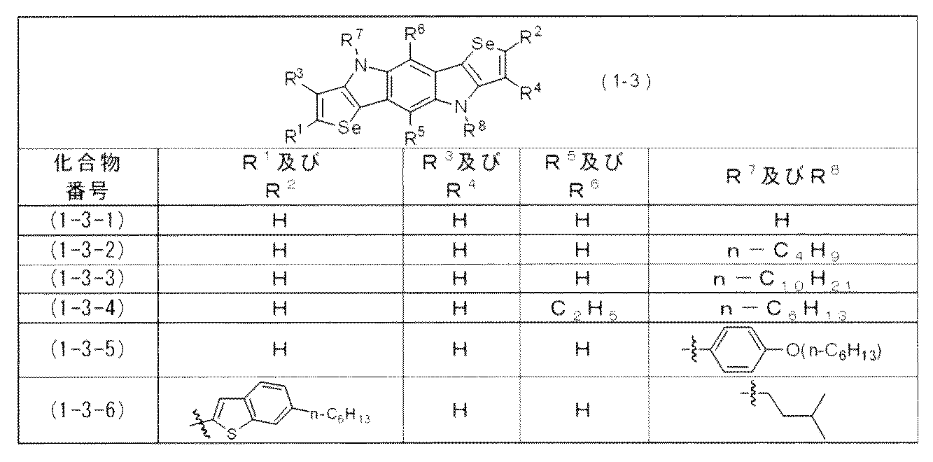

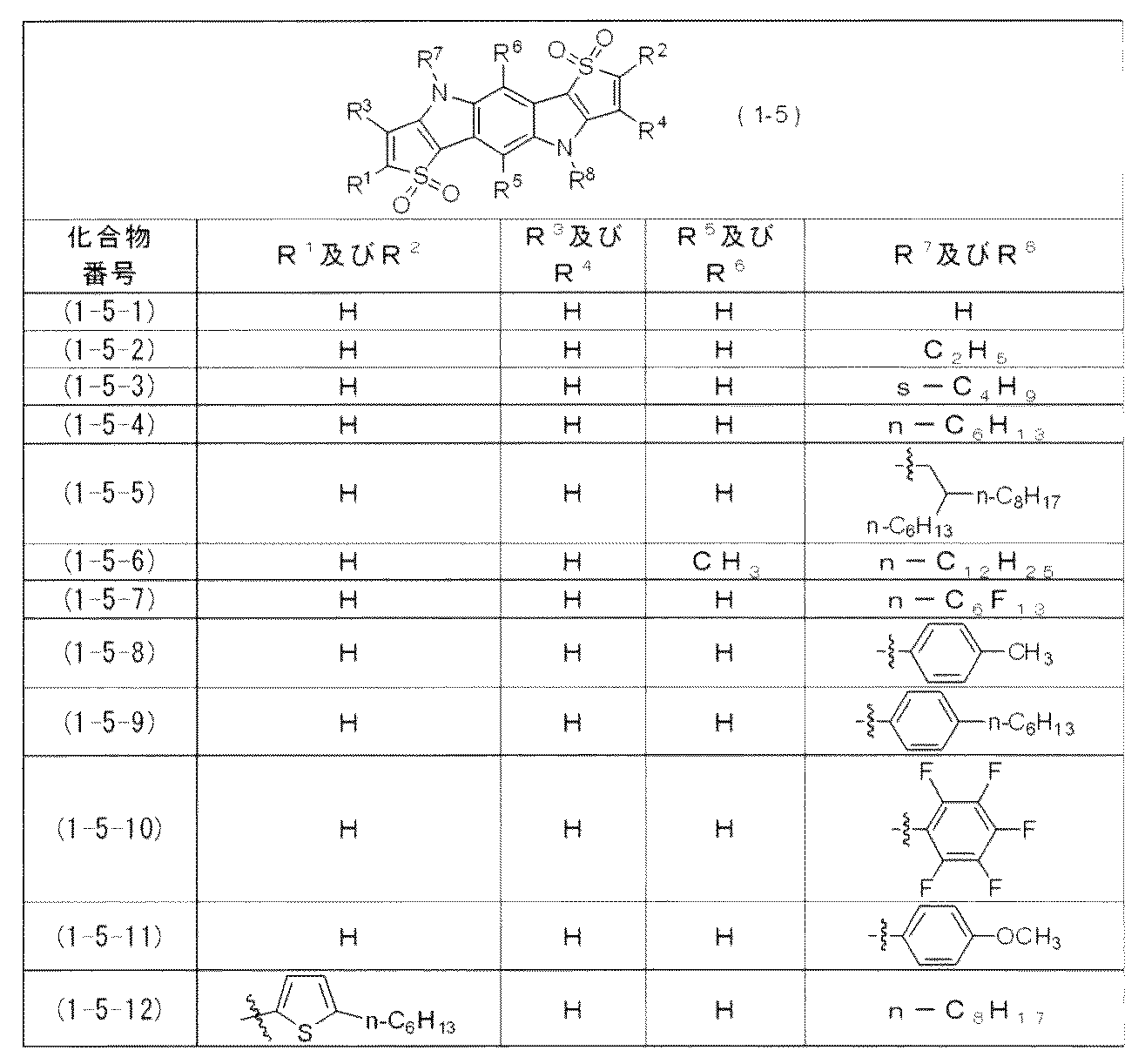
表1~8において、波線は結合手を表す。
好ましい化合物(1)は、表中に示された化合物番号で表すと、例えば、(1−1−1)、(1−1−2)、(1−1−3)、(1−1−4)、(1−1−5)、(1−1−6)、(1−1−8)、(1−1−9)、(1−1−11)、(1−1−12)、(1−1−13)、(1−1−14)、(1−1−15)、(1−1−19)、(1−1−21)、(1−1−22)、(1−1−24)、(1−1−25)、(1−1−26)、(1−1−28)、(1−1−29)、(1−1−30)、(1−1−31)、(1−1−33)、(1−1−35)、(1−1−42)、(1−1−45)、(1−1−51)、(1−1−52)、(1−1−56)、(1−1−58)、(1−1−59)、(1−1−61)、(1−1−64)、(1−1−65)、(1−1−67)、(1−1−68)、(1−2−2)、(1−2−7)、(1−3−3)、(1−3−6)、(1−4−2)、(1−5−4)、(1−5−5)、(1−5−7)、(1−5−9)、(1−5−11)、(1−5−12)であり、さらに好ましいものは、(1−1−1)、(1−1−2)、(1−1−3)、(1−1−5)、(1−1−6)、(1−1−9)、(1−1−11)、(1−1−12)、(1−1−13)、(1−1−14)、(1−1−21)、(1−1−22)、(1−1−24)、(1−1−25)、(1−1−26)、(1−1−30)、(1−1−31)、(1−1−33)、(1−1−45)、(1−1−58)、(1−1−61)である。
本発明の化合物(1)は、後述するように、真空プロセスで薄膜を形成することができる。また、化合物(1)は有機溶媒への溶解性に優れることから、溶液プロセスによって薄膜を形成することができる。ここで、溶解可能な有機溶媒としては、例えば、水、メタノール、エタノール、イソプロピルアルコール、ブタノール等のアルコール溶媒、ベンゼン、トルエン、キシレン、クロロベンゼン、o−ジクロロベンゼン、トリクロロベンゼン、フルオロベンゼン等の芳香族炭化水素溶媒、例えばジクロロメタン、クロロホルム、1,2−ジクロロエタン、1,1’,2,2’−テトラクロロエタン、テトラクロロエチレン、四塩化炭素等のハロゲン化脂肪族炭化水素溶媒、例えばジエチルエーテル、ジオキサン、テトラヒドロフラン、アニソール等のエーテル溶媒、例えばペンタン、ヘキサン、ペンタン、オクタン、シクロヘキサン等の脂肪族炭化水素溶媒、アセトン、メチルエチルケトン、メチルイソブチルケトン、シクロヘキサノン等のケトン溶媒、酢酸エチル、酢酸ブチル等のエステル溶媒、アセトニトリル、プロピオニトリル、メトキシアセトニトリル、グルタロジニトリル、ベンゾニトリルなどのニトリル溶媒、ジメチルスルホキシド、スルホラン、N,N−ジメチルホルムアミド、N,N−ジメチルアセトアミド、N−メチル−2−ピロリドンなどの非プロトン性極性溶媒が挙げられ、中でも、トルエン、キシレン、o−ジクロロベンゼン、ジクロロメタン、クロロホルム、テトラヒドロフランが好ましい。溶媒は、2種以上を混合して用いることもできる。
化合物(1)を含む有機溶液における化合物(1)の濃度は、通常、0.001~50重量%の範囲内であり、好ましくは0.01~10重量%、より好ましくは0.1~5重量%の範囲内である。
該有機溶液には、化合物(1)のみならず、酸化防止剤、安定剤、有機半導体材料、有機絶縁性材料などを、後述する有機半導体層である薄膜のキャリア移動度を著しく損なわない量で含有されていてもよい。
該有機半導体材料としては、低分子材料でもよく、高分子材料でもよく、架橋反応が可能な場合は架橋していてもよく架橋していなくてもよい。好ましくは、高分子材料が挙げられる。具体例としては、ポリアセチレン誘導体、ポリチオフェン誘導体、ポリチエニレンビニレン誘導体、ポリフェニレン誘導体、ポリフェニレンビニレン誘導体、ポリピロール誘導体、ポリアニリン誘導体、ポリトリアリールアミン誘導体、ポリキノリン誘導体、ペリレン誘導体、テトラセン誘導体、ペンタセン誘導体、フタロシアニン誘導体などが挙げられ、この場合、化合物(1)の含有量は、10重量%以上が好ましく、20重量%以上になるように調整することがより好ましい。
該有機絶縁性材料としては、低分子材料でもよく、高分子材料でもよく、架橋反応が可能な場合は架橋していてもよく架橋していなくてもよい。好ましくは、高分子材料が挙げられる。具体例としては、ポリスチレン、ポリカーボネート、ポリジメチルシロキサン、ナイロン、ポリイミド、環状オレフィンコポリマー、エポキシポリマー、セルロース、ポリオキシメチレン、ポリオレフィン系ポリマー、ポリビニル系ポリマー、ポリエステル系ポリマー、ポリエーテル系ポリマー、ポリアミド系ポリマー、フッ素系ポリマー、生分解性プラスチック、フェノール系樹脂、アミノ樹脂、不飽和ポリエステル樹脂、ジアリルフタレート樹脂、エポキシ樹脂、ポリイミド樹脂、ポリウレタン樹脂、シリコーン樹脂、及び各種ポリマーユニットを組み合わせたコポリマーなどが挙げられ、この場合、化合物(1)の含有量は、10重量%以上が好ましく、20重量%以上になるように調整することがより好ましい。
有機溶液の調製方法としては、有機溶媒に化合物(1)を、例えば、10~200℃の範囲等、好ましくは20~150℃の範囲等で溶解することによって得ることができる。
本発明の化合物(1)は、例えば、式(2)
 (式中、R1~R6、X及びYは前記と同じ定義であり、R9~R12は、それぞれ独立して、ハロゲン原子、好ましくは、臭素又はヨウ素を表す。)
で表される化合物(化合物(2))と、式
R7−NH2 及び R8−NH2
(式中、R7及びR8は、水素原子、ハロゲン原子、フッ素原子で置換されていてもよい炭素数1~30のアルキル基、フッ素原子で置換されていてもよい炭素数1~30のアルコキシ基、フッ素原子で置換されていてもよい炭素数2~30のアルケニル基、フッ素原子で置換されていてもよい炭素数2~30のアルキニル基、フッ素原子で置換されていてもよい炭素数1~30のアルキルチオ基、炭素数6~30のアリール基又は炭素数4~30のヘテロアリール基を表す。該アリール基及び該ヘテロアリール基は、フッ素原子、フッ素原子で置換されていてもよいアルキル基、フッ素原子で置換されていてもよいアルコキシ基、フッ素原子で置換されていてもよいアルケニル基、フッ素原子で置換されていてもよいアルキニル基又はフッ素原子で置換されていてもよいアルキルチオ基を有していてもよい。)
で示されるアミン化合物とを反応させることにより製造することができる。
アミン化合物として式(3)
R7−NH2 (3)
(式中、R7は水素原子、ハロゲン原子、フッ素原子で置換されていてもよい炭素数1~30のアルキル基、フッ素原子で置換されていてもよい炭素数1~30のアルコキシ基、フッ素原子で置換されていてもよい炭素数2~30のアルケニル基、フッ素原子で置換されていてもよい炭素数2~30のアルキニル基、フッ素原子で置換されていてもよい炭素数1~30のアルキルチオ基、炭素数6~30のアリール基又は炭素数4~30のヘテロアリール基を表す。該アリール基及び該ヘテロアリール基は、フッ素原子、フッ素原子で置換されていてもよいアルキル基、フッ素原子で置換されていてもよいアルコキシ基、フッ素原子で置換されていてもよいアルケニル基、フッ素原子で置換されていてもよいアルキニル基又はフッ素原子で置換されていてもよいアルキルチオ基を有していてもよい。)
で示されるアミン化合物のみを用いると、前述の式(1’)で表されるジカルコゲノベンゾジピロール化合物が製造される。
化合物(1)の製造に用いられる化合物(2)としては、例えば下表の化合物が挙げられる。
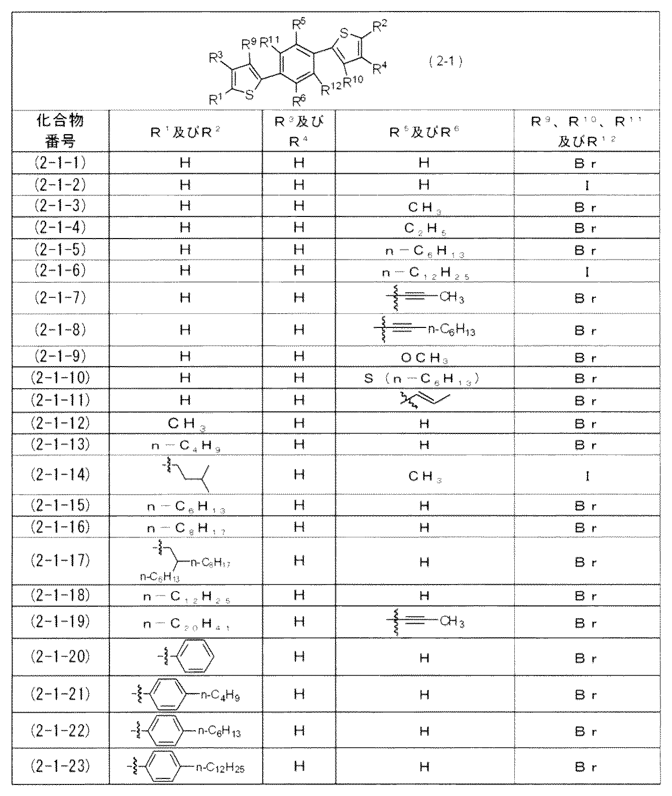
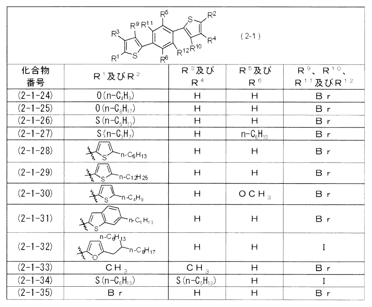


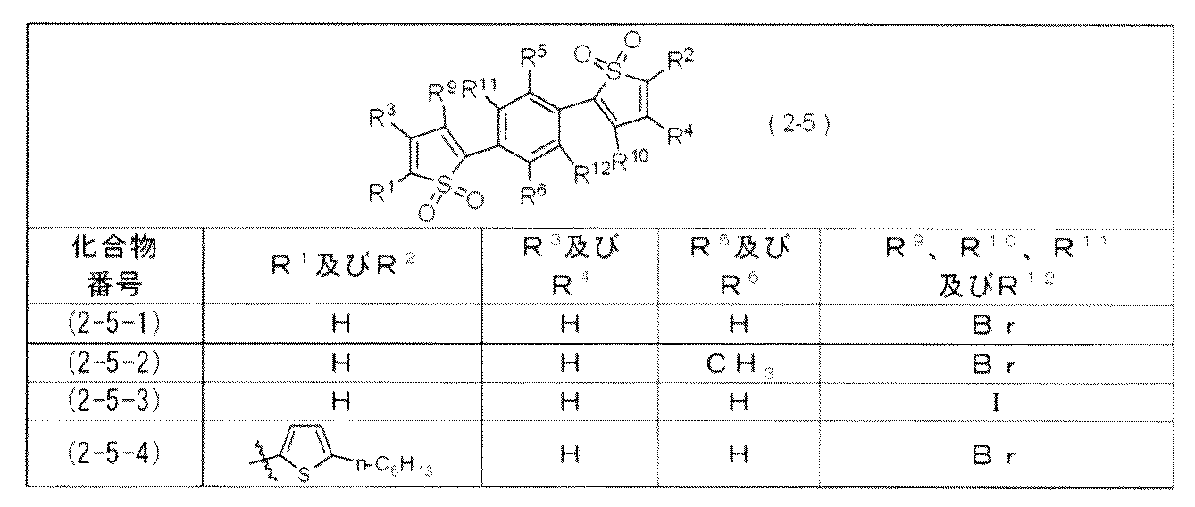
表9~14において、波線は結合手を表す。
反応に用いられるアミン化合物としては、例えば、メチルアミン、エチルアミン、n−プロピルアミン、イソプロピルアミン、n−ブチルアミン、n−ペンチルアミン、n−ヘキシルアミン、n−ヘプチルアミン、n−オクチルアミン、n−ノニルアミン、n−デシルアミン、n−ウンデシルアミン、n−ドデシルアミン、n−トリデシルアミン、n−テトラデシルアミン、n−ペンタデシルアミン、n−ヘキサデシルアミン、n−ヘプタデシルアミン、n−オクタデシルアミン、n−ノナデシルアミン、n−イコシルアミン、n−ヘンイコシルアミン、n−ドコシルアミン、n−トリコシルアミン、n−テトラコシルアミン、n−ペンタコシルアミン、n−ヘキサコシルアミン、n−ヘプタコシルアミン、n−オクタコシルアミン、n−ノナコシルアミン、及びn−トリアコンチルアミン等の直鎖アルキルアミン;アニリン、4−メチルアニリン、4−エチルアニリン、4−n−プロピルアニリン、4−イソプロピルアニリン、4−n−ブチルアニリン、4−n−ペンチルアニリン、4−n−ヘキシルアニリン、4−n−ヘプチルアニリン、4−n−オクチルアニリン、4−n−ノニルアニリン、4−n−デシルアニリン、4−n−ウンデシルアニリン、4−n−ドデシルアニリン、4−n−トリデシルアニリン、4−n−テトラデシルアニリン等のアルキル基を有するアニリンを挙げることができる。
反応に用いられるアミン化合物の使用量は、化合物(2)1モルに対して、通常、1~50モル、好ましくは2~20モル、より好ましくは2~15モルの割合である。
反応は、有機溶媒中で行うことが好ましい。
上記有機溶媒としては、上記の反応に不活性な有機溶媒であればよく、例えば、トルエン、キシレン、等の芳香族炭化水素溶媒;クロロベンゼン、o−ジクロロベンゼン等のハロゲン原子化芳香族炭化水素溶媒;ヘキサン、ヘプタン、ジメトキシエタン等の脂肪族炭化水素溶媒;クロロホルム、1,2−ジクロロエタン等のハロゲン原子化脂肪族炭化水素溶媒;メタノール、イソプロピルアルコール、t−ブチルアルコール等の炭素数1~4のアルコール;テトラヒドロフラン、ジオキサン等のエーテル溶媒;それらの混合溶媒が挙げられ、好ましくは芳香族炭化水素溶媒及び脂肪族炭化水素溶媒が挙げられ、より好ましくはトルエンやキシレンが挙げられる。
反応液における化合物(2)の濃度は、有機溶媒1リットル当たり、例えば、0.0001~20モル、好ましくは、0.001~10モル、より好ましくは、0.01~5モルである。
反応は、パラジウム触媒及び塩基の存在下で行われることが好ましい。
パラジウム触媒の使用量は、化合物(2)100モルに対して、パラジウム原子換算で、通常、0.01~50モル、好ましくは0.01~30モルの割合である。
パラジウム触媒は、配位子になる化合物とパラジウム化合物とを予め有機溶媒中で接触させることにより調製したものを用いてもよいし、配位子になる化合物とパラジウム化合物とを反応系内で接触させて調製したものを用いてもよい。
上記の配位子になる化合物としては、パラジウムに配位可能であって有機溶媒に可溶であればよく、例えば単座ホスフィン系配位子、多座配位子、カルベン系配位子等が挙げられ、単座配位子が好ましく、単座ホスフィン系配位子がより好ましい。
単座ホスフィン系配位子としては、例えば、トリ(n−ブチル)ホスフィン、トリ(t−ブチル)ホスフィン、トリシクロヘキシルホスフィン、トリフェニルホスフィン、トリ(o−トリル)ホスフィン、トリナフチルホスフィン、ジフェニルナフチルホスフィン及びジシクロヘキシルナフチルホスフィンが挙げられ、トリ(t−ブチル)ホスフィンが好ましい。
二座配位子としては、例えば、2,2’−ビス(ジフェニルホスフィノ)−1,1’−ビナフチル、1,2−ビス(ジフェニルホスフィノ)エタン、1,3−ビス(ジフェニルホスフィノ)プロパン、1,4−ビス(ジフェニルホスフィノ)ブタン、1,1’−(ジフェニルホスフィノ)フェロセン、4,5−ビス(ジフェニルホスフィノ)−9,9−ジメチルキサンテン、2,2’−ビス(ジフェニルホスフィノ)ジフェニルエーテル、5,5’−ビス(ジフェニルホスフィノ)−4,4’−ビ(1,3−ベンゾジオキソール)等のリン原子を2つ有する二座ホスフィン系配位子;2−(N,N−ジメチルアミノ)−2’−(ジシクロヘキシルアミノ)ビフェニル等の窒素原子及びリン原子をそれぞれ1つずつ有する二座アミノホスフィン系配位子が挙げられる。
かかる配位子は、市販品をそのまま用いてもよいし、公知の方法により製造したものを用いてもよい。
かかる配位子の使用量は、パラジウム化合物のパラジウム原子1モルに対して、0.5~20モルの割合がよい。
上記パラジウム化合物としては、酢酸パラジウム、塩化パラジウム、ジクロロビス(アセトニトリル)パラジウム、パラジウムアセチルアセトナート、ジクロロ(シクロオクタ−1,5−ジエン)パラジウム、ジブロモビス(ベンゾニトリル)パラジウム、ジ−μ−クロロビス(π−アリル)ジパラジウム、ジクロロビス(ピリジン)パラジウム、ジクロロビス(トリフェニルホスフィン)パラジウム、ジクロロ−[1,1’−ビス(ジフェニルホスフィノ)フェロセン]パラジウム・ジクロロメタン錯体等の2価のパラジウム化合物;トリス(ジベンジリデンアセトン)ジパラジウム、トリス(ジベンジリデンアセトン)ジパラジウム・クロロホルム錯体、テトラキス(トリフェニルホスフィン)パラジウム等の0価のパラジウム化合物;等が挙げられ、中でもトリス(ジベンジリデンアセトン)ジパラジウム、トリス(ジベンジリデンアセトン)ジパラジウム・クロロホルム錯体が好ましい。かかるパラジウム化合物は、市販品をそのまま用いてもよいし、公知の方法により製造したものを用いてもよい。
塩基としては、例えば、水酸化カルシウム等のアルカリ土類金属水酸化物;炭酸カリウム、炭酸ナトリウム、炭酸セシウム等のアルカリ金属炭酸塩;炭酸マグネシウム、炭酸カルシウム、炭酸バリウム等のアルカリ土類金属炭酸塩;リン酸リチウム、リン酸カリウム、リン酸ナトリウム等のアルカリ金属リン酸塩;ナトリウムメトキシド、ナトリウムエトキシド、ナトリウムt−ブトキシド、カリウムメトキシド、カリウムエトキシド、カリウムt−ブトキシド、リチウムt−ブトキシド等のアルカリ金属アルコキシドが挙げられ、好ましくは、アルカリ金属炭酸塩、アルカリ金属アルコキシドが挙げられ、より好ましくはアルカリ金属アルコキシド、更に好ましくは炭素数1~6のアルカリ金属アルコキシドが挙げられる。塩基は単独で用いてもよいし、2種類以上を混合して用いてもよい。
塩基の使用量は、化合物(2)1モルに対して、例えば、0.1~25モル、好ましくは1~20モル、更に好ましくは2~10モルの割合である。塩基の使用量が25モル以下であると、未反応のアミン化合物(3)の割合が低減される傾向があることから好ましい。
反応温度は、0℃から反応液の還流温度の範囲内から選ばれるが、好ましくは40~200℃の範囲内である。反応時間は、通常、1分から120時間の範囲内である。
反応を停止させるに際し、例えば、反応液に水、希塩酸などを添加する。反応停止後、例えば抽出、洗浄等の後処理操作を行うことで、化合物(1)の粗生成物を得ることができる。粗生成物は、晶析、昇華、又は各種クロマトグラフィーなどの精製操作、若しくはこれらを組み合わせた精製操作を行うことにより精製を行うことができる。
化合物(2)の製造方法としては、例えば、US2011/168953記載の方法に準拠して、一般式(4)
 (式中、R5及びR6は上記と同じ定義である。R14~R17は、それぞれハロゲン原子を表す。)
で表される化合物(化合物(4))と
一般式(5)
 (式中、Xは上記と同じ定義である。R18及びR19は、それぞれハロゲン原子を表す。)
で表される化合物(化合物(5))とを、遷移金属触媒存在下、根岸カップリング反応に供することで製造することができる。
本発明の薄膜は、化合物(1)を含む薄膜であり、例えば、厚み1nm~10μm、好ましくは厚み5nm~1μmの薄膜である。
本発明の薄膜は発光性、半導体と同様の導電性を示す場合があり、それぞれ、発光性薄膜、導電性薄膜としても優れている。
本発明において発光性薄膜とは、化合物(1)を含む薄膜であって、光や電気的刺激の条件下で発光する薄膜を意味する。発光性薄膜は、発光素子の材料として有用である。発光性薄膜を有する発光素子もまた、本発明の一つである。本発明の発光素子は、例えば有機発光ダイオード等の材料として有用である。
本発明において、発光素子とは該発光性薄膜を用いたデバイスのことを意味する。
本発明において、導電性薄膜とは、光や電気的刺激の条件下で導電性を示す薄膜を意味する。半導体と同様の導電性を示す導電性薄膜を特に有機半導体薄膜と称することがある。導電性薄膜は、後述の有機半導体デバイス等の材料として有用である。
本発明の導電性薄膜及び発光性薄膜は、それぞれ、本発明の化合物(1)を材料として用いる以外は、従来公知の方法と同様に製造することができる。
次に、有機トランジスタについて説明する。
本発明の有機トランジスタは、本発明の薄膜を含むものである。
上記該有機トランジスタは、本発明の化合物(1)を含んでいるので、キャリア移動度が高い。上記該有機トランジスは、キャリア移動度を10−6cm2/Vs以上とすることができる。ここでキャリア移動度は、パラメータアナライザー等を用いて測定したドレイン電流及びゲート電圧について、下記式(a)を適用することにより測定することができる。
Id=(W/2L)μCi(Vg−Vt)2 ・・・(a)
(式中、Id=電気的特性の飽和領域におけるドレイン電流、L=有機トランジスタのチャネル長、W=有機トランジスタのチャネル幅、Ci=ゲート絶縁膜の単位面積当たりの容量、Vg=ゲート電圧、Vt=ゲート電圧のしきい値電圧)
本発明の有機トランジスタとしては、有機電界効果トランジスタが挙げられる。
該有機電界効果トランジスタは、通常、ソース電極及びドレイン電極が半導体層に接しており、さらに活性層に接した絶縁層(誘電体層)を挟んでゲート電極が設けられていればよい。
上記有機トランジスタの素子構造としては、例えば、
(1)基板/ゲート電極/絶縁体層/ソース電極・ドレイン電極/半導体層からなる構造;
(2)基板/ゲート電極/絶縁体層/半導体層/ソース電極・ドレイン電極からなる構造(図1参照);
(3)基板/半導体層+ソース電極・ドレイン電極/絶縁体層/ゲート電極からなる構造(図2参照);
(4)基板/ソース電極(又はドレイン電極)/半導体層+絶縁体層+ゲート電極/ドレイン電極(又はソース電極)からなる構造、
が挙げられる。
上記各構造において、半導体層は、本発明の有機半導体薄膜を有する。各構造において該半導体層が複数である場合、同一平面内に設けてもよいし、積層して設けてもよい。上記各構造において、ソース電極、ドレイン電極、及びゲート電極は、それぞれ複数設けてもよい。
有機トランジスタにおける薄膜として、化合物(1)が含まれる有機半導体層を形成する方法は、例えば、真空蒸着法、スパッタリング法、CVD法、分子線エピタキシャル成長法などの真空プロセスでの形成法が挙げられ、好ましくは真空蒸着法が挙げられる。
真空蒸着法とは、化合物(1)などの有機半導体材料をルツボや金属ボート中で真空下、加熱し、蒸発した有機半導体材料を基板もしくは絶縁体材料に蒸着させる方法である。
蒸着時の真空度は、1×10⁻¹Pa以下、好ましくは1×10⁻³Pa以下である。
蒸着時の基板温度は0℃~300℃、好ましくは20℃~200℃である。
蒸着速度は、0.001nm/sec~10nm/secであり、好ましくは0.01nm/sec~1nm/secである。上記有機半導体薄膜の膜厚は、1nm~10μmであり、好ましくは5nm~1μmである。
有機トランジスタにおける薄膜として、化合物(1)が含まれる有機半導体層を形成する方法の異なる実施態様は、化合物(1)が有機溶媒に対する溶解性に優れていることから、塗布成膜加工を例示することができる。塗布成膜加工は、通常、化合物(1)を有機溶媒に溶解して得られる溶液状の組成物を調製し、該組成物を基板もしくは絶縁体層に塗布する工程と、該基板上に塗布された塗布膜を乾燥する工程を有する。塗布する工程としては、例えば、キャスティング法、ディップコート法、ダイコーター法、ロールコーター法、バーコーター法、スピンコート法などの塗布法、インクジェット法、スクリーン印刷法、オフセット印刷法、マイクロコンタクト印刷法などが挙げられる。これらの工程は、単独で用いてもよいし、2種以上を組み合わせてもよい。
塗布する工程によって得られた塗布膜は、乾燥、すなわち、組成物に含まれる有機溶媒を除去することで、本発明の薄膜を得ることができる。乾燥方法としては、例えば、自然乾燥処理、加熱処理、減圧処理、通風処理又はこれらを組み合わせた処理等を挙げることができ、操作が簡便である点で自然乾燥処理もしくは加熱処理が好ましい。具体的には、大気下で放置もしくはホットプレートで基板加熱(例えば、40~250℃、好ましくは、50~200℃)する処理等が挙げられる。
組成物としては、化合物(1)は有機溶媒に溶解していなくとも、化合物(1)を溶媒に分散させていてもよい。この場合の具体的な実施態様は、前述の組成物が、化合物(1)を溶媒に分散させた分散液であることを意味する。
有機トランジスタにおける薄膜を有機半導体層として形成する方法としては、化合物(1)を有機溶媒で溶解させて得られる組成物を用いた塗布成膜加工が好ましい。かかる薄膜から得られる有機トランジスタは優れたキャリア移動度を示す。
本発明の有機トランジスタにおいて、ソース電極、ドレイン電極及びゲート電極を構成する材料は、一般的な導電性材料であれば特に限定されず、白金、金、銀、ニッケル、クロム、銅、鉄、錫、アンチモン鉛、タンタル、インジウム、パラジウム、テルル、レニウム、イリジウム、アルミニウム、ルテニウム、ゲルマニウム、モリブデン、タングステン、酸化スズ・アンチモン、酸化インジウム・スズ(ITO)、フッ素ドープ酸化亜鉛、亜鉛、炭素、グラファイト、グラッシーカーボン、銀ペースト及びカーボンペースト、リチウム、ベリリウム、ナトリウム、マグネシウム、カリウム、カルシウム、スカンジウム、チタン、マンガン、ジルコニウム、ガリウム、ニオブ、ナトリウム、ナトリウム−カリウム合金、マグネシウム、リチウム、アルミニウム、マグネシウム/銅混合物、マグネシウム/銀混合物、マグネシウム/アルミニウム混合物、マグネシウム/インジウム混合物、アルミニウム/酸化アルミニウム混合物、及びリチウム/アルミニウム混合物、酸化モリブデン等が用いられるが、
特に、白金、金、銀、銅、アルミニウム、ニッケル、インジウム、ITO、炭素、及び酸化モリブデンが好ましい。あるいはドーピング等で導電率を向上させた公知の導電性ポリマー、例えば、導電性ポリアニリン、導電性ポリピロール、導電性ポリチオフェン、ポリエチレンジオキシチオフェンとポリスチレンスルホン酸の錯体等も好適に用いられる。中でも半導体層との接触面において電気抵抗が少ないものが好ましい。これらの電極材料は単独で使用してもよいし、2種類以上を混合して使用してもよい。
電極の膜厚は、材料によっても異なるが、0.1nm~10μmであればよく、好ましくは0.5nm~5μmであり、より好ましくは1nm~3μmである。また、ゲート電極と基板を兼ねる場合は上記の膜厚より大きくてもよい。
電極膜の形成方法としては、公知の種々の方法が挙げられる。具体的には、真空蒸着法、スパッタ法、塗布法、熱転写法、印刷法、ゾルゲル法などが挙げられる。成膜時又は成膜後に、パターニングを必要に応じて行うことが好ましい。パターニングの方法としても、種々の方法を用いることができる。具体的には、フォトレジストのパターニングとエッチングを組み合わせたフォトリソグラフィー法などが挙げられる。また、インクジェット印刷、スクリーン印刷、オフセット印刷、凸版印刷などの印刷法、マイクロコンタクトプリンティング法などのソフトリソグラフィーの手法なども挙げられる。これらの手法は単独で用いてもよいし、2種類以上を混合してパターニングを行うことも可能である。
絶縁層としては、無機酸化物や有機化合物皮膜などの種々の絶縁膜を用いることができる。無機酸化物としては、酸化ケイ素、酸化アルミニウム、酸化タンタル、酸化チタン、酸化スズ、酸化バナジウム、チタン酸バリウムストロンチウム、ジルコニウム酸チタン酸バリウム、ジルコニウム酸チタン酸鉛、チタン酸鉛ランタン、チタン酸ストロンチウム、チタン酸バリウム、フッ化バリウムマグネシウム、チタン酸ビスマス、チタン酸ストロンチウムビスマス、タンタル酸ストロンチウムビスマス、タンタル酸ニオブ酸ビスマス、トリオキサイドイットリウムなどが挙げられ、好ましいのは、酸化ケイ素、酸化アルミニウム、酸化タンタル、酸化チタンである。窒化ケイ素、窒化アルミニウム等の無機窒化物が挙げられる。有機化合物皮膜としては、ポリスチレン、ポリイミド、ポリアミド、ポリエステル、ポリアクリレート、光ラジカル重合系、光カチオン重合系の光硬化性樹脂、アクリロニトリル成分を含有する共重合体、ポリビニルフェノール、ポリビニルアルコール、ノボラック樹脂、シアノエチルプルランなどが挙げられ、好ましくは、ポリスチレン、ポリイミド、ポリビニルフェノール、ポリビニルアルコールが挙げられる。
これらの絶縁層材料は単独で使用してもよいし、2種類以上を組み合わせて使用してもよい。絶縁層の膜厚は、材料によっても異なるが、通常0.1nm~100μmであり、好ましくは0.5nm~50μmであり、より好ましくは5nm~10μmである。
絶縁層の形成方法としては、公知の種々の方法を用いることができる。具体的には、スピンコーティング、スプレーコーティング、ディップコーティング、キャスト、バーコート、ブレードコーティングなどの塗布法、スクリーン印刷、オフセット印刷、インクジェットなどの印刷法、真空蒸着法、分子線エピタキシャル成長法、イオンクラスタービーム法、イオンプレーティング法、スパッタリング法、大気圧プラズマ法、CVD法などのドライプロセス法が挙げられる。その他、ゾルゲル法やアルミニウム上のアルマイト、シリコンの熱酸化膜のように金属上に酸化物膜を形成する方法などが挙げられる。
基板としては、ガラス、紙、石英、セラミック、又はフレキシブルな樹脂の基板材料から構成された板又はシートなどが挙げられる。樹脂フィルムとしては、具体的には、ポリエチレンテレフタレート(PET)、ポリエチレンナフタレート(PEN)、ポリエーテルスルホン(PES)、ポリエーテルイミド、ポリエーテルエーテルケトン、ポリフェニレンスルフィド、ポリアリレート、ポリイミド、ポリカーボネート(PC)、セルローストリアセテート(TAC)、セルロースアセテートプロピオネート(CAP)などが挙げられる。基板の厚さとしては1μm~10mmが好ましく、5μm~5mmがさらに好ましい。
有機半導体層と接触する絶縁体層や基板の部分において、絶縁体層や基板上に表面処理を行ってもよい。半導体層が積層される絶縁体層上に表面処理を行うことにより、素子のトランジスタ特性を向上させることができる。表面処理としては、具体的には、ヘキサメチルジシラザン、オクタデシルトリクロロシラン、オクチルトリクロロシラン、フェネチルトリクロロシランなどによる疎水化処理、塩酸、硫酸、過酸化水素水などによる酸処理、水酸化ナトリウム、水酸化カリウム、水酸化カルシウム、アンモニアなどによるアンモニア処理、オゾン処理、フッ素化処理、酸素やアルゴンなどのプラズマ処理、ラングミュラー・ブロジェット膜の形成処理、その他の絶縁体等や半導体の薄膜の形成処理、機械的処理、コロナ放電などの電気的処理、繊維などを利用したラビング処理などが挙げられ、2種類以上を処理法を組み合わせて使用してもよい。
表面処理を行う方法としては、例えば、真空蒸着法、スパッタ法、塗布法、印刷法、ゾルゲル法などが挙げられる。
半導体層上に樹脂もしくは無機化合物からなる保護膜を設けてもよい。保護膜の形成により、外気の影響を抑制してトランジスタの駆動を安定化することができる。
本発明の有機トランジスタは、例えば、液晶表示素子、有機電界発光素子、電子ペーパー、センサー、RFIDs(radio frequency identification cards)などの有機半導体デバイスに使用することができる。
化合物(1)中、X及びYは、それぞれ独立して、硫黄原子、酸素原子、セレン原子、テルル原子又はSO2を表す。
化合物(1)のX及びYが同一であると、化合物(1)の合成が容易となるので、化合物(1)のX及びYが同一であることが好ましく、いずれも硫黄原子であることがより好ましい。
R1~R8は、それぞれ独立して、水素原子、ハロゲン原子、フッ素原子で置換されていてもよい炭素数1~30のアルキル基、フッ素原子で置換されていてもよい炭素数1~30のアルコキシ基、フッ素原子で置換されていてもよい炭素数2~30のアルケニル基、フッ素原子で置換されていてもよい炭素数2~30のアルキニル基、フッ素原子で置換されていてもよい炭素数1~30のアルキルチオ基、炭素数6~30のアリール基、炭素数4~30のヘテロアリール基を表す。該アリール基及び該ヘテロアリール基は、フッ素原子、フッ素原子で置換されていてもよいアルキル基、フッ素原子で置換されていてもよいアルコキシ基、フッ素原子で置換されていてもよいアルケニル基、フッ素原子で置換されていてもよいアルキニル基及びフッ素原子で置換されていてもよいアルキルチオ基からなる群より選ばれる一以上を有していてもよい。
R1~R4は、フッ素原子などのハロゲン原子又は水素原子であることが好ましい。
本発明における炭素数1~30のアルキル基は、直鎖、分枝鎖、及び環状のいずれでもよい。またR1~R8は、これらの水素原子の一部又は全てがフッ素原子で置換されたアルキル基であってもよい。
アルキル基としては、例えば、メチル基、エチル基、n−プロピル基、n−ブチル基、n−ペンチル基、n−ヘキシル基、n−ヘプチル基、n−オクチル基、n−ノニル基、n−デシル基、n−ウンデシル基、n−ドデシル基、n−トリデシル基、n−テトラデシル基、n−ペンタデシル基、n−ヘキサデシル基、n−ヘプタデシル基、n−オクタデシル基、n−ノナデシル基、n−イコシル基、n−ヘンイコシル基、n−ドコシル基、n−トリコシル基、n−テトラコシル基、n−ペンタコシル基、n−ヘキサコシル基、n−ヘプタコシル基、n−オクタコシル基、n−ノナコシル基、及びn−トリアコンチル基等の直鎖アルキル基;イソプロピル基、s−ブチル基、t−ブチル基、ネオペンチル基、2−エチルヘキシル基、2−ヘキシルデシル基等の分枝鎖アルキル基;シクロペンチル基、シクロヘキシル基、シクロオクチル基等の環状アルキル基を挙げることができる。
好ましくはメチル基、エチル基、n−プロピル基、イソプロピル基、n−ブチル基、s−ブチル基、t−ブチル基、n−ペンチル基、ネオペンチル基、n−ヘキシル基、2−エチルヘキシル基、シクロヘキシル基、n−ヘプチル基、n−オクチル基、シクロオクチル基、n−ノニル基、n−デシル基、2−ヘキシルデシル基、n−ウンデシル基、n−ドデシル基、n−トリデシル基、n−テトラデシル基、n−ペンタデシル基、n−ヘキサデシル基、n−ヘプタデシル基、n−オクタデシル基、n−ノナデシル基、n−イコシル基等の炭素数1~20のアルキル基であり、これらの水素原子の一部又は全てがフッ素原子で置換されたものも好ましい。より好ましくはエチル基、n−プロピル基、n−ブチル基、n−ペンチル基、n−ヘキシル基、2−エチルヘキシル基、シクロヘキシル基、n−ヘプチル基、n−オクチル基、n−ノニル基、n−デシル基、2−ヘキシルデシル基、n−ウンデシル基、n−ドデシル基、n−トリデシル基、2−ヘキシルオクチル基、n−テトラデシル基、n−ペンタデシル基、及びn−ヘキサデシル基等の炭素数2~16のアルキル基であり、これらの水素原子の一部又は全てがフッ素原子で置換されたものも好ましい。
本発明における炭素数1~30のアルコキシ基は、直鎖、分枝鎖及び環状のいずれでもよい。またR1~R8は、これらの水素原子の一部又は全てがフッ素原子で置換されたアルコキシ基であってもよい。
アルコキシ基としては、例えば、メトキシ基、エトキシ基、n−プロポキシ基、n−ブトキシ基、n−ペンチルオキシ基、n−ヘキシルオキシ基、n−ヘプチルオキシ基、n−オクチルオキシ基、n−デシルオキシ基、n−ウンデシルオキシ基、n−ドデシルオキシ基、n−トリデシルオキシ基、n−テトラデシルオキシ基、n−ペンタデシルオキシ基、n−ヘキサデシルオキシ基、n−ノニルオキシ基、n−ヘプタデシルオキシ基、n−オクタデシルオキシ基、n−ノナデシルオキシ基、n−イコシルオキシ基、n−ヘンイコシルオキシ基、n−ドコシルオキシ基、n−トリコシルオキシ基、n−テトラコシルオキシ基、n−ペンタコシルオキシ基、n−ヘキサコシルオキシ基、n−ヘプタコシルオキシ基、n−オクタコシルオキシ基、n−ノナコシルオキシ基、n−トリアコンチルオキシ基等の直鎖アルコキシ基;イソプロポキシ基、s−ブトキシ基、t−ブトキシ基、ネオペンチルオキシ基、2−エチルヘキシルオキシ基、2−ヘキシルデシルオキシ基、3,7−ジメチルオクチルオキシ基等の分枝鎖アルコキシ基;シクロヘキシルオキシ基、シクロオクチルオキシ基等の環状アルコキシ基等;メトキシメトキシ基、メトキシエトキシ基、メトキシメトキシメトキシ基、メトキシエトキシエトキシ基、ポリエチレングリコキシ基が挙げられる。
好ましくはメトキシ基、エトキシ基、n−プロポキシ基、イソプロポキシ基、n−ブトキシ基、s−ブトキシ基、t−ブトキシ基、n−ペンチルオキシ基、n−ヘキシルオキシ基、2−エチルヘキシルオキシ基、シクロヘキシルオキシ基、n−ヘプチルオキシ基、n−オクチルオキシ基、シクロオクチルオキシ基、n−ノニルオキシ基、n−デシルオキシ基、2−ヘキシルデシルオキシ基、3,7−ジメチルオクチルオキシ基、n−ウンデシルオキシ基、n−ドデシルオキシ基、n−トリデシルオキシ基、n−テトラデシルオキシ基、n−ペンタデシルオキシ基、n−ヘプタデシルオキシ基、n−オクタデシルオキシ基、n−ノナデシルオキシ基、n−イコシルオキシ基、メトキシメトキシ基、メトキシエトキシ基、メトキシメトキシメトキシ基、メトキシエトキシエトキシ基等の炭素数1~20のアルコキシ基であり、これらの水素原子の一部又は全てがフッ素原子で置換されたものも好ましい。より好ましくはエトキシ基、n−プロポキシ基、n−ブトキシ基、n−ペンチルオキシ基、n−ヘキシルオキシ基、2−エチルヘキシルオキシ基、シクロヘキシルオキシ基、n−ヘプチルオキシ基、n−オクチルオキシ基、n−ノニルオキシ基、n−デシルオキシ基、2−ヘキシルデシルオキシ基、n−ウンデシルオキシ基、n−ドデシルオキシ基、n−トリデシルオキシ基、n−テトラデシルオキシ基、n−ペンタデシルオキシ基、n−ヘキサデシルオキシ基、メトキシメトキシ基、メトキシエトキシ基、メトキシメトキシメトキシ基、メトキシエトキシエトキシ基の炭素数1~16のアルコキシ基が挙げられ、これらの水素原子の一部又は全てがフッ素原子で置換されたものも好ましい。
本発明におけるアルケニル基は炭素数2~30のアルケニル基であり、直鎖、分枝鎖及び環状のいずれでもよい。またR1~R8及びR13は、これらの水素原子の一部又は全てがフッ素原子で置換されたアルケニル基であってもよい。
アルケニル基としては、例えば、エテニル基、1−プロペニル基、1−ブテニル基、1−ペンテニル基、1−ヘキセニル基、1−ヘプテニル基、1−オクテニル基、1−ノネニル基、1−デセニル基、1−ウンデセニル基、1−ドデセニル基、1−トリデセニル基、1−テトラデセニル基、1−ペンタデセニル基、1−ヘキサデセニル基、1−ヘプタデセニル基、1−オクタデセニル基、1−ノナデセニル基、1−イコセニル基、1−ヘンイコセニル基、1−ドコセニル基、1−トリコセニル基、1−テトラコセニル基、1−ペンタコセニル基、1−ヘキサコセニル基、1−ヘプタコセニル基、1−オクタコセニル基、1−ノナコセニル基、1−トリアコンテニル基等の直鎖アルケニル基;1−メチル−1−プロペニル基等の分枝鎖アルケニル基;1−シクロヘキセニル基の環状アルケニル基が挙げられる。好ましくはエテニル基、1−プロペニル基、1−ブテニル基、1−ペンテニル基、1−ヘキセニル基、1−ヘプテニル基、1−オクテニル基、1−ノネニル基、1−デセニル基、1−ウンデセニル基、1−ドデセニル基、1−トリデセニル基、1−テトラデセニル基、1−ペンタデセニル基、1−ヘキサデセニル基、1−ヘプタデセニル基、1−オクタデセニル基、1−ノナデセニル基、及び1−イコセニル基等の炭素数2~20のアルケニル基であり、これらの水素原子の一部又は全てがフッ素原子で置換されたものも好ましい。より好ましくはエテニル基、1−プロペニル基、1−ブテニル基、1−ペンテニル基、1−ヘキセニル基、1−ヘプテニル基、1−オクテニル基、1−ノネニル基、1−デセニル基、1−ウンデセニル基、1−ドデセニル基、1−トリデセニル基、1−テトラデセニル基、1−ペンタデセニル基、1−ヘキサデセニル基等の炭素数2~16のアルケニル基であり、これらの水素原子の一部又は全てがフッ素原子で置換されたものも好ましい。
本発明における炭素数2~30のアルキニル基は、直鎖、分枝鎖及び環状のいずれでもよい。またR1~R8は、これらの水素原子の一部又は全てがフッ素原子で置換されたアルキニル基であってもよい。
アルキニル基としては、例えば、エチニル基、1−プロピニル基、1−ブチニル基、1−ペンチニル基、1−ヘキシニル基、1−ヘプチニル基、1−オクチニル基、1−ノニニル基、1−デシニル基、1−ウンデシル基、1−ドデシニル基、1−トリデシニル基、1−テトラデシニル基、1−ペンタデシニル基、1−ヘキサデシニル基、1−ヘプタデシニル基、1−オクタデシニル基、1−ノナデシニル基、1−イコシニル基、1−ヘンイコシニル基、1−ドコシニル基、1−トリコシニル基、1−テトラコシニル基、1−ペンタコシニル基、1−ヘキサコシニル基、1−ヘプタコシニル基、1−オクタコシニル基、1−ノナコシニル基、及び1−トリアコンチニル基が挙げられる。好ましくはエチニル基、1−プロピニル基、1−ブチニル基、1−ペンチニル基、1−ヘキシニル基、1−ヘプチニル基、1−オクチニル基、1−ノニニル基、1−デシニル基、1−ウンデシニル基、1−ドデシニル基、1−トリデシニル基、1−テトラデシニル基、1−ペンタデシニル基、1−ヘキサデシニル基、1−ヘプタデシニル基、1−オクタデシニル基、1−ノナデシニル基、及び1−イコシニル基等の炭素数2~20のアルキニル基であり、これらの水素原子の一部又は全てがフッ素原子で置換されたものも好ましい。より好ましくはエチニル基、1−プロピニル基、1−ブチニル基、1−ペンチニル基、1−ヘキシニル基、1−ヘプチニル基、1−オクチニル基、1−ノニニル基、1−デシニル基、1−ウンデシニル基、1−ドデシニル基、1−トリデシニル基、1−テトラデシニル基、1−ペンタデシニル基、及び1−ヘキサデシニル基等の炭素数2~16のアルキニル基であり、これらの水素原子の一部又は全てがフッ素原子で置換されたものも好ましい。
本発明における炭素数1~30のアルキルチオ基は、直鎖、分枝鎖及び環状のいずれでもよい。またR1~R8は、これらの水素原子の一部又は全てがフッ素原子で置換されたアルキルチオ基であってもよい。
アルキルチオ基としては、例えば、メチルチオ基、エチルチオ基、n−プロピルチオ基、イソプロピルチオ基、n−ブチルチオ基、n−ペンチルチオ基、n−ヘキシルチオ基、n−ヘプチルチオ基、n−オクチルチオ基、n−ノニルチオ基、n−デシルチオ基、n−ウンデシルチオ基、n−ドデシルチオ基、n−トリデシルチオ基、n−テトラデシルチオ基、n−ペンタデシルチオ基、n−ヘキサデシルチオ基、n−ヘプタデシルチオ基、n−オクタデシルチオ基、n−ノナデシルチオ基、n−イコシルチオ基、n−ヘンイコシルチオ基、n−ドコシルチオ基、n−トリコシルチオ基、n−テトラコシルチオ基、n−ペンタコシルチオ基、n−ヘキサコシルチオ基、n−ヘプタコシルチオ基、n−オクタコシルチオ基、n−ノナコシルチオ基、及びn−トリアコンチルチオ基等の直鎖アルキルチオ基;s−ブチルチオ基、t−ブチルチオ基、ネオペンチルチオ基、2−エチルヘキシルチオ基、2−ヘキシルデシルチオ基等の分枝鎖アルキルチオ基;シクロペンチルチオ基、シクロヘキシルチオ基、シクロオクチルチオ基等の環状アルキルチオ基が挙げられる。
好ましくはメチルチオ基、エチルチオ基、n−プロピルチオ基、イソプロピルチオ基、n−ブチルチオ基、s−ブチルチオ基、t−ブチルチオ基、n−ペンチルチオ基、ネオペンチルチオ基、n−ヘキシルチオ基、2−エチルヘキシルチオ基、シクロヘキシルチオ基、n−ヘプチルチオ基、n−オクチルチオ基、シクロオクチルチオ基、n−ノニルチオ基、n−デシルチオ基、2−ヘキシルデシルチオ基、n−ウンデシルチオ基、n−ドデシルチオ基、n−トリデシルチオ基、n−テトラデシルチオ基、n−ペンタデシルチオ基、n−ヘキサデシルチオ基、n−ヘプタデシルチオ基、n−オクタデシルチオ基、n−ノナデシルチオ基、n−イコシルチオ基等の炭素数1~20のアルキルチオ基であり、これらの水素原子の一部又は全てがフッ素原子で置換されたものも好ましい。より好ましくはメチルチオ基、エチルチオ基、n−プロピルチオ基、n−ブチルチオ基、n−ペンチルチオ基、n−ヘキシルチオ基、2−エチルヘキシルチオ基、シクロヘキシルチオ基、n−ヘプチルチオ基、n−オクチルチオ基、シクロオクチルチオ基、n−ノニルチオ基、n−デシルチオ基、2−ヘキシルデシルチオ基、n−ウンデシルチオ基、n−ドデシルチオ基、n−トリデシルチオ基、2−ヘキシルオクチルチオ基、n−テトラデシルチオ基、n−ペンタデシルチオ基、及びn−ヘキサデシルチオ基等の炭素数1~16のアルキルチオ基であり、これらの水素原子の一部又は全てがフッ素原子で置換されたものも好ましい。
本発明における炭素数6~30のアリール基としては、例えば、フェニル基、ナフチル基を挙げることができる。また、R1~R8は、水素原子の一部又は全てがフッ素原子で置換されたアリール基であってもよい。
さらに、R1~R8は、フッ素原子で置換されたアルキル基、フッ素原子で置換されたアルコキシ基、フッ素原子で置換されたアルケニル基、フッ素原子で置換されたアルキニル基及びフッ素原子で置換されたアルキルチオ基からなる群より選ばれる一以上を有するアリール基であってもよい。該アルキル基、該アルコキシ基、該アルケニル基、該アルキニル基及び該アルキルチオ基は上述の通りである。尚、置換基を有するアリール基の炭素数は、置換基を含めた全炭素数が7~30であることが好ましい。
R1~R8の好ましい例は、アルキル基又はアルコキシ基を有するアリール基である。好ましい具体例として、メチルフェニル基、エチルフェニル基、n−プロピルフェニル基、イソプロピルフェニル基、n−ブチルフェニル基、n−ペンチルフェニル基、n−ヘキシルフェニル基、n−ヘプチルフェニル基、n−オクチルフェニル基、n−ノニルフェニル基、n−デシルフェニル基、n−ウンデシルフェニル基、n−ドデシルフェニル基、n−トリデシルフェニル基及びn−テトラデシルフェニル基等の炭素数1~24の直鎖アルキル基を有するフェニル基;メトキシフェニル基、エトキシフェニル基、n−プロポキシフェニル基、n−ブトキシフェニル基、n−ペンチルオキシフェニル基、n−ヘキシルオキシフェニル基、n−ヘプチルオキシフェニル基、n−オクチルオキシフェニル基、n−デシルオキシフェニル基、n−ウンデシルオキシフェニル基、n−ドデシルオキシフェニル基、n−トリデシルオキシフェニル基、n−テトラデシルオキシフェニル基等の炭素数1~24の直鎖アルコキシ基を有するフェニル基が挙げられる。
本発明における炭素数4~30のヘテロアリール基は、例えば、チオフェニリル基、フラニル基、セレノフェニル基、ピローリル基、オキサゾーリル基、チアゾール基、ピリジニル基、ピラジニル基、ピリミジニル基、ピリダジニル基である。また、R1~R8は、水素原子の一部又は全てがフッ素原子で置換されたヘテロアリール基であってもよい。
さらに、R1~R8は、フッ素原子で置換されたアルキル基、フッ素原子で置換されたアルコキシ基、フッ素原子で置換されたアルケニル基、フッ素原子で置換されたアルキニル基及びフッ素原子で置換されたアルキルチオ基からなる群より選ばれる一以上を有するヘテロアリール基であってもよい。該アルキル基、該アルコキシ基、該アルケニル基、該アルキニル基及び該アルキルチオ基は上述の通りである。尚、置換基を有するヘテロアリール基の炭素数は、置換基を含めた全炭素数が7~16であることが好ましい。
本発明において、ハロゲン原子とは、フッ素原子、塩素原子、臭素原子及びヨウ素原子であり、R1~R8のハロゲン原子としてはフッ素原子が好ましい。
化合物(1)において、R1及びR2は、同一であることが好ましい。また、R1及びR2は、水素原子又はフッ素原子などのハロゲン原子であることが好ましい。R3及びR4は、同一であることが好ましい。また、R1及びR2は、水素原子又はフッ素原子などのハロゲン原子であることが好ましい。
化合物(1)において、R1~R4の全てが水素原子であるものが好ましい。
また、化合物(1)において、R5及びR6が共に水素原子であるものが好ましい。
化合物(1)において、R7及びR8が同一であり、R7及びR8が、フッ素原子で置換されたアルキル基を有していてもよい全炭素数7~26のアリール基であることが好ましい。
好ましいR7及びR8の具体例は、メチルフェニル基、エチルフェニル基、n−プロピルフェニル基、イソプロピルフェニル基、n−ブチルフェニル基、n−ペンチルフェニル基、n−ヘキシルフェニル基、n−ヘプチルフェニル基、n−オクチルフェニル基、n−ノニルフェニル基、n−デシルフェニル基、n−ウンデシルフェニル基、n−ドデシルフェニル基、n−トリデシルフェニル基及びn−テトラデシルフェニル基等の炭素数1~14の直鎖アルキル基を有するフェニル基;例えば、メトキシフェニル基、エトキシフェニル基、n−プロポキシフェニル基、n−ブトキシフェニル基、n−ペンチルオキシフェニル基、n−ヘキシルオキシフェニル基、n−ヘプチルオキシフェニル基、n−オクチルオキシフェニル基、n−デシルオキシフェニル基、n−ウンデシルオキシフェニル基、n−ドデシルオキシフェニル基、n−トリデシルオキシフェニル基、n−テトラデシルオキシフェニル基である。
化合物(1)において、R7及びR8は、同一であり、R7及びR8が、フッ素原子で置換されていてもよい炭素数1~20のアルキル基であることも好ましい。
好ましいR7及びR8の具体例は、メチル基、エチル基、n−プロピル基、イソプロピル基、n−ブチル基、s−ブチル基、t−ブチル基、n−ペンチル基、ネオペンチル基、n−ヘキシル基、2−エチルヘキシル基、シクロヘキシル基、n−ヘプチル基、n−オクチル基、シクロオクチル基、n−ノニル基、n−デシル基、2−ヘキシルデシル基、n−ウンデシル基、n−ドデシル基、n−トリデシル基、n−テトラデシル基、n−ペンタデシル基、n−ヘキサデシル基、n−ヘプタデシル基、n−オクタデシル基、n−ノナデシル基、n−イコシル基等の炭素数1~20のアルキル基等及びこれらの基の水素原子の一部又は全てがフッ素原子で置換された基である。
化合物(1)の例を、表1~8に記載する。
好ましい化合物(1)は、表中に示された化合物番号で表すと、例えば、(1−1−1)、(1−1−2)、(1−1−3)、(1−1−4)、(1−1−5)、(1−1−6)、(1−1−8)、(1−1−9)、(1−1−11)、(1−1−12)、(1−1−13)、(1−1−14)、(1−1−15)、(1−1−19)、(1−1−21)、(1−1−22)、(1−1−24)、(1−1−25)、(1−1−26)、(1−1−28)、(1−1−29)、(1−1−30)、(1−1−31)、(1−1−33)、(1−1−35)、(1−1−42)、(1−1−45)、(1−1−51)、(1−1−52)、(1−1−56)、(1−1−58)、(1−1−59)、(1−1−61)、(1−1−64)、(1−1−65)、(1−1−67)、(1−1−68)、(1−2−2)、(1−2−7)、(1−3−3)、(1−3−6)、(1−4−2)、(1−5−4)、(1−5−5)、(1−5−7)、(1−5−9)、(1−5−11)、(1−5−12)であり、さらに好ましいものは、(1−1−1)、(1−1−2)、(1−1−3)、(1−1−5)、(1−1−6)、(1−1−9)、(1−1−11)、(1−1−12)、(1−1−13)、(1−1−14)、(1−1−21)、(1−1−22)、(1−1−24)、(1−1−25)、(1−1−26)、(1−1−30)、(1−1−31)、(1−1−33)、(1−1−45)、(1−1−58)、(1−1−61)である。
本発明の化合物(1)は、後述するように、真空プロセスで薄膜を形成することができる。また、化合物(1)は有機溶媒への溶解性に優れることから、溶液プロセスによって薄膜を形成することができる。ここで、溶解可能な有機溶媒としては、例えば、水、メタノール、エタノール、イソプロピルアルコール、ブタノール等のアルコール溶媒、ベンゼン、トルエン、キシレン、クロロベンゼン、o−ジクロロベンゼン、トリクロロベンゼン、フルオロベンゼン等の芳香族炭化水素溶媒、例えばジクロロメタン、クロロホルム、1,2−ジクロロエタン、1,1’,2,2’−テトラクロロエタン、テトラクロロエチレン、四塩化炭素等のハロゲン化脂肪族炭化水素溶媒、例えばジエチルエーテル、ジオキサン、テトラヒドロフラン、アニソール等のエーテル溶媒、例えばペンタン、ヘキサン、ペンタン、オクタン、シクロヘキサン等の脂肪族炭化水素溶媒、アセトン、メチルエチルケトン、メチルイソブチルケトン、シクロヘキサノン等のケトン溶媒、酢酸エチル、酢酸ブチル等のエステル溶媒、アセトニトリル、プロピオニトリル、メトキシアセトニトリル、グルタロジニトリル、ベンゾニトリルなどのニトリル溶媒、ジメチルスルホキシド、スルホラン、N,N−ジメチルホルムアミド、N,N−ジメチルアセトアミド、N−メチル−2−ピロリドンなどの非プロトン性極性溶媒が挙げられ、中でも、トルエン、キシレン、o−ジクロロベンゼン、ジクロロメタン、クロロホルム、テトラヒドロフランが好ましい。溶媒は、2種以上を混合して用いることもできる。
化合物(1)を含む有機溶液における化合物(1)の濃度は、通常、0.001~50重量%の範囲内であり、好ましくは0.01~10重量%、より好ましくは0.1~5重量%の範囲内である。
該有機溶液には、化合物(1)のみならず、酸化防止剤、安定剤、有機半導体材料、有機絶縁性材料などを、後述する有機半導体層である薄膜のキャリア移動度を著しく損なわない量で含有されていてもよい。
該有機半導体材料としては、低分子材料でもよく、高分子材料でもよく、架橋反応が可能な場合は架橋していてもよく架橋していなくてもよい。好ましくは、高分子材料が挙げられる。具体例としては、ポリアセチレン誘導体、ポリチオフェン誘導体、ポリチエニレンビニレン誘導体、ポリフェニレン誘導体、ポリフェニレンビニレン誘導体、ポリピロール誘導体、ポリアニリン誘導体、ポリトリアリールアミン誘導体、ポリキノリン誘導体、ペリレン誘導体、テトラセン誘導体、ペンタセン誘導体、フタロシアニン誘導体などが挙げられ、この場合、化合物(1)の含有量は、10重量%以上が好ましく、20重量%以上になるように調整することがより好ましい。
該有機絶縁性材料としては、低分子材料でもよく、高分子材料でもよく、架橋反応が可能な場合は架橋していてもよく架橋していなくてもよい。好ましくは、高分子材料が挙げられる。具体例としては、ポリスチレン、ポリカーボネート、ポリジメチルシロキサン、ナイロン、ポリイミド、環状オレフィンコポリマー、エポキシポリマー、セルロース、ポリオキシメチレン、ポリオレフィン系ポリマー、ポリビニル系ポリマー、ポリエステル系ポリマー、ポリエーテル系ポリマー、ポリアミド系ポリマー、フッ素系ポリマー、生分解性プラスチック、フェノール系樹脂、アミノ樹脂、不飽和ポリエステル樹脂、ジアリルフタレート樹脂、エポキシ樹脂、ポリイミド樹脂、ポリウレタン樹脂、シリコーン樹脂、及び各種ポリマーユニットを組み合わせたコポリマーなどが挙げられ、この場合、化合物(1)の含有量は、10重量%以上が好ましく、20重量%以上になるように調整することがより好ましい。
有機溶液の調製方法としては、有機溶媒に化合物(1)を、例えば、10~200℃の範囲等、好ましくは20~150℃の範囲等で溶解することによって得ることができる。
本発明の化合物(1)は、例えば、式(2)
で表される化合物(化合物(2))と、式
R7−NH2 及び R8−NH2
(式中、R7及びR8は、水素原子、ハロゲン原子、フッ素原子で置換されていてもよい炭素数1~30のアルキル基、フッ素原子で置換されていてもよい炭素数1~30のアルコキシ基、フッ素原子で置換されていてもよい炭素数2~30のアルケニル基、フッ素原子で置換されていてもよい炭素数2~30のアルキニル基、フッ素原子で置換されていてもよい炭素数1~30のアルキルチオ基、炭素数6~30のアリール基又は炭素数4~30のヘテロアリール基を表す。該アリール基及び該ヘテロアリール基は、フッ素原子、フッ素原子で置換されていてもよいアルキル基、フッ素原子で置換されていてもよいアルコキシ基、フッ素原子で置換されていてもよいアルケニル基、フッ素原子で置換されていてもよいアルキニル基又はフッ素原子で置換されていてもよいアルキルチオ基を有していてもよい。)
で示されるアミン化合物とを反応させることにより製造することができる。
アミン化合物として式(3)
R7−NH2 (3)
(式中、R7は水素原子、ハロゲン原子、フッ素原子で置換されていてもよい炭素数1~30のアルキル基、フッ素原子で置換されていてもよい炭素数1~30のアルコキシ基、フッ素原子で置換されていてもよい炭素数2~30のアルケニル基、フッ素原子で置換されていてもよい炭素数2~30のアルキニル基、フッ素原子で置換されていてもよい炭素数1~30のアルキルチオ基、炭素数6~30のアリール基又は炭素数4~30のヘテロアリール基を表す。該アリール基及び該ヘテロアリール基は、フッ素原子、フッ素原子で置換されていてもよいアルキル基、フッ素原子で置換されていてもよいアルコキシ基、フッ素原子で置換されていてもよいアルケニル基、フッ素原子で置換されていてもよいアルキニル基又はフッ素原子で置換されていてもよいアルキルチオ基を有していてもよい。)
で示されるアミン化合物のみを用いると、前述の式(1’)で表されるジカルコゲノベンゾジピロール化合物が製造される。
化合物(1)の製造に用いられる化合物(2)としては、例えば下表の化合物が挙げられる。
反応に用いられるアミン化合物としては、例えば、メチルアミン、エチルアミン、n−プロピルアミン、イソプロピルアミン、n−ブチルアミン、n−ペンチルアミン、n−ヘキシルアミン、n−ヘプチルアミン、n−オクチルアミン、n−ノニルアミン、n−デシルアミン、n−ウンデシルアミン、n−ドデシルアミン、n−トリデシルアミン、n−テトラデシルアミン、n−ペンタデシルアミン、n−ヘキサデシルアミン、n−ヘプタデシルアミン、n−オクタデシルアミン、n−ノナデシルアミン、n−イコシルアミン、n−ヘンイコシルアミン、n−ドコシルアミン、n−トリコシルアミン、n−テトラコシルアミン、n−ペンタコシルアミン、n−ヘキサコシルアミン、n−ヘプタコシルアミン、n−オクタコシルアミン、n−ノナコシルアミン、及びn−トリアコンチルアミン等の直鎖アルキルアミン;アニリン、4−メチルアニリン、4−エチルアニリン、4−n−プロピルアニリン、4−イソプロピルアニリン、4−n−ブチルアニリン、4−n−ペンチルアニリン、4−n−ヘキシルアニリン、4−n−ヘプチルアニリン、4−n−オクチルアニリン、4−n−ノニルアニリン、4−n−デシルアニリン、4−n−ウンデシルアニリン、4−n−ドデシルアニリン、4−n−トリデシルアニリン、4−n−テトラデシルアニリン等のアルキル基を有するアニリンを挙げることができる。
反応に用いられるアミン化合物の使用量は、化合物(2)1モルに対して、通常、1~50モル、好ましくは2~20モル、より好ましくは2~15モルの割合である。
反応は、有機溶媒中で行うことが好ましい。
上記有機溶媒としては、上記の反応に不活性な有機溶媒であればよく、例えば、トルエン、キシレン、等の芳香族炭化水素溶媒;クロロベンゼン、o−ジクロロベンゼン等のハロゲン原子化芳香族炭化水素溶媒;ヘキサン、ヘプタン、ジメトキシエタン等の脂肪族炭化水素溶媒;クロロホルム、1,2−ジクロロエタン等のハロゲン原子化脂肪族炭化水素溶媒;メタノール、イソプロピルアルコール、t−ブチルアルコール等の炭素数1~4のアルコール;テトラヒドロフラン、ジオキサン等のエーテル溶媒;それらの混合溶媒が挙げられ、好ましくは芳香族炭化水素溶媒及び脂肪族炭化水素溶媒が挙げられ、より好ましくはトルエンやキシレンが挙げられる。
反応液における化合物(2)の濃度は、有機溶媒1リットル当たり、例えば、0.0001~20モル、好ましくは、0.001~10モル、より好ましくは、0.01~5モルである。
反応は、パラジウム触媒及び塩基の存在下で行われることが好ましい。
パラジウム触媒の使用量は、化合物(2)100モルに対して、パラジウム原子換算で、通常、0.01~50モル、好ましくは0.01~30モルの割合である。
パラジウム触媒は、配位子になる化合物とパラジウム化合物とを予め有機溶媒中で接触させることにより調製したものを用いてもよいし、配位子になる化合物とパラジウム化合物とを反応系内で接触させて調製したものを用いてもよい。
上記の配位子になる化合物としては、パラジウムに配位可能であって有機溶媒に可溶であればよく、例えば単座ホスフィン系配位子、多座配位子、カルベン系配位子等が挙げられ、単座配位子が好ましく、単座ホスフィン系配位子がより好ましい。
単座ホスフィン系配位子としては、例えば、トリ(n−ブチル)ホスフィン、トリ(t−ブチル)ホスフィン、トリシクロヘキシルホスフィン、トリフェニルホスフィン、トリ(o−トリル)ホスフィン、トリナフチルホスフィン、ジフェニルナフチルホスフィン及びジシクロヘキシルナフチルホスフィンが挙げられ、トリ(t−ブチル)ホスフィンが好ましい。
二座配位子としては、例えば、2,2’−ビス(ジフェニルホスフィノ)−1,1’−ビナフチル、1,2−ビス(ジフェニルホスフィノ)エタン、1,3−ビス(ジフェニルホスフィノ)プロパン、1,4−ビス(ジフェニルホスフィノ)ブタン、1,1’−(ジフェニルホスフィノ)フェロセン、4,5−ビス(ジフェニルホスフィノ)−9,9−ジメチルキサンテン、2,2’−ビス(ジフェニルホスフィノ)ジフェニルエーテル、5,5’−ビス(ジフェニルホスフィノ)−4,4’−ビ(1,3−ベンゾジオキソール)等のリン原子を2つ有する二座ホスフィン系配位子;2−(N,N−ジメチルアミノ)−2’−(ジシクロヘキシルアミノ)ビフェニル等の窒素原子及びリン原子をそれぞれ1つずつ有する二座アミノホスフィン系配位子が挙げられる。
かかる配位子は、市販品をそのまま用いてもよいし、公知の方法により製造したものを用いてもよい。
かかる配位子の使用量は、パラジウム化合物のパラジウム原子1モルに対して、0.5~20モルの割合がよい。
上記パラジウム化合物としては、酢酸パラジウム、塩化パラジウム、ジクロロビス(アセトニトリル)パラジウム、パラジウムアセチルアセトナート、ジクロロ(シクロオクタ−1,5−ジエン)パラジウム、ジブロモビス(ベンゾニトリル)パラジウム、ジ−μ−クロロビス(π−アリル)ジパラジウム、ジクロロビス(ピリジン)パラジウム、ジクロロビス(トリフェニルホスフィン)パラジウム、ジクロロ−[1,1’−ビス(ジフェニルホスフィノ)フェロセン]パラジウム・ジクロロメタン錯体等の2価のパラジウム化合物;トリス(ジベンジリデンアセトン)ジパラジウム、トリス(ジベンジリデンアセトン)ジパラジウム・クロロホルム錯体、テトラキス(トリフェニルホスフィン)パラジウム等の0価のパラジウム化合物;等が挙げられ、中でもトリス(ジベンジリデンアセトン)ジパラジウム、トリス(ジベンジリデンアセトン)ジパラジウム・クロロホルム錯体が好ましい。かかるパラジウム化合物は、市販品をそのまま用いてもよいし、公知の方法により製造したものを用いてもよい。
塩基としては、例えば、水酸化カルシウム等のアルカリ土類金属水酸化物;炭酸カリウム、炭酸ナトリウム、炭酸セシウム等のアルカリ金属炭酸塩;炭酸マグネシウム、炭酸カルシウム、炭酸バリウム等のアルカリ土類金属炭酸塩;リン酸リチウム、リン酸カリウム、リン酸ナトリウム等のアルカリ金属リン酸塩;ナトリウムメトキシド、ナトリウムエトキシド、ナトリウムt−ブトキシド、カリウムメトキシド、カリウムエトキシド、カリウムt−ブトキシド、リチウムt−ブトキシド等のアルカリ金属アルコキシドが挙げられ、好ましくは、アルカリ金属炭酸塩、アルカリ金属アルコキシドが挙げられ、より好ましくはアルカリ金属アルコキシド、更に好ましくは炭素数1~6のアルカリ金属アルコキシドが挙げられる。塩基は単独で用いてもよいし、2種類以上を混合して用いてもよい。
塩基の使用量は、化合物(2)1モルに対して、例えば、0.1~25モル、好ましくは1~20モル、更に好ましくは2~10モルの割合である。塩基の使用量が25モル以下であると、未反応のアミン化合物(3)の割合が低減される傾向があることから好ましい。
反応温度は、0℃から反応液の還流温度の範囲内から選ばれるが、好ましくは40~200℃の範囲内である。反応時間は、通常、1分から120時間の範囲内である。
反応を停止させるに際し、例えば、反応液に水、希塩酸などを添加する。反応停止後、例えば抽出、洗浄等の後処理操作を行うことで、化合物(1)の粗生成物を得ることができる。粗生成物は、晶析、昇華、又は各種クロマトグラフィーなどの精製操作、若しくはこれらを組み合わせた精製操作を行うことにより精製を行うことができる。
化合物(2)の製造方法としては、例えば、US2011/168953記載の方法に準拠して、一般式(4)
で表される化合物(化合物(4))と
一般式(5)
で表される化合物(化合物(5))とを、遷移金属触媒存在下、根岸カップリング反応に供することで製造することができる。
本発明の薄膜は、化合物(1)を含む薄膜であり、例えば、厚み1nm~10μm、好ましくは厚み5nm~1μmの薄膜である。
本発明の薄膜は発光性、半導体と同様の導電性を示す場合があり、それぞれ、発光性薄膜、導電性薄膜としても優れている。
本発明において発光性薄膜とは、化合物(1)を含む薄膜であって、光や電気的刺激の条件下で発光する薄膜を意味する。発光性薄膜は、発光素子の材料として有用である。発光性薄膜を有する発光素子もまた、本発明の一つである。本発明の発光素子は、例えば有機発光ダイオード等の材料として有用である。
本発明において、発光素子とは該発光性薄膜を用いたデバイスのことを意味する。
本発明において、導電性薄膜とは、光や電気的刺激の条件下で導電性を示す薄膜を意味する。半導体と同様の導電性を示す導電性薄膜を特に有機半導体薄膜と称することがある。導電性薄膜は、後述の有機半導体デバイス等の材料として有用である。
本発明の導電性薄膜及び発光性薄膜は、それぞれ、本発明の化合物(1)を材料として用いる以外は、従来公知の方法と同様に製造することができる。
次に、有機トランジスタについて説明する。
本発明の有機トランジスタは、本発明の薄膜を含むものである。
上記該有機トランジスタは、本発明の化合物(1)を含んでいるので、キャリア移動度が高い。上記該有機トランジスは、キャリア移動度を10−6cm2/Vs以上とすることができる。ここでキャリア移動度は、パラメータアナライザー等を用いて測定したドレイン電流及びゲート電圧について、下記式(a)を適用することにより測定することができる。
Id=(W/2L)μCi(Vg−Vt)2 ・・・(a)
(式中、Id=電気的特性の飽和領域におけるドレイン電流、L=有機トランジスタのチャネル長、W=有機トランジスタのチャネル幅、Ci=ゲート絶縁膜の単位面積当たりの容量、Vg=ゲート電圧、Vt=ゲート電圧のしきい値電圧)
本発明の有機トランジスタとしては、有機電界効果トランジスタが挙げられる。
該有機電界効果トランジスタは、通常、ソース電極及びドレイン電極が半導体層に接しており、さらに活性層に接した絶縁層(誘電体層)を挟んでゲート電極が設けられていればよい。
上記有機トランジスタの素子構造としては、例えば、
(1)基板/ゲート電極/絶縁体層/ソース電極・ドレイン電極/半導体層からなる構造;
(2)基板/ゲート電極/絶縁体層/半導体層/ソース電極・ドレイン電極からなる構造(図1参照);
(3)基板/半導体層+ソース電極・ドレイン電極/絶縁体層/ゲート電極からなる構造(図2参照);
(4)基板/ソース電極(又はドレイン電極)/半導体層+絶縁体層+ゲート電極/ドレイン電極(又はソース電極)からなる構造、
が挙げられる。
上記各構造において、半導体層は、本発明の有機半導体薄膜を有する。各構造において該半導体層が複数である場合、同一平面内に設けてもよいし、積層して設けてもよい。上記各構造において、ソース電極、ドレイン電極、及びゲート電極は、それぞれ複数設けてもよい。
有機トランジスタにおける薄膜として、化合物(1)が含まれる有機半導体層を形成する方法は、例えば、真空蒸着法、スパッタリング法、CVD法、分子線エピタキシャル成長法などの真空プロセスでの形成法が挙げられ、好ましくは真空蒸着法が挙げられる。
真空蒸着法とは、化合物(1)などの有機半導体材料をルツボや金属ボート中で真空下、加熱し、蒸発した有機半導体材料を基板もしくは絶縁体材料に蒸着させる方法である。
蒸着時の真空度は、1×10⁻¹Pa以下、好ましくは1×10⁻³Pa以下である。
蒸着時の基板温度は0℃~300℃、好ましくは20℃~200℃である。
蒸着速度は、0.001nm/sec~10nm/secであり、好ましくは0.01nm/sec~1nm/secである。上記有機半導体薄膜の膜厚は、1nm~10μmであり、好ましくは5nm~1μmである。
有機トランジスタにおける薄膜として、化合物(1)が含まれる有機半導体層を形成する方法の異なる実施態様は、化合物(1)が有機溶媒に対する溶解性に優れていることから、塗布成膜加工を例示することができる。塗布成膜加工は、通常、化合物(1)を有機溶媒に溶解して得られる溶液状の組成物を調製し、該組成物を基板もしくは絶縁体層に塗布する工程と、該基板上に塗布された塗布膜を乾燥する工程を有する。塗布する工程としては、例えば、キャスティング法、ディップコート法、ダイコーター法、ロールコーター法、バーコーター法、スピンコート法などの塗布法、インクジェット法、スクリーン印刷法、オフセット印刷法、マイクロコンタクト印刷法などが挙げられる。これらの工程は、単独で用いてもよいし、2種以上を組み合わせてもよい。
塗布する工程によって得られた塗布膜は、乾燥、すなわち、組成物に含まれる有機溶媒を除去することで、本発明の薄膜を得ることができる。乾燥方法としては、例えば、自然乾燥処理、加熱処理、減圧処理、通風処理又はこれらを組み合わせた処理等を挙げることができ、操作が簡便である点で自然乾燥処理もしくは加熱処理が好ましい。具体的には、大気下で放置もしくはホットプレートで基板加熱(例えば、40~250℃、好ましくは、50~200℃)する処理等が挙げられる。
組成物としては、化合物(1)は有機溶媒に溶解していなくとも、化合物(1)を溶媒に分散させていてもよい。この場合の具体的な実施態様は、前述の組成物が、化合物(1)を溶媒に分散させた分散液であることを意味する。
有機トランジスタにおける薄膜を有機半導体層として形成する方法としては、化合物(1)を有機溶媒で溶解させて得られる組成物を用いた塗布成膜加工が好ましい。かかる薄膜から得られる有機トランジスタは優れたキャリア移動度を示す。
本発明の有機トランジスタにおいて、ソース電極、ドレイン電極及びゲート電極を構成する材料は、一般的な導電性材料であれば特に限定されず、白金、金、銀、ニッケル、クロム、銅、鉄、錫、アンチモン鉛、タンタル、インジウム、パラジウム、テルル、レニウム、イリジウム、アルミニウム、ルテニウム、ゲルマニウム、モリブデン、タングステン、酸化スズ・アンチモン、酸化インジウム・スズ(ITO)、フッ素ドープ酸化亜鉛、亜鉛、炭素、グラファイト、グラッシーカーボン、銀ペースト及びカーボンペースト、リチウム、ベリリウム、ナトリウム、マグネシウム、カリウム、カルシウム、スカンジウム、チタン、マンガン、ジルコニウム、ガリウム、ニオブ、ナトリウム、ナトリウム−カリウム合金、マグネシウム、リチウム、アルミニウム、マグネシウム/銅混合物、マグネシウム/銀混合物、マグネシウム/アルミニウム混合物、マグネシウム/インジウム混合物、アルミニウム/酸化アルミニウム混合物、及びリチウム/アルミニウム混合物、酸化モリブデン等が用いられるが、
特に、白金、金、銀、銅、アルミニウム、ニッケル、インジウム、ITO、炭素、及び酸化モリブデンが好ましい。あるいはドーピング等で導電率を向上させた公知の導電性ポリマー、例えば、導電性ポリアニリン、導電性ポリピロール、導電性ポリチオフェン、ポリエチレンジオキシチオフェンとポリスチレンスルホン酸の錯体等も好適に用いられる。中でも半導体層との接触面において電気抵抗が少ないものが好ましい。これらの電極材料は単独で使用してもよいし、2種類以上を混合して使用してもよい。
電極の膜厚は、材料によっても異なるが、0.1nm~10μmであればよく、好ましくは0.5nm~5μmであり、より好ましくは1nm~3μmである。また、ゲート電極と基板を兼ねる場合は上記の膜厚より大きくてもよい。
電極膜の形成方法としては、公知の種々の方法が挙げられる。具体的には、真空蒸着法、スパッタ法、塗布法、熱転写法、印刷法、ゾルゲル法などが挙げられる。成膜時又は成膜後に、パターニングを必要に応じて行うことが好ましい。パターニングの方法としても、種々の方法を用いることができる。具体的には、フォトレジストのパターニングとエッチングを組み合わせたフォトリソグラフィー法などが挙げられる。また、インクジェット印刷、スクリーン印刷、オフセット印刷、凸版印刷などの印刷法、マイクロコンタクトプリンティング法などのソフトリソグラフィーの手法なども挙げられる。これらの手法は単独で用いてもよいし、2種類以上を混合してパターニングを行うことも可能である。
絶縁層としては、無機酸化物や有機化合物皮膜などの種々の絶縁膜を用いることができる。無機酸化物としては、酸化ケイ素、酸化アルミニウム、酸化タンタル、酸化チタン、酸化スズ、酸化バナジウム、チタン酸バリウムストロンチウム、ジルコニウム酸チタン酸バリウム、ジルコニウム酸チタン酸鉛、チタン酸鉛ランタン、チタン酸ストロンチウム、チタン酸バリウム、フッ化バリウムマグネシウム、チタン酸ビスマス、チタン酸ストロンチウムビスマス、タンタル酸ストロンチウムビスマス、タンタル酸ニオブ酸ビスマス、トリオキサイドイットリウムなどが挙げられ、好ましいのは、酸化ケイ素、酸化アルミニウム、酸化タンタル、酸化チタンである。窒化ケイ素、窒化アルミニウム等の無機窒化物が挙げられる。有機化合物皮膜としては、ポリスチレン、ポリイミド、ポリアミド、ポリエステル、ポリアクリレート、光ラジカル重合系、光カチオン重合系の光硬化性樹脂、アクリロニトリル成分を含有する共重合体、ポリビニルフェノール、ポリビニルアルコール、ノボラック樹脂、シアノエチルプルランなどが挙げられ、好ましくは、ポリスチレン、ポリイミド、ポリビニルフェノール、ポリビニルアルコールが挙げられる。
これらの絶縁層材料は単独で使用してもよいし、2種類以上を組み合わせて使用してもよい。絶縁層の膜厚は、材料によっても異なるが、通常0.1nm~100μmであり、好ましくは0.5nm~50μmであり、より好ましくは5nm~10μmである。
絶縁層の形成方法としては、公知の種々の方法を用いることができる。具体的には、スピンコーティング、スプレーコーティング、ディップコーティング、キャスト、バーコート、ブレードコーティングなどの塗布法、スクリーン印刷、オフセット印刷、インクジェットなどの印刷法、真空蒸着法、分子線エピタキシャル成長法、イオンクラスタービーム法、イオンプレーティング法、スパッタリング法、大気圧プラズマ法、CVD法などのドライプロセス法が挙げられる。その他、ゾルゲル法やアルミニウム上のアルマイト、シリコンの熱酸化膜のように金属上に酸化物膜を形成する方法などが挙げられる。
基板としては、ガラス、紙、石英、セラミック、又はフレキシブルな樹脂の基板材料から構成された板又はシートなどが挙げられる。樹脂フィルムとしては、具体的には、ポリエチレンテレフタレート(PET)、ポリエチレンナフタレート(PEN)、ポリエーテルスルホン(PES)、ポリエーテルイミド、ポリエーテルエーテルケトン、ポリフェニレンスルフィド、ポリアリレート、ポリイミド、ポリカーボネート(PC)、セルローストリアセテート(TAC)、セルロースアセテートプロピオネート(CAP)などが挙げられる。基板の厚さとしては1μm~10mmが好ましく、5μm~5mmがさらに好ましい。
有機半導体層と接触する絶縁体層や基板の部分において、絶縁体層や基板上に表面処理を行ってもよい。半導体層が積層される絶縁体層上に表面処理を行うことにより、素子のトランジスタ特性を向上させることができる。表面処理としては、具体的には、ヘキサメチルジシラザン、オクタデシルトリクロロシラン、オクチルトリクロロシラン、フェネチルトリクロロシランなどによる疎水化処理、塩酸、硫酸、過酸化水素水などによる酸処理、水酸化ナトリウム、水酸化カリウム、水酸化カルシウム、アンモニアなどによるアンモニア処理、オゾン処理、フッ素化処理、酸素やアルゴンなどのプラズマ処理、ラングミュラー・ブロジェット膜の形成処理、その他の絶縁体等や半導体の薄膜の形成処理、機械的処理、コロナ放電などの電気的処理、繊維などを利用したラビング処理などが挙げられ、2種類以上を処理法を組み合わせて使用してもよい。
表面処理を行う方法としては、例えば、真空蒸着法、スパッタ法、塗布法、印刷法、ゾルゲル法などが挙げられる。
半導体層上に樹脂もしくは無機化合物からなる保護膜を設けてもよい。保護膜の形成により、外気の影響を抑制してトランジスタの駆動を安定化することができる。
本発明の有機トランジスタは、例えば、液晶表示素子、有機電界発光素子、電子ペーパー、センサー、RFIDs(radio frequency identification cards)などの有機半導体デバイスに使用することができる。
以下、本発明を実施例により更に詳しく説明する。
なお、反応の進行の確認は高速液体クロマトグラフィー(LC)分析を用いた。
1.高速液体クロマトグラフィー分析
装置 島津LC10AT
カラム 化学物質評価機構製、L−column ODS、内径4.6mm、長さ15cm
リサイクル分取高速液体クロマトグラフィー精製は以下の装置、カラムを用いた。
装置 LC−250HS(日本分析工業社製)
カラム 日本分析工業社製、JAIGEL−ODS−AP−50L、内径50mm、長さ25cm
また、各実施例において生成物の同定は以下の装置により測定によって決定した。
1.1H−NMR:EX270(日本電子株式会社製)
2.LC−HRMS:装置 QSTAR XL(Applied Biosystems社製)カラム 化学物質評価機構製、L−column ODS、内径4.6mm、長さ15cm
[製造例1:1,4−ビス(3−ブロモチオフェン−2−イル)−2,5−ジブロモベンゼン(化合物番号(2−1−1))の製造]
1,4−ビス(3−ブロモチオフェン−2−イル)−2,5−ジブロモベンゼンは、US2011/168953を参考に以下の通り調製した。原料である1,4−ジブロモ−2,5−ジヨードベンゼンは1,4−ジブロモベンゼンをヨウ素と反応させることにより調製した(J.Org.Chem.、1985年、3104頁参照)。
攪拌子、温度計、コンデンサー、滴下ロートを取り付けた1000mL4つ口フラスコに2、3−ジブロモチオフェン(東京化成製、22.3g、92.3mmol)を仕込み、系内を窒素置換し、脱水テトラヒドロフラン240mlを室温(約25℃)にてシリンジを通して加えた。溶液を−78℃まで冷却し、イソプロピルマグネシウムブロミド(東京化成製、1.00M)を含むテトラヒドロフラン溶液(92.3ml、92.3mmol)を同温にて滴下ロートより1時間かけて加え、同温で30分間攪拌した。溶液に塩化亜鉛(アルドリッチ製、1.00M)を含むジエチルエーテル溶液(92.3ml、92.3mmol)を−78℃にて滴下ロートより1時間かけて加え、同温で10分間攪拌した。溶液を室温まで徐々に昇温した後、溶媒を減圧下で留去して白色結晶を得た。この結晶に1,4−ジブロモ−2,5−ジヨードベンゼン(15.0g、30.8mmol)、テトラキストリフェニルホスフィン(東京化成製、3.5g、3.1mmol)を仕込み、系内を窒素置換し、脱水テトラヒドロフラン240mlをシリンジにより加え、還流下、7時間攪拌した。溶液を室温まで冷却し、溶媒を減圧下で除去した。濃縮残渣に10%塩化アンモニウム水溶液(重量比)及びトルエンを加えて分液し、得られたトルエン層を、硫酸マグネシウムで乾燥、濾過後、溶媒を減圧下で留去した。得られた混合物にヘキサンを加えて10分間還流後、室温まで冷却し、混合物を濾過し、濾上物を減圧下で乾燥した。乾燥した濾上物にクロロホルムを加えて10分間還流後、室温まで冷却し、混合物を濾過し、濾上物を減圧下で乾燥することで、1、4−ビス(3−ブロモチオフェン−2−イル)−2、5−ジブロモベンゼン(12.3g、22.0mmol)の白色結晶を1,4−ジブロモ−2,5−ジヨードベンゼンに対する収率71%で得た。その構造式を下記に示す。
 1、4−ビス(3−ブロモチオフェン−2−イル)−2、5−ジブロモベンゼンの物性は以下の通りであった。
1H−NMR(δ、CDCl3):7.09(d、2H)、7.42(d、2H)、7.71(s、2H)
[実施例1:化合物(1−1−26)の製造例]
攪拌子、温度計、コンデンサーを取り付けた500mL4つ口フラスコに化合物(2−2−1) 10.00g(17.92mmol)、トリス(ジベンジリデンアセトン)ジパラジウム(3.28g、3.69mmol)、トリ−tert−ブチルホスフィン(1.45g、7.17mmol)、p−ドデシルアニリン(18.74g、71.69mmol)、ナトリウムtert−ブトキシド(10.33g、107.54mmol)及び脱水トルエン300mlを窒素雰囲気下で仕込み、窒素雰囲気下で80℃に昇温して同温で24時間攪拌した。得られた反応マスを室温まで冷却した後、水及びトルエンを加えて分液し、得られた有機層を硫酸マグネシウムで乾燥、濾過後、溶媒を減圧下で留去し、固体を得た。該固体についてトルエンを用いて再結晶を2回繰り返した後、得られた結晶をテトラヒドロフランに溶解し、該溶解液に活性炭を加え、室温で30分間攪拌した後、濾過した。得られた濾液から溶媒を減圧下で留去し、得られた結晶についてトルエンを用いて再結晶することで、化合物(1−1−26)(4.29g、5.67mmol)の白黄色結晶を収率32%で得た。
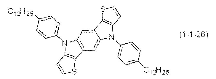 化合物(1−1−26)の物性は以下の通りであった。
1H−NMR(δ、テトラヒドロフラン−d8):0.90(t、6H)、1.23~1.53(m、40H)、2.75(t、4H)、7.11(d、2H)、7.42(d、2H)、7.45(d、4H)、7.62(d、4H)、7.69(s、2H)LC−HRMS(APPI+):calcd for C50H65N2S2、757.4583;found 757.457
[実施例2:化合物(1−1−14)の製造例]
攪拌子、温度計、コンデンサーを取り付けた300mL4つ口フラスコに、化合物(2−2−1) 5.00g(8.96mmol)、トリス(ジベンジリデンアセトン)ジパラジウム(1.64g、1.79mmol)、ラセミ−2,2’−ビス(ジフェニルホスフィノ)−1,1’−ビナフチル(2.23g、3.59mmol)、ドデシルアミン(6.64g、35.85mmol)、ナトリウムtert−ブトキシド(5.17g、53.77mmol)及び脱水トルエン150mlを窒素雰囲気下で仕込み、窒素雰囲気下で還流するまで昇温して同温で8時間攪拌した。得られた反応マスを室温まで冷却した後、水及びトルエンを加えて分液し、得られた有機層を硫酸マグネシウムで乾燥、濾過後、溶媒を減圧下で留去し、固体を得た。得られた固体を、容積比0.2%のトリエチルアミンを添加したヘキサン及びトルエン混合溶媒を用いてシリカゲルクロマトグラフィーにて分離精製し、得られた混合物をヘキサン及びトルエン混合溶媒で再結晶した。得られた結晶を更にリサイクル分取高速液体クロマトグラフィー(移動層;テトラヒドロフラン、アセトニトリル混合溶媒)で精製することで、化合物(1−1−14)(0.67g、1.11mmol)の白黄色結晶を収率12%で得た。
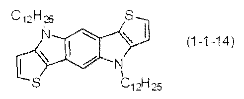 化合物(1−1−14)の物性は以下の通りであった。
1H−NMR(δ、テトラヒドロフラン−d8):0.88(t、6H)、1.20~1.45(m、36H)、1.84~1.98(m、4H)、4.38(t、4H)、7.15(d、2H)、7.38(d、2H)、7.71(s、2H)LC−HRMS(APPI+):calcd for C38H57N2S2、605.3957;found 605.3944
[実施例3:化合物(1)の導電性薄膜を有機半導体層とする有機半導体トランジスタの製造例]
ガラス基板上に、リフトオフプロセスまたはフォトリソグラフィを用いて、クロム、金の順に蒸着して、ソース及びドレイン電極を設置した。この時のクロム層の厚さは5nm、金層の厚さは40nmであった。電極設置後、基板をアセトン、イソプロピルアルコールの順で超音波洗浄を行い、乾燥後、酸素プラズマにてクリーニングを行った後、脱水操作のために80℃で5分間加熱した。この時のチャネル幅は2mm、チャネル長は100μmであった。チャネル部分にフェネチルトリクロロシラン処理を、電極部分にペンタフルオロベンゼンチオール処理を行った後、窒素雰囲気下にて、実施例1で製造した化合物(1−1−26)の0.4wt%のo−キシレン溶液を滴下し、スピンコート法により有機層を、次に有機層の上に、フッ素系ポリマーを含有する溶液を滴下し、スピンコート法により絶縁層を形成した。この時の化合物(1−1−26)の膜厚は25nm、絶縁層の膜厚は300nmであった。絶縁層の上にシャドーマスクを用いて、クロム、アルミニウムの順に蒸着してゲート電極を設置し、図2に示すような有機トランジスタを得た。この時のクロム層の厚さは5nm、アルミニウム層の厚さは200nmであった。
次に、得られた有機トランジスタの電気特性を測定した。化合物(1−1−26)の薄膜を有機半導体層にもつ有機トランジスタは、p型の有機トランジスタであることを確認することができた。さらに、有機トランジスタのキャリアの飽和電界効果移動度μは、有機トランジスタの電気的特性の飽和領域におけるドレイン電流Idを表す式
Id=(W/2L)μCi(Vg−Vt)2 ・・・(a)
を用いて算出した。ここで、L及びWは、それぞれ、有機トランジスタのゲート長及びゲート幅であり、Ciは、ゲート絶縁膜の単位面積当たりの容量であり、Vgは、ゲート電圧であり、Vtは、ゲート電圧のしきい値電圧である。式(a)を用いて、製造した薄膜を有機半導体層にもつ有機トランジスタのキャリア移動度μを計算した結果、キャリア移動度は0.25(cm2/V・s)であった。
なお、反応の進行の確認は高速液体クロマトグラフィー(LC)分析を用いた。
1.高速液体クロマトグラフィー分析
装置 島津LC10AT
カラム 化学物質評価機構製、L−column ODS、内径4.6mm、長さ15cm
リサイクル分取高速液体クロマトグラフィー精製は以下の装置、カラムを用いた。
装置 LC−250HS(日本分析工業社製)
カラム 日本分析工業社製、JAIGEL−ODS−AP−50L、内径50mm、長さ25cm
また、各実施例において生成物の同定は以下の装置により測定によって決定した。
1.1H−NMR:EX270(日本電子株式会社製)
2.LC−HRMS:装置 QSTAR XL(Applied Biosystems社製)カラム 化学物質評価機構製、L−column ODS、内径4.6mm、長さ15cm
[製造例1:1,4−ビス(3−ブロモチオフェン−2−イル)−2,5−ジブロモベンゼン(化合物番号(2−1−1))の製造]
1,4−ビス(3−ブロモチオフェン−2−イル)−2,5−ジブロモベンゼンは、US2011/168953を参考に以下の通り調製した。原料である1,4−ジブロモ−2,5−ジヨードベンゼンは1,4−ジブロモベンゼンをヨウ素と反応させることにより調製した(J.Org.Chem.、1985年、3104頁参照)。
攪拌子、温度計、コンデンサー、滴下ロートを取り付けた1000mL4つ口フラスコに2、3−ジブロモチオフェン(東京化成製、22.3g、92.3mmol)を仕込み、系内を窒素置換し、脱水テトラヒドロフラン240mlを室温(約25℃)にてシリンジを通して加えた。溶液を−78℃まで冷却し、イソプロピルマグネシウムブロミド(東京化成製、1.00M)を含むテトラヒドロフラン溶液(92.3ml、92.3mmol)を同温にて滴下ロートより1時間かけて加え、同温で30分間攪拌した。溶液に塩化亜鉛(アルドリッチ製、1.00M)を含むジエチルエーテル溶液(92.3ml、92.3mmol)を−78℃にて滴下ロートより1時間かけて加え、同温で10分間攪拌した。溶液を室温まで徐々に昇温した後、溶媒を減圧下で留去して白色結晶を得た。この結晶に1,4−ジブロモ−2,5−ジヨードベンゼン(15.0g、30.8mmol)、テトラキストリフェニルホスフィン(東京化成製、3.5g、3.1mmol)を仕込み、系内を窒素置換し、脱水テトラヒドロフラン240mlをシリンジにより加え、還流下、7時間攪拌した。溶液を室温まで冷却し、溶媒を減圧下で除去した。濃縮残渣に10%塩化アンモニウム水溶液(重量比)及びトルエンを加えて分液し、得られたトルエン層を、硫酸マグネシウムで乾燥、濾過後、溶媒を減圧下で留去した。得られた混合物にヘキサンを加えて10分間還流後、室温まで冷却し、混合物を濾過し、濾上物を減圧下で乾燥した。乾燥した濾上物にクロロホルムを加えて10分間還流後、室温まで冷却し、混合物を濾過し、濾上物を減圧下で乾燥することで、1、4−ビス(3−ブロモチオフェン−2−イル)−2、5−ジブロモベンゼン(12.3g、22.0mmol)の白色結晶を1,4−ジブロモ−2,5−ジヨードベンゼンに対する収率71%で得た。その構造式を下記に示す。
1H−NMR(δ、CDCl3):7.09(d、2H)、7.42(d、2H)、7.71(s、2H)
[実施例1:化合物(1−1−26)の製造例]
攪拌子、温度計、コンデンサーを取り付けた500mL4つ口フラスコに化合物(2−2−1) 10.00g(17.92mmol)、トリス(ジベンジリデンアセトン)ジパラジウム(3.28g、3.69mmol)、トリ−tert−ブチルホスフィン(1.45g、7.17mmol)、p−ドデシルアニリン(18.74g、71.69mmol)、ナトリウムtert−ブトキシド(10.33g、107.54mmol)及び脱水トルエン300mlを窒素雰囲気下で仕込み、窒素雰囲気下で80℃に昇温して同温で24時間攪拌した。得られた反応マスを室温まで冷却した後、水及びトルエンを加えて分液し、得られた有機層を硫酸マグネシウムで乾燥、濾過後、溶媒を減圧下で留去し、固体を得た。該固体についてトルエンを用いて再結晶を2回繰り返した後、得られた結晶をテトラヒドロフランに溶解し、該溶解液に活性炭を加え、室温で30分間攪拌した後、濾過した。得られた濾液から溶媒を減圧下で留去し、得られた結晶についてトルエンを用いて再結晶することで、化合物(1−1−26)(4.29g、5.67mmol)の白黄色結晶を収率32%で得た。
1H−NMR(δ、テトラヒドロフラン−d8):0.90(t、6H)、1.23~1.53(m、40H)、2.75(t、4H)、7.11(d、2H)、7.42(d、2H)、7.45(d、4H)、7.62(d、4H)、7.69(s、2H)LC−HRMS(APPI+):calcd for C50H65N2S2、757.4583;found 757.457
[実施例2:化合物(1−1−14)の製造例]
攪拌子、温度計、コンデンサーを取り付けた300mL4つ口フラスコに、化合物(2−2−1) 5.00g(8.96mmol)、トリス(ジベンジリデンアセトン)ジパラジウム(1.64g、1.79mmol)、ラセミ−2,2’−ビス(ジフェニルホスフィノ)−1,1’−ビナフチル(2.23g、3.59mmol)、ドデシルアミン(6.64g、35.85mmol)、ナトリウムtert−ブトキシド(5.17g、53.77mmol)及び脱水トルエン150mlを窒素雰囲気下で仕込み、窒素雰囲気下で還流するまで昇温して同温で8時間攪拌した。得られた反応マスを室温まで冷却した後、水及びトルエンを加えて分液し、得られた有機層を硫酸マグネシウムで乾燥、濾過後、溶媒を減圧下で留去し、固体を得た。得られた固体を、容積比0.2%のトリエチルアミンを添加したヘキサン及びトルエン混合溶媒を用いてシリカゲルクロマトグラフィーにて分離精製し、得られた混合物をヘキサン及びトルエン混合溶媒で再結晶した。得られた結晶を更にリサイクル分取高速液体クロマトグラフィー(移動層;テトラヒドロフラン、アセトニトリル混合溶媒)で精製することで、化合物(1−1−14)(0.67g、1.11mmol)の白黄色結晶を収率12%で得た。
1H−NMR(δ、テトラヒドロフラン−d8):0.88(t、6H)、1.20~1.45(m、36H)、1.84~1.98(m、4H)、4.38(t、4H)、7.15(d、2H)、7.38(d、2H)、7.71(s、2H)LC−HRMS(APPI+):calcd for C38H57N2S2、605.3957;found 605.3944
[実施例3:化合物(1)の導電性薄膜を有機半導体層とする有機半導体トランジスタの製造例]
ガラス基板上に、リフトオフプロセスまたはフォトリソグラフィを用いて、クロム、金の順に蒸着して、ソース及びドレイン電極を設置した。この時のクロム層の厚さは5nm、金層の厚さは40nmであった。電極設置後、基板をアセトン、イソプロピルアルコールの順で超音波洗浄を行い、乾燥後、酸素プラズマにてクリーニングを行った後、脱水操作のために80℃で5分間加熱した。この時のチャネル幅は2mm、チャネル長は100μmであった。チャネル部分にフェネチルトリクロロシラン処理を、電極部分にペンタフルオロベンゼンチオール処理を行った後、窒素雰囲気下にて、実施例1で製造した化合物(1−1−26)の0.4wt%のo−キシレン溶液を滴下し、スピンコート法により有機層を、次に有機層の上に、フッ素系ポリマーを含有する溶液を滴下し、スピンコート法により絶縁層を形成した。この時の化合物(1−1−26)の膜厚は25nm、絶縁層の膜厚は300nmであった。絶縁層の上にシャドーマスクを用いて、クロム、アルミニウムの順に蒸着してゲート電極を設置し、図2に示すような有機トランジスタを得た。この時のクロム層の厚さは5nm、アルミニウム層の厚さは200nmであった。
次に、得られた有機トランジスタの電気特性を測定した。化合物(1−1−26)の薄膜を有機半導体層にもつ有機トランジスタは、p型の有機トランジスタであることを確認することができた。さらに、有機トランジスタのキャリアの飽和電界効果移動度μは、有機トランジスタの電気的特性の飽和領域におけるドレイン電流Idを表す式
Id=(W/2L)μCi(Vg−Vt)2 ・・・(a)
を用いて算出した。ここで、L及びWは、それぞれ、有機トランジスタのゲート長及びゲート幅であり、Ciは、ゲート絶縁膜の単位面積当たりの容量であり、Vgは、ゲート電圧であり、Vtは、ゲート電圧のしきい値電圧である。式(a)を用いて、製造した薄膜を有機半導体層にもつ有機トランジスタのキャリア移動度μを計算した結果、キャリア移動度は0.25(cm2/V・s)であった。
本発明は、キャリア移動度の高い有機半導体デバイス、該デバイスに含まれる薄膜及び該薄膜に含まれる化合物を提供する。
Claims (14)
- 式(1)
(式中、X及びYは、それぞれ独立して、硫黄原子、酸素原子、セレン原子、テルル原子又はSO2を表す。R1~R8は、それぞれ独立して、水素原子、ハロゲン原子、フッ素原子で置換されていてもよい炭素数1~30のアルキル基、フッ素原子で置換されていてもよい炭素数1~30のアルコキシ基、フッ素原子で置換されていてもよい炭素数2~30のアルケニル基、フッ素原子で置換されていてもよい炭素数2~30のアルキニル基、フッ素原子で置換されていてもよい炭素数1~30のアルキルチオ基、炭素数6~30のアリール基又は炭素数4~30のヘテロアリール基を表す。該アリール基及び該ヘテロアリール基には、フッ素原子、フッ素原子で置換されていてもよいアルキル基、フッ素原子で置換されていてもよいアルコキシ基、フッ素原子で置換されていてもよいアルケニル基、フッ素原子で置換されていてもよいアルキニル基及びフッ素原子で置換されていてもよいアルキルチオ基からなる群より選ばれる一以上を有していてもよい。)
で表されるジカルコゲノベンゾジピロール化合物。 - 前記式(1)において、X及びYが硫黄原子である請求項1に記載のジカルコゲノベンゾジピロール化合物。
- 前記式(1)において、R3及びR4が、水素原子又はハロゲン原子であり、R7及びR8が、炭素数1~30のアルキル基、炭素数7~30のアリール基又は炭素数5~30のヘテロアリール基(ここで該アリール基及び該ヘテロアリール基はフッ素原子で置換されていてもよいアルキル基又はフッ素原子で置換されていてもよいアルコキシ基を有する)である請求項1に記載のジカルコゲノベンゾジピロール化合物。
- 前記式(1)において、R5及びR6が水素原子である請求項1に記載のジカルコゲノベンゾジピロール化合物。
- 前記式(1)において、R1~R4が水素原子又はハロゲン原子である請求項1かに記載のジカルコゲノベンゾジピロール化合物。
- 前記式(1)において、R7及びR8がフッ素原子で置換されていてもよいアルキル基を有する炭素数7~26のアリール基である請求項1に記載のジカルコゲノベンゾジピロール化合物。
- 前記式(1)において、R7及びR8がフッ素原子を有していてもよい炭素数1~20のアルキル基である請求項1に記載のジカルコゲノベンゾジピロール化合物。
- 請求項1~7のいずれかに記載のジカルコゲノベンゾジピロール化合物を含む薄膜。
- 請求項1~7のいずれかに記載のジカルコゲノベンゾジピロール化合物からなる薄膜。
- 請求項8に記載の薄膜を含む有機トランジスタ。
- 請求項8に記載の薄膜を含む有機半導体デバイス。
- 式(2)
(式中、X及びYは、それぞれ独立して、硫黄原子、酸素原子、セレン原子、テルル原子又はSO2を表す。R1~R6は、それぞれ独立して、水素原子、ハロゲン原子、フッ素原子で置換されていてもよい炭素数1~30のアルキル基、フッ素原子で置換されていてもよい炭素数1~30のアルコキシ基、フッ素原子で置換されていてもよい炭素数2~30のアルケニル基、フッ素原子で置換されていてもよい炭素数2~30のアルキニル基、フッ素原子で置換されていてもよい炭素数1~30のアルキルチオ基、炭素数6~30のアリール基又は炭素数4~30のヘテロアリール基を表す。該アリール基及び該ヘテロアリール基は、フッ素原子、フッ素原子で置換されていてもよいアルキル基、フッ素原子で置換されていてもよいアルコキシ基、フッ素原子で置換されていてもよいアルケニル基、フッ素原子で置換されていてもよいアルキニル基及びフッ素原子で置換されていてもよいアルキルチオ基からなる群より選ばれる一以上を有していてもよい。R9~R12は、それぞれ独立して、ハロゲン原子を表す。)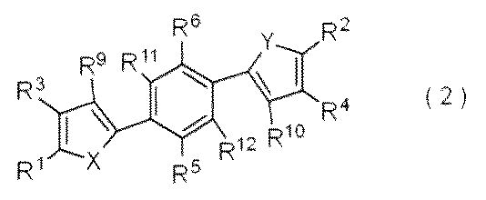
と、式(3)
R7−NH2 (3)
(式中、R7は水素原子、ハロゲン原子、フッ素原子で置換されていてもよい炭素数1~30のアルキル基、フッ素原子で置換されていてもよい炭素数1~30のアルコキシ基、フッ素原子で置換されていてもよい炭素数2~30のアルケニル基、フッ素原子で置換されていてもよい炭素数2~30のアルキニル基、フッ素原子で置換されていてもよい炭素数1~30のアルキルチオ基、炭素数6~30のアリール基又は炭素数4~30のヘテロアリール基を表す。該アリール基及び該ヘテロアリール基は、フッ素原子、フッ素原子で置換されていてもよいアルキル基、フッ素原子で置換されていてもよいアルコキシ基、フッ素原子で置換されていてもよいアルケニル基、フッ素原子で置換されていてもよいアルキニル基及びフッ素原子で置換されていてもよいアルキルチオ基からなる群より選ばれる一以上を有していてもよい。)
で示されるアミン化合物とを反応させる工程を含む式(1’)
(式中、X、Y、R1~R7は前述と同じ。)
で表されるジカルコゲノベンゾジピロール化合物の製造方法。 - 請求項1~7のいずれか記載のジカルコゲノベンゾジピロール化合物及び有機溶媒を含むことを特徴とする組成物。
- 請求項13記載の組成物を基板又は絶縁層上に塗布する工程と、基板又は絶縁層上に塗布された塗布膜を乾燥する工程とを含む薄膜の製造方法。
Priority Applications (1)
| Application Number | Priority Date | Filing Date | Title |
|---|---|---|---|
| US13/981,471 US20130323913A1 (en) | 2011-02-10 | 2012-02-03 | Dichalcogenobenzodipyrrole compound |
Applications Claiming Priority (2)
| Application Number | Priority Date | Filing Date | Title |
|---|---|---|---|
| JP2011-026888 | 2011-02-10 | ||
| JP2011026888A JP5728990B2 (ja) | 2011-02-10 | 2011-02-10 | ジカルコゲノベンゾジピロール化合物、該化合物の製造方法、該化合物を含む薄膜及び該薄膜を含む有機半導体デバイス |
Publications (1)
| Publication Number | Publication Date |
|---|---|
| WO2012108521A1 true WO2012108521A1 (ja) | 2012-08-16 |
Family
ID=46638733
Family Applications (1)
| Application Number | Title | Priority Date | Filing Date |
|---|---|---|---|
| PCT/JP2012/053031 Ceased WO2012108521A1 (ja) | 2011-02-10 | 2012-02-03 | ジカルコゲノベンゾジピロール化合物 |
Country Status (4)
| Country | Link |
|---|---|
| US (1) | US20130323913A1 (ja) |
| JP (1) | JP5728990B2 (ja) |
| TW (1) | TW201240996A (ja) |
| WO (1) | WO2012108521A1 (ja) |
Families Citing this family (11)
| Publication number | Priority date | Publication date | Assignee | Title |
|---|---|---|---|---|
| JP2012188400A (ja) * | 2011-03-11 | 2012-10-04 | Tosoh Corp | ジチエノベンゾジチオフェンの製造方法 |
| JP6079259B2 (ja) * | 2013-01-21 | 2017-02-15 | 東ソー株式会社 | 有機半導体層及び有機薄膜トランジスタ |
| JP6056498B2 (ja) * | 2013-01-21 | 2017-01-11 | 東ソー株式会社 | ジチエノベンゾジフラン誘導体及びその製造方法 |
| JP6252032B2 (ja) * | 2013-08-19 | 2017-12-27 | 東ソー株式会社 | ベンゾジフラン誘導体及び有機薄膜トランジスタ |
| KR102173046B1 (ko) * | 2013-12-06 | 2020-11-03 | 삼성디스플레이 주식회사 | 축합환 화합물 및 이를 포함한 유기 발광 소자 |
| JP6372290B2 (ja) * | 2014-10-07 | 2018-08-15 | 東ソー株式会社 | 1,4−ビス(3−ハロ−2−チエニル)−2,5−ジハロベンゼンの製造方法 |
| JP6363496B2 (ja) * | 2014-12-25 | 2018-07-25 | 富士フイルム株式会社 | 有機半導体インク、有機半導体膜、並びに、有機半導体素子及びその製造方法 |
| CN104766802B (zh) * | 2015-03-26 | 2019-05-03 | 深圳市华星光电技术有限公司 | 液晶显示面板、阵列基板及其薄膜晶体管的制造方法 |
| JP6597087B2 (ja) * | 2015-09-09 | 2019-10-30 | Dic株式会社 | 有機化合物、その製造方法、それを含有する有機半導体材料及びそれを含有する有機トランジスタ |
| WO2019161748A1 (en) * | 2018-02-23 | 2019-08-29 | Peking University | Organic semiconducting compounds |
| DE102019107163B3 (de) * | 2019-03-20 | 2020-09-10 | Fraunhofer-Gesellschaft zur Förderung der angewandten Forschung e.V. | Dünnschichttransistor und Verfahren zum Herstellen eines Dünnschichttransistors |
Citations (3)
| Publication number | Priority date | Publication date | Assignee | Title |
|---|---|---|---|---|
| WO2010000670A1 (en) * | 2008-07-02 | 2010-01-07 | Basf Se | High performance solution processable seminconductor based on dithieno [2,3-d:2',3'-d']benzo[1,2-b:4,5-b'] dithiophene |
| JP2010083884A (ja) * | 2008-09-08 | 2010-04-15 | Sumitomo Chemical Co Ltd | 新規化合物及び有機半導体材料 |
| JP2010138077A (ja) * | 2008-12-09 | 2010-06-24 | Tosoh Corp | ヘテロアセン誘導体及びその用途 |
Family Cites Families (4)
| Publication number | Priority date | Publication date | Assignee | Title |
|---|---|---|---|---|
| US1A (en) * | 1836-07-13 | John Ruggles | Locomotive steam-engine for rail and other roads | |
| US20060125009A1 (en) * | 2004-12-14 | 2006-06-15 | Xerox Corporation | Thin film transistors including indolocarbazoles |
| JP2009224593A (ja) * | 2008-03-17 | 2009-10-01 | Nippon Steel Chem Co Ltd | インドロカルバゾール誘導体を含有する電子デバイス用有機導電性材料 |
| GB2465626B (en) * | 2008-11-28 | 2013-07-31 | Cambridge Display Tech Ltd | Organic semiconductors |
-
2011
- 2011-02-10 JP JP2011026888A patent/JP5728990B2/ja not_active Expired - Fee Related
-
2012
- 2012-02-03 US US13/981,471 patent/US20130323913A1/en not_active Abandoned
- 2012-02-03 WO PCT/JP2012/053031 patent/WO2012108521A1/ja not_active Ceased
- 2012-02-07 TW TW101103894A patent/TW201240996A/zh unknown
Patent Citations (3)
| Publication number | Priority date | Publication date | Assignee | Title |
|---|---|---|---|---|
| WO2010000670A1 (en) * | 2008-07-02 | 2010-01-07 | Basf Se | High performance solution processable seminconductor based on dithieno [2,3-d:2',3'-d']benzo[1,2-b:4,5-b'] dithiophene |
| JP2010083884A (ja) * | 2008-09-08 | 2010-04-15 | Sumitomo Chemical Co Ltd | 新規化合物及び有機半導体材料 |
| JP2010138077A (ja) * | 2008-12-09 | 2010-06-24 | Tosoh Corp | ヘテロアセン誘導体及びその用途 |
Also Published As
| Publication number | Publication date |
|---|---|
| JP2012167031A (ja) | 2012-09-06 |
| TW201240996A (en) | 2012-10-16 |
| US20130323913A1 (en) | 2013-12-05 |
| JP5728990B2 (ja) | 2015-06-03 |
Similar Documents
| Publication | Publication Date | Title |
|---|---|---|
| JP5728990B2 (ja) | ジカルコゲノベンゾジピロール化合物、該化合物の製造方法、該化合物を含む薄膜及び該薄膜を含む有機半導体デバイス | |
| KR20110065511A (ko) | 신규 화합물 및 유기 반도체 재료 | |
| CN103703581B (zh) | 晶体管及其制造方法 | |
| CN103958520B (zh) | 具有半导体特性的化合物及相关组合物和装置 | |
| JP5901732B2 (ja) | 新規複素環式化合物及びその中間体の製造方法並びにその用途 | |
| KR101656763B1 (ko) | 신규한 칼코겐 함유 유기 화합물 및 그 용도 | |
| US8946688B2 (en) | Polycyclic ring-fused compound and organic thin film transistor utilizing the same | |
| JP2010043038A (ja) | ラダー型化合物及び有機半導体材料 | |
| TWI549327B (zh) | 有機場效電晶體及有機半導體材料 | |
| WO2011108765A1 (ja) | 多環式化合物 | |
| KR20130076904A (ko) | [1]벤조티에노[3,2-b][1]벤조티오펜 화합물 및 이의 제조 방법, 및 이를 이용한 유기 전자 소자 | |
| KR20150126898A (ko) | 칼코겐 함유 유기 화합물 및 그의 용도 | |
| JP2011032268A (ja) | 置換ベンゾカルコゲノアセン化合物、該化合物を含有する薄膜及び該薄膜を含有する有機半導体デバイス | |
| KR102079292B1 (ko) | 전자 장치 | |
| KR102090300B1 (ko) | 방향족 복소환 화합물, 그 제조방법, 유기 반도체 재료 및 유기 반도체 디바이스 | |
| JP2015199716A (ja) | 多環縮環化合物、有機半導体材料、有機半導体デバイス及び有機トランジスタ | |
| JP2012206989A (ja) | 可溶性ヘテロアセン化合物及び該化合物を含有する薄膜および有機トランジスタ | |
| JP2012184196A (ja) | 含ピロールヘテロアセン化合物、該化合物の製造方法、該化合物を含む薄膜及び該薄膜を含む有機半導体デバイス | |
| US8613870B2 (en) | Isothioindigo-based polymers | |
| WO2012060460A1 (ja) | 置換カルコゲノアセン化合物 | |
| EP3159334A1 (en) | Intermediates of heteroacene compounds and synthetic method for the preparation of heteroacene compounds using the intermediates | |
| WO2012111533A1 (ja) | 有機トランジスタ用化合物 | |
| KR20220063189A (ko) | 축합 다환 방향족 화합물 | |
| JP2010229048A (ja) | 有機半導体材料 | |
| KR102114805B1 (ko) | 유기 트랜지스터용 유기 반도체 재료 및 유기 트랜지스터 소자 |
Legal Events
| Date | Code | Title | Description |
|---|---|---|---|
| 121 | Ep: the epo has been informed by wipo that ep was designated in this application |
Ref document number: 12744190 Country of ref document: EP Kind code of ref document: A1 |
|
| NENP | Non-entry into the national phase |
Ref country code: DE |
|
| WWE | Wipo information: entry into national phase |
Ref document number: 13981471 Country of ref document: US |
|
| 122 | Ep: pct application non-entry in european phase |
Ref document number: 12744190 Country of ref document: EP Kind code of ref document: A1 |