WO2012105394A1 - 電子部品モジュール、及び該電子部品モジュールを備える多機能カード - Google Patents
電子部品モジュール、及び該電子部品モジュールを備える多機能カード Download PDFInfo
- Publication number
- WO2012105394A1 WO2012105394A1 PCT/JP2012/051593 JP2012051593W WO2012105394A1 WO 2012105394 A1 WO2012105394 A1 WO 2012105394A1 JP 2012051593 W JP2012051593 W JP 2012051593W WO 2012105394 A1 WO2012105394 A1 WO 2012105394A1
- Authority
- WO
- WIPO (PCT)
- Prior art keywords
- electronic component
- partition
- base substrate
- shield film
- component module
- Prior art date
- Legal status (The legal status is an assumption and is not a legal conclusion. Google has not performed a legal analysis and makes no representation as to the accuracy of the status listed.)
- Ceased
Links
Images






Classifications
-
- H—ELECTRICITY
- H05—ELECTRIC TECHNIQUES NOT OTHERWISE PROVIDED FOR
- H05K—PRINTED CIRCUITS; CASINGS OR CONSTRUCTIONAL DETAILS OF ELECTRIC APPARATUS; MANUFACTURE OF ASSEMBLAGES OF ELECTRICAL COMPONENTS
- H05K9/00—Screening of apparatus or components against electric or magnetic fields
- H05K9/0007—Casings
- H05K9/002—Casings with localised screening
- H05K9/0022—Casings with localised screening of components mounted on printed circuit boards [PCB]
- H05K9/0024—Shield cases mounted on a PCB, e.g. cans or caps or conformal shields
- H05K9/0032—Shield cases mounted on a PCB, e.g. cans or caps or conformal shields having multiple parts, e.g. frames mating with lids
-
- H—ELECTRICITY
- H10—SEMICONDUCTOR DEVICES; ELECTRIC SOLID-STATE DEVICES NOT OTHERWISE PROVIDED FOR
- H10W—GENERIC PACKAGES, INTERCONNECTIONS, CONNECTORS OR OTHER CONSTRUCTIONAL DETAILS OF DEVICES COVERED BY CLASS H10
- H10W42/00—Arrangements for protection of devices
- H10W42/20—Arrangements for protection of devices protecting against electromagnetic or particle radiation, e.g. light, X-rays, gamma-rays or electrons
-
- H—ELECTRICITY
- H10—SEMICONDUCTOR DEVICES; ELECTRIC SOLID-STATE DEVICES NOT OTHERWISE PROVIDED FOR
- H10W—GENERIC PACKAGES, INTERCONNECTIONS, CONNECTORS OR OTHER CONSTRUCTIONAL DETAILS OF DEVICES COVERED BY CLASS H10
- H10W42/00—Arrangements for protection of devices
- H10W42/20—Arrangements for protection of devices protecting against electromagnetic or particle radiation, e.g. light, X-rays, gamma-rays or electrons
- H10W42/261—Arrangements for protection of devices protecting against electromagnetic or particle radiation, e.g. light, X-rays, gamma-rays or electrons characterised by their shapes or dispositions
- H10W42/276—Arrangements for protection of devices protecting against electromagnetic or particle radiation, e.g. light, X-rays, gamma-rays or electrons characterised by their shapes or dispositions the arrangements being on an external surface of the package, e.g. on the outer surface of an encapsulation
-
- H—ELECTRICITY
- H05—ELECTRIC TECHNIQUES NOT OTHERWISE PROVIDED FOR
- H05K—PRINTED CIRCUITS; CASINGS OR CONSTRUCTIONAL DETAILS OF ELECTRIC APPARATUS; MANUFACTURE OF ASSEMBLAGES OF ELECTRICAL COMPONENTS
- H05K2201/00—Indexing scheme relating to printed circuits covered by H05K1/00
- H05K2201/10—Details of components or other objects attached to or integrated in a printed circuit board
- H05K2201/10227—Other objects, e.g. metallic pieces
- H05K2201/10371—Shields or metal cases
-
- H—ELECTRICITY
- H10—SEMICONDUCTOR DEVICES; ELECTRIC SOLID-STATE DEVICES NOT OTHERWISE PROVIDED FOR
- H10W—GENERIC PACKAGES, INTERCONNECTIONS, CONNECTORS OR OTHER CONSTRUCTIONAL DETAILS OF DEVICES COVERED BY CLASS H10
- H10W72/00—Interconnections or connectors in packages
- H10W72/851—Dispositions of multiple connectors or interconnections
- H10W72/874—On different surfaces
- H10W72/877—Bump connectors and die-attach connectors
-
- H—ELECTRICITY
- H10—SEMICONDUCTOR DEVICES; ELECTRIC SOLID-STATE DEVICES NOT OTHERWISE PROVIDED FOR
- H10W—GENERIC PACKAGES, INTERCONNECTIONS, CONNECTORS OR OTHER CONSTRUCTIONAL DETAILS OF DEVICES COVERED BY CLASS H10
- H10W90/00—Package configurations
- H10W90/701—Package configurations characterised by the relative positions of pads or connectors relative to package parts
- H10W90/721—Package configurations characterised by the relative positions of pads or connectors relative to package parts of bump connectors
- H10W90/724—Package configurations characterised by the relative positions of pads or connectors relative to package parts of bump connectors between a chip and a stacked insulating package substrate, interposer or RDL
Definitions
- the present invention relates to an electronic component module in which an electronic component is mounted on at least one surface of a base substrate, and a multi-function card including the electronic component module.
- the memory card disclosed in Patent Document 1 includes a first cover, a second cover, a set of lead wires, and a circuit board on which a memory element is mounted.
- the first cover has a pair of openings and forms a space for accommodating the circuit board on which the memory element is mounted by joining the first cover and the second cover.
- One end of the lead wiring is connected to the memory element, and the other end is exposed from the opening and serves as an external terminal.
- the height variation of the memory element mounted on the circuit board, the first cover and the second cover Since it is necessary to consider the accuracy of joining the cover, the bending of the first cover and the second cover itself, etc., between the memory element mounted on the circuit board and the first cover and the second cover. It was necessary to provide a certain gap.
- the present invention has been made in view of such circumstances, and an object thereof is to provide an electronic component module capable of realizing a low-profile shield structure, and a multi-function card including the electronic component module. .
- an electronic component module is bonded to a base substrate, an electronic component mounted on at least one surface of the base substrate, and one surface of the base substrate on which the electronic component is mounted.
- a conductive partition that is bonded to one surface of the base substrate on which the electronic component is mounted and surrounds the electronic component, and a conductive resin layer that contacts the top surface of the electronic component and contacts at least a part of the partition. Therefore, the electronic component mounted on one surface of the base substrate can be reliably shielded by the partition and the shield film. Moreover, since the shield film contacts the top surface of the electronic component surrounded by the partition, the gap between the electronic component and the shield film can be minimized, and a low-profile shield structure is realized. It is possible to provide an electronic component module that can be used.
- the shield film can be deformed according to the height of the electronic component, when the height of the partition is lower than the electronic component having the highest height, the periphery of the shield film is deformed downward. Connected to the partition. Therefore, it is possible to reduce the gap that occurs in the portion where the electronic component having the highest height is not arranged, and to reduce the volume of the entire electronic component module.
- the electronic component module according to the present invention includes the electronic components having different heights, and the shield film is in contact with the top surface of the electronic component having the highest height from the base substrate. It is preferable that the electronic component is in contact with at least a part of the partition at a position lower than the top surface of the highest electronic component.
- the shield film contacts the top surface of the electronic component having the highest height from the base substrate, and the top of the electronic component having the highest height from the base substrate. Since it is in contact with at least a part of the partition at a position lower than the surface, it is possible to reduce the gap generated in the upper part of the electronic component having a low height, and to reduce the volume of the entire electronic component module. In addition, since the corner of the electronic component having the highest height from the base substrate can be covered with the shield film including the conductive resin layer, it is possible to prevent cracks, chips, and the like that are likely to occur at the corner.
- the shield film includes a metal layer, and is formed by laminating a conductive resin layer and a metal layer sequentially from a surface facing the base substrate.
- the shield film includes the metal layer and is formed by laminating the conductive resin layer and the metal layer in order from the surface facing the base substrate. Therefore, the electronic component mounted on one surface of the base substrate is more It becomes possible to shield reliably.
- the shield film further includes an insulating layer, and is formed by laminating a conductive resin layer, a metal layer, and an insulating layer in order from the side facing the base substrate. It is preferable.
- the shield film further includes an insulating layer, and is formed by laminating a conductive resin layer, a metal layer, and an insulating layer in order from the surface facing the base substrate. Electronic components can be shielded more reliably, and the shield film can be insulated and protected.
- the shield film further includes an insulating sheet layer, and the insulating sheet layer is on a surface side facing the base substrate and is in contact with the top surface of the electronic component. It is preferable to be laminated.
- the shield film further includes an insulating sheet layer, and the insulating sheet layer is formed on the surface side facing the base substrate and laminated at a position in contact with the top surface of the electronic component.
- the partition has a shape in which the area of the contact surface with the shield film is larger than that of the joint surface with the base substrate.
- the partition since the partition has a shape in which the area of the contact surface with the shield film is larger than that of the joint surface with the base substrate, the bonding strength between the partition and the shield film can be increased.
- the electronic component module according to the present invention preferably includes a conductive partition that divides one surface of the base substrate on which the electronic component is mounted into a plurality of regions in a region surrounded by the partition. .
- the electronic component may be affected by electromagnetic waves due to the conductive partition that divides one surface of the base substrate on which the electronic component is mounted into a plurality of regions in the region surrounded by the partition. It is possible to shield between the electronic components mounted on one surface of the base substrate by the partition.
- a resin is filled in a region surrounded by the partition.
- the electronic component is mounted on one surface of the base substrate on which the electronic component is mounted outside the region surrounded by the partition.
- the electronic component is mounted on one surface of the base substrate on which the electronic component is mounted outside the area surrounded by the partition, an electronic component that cannot perform a desired function when shielded, for example, a radio wave Even when an electronic component for transmitting and receiving is mounted, the function of transmitting and receiving radio waves without failure can be exhibited, and a multifunctional electronic component module can be provided.
- a multi-function card according to the present invention is characterized by comprising the electronic component module according to the present invention and a housing for housing the electronic component module.
- the conductive partition that is bonded to one surface of the base substrate on which the electronic component is mounted and surrounds the electronic component, and the conductive surface that contacts the top surface of the electronic component and contacts at least a part of the partition. Since the shield film including the resin layer is provided, the electronic component mounted on the one surface of the base substrate can be reliably shielded by the partition and the shield film. Moreover, since the shield film contacts the top surface of the electronic component surrounded by the partition, the gap between the electronic component and the shield film can be minimized, and a low-profile shield structure is realized. It is possible to provide an electronic component module that can be used.
- the shield film can be deformed according to the height of the electronic component, when the height of the partition is lower than the electronic component having the highest height, the periphery of the shield film is deformed downward. Connected to the partition. Therefore, it is possible to reduce the gap that occurs in the portion where the electronic component having the highest height is not arranged, and to reduce the volume of the entire electronic component module.
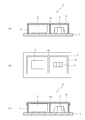
- FIG. 1 is a schematic diagram showing the configuration of the electronic component module according to Embodiment 1 of the present invention.
- FIG. 1A is a schematic diagram showing a configuration of an electronic component module according to Embodiment 1 of the present invention
- FIG. 1B is a shield film of the electronic component module according to Embodiment 1 of the present invention.
- FIG. 1C is a schematic diagram showing a configuration when the shield film of the electronic component module according to Embodiment 1 of the present invention is deformed.
- an electronic component module 10 includes a base substrate 1, electronic components 2 and 3 mounted on at least an upper surface (one surface) of the base substrate 1, an electronic component 2, 3 is bonded to one surface of the base substrate 1 mounted with 3 and surrounds the electronic components 2 and 3.
- the height from the base substrate 1 is A shield film 5 containing a conductive resin is provided which contacts the top surface of the highest electronic component 2 and contacts at least a part of the partition 4.
- the base substrate 1 is not particularly limited to an LTCC (Low Temperature Co-fired Ceramics) substrate, an organic substrate, or the like.
- a surface electrode (not shown) is formed on the surface of the base substrate 1 on which the electronic components 2 and 3 are mounted.
- the electronic component 2 is an integrated circuit (IC) that can be mounted on the base substrate 1.
- the electronic component 3 is a surface mount type electronic component (Surface Mount Device) that can be surface-mounted on the base substrate 1.
- a metal material such as an alloy composed of Cu—Zn—Ni (white) or an alloy composed of Cu—Sn—P (phosphor bronze) can be used. Note that Ni—Sn plating may be applied to an alloy made of Cu—Sn—P.
- the partition 4 processed into a desired shape by pressing, bending, drawing, or the like is joined to the upper surface of the base substrate 1 on which the electronic components 2 and 3 are mounted with solder, conductive resin, or the like. Moreover, it is good also as the partition 4 by arrange
- the partition 4 which has electroconductivity by forming a metal plating film in the member which does not have electroconductivity, such as not only a metal material but processed into the predetermined shape.
- a conductive partition 4 a that partitions the electronic component 2 and the electronic component 3 may be provided in the region surrounded by the partition 4.
- the intermediate partition 4a divides the upper surface of the base substrate 1 into a plurality of regions in a region surrounded by the partition 4 so that the electronic component 2 and the electronic component 3 are not affected by electromagnetic waves. Shielding between 2 and 3.
- the middle partition 4a may not only divide the electronic components 2 and 3 one by one, but may divide the electronic components 2 and 3 by function. .
- one electronic component 2 (3) may exist in one area divided by the partition 4a or the electronic components 2 and 3 may exist depending on the function of the electronic component.
- the partition 4a can be formed by the same method as the partition 4, you may use combining what was formed by the method different from the partition 4. FIG.
- the shield film 5 is formed by laminating a conductive resin layer, a metal layer, and an insulating layer in order from the side in contact with the top surface of the electronic component 2 having the highest height from the base substrate 1, that is, the side facing the base substrate 1. Is formed.
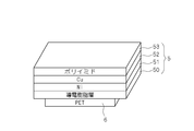
- FIG. 2 is a schematic diagram showing the configuration of the shield film 5 according to Embodiment 1 of the present invention. 2 has a conductive resin layer 50 with a thickness of 20 ⁇ m, a Ni film (metal layer) 51 with a thickness of 0.3 ⁇ m, a Cu film (metal layer) 52 with a thickness of 3.0 ⁇ m, and a thickness of 12.
- the conductive resin layer 50 has heat resistance and has adhesiveness that can be bonded to the electronic component 2, the partition 4, and the like.
- the conductive resin layer 50 is, for example, an epoxy resin containing Ag filler, Cu filler, or the like, a thermosetting resin such as a phenol resin, or a UV curable resin.
- the conductive resin layer 50, the electronic component 2, the partition 4, and the like are temporarily pressure-bonded by, for example, a laminating machine, a press machine, a sealer (sealer), and the like, and the temporarily-bonded conductive resin layer 50 is thermally cured (for example, 150 ° C.
- the conductive resin layer 50 is bonded to the electronic component 2, the partition 4, and the like. Since the conductive resin layer 50 bonds the top surface of the electronic component 2 and the partition 4, it is possible to prevent the positional deviation between the shield film 5 and the electronic component 2. Further, since the conductive resin layer 50 has an adhesive force, the shield film 5 and the partition 4 can be easily mechanically fixed and electrically connected without taking any special connection means. Further, the conductive resin layer 50 may be a conductive adhesive, or a metal layer coated with a conductive adhesive may be used as the shield film 5. Furthermore, the conductive resin layer 50 may be formed using a semi-cured resin sheet (prepreg).
- the shield film 5 includes the conductive resin layer 50 made of a deformable material, the shield film 5 has flexibility before being cured in the manufacturing process, so that the height of the electronic component 2 or the partition 4 is increased. It easily deforms accordingly. Since the shield film 5 includes the metal layers 51 and 52, the metal layers 51 and 52 are electrically connected to the partition 4 through the conductive resin layer 50. Therefore, by bonding the conductive resin layer 50 and the partition 4, the conductive resin layer 50 and the partition 4 are electrically connected, and the electronic components 2 and 3 mounted on the upper surface of the base substrate 1 are connected to the conductive resin layer 50 ( It is possible to reliably shield the shield film 5) and the partition 4.
- the insulating layer 53 functions as a support layer or a reinforcing layer of the shield film 5 and can prevent the conductive resin layer 50 or the metal layers 51 and 52 from being broken. . And since the insulating layer 53 has covered the outer side of the metal layers 51 and 52, it can prevent that the metal layers 51 and 52 and an outside component short-circuit.
- the shield film 5 may be formed only of the conductive resin layer 50.
- the shield film 5 is deformed along the side surface of the partition 4 so as to wrap around a part of the side surface of the partition 4 as shown in FIG. May be.
- the shield film 5 can be made one size larger than the partition 4, even when the shield film 5 is misplaced when the shield film 5 is disposed on the partition 4, the shield film 5. And the partition 4 are not easily connected to each other.
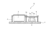
- FIG. 3 is a schematic diagram showing the configuration of the electronic component module according to Embodiment 2 of the present invention. It is embodiment which shows the structure in case the shield film 5 of the electronic component module 10 contacts the several part from which height differs.
- the shield film 5 is in contact with the top surface of the electronic component 2 having the highest height from the base substrate 1, and the height from the base substrate 1 is the highest. It is preferable to contact at least a part of the partition 4 having conductivity at a position lower than the top surface of the high electronic component 2. This is because the corners of the electronic component 2 having the highest height from the base substrate 1 can be covered with the shield film 5, so that cracks, chips and the like that are likely to occur at the corners can be prevented.
- FIG. 3 shows a case where the height of the contact surface of the shield film 5 of the electronic component module 10 with the electronic component 2 is different from the height of the contact surface with the partition 4. As shown in FIG. 3, at least a part of the shield film 5 is in contact with at least a part of the partition 4 at a position lower than the top surface of the electronic component 2 having the highest height from the base substrate 1.
- the shield film 5 includes the conductive resin layer 50 made of a deformable material, the shield film 5 has flexibility in the manufacturing process, and the height of the electronic component 2 and the partition 4 having different heights. Accordingly, the two can be easily connected to each other.
- the conductive resin layer 50 constituting the shield film 5 has elasticity, cracks that are likely to occur at the corners by covering the corners of the electronic component 2 having the highest height from the base substrate 1 with the shield film 5. , Chipping and the like can be prevented.
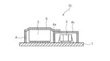
- FIG. 4 is a schematic diagram showing the configuration of the electronic component module according to Embodiment 3 of the present invention. It is embodiment which shows the other structure in the case of contacting the some part from which the height which the shielding film 5 of the electronic component module 10 contacts differs. As shown in FIG. 3, even if the shield film 5 is not in contact with the top surface of the electronic component 3, the height from the base substrate 1 is lower than the height of the electronic component 2 from the base substrate 1. May be.
- the shield film 5 is provided along the top surface of the electronic component 3 having a low height.
- the electrode 3 a reaches the top surface side of the electronic component 3, the electronic component 3 and the shield film 5 are in contact with each other via the insulating sheet 6. It goes without saying that a short circuit can be prevented.
- FIG. 5 is a schematic diagram showing the configuration of the electronic component module according to Embodiment 4 of the present invention.
- the shield film 5 of the electronic component module 10 is provided up to the middle of the lid part beyond the partition 4.
- the shield film 5 may cover the entire region surrounded by the partition 4 or may cover only a part of the region surrounded by the partition 4. For example, you may cover the one part area
- the lid 4c is formed by covering a part of the partition 4 so as to cover the electronic component 3 by pressing, bending, drawing or the like. Since at least a part of the shield film 5 does not come into contact with the outer edge portion of the partition 4, the shield film 5 can be provided only in a portion that needs to be shielded.
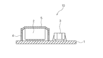
- FIG. 6 is a schematic diagram showing the configuration of the electronic component module according to Embodiment 5 of the present invention.
- the shield film 5 of the electronic component module 10 is provided only in the electronic component 2 that needs to be shielded.
- the shield film 5 may be provided only on the electronic component 2 that needs to be shielded, and may not be provided on the electronic component 3 that does not need to be shielded. As shown in FIG. 6, the shield film 5 is in contact with the top surface of the electronic component 2 having the highest height from the base substrate 1 and is in contact with the outer edge portion of the partition 4 surrounding the electronic component 2. Accordingly, for example, outside the region surrounded by the partition 4, the electronic component 3 that cannot perform a desired function when shielded can be mounted on the upper surface of the base substrate 1, for example, an electronic device that transmits and receives radio waves. Even when the component 3 is mounted, the function of transmitting and receiving radio waves without any obstacle can be exhibited, and the multifunctional electronic component module 10 can be provided.
- FIG. 7 is a schematic diagram showing the configuration of the electronic component module according to Embodiment 6 of the present invention. In this embodiment, a part of the shield film 5 of the electronic component module 10 is in contact with the upper part of the bent portion of the partition 4.
- FIG. 8 is a schematic diagram showing the configuration of the electronic component module according to Embodiment 7 of the present invention. In this embodiment, a part of the shield film 5 of the electronic component module 10 is in contact with the lower part of the bent portion of the partition 4.
- the shield film 5 may be in contact with the upper part of the bent part where a part of the partition 4 is bent, or may be in contact with the lower part. As shown in FIG. 7, the end part (part) of the shield film 5 may be brought into contact with the upper part of the bent part 4b of the partition 4, or as shown in FIG. Part) may be brought into contact with the lower part of the bent portion 4 b of the partition 4. In the configuration shown in FIG. 8, even when a stress such as thermal stress is applied, the end of the shield film 5 brought into contact with the lower portion of the bent portion 4 b of the partition 4 is caught by the bent portion 4 b of the partition 4. The shield film 5 is less likely to be peeled off. In FIG.
- FIG. 9 is a schematic diagram showing a configuration of an electronic component module according to Embodiment 8 of the present invention.
- the electronic components 2 and 3 are mounted outside the area surrounded by the partition 4 of the electronic component module 10. That is, the partition 4a is not always necessary.
- the electronic components 2 and 3 are mounted outside the region surrounded by the partition 4, and the shield film 5 is in contact with the upper part of the bent portion 4 b of the partition 4. 4a is not provided.
- the shield film 5 may be formed in a film shape so as to cover the entire shield portion, or may be formed in a shape such as a mesh shape, a lattice shape, or the like that partially has an opening.
- the Ni film 51 and the Cu film 52 are formed by sequentially stacking Ni foil and Cu foil on the conductive resin layer 50, or by sequentially sputtering Ni and Cu on the conductive resin layer 50. Is configured.
- the metal layer is not limited to the Ni film 51 and the Cu film 52, and may be any conductive material. Further, the metal layer is not limited to the two layers of the Ni film 51 and the Cu film 52, and may be configured by any one of the Ni film 51 and the Cu film 52, or a combination of conductive materials. You may comprise in 3 or more layers.
- the polyimide film 53 is formed by screen-printing polyimide on the Cu film 52 and constitutes an insulating layer.
- the insulating layer is not limited to the polyimide film 53, and may be a solder resist material or an epoxy resin containing silica (SiO 2 ), a solder resist material or an epoxy resin not containing silica. Since the shield film 5 is formed by further laminating a metal layer (Ni film 51 and Cu film 52) and an insulating layer (polyimide film 53) on the conductive resin layer 50, the upper surface of the base substrate 1 is separated by the partition 4 and the shield film 5. Thus, it is possible to reliably shield the electronic components 2 and 3 mounted on the board.
- the electronic component module 10 is bonded to the upper surface of the base substrate 1 on which the electronic components 2 and 3 are mounted, and surrounds the electronic components 2 and 3. Since it has the partition 4 which has, and the shielding film 5 which contacts the top
- the shield film 5 is in contact with the top surface of the electronic component 2 having the highest height from the base substrate 1 among the electronic components 2 and 3 surrounded by the partition 4. Thus, it is possible to provide the electronic component module 10 that can minimize the gap between the electronic component 5 and the low-profile shield structure.
- FIG. 10 is a schematic diagram showing the configuration of the electronic component module 10 according to Embodiment 9 of the present invention.
- 1 is an embodiment showing a configuration when an electronic component module 10 is filled with an insulating resin.
- the shield film 5 covers the entire region surrounded by the partition 4 without providing the partition 4 a, and the region surrounded by the partition 4 is filled with the insulating resin 11.
- the insulating resin is preferably an insulating material such as an epoxy resin containing silica (SiO 2 ) filler.
- the proportion of silica filler is preferably 40 to 90% by weight, for example.
- the filling method of the insulating resin 11 will be described.
- the electronic components 2 and 3 are mounted on the upper surface of the base substrate 1, and a conductive partition 4 is provided to surround the mounted electronic components 2 and 3, and then washed, and the liquid insulating resin 11 is surrounded by the partition 4. Apply in the area. Only the necessary amount is applied and cured so that the liquid insulating resin 11 does not overflow outside the region surrounded by the partition 4. Moreover, you may make it harden
- the insulating resin 11 is not applied to the top surface of the electronic component 2 having the highest height from the base substrate 1. This is because the electronic component module 10 is capable of realizing a low-profile shield structure. Fillet-shaped insulating resin 11 is formed on the side surface of electronic component 2 having the highest height from base substrate 1 due to the surface tension of liquid insulating resin 11. Thereby, since the insulating resin 11 is formed up to the side surface of the electronic component 2, the mechanical strength is improved. By forming the shield film 5 after the insulating resin 11 is cured, the electronic component module 10 in which the insulating resin 11 is filled in the region surrounded by the partition 4 can be manufactured.
- a resin sheet, a solid resin, or the like may be used instead of applying the liquid insulating resin 11 in the region surrounded by the partition 4.
- a resin sheet, solid resin, or the like is placed on the electronic component 2 in the region surrounded by the partition 4.
- the resin amount is adjusted so that the height of the resin sheet, solid resin, or the like does not exceed the height of the electronic component 2 having the highest height from the base substrate 1 after the hot pressing.
- a conductive resin sheet or a conductive paste may be used.
- a conductive paste made of an epoxy resin or a phenol resin containing Ag filler, Ni filler, or the like may be used.
- the shield film 5 includes the conductive resin layer 50, the metal layers 51, 52, in order from the top surface side of the electronic component 2 having the highest height from the base substrate 1, that is, from the surface side facing the base substrate 1. It is not limited to the configuration in which the insulating layer 53 is laminated, but may be only the conductive resin layer, or the configuration in which two layers of the conductive resin layer and the metal layer are laminated, the two layers of the conductive resin layer and the insulating layer. A laminated structure may be used.
- FIG. 11 is a schematic diagram showing a configuration of an electronic component module according to Embodiment 10 of the present invention. It is embodiment which shows a structure in case the shape of the partition 4 of the electronic component module 10 differs.
- the partition 4 In order to increase the bonding strength between the partition 4 and the shield film 5, the partition 4 has a shape in which the area of the contact surface with the shield film 5 is larger than the bonding surface with the upper surface of the base substrate 1. Is preferred.
- the partition 4 has a bent portion 4 b that is a part of the partition 4 on the side that contacts the shield film 5, and a lid portion 4 c that covers the electronic component 3.
- the partition 4 has a larger area on the contact surface with the shield film 5 than the joint surface with the upper surface of the base substrate 1 by the area of the contact surface between the bent portion 4b and the lid portion 4c.
- the bent portion 4b and the lid portion 4c of the partition 4 can be formed by pressing, bending, drawing, or the like.
- the electronic component module 10 has the same configuration as the electronic component module 10 shown in FIG. 1A except that the partition 4 has a bent portion 4b and a lid portion 4c. A detailed description is omitted with reference numerals.
- FIG. 12 is a schematic diagram showing another configuration of the electronic component module according to Embodiment 11 of the present invention.
- the electronic component module 20 includes a base substrate 1, electronic components 2 and 3 mounted on the upper surface (one surface) of the base substrate 1, and a conductive partition 4 and a partition surrounding the electronic components 2 and 3.
- a shield film 5 is provided in contact with the top surface of the electronic component 3 having the highest height from the base substrate 1.
- the electrode 3a reaches the top surface side of the electronic component 3 having the highest height from the base substrate 1, the electronic component module 20 performs an electrical short circuit between the shield film 5 and the electronic component 3.
- the insulating sheet 6 is provided so as to be sandwiched between the shield film 5 and the electronic component 3. Since the electronic component module 20 has the same configuration as the electronic component module 10 shown in FIG. 11 except that the insulating sheet 6 is provided, the same components are denoted by the same reference numerals and detailed description thereof is omitted.
- the insulating sheet 6 can be formed using a resin material that can be used as a solder resist material in addition to a PET resin and an epoxy resin.
- FIG. 13 is a schematic diagram showing the configuration of the shield film 5 and the insulating sheet 6 according to Embodiment 11 of the present invention. 13 includes a conductive resin layer 50 having a thickness of 20 ⁇ m, a Ni film 51 having a thickness of 0.3 ⁇ m, a Cu film 52 having a thickness of 3.0 ⁇ m, and a PI (polyimide) film 53 having a thickness of 12.5 ⁇ m. Are stacked. Further, an insulating sheet 6 of PET resin having a thickness of 15 ⁇ m is attached to the conductive resin layer 50 side of the shield film 5.
- the insulating sheet 6 only needs to have an area enough to cover the top surface of the electronic component 3, and does not need to have the same area as the shield film 5. Therefore, the height of the electronic component module 20 is increased by the thickness of the insulating sheet 6 sandwiched between the shield film 5 and the electronic component 3, but in a region where the insulating sheet 6 is not provided, a low-profile shield is provided.
- the electronic component module 20 capable of realizing the structure can be provided.
- the electrode 3a when the electrode 3a reaches the top surface side of the electronic component 3 having the highest height from the base substrate 1, the shield film Since the insulating sheet 6 is sandwiched between the electronic component 3 and the electronic component 3, a short circuit between the shield film 5 and the electronic component 3 can be prevented.
- FIG. 14 is a schematic diagram showing the configuration of a multi-function card according to Embodiment 12 of the present invention.
- the electronic component modules 10 and 20 according to the first to eleventh embodiments are accommodated in a housing and used as a multifunction card such as an SD memory card or a multimedia card.
- FIG. 14 is a schematic diagram showing the configuration of a multi-function card according to Embodiment 12 of the present invention.
- a multi-function card 100 shown in FIG. 14 includes an electronic component module 30 and a housing (first cover 7 and second cover 8) that accommodates the electronic component module 30.
- the electronic component module 30 includes a base substrate 1, electronic components 2 and 3 mounted on both sides of the base substrate 1, an electronic component 2 and 3 surrounding the electronic component 2 and 3, and an electronic component 2 and 3 surrounded by the partition 4. Among them, a shield film 5 in contact with the top surface of the electronic component 2 having the highest height from the base substrate 1 and an external electrode 9 formed on the lower surface of the base substrate 1 are provided.
- the electronic components 2 and 3 are mounted on both surfaces of the base substrate 1, and the shield film 5 is mounted on the top surface of the electronic component 2 having the highest height from the base substrate 1 mounted on both surfaces of the base substrate 1.
- the same reference numerals are assigned and detailed description is omitted.
- the housing that houses the electronic component module 30 is composed of the first cover 7 and the second cover 8, and is joined to each other to house the electronic component module 30.
- the first cover 7 and the second cover 8 are made of resin, a metal frame coated with resin, or the like.
- an SD memory card has a width of 24 mm, a length of 32 mm, and a thickness of 2.1 mm
- a multimedia card has a width of 24 mm, a length of 32 mm, and a thickness of 1.4 mm.
- the second cover 8 has a shape such that the external electrode 9 formed on the lower surface of the base substrate 1 is exposed. Therefore, the multi-function card 100 can be electrically connected to an external device via the external electrode 9.
- the external electrode 9 is formed by patterning a conductive material on the lower surface of the base substrate 1 and is electrically connected to the electronic components 2 and 3.
- the multifunction card 100 includes the electronic component module 30 including the shield film 5 that contacts the top surface of the electronic component 2 having the highest height from the base substrate 1. Since the housing (the first cover 7 and the second cover 8) that accommodates the electronic component module 30 is provided, the gap between the electronic components 2, 3 and the shield film 5 is minimized and reduced.
- the multi-function card 100 using the electronic component module 30 capable of realizing a back shield structure can be provided.
- FIG. 15 is a schematic diagram showing the configuration of a multi-function card according to Embodiment 13 of the present invention.
- the multifunction card 101 may be mounted with an electronic component that cannot perform a desired function when shielded, for example, an electronic component that transmits and receives radio waves.
- a multi-function card 101 shown in FIG. 15 includes an electronic component module 31 and a housing (first cover 7 and second cover 8) that accommodates the electronic component module 31.
- the electronic component module 31 has the electronic component 3 mounted on the upper surface of the base substrate 1 outside the area surrounded by the conductive partition 4.
- the multi-function card 101 has the same configuration as that of the multi-function card 100 shown in FIG. 14 except that the electronic component module 31 includes the electronic component 3 outside the area surrounded by the partition 4.
- the electronic component 3 since the electronic component 3 is mounted on the upper surface of the base substrate 1 outside the region surrounded by the partition 4, an electronic component that cannot perform a desired function when shielded, for example, Even when the electronic component 3 that transmits and receives radio waves is mounted, the function of transmitting and receiving radio waves without any obstacle can be exhibited.
- the multi-function card is not limited to an SD memory card or a multimedia card, but is particularly limited as long as it is a memory card or IC card that requires a multi-function such as a micro SD card or a SIM card. is not.
- the region surrounded by the partition 4 may be filled with the insulating resin 11.
- the electronic components 2 and 3 may be mounted inside and outside the region surrounded by the partition 4, respectively.
Landscapes
- Engineering & Computer Science (AREA)
- Microelectronics & Electronic Packaging (AREA)
- Shielding Devices Or Components To Electric Or Magnetic Fields (AREA)
Abstract
本発明は、低背なシールド構造を具現化することが可能な電子部品モジュール、及び該電子部品モジュールを備える多機能カードを提供する。 本発明は、ベース基板1と、電子部品2、3と、導電性を有する仕切り4と、シールド膜5とを備える電子部品モジュール10である。電子部品2、3は、ベース基板1の少なくとも一面に実装し、仕切り4は、電子部品2、3を実装したベース基板1の一面に接合され、電子部品2、3を囲む。また、シールド膜5は、電子部品2、3の天面に接触し、仕切り4の少なくとも一部と接触する、導電樹脂層を含む。
Description
本発明は、ベース基板の少なくとも一面に電子部品を実装した電子部品モジュール、及び該電子部品モジュールを備える多機能カードに関する。
近年、携帯電話機、デジタルカメラ等の記憶媒体に、メモリカードが利用されている。特許文献1に開示してあるメモリカードは、第1のカバー、第2のカバー、一組のリード配線、メモリ素子を実装した回路基板を備えている。第1のカバーは、一組の開口部を有し、第1のカバーと第2のカバーとを接合することでメモリ素子を実装した回路基板を収容する空間を形成している。リード配線は、一端がメモリ素子に接続され、他端が開口部から露出して外部端子となっている。
特許文献1に開示してあるメモリカードは、回路基板に実装したメモリ素子をシールドするために、メモリ素子を覆う金属キャップを設ける、又は第1のカバー及び第2のカバーに金属材料を用いることが必要となる。しかし、メモリ素子を覆う金属キャップを設ける場合、回路基板に実装したメモリ素子の高さのバラツキ、金属キャップ自体の高さのバラツキ、金属キャップを回路基板に実装する精度、及び金属キャップ自体の撓み等を考慮する必要があるため、回路基板に実装したメモリ素子とメモリ素子を覆う金属キャップとの間に一定のギャップを設ける必要があった。
また、金属材料を用いた第1のカバー及び第2のカバーで回路基板に実装したメモリ素子をシールドする場合、回路基板に実装したメモリ素子の高さのバラツキ、第1のカバーと第2のカバーとを接合する精度、並びに第1のカバー及び第2のカバー自体の撓み等を考慮する必要があるため、回路基板に実装したメモリ素子と第1のカバー及び第2のカバーとの間に一定のギャップを設ける必要があった。
回路基板に実装したメモリ素子と、金属キャップとの間、第1のカバー及び第2のカバーとの間に一定のギャップを設ける場合、特許文献1に開示してあるメモリカードでは、メモリ素子の高さに加えて一定のギャップを設ける必要があるため、低背化することが困難であるという問題があった。また、金属材料を用いた第1のカバー及び第2のカバーで回路基板の全体をシールドする場合、回路基板に実装したメモリ素子と他の電子部品との間をシールドすることができないという問題があった。
本発明は斯かる事情に鑑みてなされたものであり、低背なシールド構造を具現化することが可能な電子部品モジュール、及び該電子部品モジュールを備える多機能カードを提供することを目的とする。
上記目的を達成するために本発明に係る電子部品モジュールは、ベース基板と、該ベース基板の少なくとも一面に実装した電子部品と、前記電子部品を実装した前記ベース基板の一面に接合され、前記電子部品を囲む、導電性を有する仕切りと、前記電子部品の天面に接触し、前記仕切りの少なくとも一部と接触する、導電樹脂層を含むシールド膜とを備えることを特徴とする。
上記構成では、電子部品を実装したベース基板の一面に接合され、電子部品を囲む、導電性を有する仕切りと、電子部品の天面に接触し、仕切りの少なくとも一部と接触する、導電樹脂層を含むシールド膜とを備えるので、仕切り及びシールド膜でベース基板の一面に実装した電子部品を確実にシールドすることが可能となる。また、シールド膜は、仕切りで囲まれた電子部品の天面に接触するので、電子部品とシールド膜との間のギャップを最小限に抑制することができ、低背なシールド構造を具現化することが可能な電子部品モジュールを提供することができる。また、シールド膜は、電子部品の高さに応じて変形することができるので、仕切りの高さが、高さが最も高い電子部品より低い場合にはシールド膜の周辺部が下方へ変形して仕切りに接続される。そのため、高さが最も高い電子部品が配置されていない部分に生じる空隙部を小さくすることができ、電子部品モジュール全体の体積を小さくすることができる。
また、本発明に係る電子部品モジュールは、高さの異なる前記電子部品を備え、前記シールド膜が、前記ベース基板からの高さが最も高い電子部品の天面に接触し、前記ベース基板からの高さが最も高い電子部品の天面より低い位置で前記仕切りの少なくとも一部と接触されていることが好ましい。
上記構成では、高さの異なる電子部品を備えており、シールド膜が、ベース基板からの高さが最も高い電子部品の天面に接触し、ベース基板からの高さが最も高い電子部品の天面より低い位置で仕切りの少なくとも一部と接触されているので、高さが低い電子部品の上部に生じる空隙部を小さくすることができ、電子部品モジュール全体の体積を小さくすることができる。また、ベース基板からの高さが最も高い電子部品の角部を導電樹脂層を含むシールド膜で覆うことができるので、角部において生じやすいクラック、欠け等を防止することも可能となる。
また、本発明に係る電子部品モジュールは、前記シールド膜は、金属層を含み、前記ベース基板と対向する面側から順に、導電樹脂層、金属層を積層して形成されていることが好ましい。
上記構成では、シールド膜は、金属層を含み、ベース基板と対向する面側から順に、導電樹脂層、金属層を積層して形成されているので、ベース基板の一面に実装した電子部品をより確実にシールドすることが可能となる。
また、本発明に係る電子部品モジュールは、前記シールド膜は、絶縁層をさらに含み、前記ベース基板と対向する面側から順に、導電樹脂層、金属層、絶縁層を積層して形成されていることが好ましい。
上記構成では、シールド膜は、絶縁層をさらに含み、ベース基板と対向する面側から順に、導電樹脂層、金属層、絶縁層を積層して形成されているので、ベース基板の一面に実装した電子部品をより確実にシールドすることができ、シールド膜を絶縁保護することも可能となる。
また、本発明に係る電子部品モジュールは、前記シールド膜は、絶縁シート層をさらに含み、該絶縁シート層は、前記ベース基板と対向する面側であり、前記電子部品の天面に接触する位置に積層して形成されていることが好ましい。
上記構成では、シールド膜は、絶縁シート層をさらに含み、該絶縁シート層は、ベース基板と対向する面側であり、電子部品の天面に接触する位置に積層して形成されているので、電子部品の電極の一部が電子部品の天面に形成されている場合に、シールド膜と電子部品との電気的な短絡を防止することが可能となる。
また、本発明に係る電子部品モジュールは、前記仕切りは、前記ベース基板との接合面より、前記シールド膜との接触面の方が面積が大きくなる形状を有することが好ましい。
上記構成では、仕切りは、ベース基板との接合面より、シールド膜との接触面の方が面積が大きくなる形状を有するので、仕切りとシールド膜との接合強度を強くすることができる。
また、本発明に係る電子部品モジュールは、前記仕切りに囲まれた領域内において、前記電子部品を実装した前記ベース基板の一面を複数の領域に分ける、導電性を有する中仕切りを備えることが好ましい。
上記構成では、仕切りに囲まれた領域内において、電子部品を実装したベース基板の一面を複数の領域に分ける、導電性を有する中仕切りを備えるので、電子部品が互いに電磁波による影響を受けることがないよう、中仕切りによりベース基板の一面に実装した電子部品の間をシールドすることができる。
また、本発明に係る電子部品モジュールは、前記仕切りで囲まれた領域内に樹脂が充填されていることが好ましい。
上記構成では、仕切りで囲まれた領域内に樹脂が充填されているので、ベース基板の一面に実装した電子部品の耐湿性及び機械的強度を向上させることが可能となる。
また、本発明に係る電子部品モジュールは、前記仕切りで囲まれた領域外において、前記電子部品を実装した前記ベース基板の一面に電子部品が実装されていることが好ましい。
上記構成では、仕切りで囲まれた領域外において、電子部品を実装したベース基板の一面に電子部品が実装されているので、シールドした場合に所望の機能を発揮することができない電子部品、例えば電波を送受信する電子部品を実装した場合であっても、障害なく電波を送受信する機能を発揮することができ、多機能な電子部品モジュールを提供することができる。
次に、上記目的を達成するために本発明に係る多機能カードは、上記本発明に係る電子部品モジュールと、該電子部品モジュールを収容する筺体とを備えることを特徴とする。
上記構成では、上記本発明に係る電子部品モジュールと、該電子部品モジュールを収容する筺体とを備えるので、電子部品とシールド膜との間のギャップを最小限に抑制して低背なシールド構造を具現化することが可能な電子部品モジュールを用いた多機能カードを提供することができる。
上記構成によれば、電子部品を実装したベース基板の一面に接合され、電子部品を囲む、導電性を有する仕切りと、電子部品の天面に接触し、仕切りの少なくとも一部と接触する、導電樹脂層を含むシールド膜とを備えるので、仕切り及びシールド膜でベース基板の一面に実装した電子部品を確実にシールドすることが可能となる。また、シールド膜は、仕切りで囲まれた電子部品の天面に接触するので、電子部品とシールド膜との間のギャップを最小限に抑制することができ、低背なシールド構造を具現化することが可能な電子部品モジュールを提供することができる。また、シールド膜は、電子部品の高さに応じて変形することができるので、仕切りの高さが、高さが最も高い電子部品より低い場合にはシールド膜の周辺部が下方へ変形して仕切りに接続される。そのため、高さが最も高い電子部品が配置されていない部分に生じる空隙部を小さくすることができ、電子部品モジュール全体の体積を小さくすることができる。
以下、本発明の実施の形態について、図面を参照しながら詳細に説明する。
(実施の形態1)
図1は、本発明の実施の形態1に係る電子部品モジュールの構成を示す概略図である。図1(a)は、本発明の実施の形態1に係る電子部品モジュールの構成を示す概略図であり、図1(b)は、本発明の実施の形態1に係る電子部品モジュールのシールド膜を除いた状態で平面視した平面図であり、図1(c)は、本発明の実施の形態1に係る電子部品モジュールのシールド膜が変形した場合の構成を示す概略図である。まず、図1(a)及び図1(b)に示すように、電子部品モジュール10は、ベース基板1、ベース基板1の少なくとも上面(一面)に実装した電子部品2、3、電子部品2、3を実装したベース基板1の一面に接合され、電子部品2、3を囲む、導電性を有する仕切り4、仕切り4で囲まれた電子部品2、3のうち、ベース基板1からの高さが最も高い電子部品2の天面に接触し、仕切り4の少なくとも一部と接触する、導電性樹脂を含むシールド膜5を備えている。
図1は、本発明の実施の形態1に係る電子部品モジュールの構成を示す概略図である。図1(a)は、本発明の実施の形態1に係る電子部品モジュールの構成を示す概略図であり、図1(b)は、本発明の実施の形態1に係る電子部品モジュールのシールド膜を除いた状態で平面視した平面図であり、図1(c)は、本発明の実施の形態1に係る電子部品モジュールのシールド膜が変形した場合の構成を示す概略図である。まず、図1(a)及び図1(b)に示すように、電子部品モジュール10は、ベース基板1、ベース基板1の少なくとも上面(一面)に実装した電子部品2、3、電子部品2、3を実装したベース基板1の一面に接合され、電子部品2、3を囲む、導電性を有する仕切り4、仕切り4で囲まれた電子部品2、3のうち、ベース基板1からの高さが最も高い電子部品2の天面に接触し、仕切り4の少なくとも一部と接触する、導電性樹脂を含むシールド膜5を備えている。
ベース基板1としては、LTCC(低温焼成セラミックス:Low Temperature Co-fired Ceramics)基板、有機基板等、特に限定されるものではない。ベース基板1の電子部品2、3を実装する面には、表面電極(図示せず)が形成されている。電子部品2は、ベース基板1に実装することが可能な集積回路(IC)である。また、電子部品3は、ベース基板1に表面実装することが可能な表面実装型電子部品(Surface Mount Device)である。
導電性を有する仕切り4には、Cu-Zn-Niからなる合金(洋白)、Cu-Sn-Pからなる合金(リン青銅)等の金属材料を用いることができる。なお、Cu-Sn-Pからなる合金にNi-Snメッキを施しても良い。プレス加工、折り曲げ加工、絞り加工等により所望の形状に加工された仕切り4は、電子部品2、3を実装したベース基板1の上面に、ハンダ、導電性樹脂等で接合されている。また、複数の金属材料からなるブロックを配置することにより、仕切り4としても良い。金属材料に限らず、所定形状に加工された樹脂等の導電性を有さない部材に金属めっき膜を形成することにより導電性を有する仕切り4としても良い。さらに、仕切り4に囲まれた領域内において、電子部品2と電子部品3との間を仕切る導電性を有する中仕切り4aを設けても良い。中仕切り4aは、電子部品2と電子部品3とが互いに電磁波による影響を受けることがないよう、仕切り4に囲まれた領域内において、ベース基板1の上面を複数の領域に分けて、電子部品2、3の間をシールドしている。中仕切り4aは、図1(a)及び図1(b)に示すように、電子部品2、3を一つずつ区切るだけでなく、電子部品2、3をまとめて機能ごとに区切っても良い。すなわち、電子部品の機能により、中仕切り4aで分けられる一の領域に、1つの電子部品2(3)が存在しても良いし、電子部品2、3が存在しても良い。なお、中仕切り4aは、仕切り4と同様の方法で形成することができるが、仕切り4とは異なる方法により形成されたものを組み合わせて用いても良い。
シールド膜5は、ベース基板1からの高さが最も高い電子部品2の天面に接触する側、すなわちベース基板1と対向する面側から順に、導電樹脂層、金属層、絶縁層を積層して形成されている。図2は、本発明の実施の形態1に係るシールド膜5の構成を示す概略図である。図2に示すシールド膜5は、厚みが20μmの導電樹脂層50、厚みが0.3μmのNi膜(金属層)51、厚みが3.0μmのCu膜(金属層)52、厚みが12.5μmの絶縁層を構成するポリイミド(PI)膜53を積層して形成した導電性樹脂シートである。導電樹脂層50は、耐熱性を有し、電子部品2、仕切り4等と接着することができる粘着性を有している。導電樹脂層50は、例えば、Agフィラ、Cuフィラ等を含有したエポキシ樹脂、フェノール樹脂のような熱硬化性樹脂、又はUV硬化性樹脂等である。導電樹脂層50と電子部品2、仕切り4等とは、例えば、ラミネート機、プレス機、及びシール機(シーラー)等で仮圧着し、仮圧着した導電樹脂層50を熱硬化(例えば、150℃で加熱)して、導電樹脂層50と電子部品2、仕切り4等とを接着する。導電樹脂層50が電子部品2の天面と仕切り4とを接着することにより、シールド膜5と電子部品2との位置ずれを防止することができる。また、導電樹脂層50が接着力を有することで、格別な接続手段を講じることなく、シールド膜5と仕切り4との機械的固定及び電気的接続を容易に行うことができる。また、導電樹脂層50は導電性接着材でも良く、金属層に導電性接着材を塗布したものをシールド膜5として用いても良い。さらには、導電樹脂層50は半硬化樹脂シート(プリプレグ)を用いて形成しても良い。
なお、シールド膜5は、変形することが可能な材料からなる導電樹脂層50を含んでいるため、製造工程において硬化前には可撓性を有するので、電子部品2や仕切り4の高さに応じて容易に変形する。シールド膜5は、金属層51、52を備えているので、金属層51、52が導電樹脂層50を介して仕切り4と電気的に接続される。したがって、導電樹脂層50と仕切り4とを接着することで、導電樹脂層50と仕切り4とが電気的に接続され、ベース基板1の上面に実装した電子部品2、3を導電樹脂層50(シールド膜5)と仕切り4とで確実にシールドすることが可能となる。
さらに、最外層に絶縁層53を設けることにより、絶縁層53が、シールド膜5の支持層又は補強層として機能し、導電樹脂層50又は金属層51、52の破れ等を防止することができる。しかも、絶縁層53が金属層51、52の外側を覆っているので、金属層51、52と外側の部品とが短絡することを防止することができる。もちろん、シールド膜5は導電樹脂層50のみで形成されても良い。
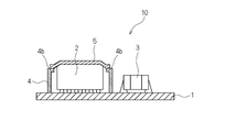
また、シールド層5が容易に変形することから、図1(c)に示すように、シールド膜5が仕切り4の側面に沿って変形して、仕切り4の側面の一部を包みこむように配置されても良い。図1(c)に示す構成とすることで、仕切り4の上面の一部だけでなく、仕切り4の側面の一部でも接着することができ、シールド膜5と仕切り4との接着性をより強固にすることができる。また、シールド膜5を仕切り4よりも一回り大きくすることができるので、仕切り4上にシールド膜5を配置する場合に、シールド膜5の配置ずれが生じたときであっても、シールド膜5と仕切り4とが電気的に接続されないという不具合が生じにくい。
(実施の形態2)
図3は、本発明の実施の形態2に係る電子部品モジュールの構成を示す概略図である。電子部品モジュール10のシールド膜5が、高さが異なる複数の部分に接触する場合の構成を示す実施の形態である。
図3は、本発明の実施の形態2に係る電子部品モジュールの構成を示す概略図である。電子部品モジュール10のシールド膜5が、高さが異なる複数の部分に接触する場合の構成を示す実施の形態である。
高さが異なる電子部品2、3が実装されている場合、シールド膜5は、ベース基板1からの高さが最も高い電子部品2の天面と接触し、ベース基板1からの高さが最も高い電子部品2の天面より低い位置で導電性を有する仕切り4の少なくとも一部と接触することが好ましい。ベース基板1からの高さが最も高い電子部品2の角部をシールド膜5で覆うことができるので、角部において生じやすいクラック、欠け等を防止することができるからである。
図3では、電子部品モジュール10のシールド膜5の、電子部品2との接触面の高さと仕切り4との接触面の高さとが異なる場合を示している。図3に示すように、シールド膜5は、少なくとも一部が、ベース基板1からの高さが最も高い電子部品2の天面より低い位置で仕切り4の少なくとも一部と接触している。
シールド膜5は、変形することが可能な材料からなる導電樹脂層50を含んでいるため、製造工程において可撓性を有しており、高さの異なる電子部品2及び仕切り4の高さに応じて変形し、両者を容易に接続することができる。また、シールド膜5を構成する導電樹脂層50は弾力性を有するため、ベース基板1からの高さが最も高い電子部品2の角部をシールド膜5で覆うことにより、角部において生じやすいクラック、欠け等を防止することができる。
(実施の形態3)
図4は、本発明の実施の形態3に係る電子部品モジュールの構成を示す概略図である。電子部品モジュール10のシールド膜5が接触する高さが異なる複数の部分に接触する場合の他の構成を示す実施の形態である。図3のように、ベース基板1からの高さが電子部品2のベース基板1からの高さに比べて低い電子部品3の天面にシールド膜5が接触していなくても、接触していても良い。
図4は、本発明の実施の形態3に係る電子部品モジュールの構成を示す概略図である。電子部品モジュール10のシールド膜5が接触する高さが異なる複数の部分に接触する場合の他の構成を示す実施の形態である。図3のように、ベース基板1からの高さが電子部品2のベース基板1からの高さに比べて低い電子部品3の天面にシールド膜5が接触していなくても、接触していても良い。
図4では図3とは異なり、高さが低い電子部品3の天面に沿うようにシールド膜5を設けている。もちろん、電子部品3の天面側に電極3aが達している場合には、絶縁シート6を介して電子部品3とシールド膜5とが接触するので、シールド膜5と電子部品3との電気的な短絡を防止することができることは言うまでもない。
(実施の形態4)
図5は、本発明の実施の形態4に係る電子部品モジュールの構成を示す概略図である。電子部品モジュール10のシールド膜5が、仕切り4を越えて蓋部の途中まで設けられている場合の構成を示す実施の形態である。
図5は、本発明の実施の形態4に係る電子部品モジュールの構成を示す概略図である。電子部品モジュール10のシールド膜5が、仕切り4を越えて蓋部の途中まで設けられている場合の構成を示す実施の形態である。
シールド膜5は、仕切り4で囲まれた領域の全てを覆っても良いし、仕切り4で囲まれた領域の一部のみを覆っても良い。例えば、仕切り4(中仕切り4a)で囲まれた一部の領域を覆っていても良い。図5に示すように、シールド膜5は、ベース基板1からの高さが最も高い電子部品2の天面に接触し、高さが低い電子部品3の天面を覆う蓋部4cの途中まで設けられている。蓋部4cは、仕切り4の一部をプレス加工、折り曲げ加工、絞り加工等により、電子部品3を覆うように形成したものである。シールド膜5の少なくとも一部が、仕切り4の外縁部分に接触することがないので、シールドすることが必要な部分のみにシールド膜5を設けることが可能となる。
(実施の形態5)
図6は、本発明の実施の形態5に係る電子部品モジュールの構成を示す概略図である。電子部品モジュール10のシールド膜5が、シールドすることが必要な電子部品2のみに設けられている場合の構成を示す実施の形態である。
図6は、本発明の実施の形態5に係る電子部品モジュールの構成を示す概略図である。電子部品モジュール10のシールド膜5が、シールドすることが必要な電子部品2のみに設けられている場合の構成を示す実施の形態である。
シールド膜5は、シールドすることが必要な電子部品2にのみに設け、シールドする必要のない電子部品3には設けなくても良い。図6に示すように、シールド膜5は、ベース基板1からの高さが最も高い電子部品2の天面に接触し、電子部品2を囲う仕切り4の外縁部分に接触している。これにより、例えば仕切り4で囲まれた領域外において、ベース基板1の上面に、シールドした場合に所望の機能を発揮することができない電子部品3を実装することができ、例えば電波を送受信する電子部品3を実装した場合であっても、障害なく電波を送受信する機能を発揮することができ、多機能な電子部品モジュール10を提供することができる。
(実施の形態6及び7)
図7は、本発明の実施の形態6に係る電子部品モジュールの構成を示す概略図である。電子部品モジュール10のシールド膜5の一部が、仕切り4の折曲部の上部に接触する場合の構成を示す実施の形態である。また、図8は、本発明の実施の形態7に係る電子部品モジュールの構成を示す概略図である。電子部品モジュール10のシールド膜5の一部が、仕切り4の折曲部の下部に接触する場合の構成を示す実施の形態である。
図7は、本発明の実施の形態6に係る電子部品モジュールの構成を示す概略図である。電子部品モジュール10のシールド膜5の一部が、仕切り4の折曲部の上部に接触する場合の構成を示す実施の形態である。また、図8は、本発明の実施の形態7に係る電子部品モジュールの構成を示す概略図である。電子部品モジュール10のシールド膜5の一部が、仕切り4の折曲部の下部に接触する場合の構成を示す実施の形態である。
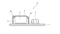
シールド膜5は、仕切り4の一部を折り曲げた折曲部の上部に接触しても良いし、下部に接触しても良い。図7に示すように、シールド膜5の端部(一部)を、仕切り4の折曲部4bの上部に接触させても良いし、図8に示すように、シールド膜5の端部(一部)を、仕切り4の折曲部4bの下部に接触させても良い。図8に示す構成では、熱応力等の応力がかかった場合であっても、仕切り4の折曲部4bの下部に接触させたシールド膜5の端部が仕切り4の折曲部4bに引っ掛かり、シールド膜5が剥離しにくいという効果を奏する。図8では、シールド膜5の端部の一部だけが仕切り4の折曲部4bの下部に接触しているが、特にこれに限定されるものではなく、例えばシールド膜5の端部を、仕切り4の折曲部4bの下部にのみ接触させていても良い。
(実施の形態8)
図9は、本発明の実施の形態8に係る電子部品モジュールの構成を示す概略図である。電子部品モジュール10の仕切り4で囲まれた領域の外に、電子部品2、3が実装されている場合の構成を示す実施の形態である。つまり、中仕切り4aは必ずしも必要ではない。図9に示すように、仕切り4で囲まれた領域の外に電子部品2、3が実装されており、シールド膜5を、仕切り4の折曲部4bの上部に接触させてあり、中仕切り4aを設けていない。シールドすることが必要である電子部品2、3のみを囲む仕切り4を配置し、シールド膜5を形成することにより、電子部品モジュール10において容易に部分的なシールド構造を形成することができる。
図9は、本発明の実施の形態8に係る電子部品モジュールの構成を示す概略図である。電子部品モジュール10の仕切り4で囲まれた領域の外に、電子部品2、3が実装されている場合の構成を示す実施の形態である。つまり、中仕切り4aは必ずしも必要ではない。図9に示すように、仕切り4で囲まれた領域の外に電子部品2、3が実装されており、シールド膜5を、仕切り4の折曲部4bの上部に接触させてあり、中仕切り4aを設けていない。シールドすることが必要である電子部品2、3のみを囲む仕切り4を配置し、シールド膜5を形成することにより、電子部品モジュール10において容易に部分的なシールド構造を形成することができる。
なお、シールド膜5は、シールド部分全面を覆うよう膜状に形成されても良いし、メッシュ状、格子状等、部分的に開口部を有する形状に形成されても良い。
図2に戻って、Ni膜51及びCu膜52は、導電樹脂層50にNi箔及びCu箔を順に積層する、又は導電樹脂層50にNi及びCuを順にスパッタすることで形成され、金属層を構成している。金属層は、Ni膜51及びCu膜52に限定されるものではなく、導電材料であれば良い。また、金属層は、Ni膜51とCu膜52との2層に限定されるものではなく、Ni膜51又はCu膜52のいずれか1層で構成しても良いし、導電材料を組み合わせた3層以上で構成しても良い。ポリイミド膜53は、Cu膜52上にポリイミドをスクリーン印刷することで形成され、絶縁層を構成している。絶縁層は、ポリイミド膜53に限定されるものではなく、シリカ(SiO2 )を含有するソルダーレジスト材又はエポキシ樹脂、シリカを含有しないソルダーレジスト材又はエポキシ樹脂等であっても良い。シールド膜5は、導電樹脂層50に、金属層(Ni膜51及びCu膜52)及び絶縁層(ポリイミド膜53)をさらに積層してあるので、仕切り4及びシールド膜5でベース基板1の上面に実装した電子部品2、3を確実にシールドすることが可能となる。
以上のように、本発明の実施の形態1乃至8に係る電子部品モジュール10は、電子部品2、3を実装したベース基板1の上面に接合され、電子部品2、3を囲む、導電性を有する仕切り4と、仕切り4で囲まれた電子部品2、3のうち、ベース基板1からの高さが最も高い電子部品2の天面に接触するシールド膜5とを備えるので、仕切り4及びシールド膜5でベース基板1の上面に実装した電子部品2、3を確実にシールドすることが可能となる。また、シールド膜5は、仕切り4で囲まれた電子部品2、3のうち、ベース基板1からの高さが最も高い電子部品2の天面に接触するので、電子部品2、3とシールド膜5との間のギャップを最小限に抑制することができ、低背なシールド構造を具現化することが可能な電子部品モジュール10を提供することができる。
(実施の形態9)
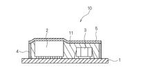
図10は、本発明の実施の形態9に係る電子部品モジュール10の構成を示す概略図である。電子部品モジュール10の絶縁樹脂を充填した場合の構成を示す実施の形態である。図10に示すように、中仕切り4aを設けることなく、シールド膜5が仕切り4で囲まれた領域の全てを覆い、仕切り4で囲まれた領域内に絶縁樹脂11を充填してある。
図10は、本発明の実施の形態9に係る電子部品モジュール10の構成を示す概略図である。電子部品モジュール10の絶縁樹脂を充填した場合の構成を示す実施の形態である。図10に示すように、中仕切り4aを設けることなく、シールド膜5が仕切り4で囲まれた領域の全てを覆い、仕切り4で囲まれた領域内に絶縁樹脂11を充填してある。
絶縁樹脂としては、シリカ(SiO2 )フィラを含有したエポキシ樹脂等の絶縁材であることが好ましい。シリカフィラを含有する割合は、例えば40~90重量%が好ましい。
以下、絶縁樹脂11の充填方法について説明する。まずベース基板1の上面に電子部品2、3を実装し、実装した電子部品2、3を囲む、導電性を有する仕切り4を設けた後、洗浄し、液状の絶縁樹脂11を仕切り4で囲まれた領域内に塗布する。仕切り4で囲まれた領域外に液状の絶縁樹脂11があふれることがないように、必要量のみを塗布して硬化させる。また、必要に応じて真空脱泡した後に硬化させても良い。
なお、ベース基板1からの高さが最も高い電子部品2の天面には絶縁樹脂11は塗布しない。低背なシールド構造を具現化することが可能な電子部品モジュール10にするためである。液状の絶縁樹脂11の表面張力により、ベース基板1からの高さが最も高い電子部品2の側面には、フィレット形状の絶縁樹脂11が形成される。これにより、絶縁樹脂11が電子部品2の側面まで形成されるので機械的強度が向上する。絶縁樹脂11が硬化した後、シールド膜5を形成することで、仕切り4で囲まれた領域内に絶縁樹脂11を充填した電子部品モジュール10を製造することができる。
また、液状の絶縁樹脂11を仕切り4で囲まれた領域内に塗布する代わりに、樹脂シート、固形の樹脂等を用いても良い。この場合、樹脂シート、固形の樹脂等を仕切り4で囲まれた領域内の電子部品2上に載置する。もちろん、樹脂シート、固形の樹脂等の高さが、加熱プレス後、少なくともベース基板1からの高さが最も高い電子部品2の高さを越えないよう樹脂量を調整しておく。
その後、弾性体を介して加熱プレスし、厚み出しを行う。加熱プレス時に弾性体が変形するのに伴って、ベース基板1からの高さが最も高い電子部品2の側面には、フィレット形状の絶縁樹脂11が形成される。これにより、機械的強度が向上する。絶縁樹脂11が硬化した後、シールド膜5を形成することで、仕切り4で囲まれた領域内に絶縁樹脂11を充填した電子部品モジュール10を製造することができる。
シールド膜5は、絶縁樹脂11を充填し、硬化した後に形成する場合には、導電性樹脂シートを用いても良いし、導電性ペーストを用いても良い。例えば、Agフィラ、Niフィラ等を含有するエポキシ樹脂又はフェノール樹脂からなる導電性ペーストを用いれば良い。
また、シールド膜5は、ベース基板1からの高さが最も高い電子部品2の天面側から順に、すなわちベース基板1と対向する面側から順に、導電樹脂層50、金属層51、52、絶縁層53を積層した構成に限定されるものではなく、導電樹脂層のみであっても良いし、導電樹脂層、金属層の2層を積層した構成、導電樹脂層、絶縁層の2層を積層した構成であっても良い。
(実施の形態10)
図11は、本発明の実施の形態10に係る電子部品モジュールの構成を示す概略図である。電子部品モジュール10の仕切り4の形状が異なる場合の構成を示す実施の形態である。仕切り4とシールド膜5との接合強度を強くするためには、仕切り4は、ベース基板1の上面との接合面より、シールド膜5との接触面の方が面積が大きくなる形状にすることが好ましい。図11に示す電子部品モジュール10は、仕切り4が、シールド膜5と接触する側の仕切り4の一部を折り曲げた折曲部4b、電子部品3を覆う蓋部4cを有している。そのため、仕切り4は、折曲部4b及び蓋部4cの接触面の面積分だけ、ベース基板1の上面との接合面より、シールド膜5との接触面の方が面積が大きくなる。仕切り4の折曲部4b及び蓋部4cは、プレス加工、折り曲げ加工、絞り加工等により形成することができる。なお、電子部品モジュール10は、仕切り4が折曲部4b及び蓋部4cを有している以外、図1(a)に示す電子部品モジュール10と同じ構成であるため、同じ構成要素については同じ符号を付して詳細な説明は省略する。
図11は、本発明の実施の形態10に係る電子部品モジュールの構成を示す概略図である。電子部品モジュール10の仕切り4の形状が異なる場合の構成を示す実施の形態である。仕切り4とシールド膜5との接合強度を強くするためには、仕切り4は、ベース基板1の上面との接合面より、シールド膜5との接触面の方が面積が大きくなる形状にすることが好ましい。図11に示す電子部品モジュール10は、仕切り4が、シールド膜5と接触する側の仕切り4の一部を折り曲げた折曲部4b、電子部品3を覆う蓋部4cを有している。そのため、仕切り4は、折曲部4b及び蓋部4cの接触面の面積分だけ、ベース基板1の上面との接合面より、シールド膜5との接触面の方が面積が大きくなる。仕切り4の折曲部4b及び蓋部4cは、プレス加工、折り曲げ加工、絞り加工等により形成することができる。なお、電子部品モジュール10は、仕切り4が折曲部4b及び蓋部4cを有している以外、図1(a)に示す電子部品モジュール10と同じ構成であるため、同じ構成要素については同じ符号を付して詳細な説明は省略する。
(実施の形態11)
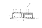
図12は、本発明の実施の形態11に係る電子部品モジュールの他の構成を示す概略図である。図12に示すように、電子部品モジュール20は、ベース基板1、ベース基板1の上面(一面)に実装した電子部品2、3、電子部品2、3を囲む、導電性を有する仕切り4、仕切り4で囲まれた電子部品2、3のうち、ベース基板1からの高さが最も高い電子部品3の天面に接触するシールド膜5を備えている。さらに、電子部品モジュール20は、ベース基板1からの高さが最も高い電子部品3の天面側に電極3aが達している場合には、シールド膜5と電子部品3との電気的な短絡を防止するように、シールド膜5と電子部品3との間に挟むように絶縁シート6を設けている。なお、電子部品モジュール20は、絶縁シート6を設けている以外、図11に示す電子部品モジュール10と同じ構成であるため、同じ構成要素については同じ符号を付して詳細な説明は省略する。
図12は、本発明の実施の形態11に係る電子部品モジュールの他の構成を示す概略図である。図12に示すように、電子部品モジュール20は、ベース基板1、ベース基板1の上面(一面)に実装した電子部品2、3、電子部品2、3を囲む、導電性を有する仕切り4、仕切り4で囲まれた電子部品2、3のうち、ベース基板1からの高さが最も高い電子部品3の天面に接触するシールド膜5を備えている。さらに、電子部品モジュール20は、ベース基板1からの高さが最も高い電子部品3の天面側に電極3aが達している場合には、シールド膜5と電子部品3との電気的な短絡を防止するように、シールド膜5と電子部品3との間に挟むように絶縁シート6を設けている。なお、電子部品モジュール20は、絶縁シート6を設けている以外、図11に示す電子部品モジュール10と同じ構成であるため、同じ構成要素については同じ符号を付して詳細な説明は省略する。
絶縁シート6は、PET樹脂、エポキシ樹脂の他、ソルダーレジスト材として用いることができる樹脂材料を用いて形成することができる。図13は、本発明の実施の形態11に係るシールド膜5及び絶縁シート6の構成を示す概略図である。図13に示すシールド膜5は、厚みが20μmの導電樹脂層50、厚みが0.3μmのNi膜51、厚みが3.0μmのCu膜52、厚みが12.5μmのPI(ポリイミド)膜53を積層してある。さらに、シールド膜5の導電樹脂層50側に、厚みが15μmのPET樹脂の絶縁シート6が張り付けてある。なお、絶縁シート6は、電子部品3の天面を覆う程度の面積を有していれば良く、シールド膜5と同じ面積を有している必要はない。そのため、シールド膜5と電子部品3との間に挟まれた絶縁シート6の厚み分だけ、電子部品モジュール20の高さが高くなるが、絶縁シート6を設けていない領域では、低背なシールド構造を具現化することが可能な電子部品モジュール20を提供することができる。
以上のように、本発明の実施の形態11に係る電子部品モジュール20は、ベース基板1からの高さが最も高い電子部品3の天面側に電極3aが達している場合には、シールド膜5と電子部品3との間に絶縁シート6を挟むようにしてあるので、シールド膜5と電子部品3との短絡を防止することができる。
(実施の形態12)
図14は、本発明の実施の形態12に係る多機能カードの構成を示す概略図である。実施の形態1乃至11に係る電子部品モジュール10、20は、筺体に収容され、例えばSDメモリカード、マルチメディアカード等の多機能カードとして利用される。図14は、本発明の実施の形態12に係る多機能カードの構成を示す概略図である。図14に示す多機能カード100は、電子部品モジュール30、電子部品モジュール30を収容する筺体(第1のカバー7、第2のカバー8)を備えている。
図14は、本発明の実施の形態12に係る多機能カードの構成を示す概略図である。実施の形態1乃至11に係る電子部品モジュール10、20は、筺体に収容され、例えばSDメモリカード、マルチメディアカード等の多機能カードとして利用される。図14は、本発明の実施の形態12に係る多機能カードの構成を示す概略図である。図14に示す多機能カード100は、電子部品モジュール30、電子部品モジュール30を収容する筺体(第1のカバー7、第2のカバー8)を備えている。
電子部品モジュール30は、ベース基板1、ベース基板1の両面に実装した電子部品2、3、電子部品2、3を囲む、導電性を有する仕切り4、仕切り4で囲まれた電子部品2、3のうち、ベース基板1からの高さが最も高い電子部品2の天面に接触するシールド膜5、ベース基板1の下面に形成した外部電極9を備えている。電子部品モジュール30は、ベース基板1の両面に電子部品2、3を実装し、ベース基板1の両面に実装した、ベース基板1からの高さが最も高い電子部品2の天面にシールド膜5が接触している点、及びベース基板1の下面に形成した外部電極9を備えている点以外、図1(a)に示した電子部品モジュール10と同じ構成であるため、同じ構成要素については同じ符号を付して、詳細な説明を省略する。
電子部品モジュール30を収容する筺体は、第1のカバー7と、第2のカバー8とで構成され、互いに接合して電子部品モジュール30を収容する。第1のカバー7及び第2のカバー8は、樹脂、樹脂でコーティングした金属フレーム等で構成されている。筺体は、例えばSDメモリカードであれば幅24mm、長さ32mm、厚さ2.1mmのサイズを有し、マルチメディアカードであれば幅24mm、長さ32mm、厚さ1.4mmのサイズを有する。なお、第2のカバー8は、ベース基板1の下面に形成した外部電極9が露出するような形状を有している。そのため、多機能カード100は、外部電極9を介して外部機器と電気的に接続することができる。外部電極9は、ベース基板1の下面に導電材料をパターニングして形成され、電子部品2、3と電気的に接続されている。
以上のように、本発明の実施の形態12に係る多機能カード100は、ベース基板1からの高さが最も高い電子部品2の天面に接触するシールド膜5を備える電子部品モジュール30と、電子部品モジュール30を収容する筺体(第1のカバー7及び第2のカバー8)とを備えているので、電子部品2、3とシールド膜5との間のギャップを最小限に抑制して低背なシールド構造を具現化することが可能な電子部品モジュール30を用いた多機能カード100を提供することができる。
(実施の形態13)
図15は、本発明の実施の形態13に係る多機能カードの構成を示す概略図である。多機能カード101には、シールドした場合に所望の機能を発揮することができない電子部品、例えば電波を送受信する電子部品を実装することがある。図15に示す多機能カード101は、電子部品モジュール31、電子部品モジュール31を収容する筺体(第1のカバー7及び第2のカバー8)を備えている。電子部品モジュール31は、導電性を有する仕切り4で囲まれた領域外において、ベース基板1の上面に電子部品3を実装してある。多機能カード101は、電子部品モジュール31が仕切り4で囲まれた領域外において電子部品3を備えている点以外、図14に示した多機能カード100と同じ構成であるため、同じ構成要素については同じ符号を付して、詳細な説明を省略する。
図15は、本発明の実施の形態13に係る多機能カードの構成を示す概略図である。多機能カード101には、シールドした場合に所望の機能を発揮することができない電子部品、例えば電波を送受信する電子部品を実装することがある。図15に示す多機能カード101は、電子部品モジュール31、電子部品モジュール31を収容する筺体(第1のカバー7及び第2のカバー8)を備えている。電子部品モジュール31は、導電性を有する仕切り4で囲まれた領域外において、ベース基板1の上面に電子部品3を実装してある。多機能カード101は、電子部品モジュール31が仕切り4で囲まれた領域外において電子部品3を備えている点以外、図14に示した多機能カード100と同じ構成であるため、同じ構成要素については同じ符号を付して、詳細な説明を省略する。
多機能カード101では、電子部品3が、仕切り4で囲まれた領域外において、ベース基板1の上面に実装してあるので、シールドした場合に所望の機能を発揮することができない電子部品、例えば電波を送受信する電子部品3を実装した場合であっても、障害なく電波を送受信するという機能を発揮することができる。
なお、本発明は上記実施例に限定されるものではなく、本発明の趣旨の範囲内であれば多種の変更、改良等が可能である。例えば、多機能カードとして、SDメモリカード、マルチメディアカードに限定されるものではなく、マイクロSDカード、SIMカード等、多機能が要求されるメモリカード、ICカード等であれば特に限定されるものではない。
また、実施の形態11及び12においても、実施の形態9と同様、仕切り4で囲まれた領域内に絶縁樹脂11を充填しても良い。また、実施の形態8と同様、仕切り4で囲まれた領域の内外に、それぞれ電子部品2、3が実装されていても良い。
1 ベース基板
2、3 電子部品
3a 電極
4 仕切り
4a 中仕切り
4b 折曲部
4c 蓋部
5 シールド膜
6 絶縁シート
7 第1のカバー(筺体)
8 第2のカバー(筺体)
9 外部電極
11 絶縁樹脂
50 導電樹脂層
51 Ni膜(金属層)
52 Cu膜(金属層)
53 ポリイミド膜(絶縁層)
10、20、30、31 電子部品モジュール
100、101 多機能カード
2、3 電子部品
3a 電極
4 仕切り
4a 中仕切り
4b 折曲部
4c 蓋部
5 シールド膜
6 絶縁シート
7 第1のカバー(筺体)
8 第2のカバー(筺体)
9 外部電極
11 絶縁樹脂
50 導電樹脂層
51 Ni膜(金属層)
52 Cu膜(金属層)
53 ポリイミド膜(絶縁層)
10、20、30、31 電子部品モジュール
100、101 多機能カード
Claims (10)
- ベース基板と、
該ベース基板の少なくとも一面に実装した電子部品と、
前記電子部品を実装した前記ベース基板の一面に接合され、前記電子部品を囲む、導電性を有する仕切りと、
前記電子部品の天面に接触し、前記仕切りの少なくとも一部と接触する、導電樹脂層を含むシールド膜と
を備えることを特徴とする電子部品モジュール。 - 高さの異なる前記電子部品を備え、
前記シールド膜が、前記ベース基板からの高さが最も高い電子部品の天面に接触し、前記ベース基板からの高さが最も高い電子部品の天面より低い位置で前記仕切りの少なくとも一部と接触されていることを特徴とする請求項1に記載の電子部品モジュール。 - 前記シールド膜は、金属層を含み、前記ベース基板と対向する面側から順に、導電樹脂層、金属層を積層して形成されていることを特徴とする請求項1又は2に記載の電子部品モジュール。
- 前記シールド膜は、絶縁層をさらに含み、前記ベース基板と対向する面側から順に、導電樹脂層、金属層、絶縁層を積層して形成されていることを特徴とする請求項3に記載の電子部品モジュール。
- 前記シールド膜は、絶縁シート層をさらに含み、該絶縁シート層は、前記ベース基板と対向する面側であり、前記電子部品の天面に接触する位置に積層して形成されていることを特徴とする請求項1乃至4のいずれか一項に記載の電子部品モジュール。
- 前記仕切りは、前記ベース基板との接合面より、前記シールド膜との接触面の方が面積が大きくなる形状を有することを特徴とする請求項1乃至5のいずれか一項に記載の電子部品モジュール。
- 前記仕切りに囲まれた領域内において、前記電子部品を実装した前記ベース基板の一面を複数の領域に分ける、導電性を有する中仕切りを備えることを特徴とする請求項1乃至6のいずれか一項に記載の電子部品モジュール。
- 前記仕切りで囲まれた領域内に樹脂が充填されていることを特徴とする請求項1乃至7のいずれか一項に記載の電子部品モジュール。
- 前記仕切りで囲まれた領域外において、前記電子部品を実装した前記ベース基板の一面に電子部品が実装されていることを特徴とする請求項1乃至8のいずれか一項に記載の電子部品モジュール。
- 請求項1乃至9のいずれか一項に記載の電子部品モジュールと、
該電子部品モジュールを収容する筺体と
を備えることを特徴とする多機能カード。
Priority Applications (1)
| Application Number | Priority Date | Filing Date | Title |
|---|---|---|---|
| JP2012555823A JPWO2012105394A1 (ja) | 2011-02-01 | 2012-01-26 | 電子部品モジュール、及び該電子部品モジュールを備える多機能カード |
Applications Claiming Priority (4)
| Application Number | Priority Date | Filing Date | Title |
|---|---|---|---|
| JP2011019910 | 2011-02-01 | ||
| JP2011-019910 | 2011-02-01 | ||
| JP2011099136 | 2011-04-27 | ||
| JP2011-099136 | 2011-04-27 |
Publications (1)
| Publication Number | Publication Date |
|---|---|
| WO2012105394A1 true WO2012105394A1 (ja) | 2012-08-09 |
Family
ID=46602611
Family Applications (1)
| Application Number | Title | Priority Date | Filing Date |
|---|---|---|---|
| PCT/JP2012/051593 Ceased WO2012105394A1 (ja) | 2011-02-01 | 2012-01-26 | 電子部品モジュール、及び該電子部品モジュールを備える多機能カード |
Country Status (2)
| Country | Link |
|---|---|
| JP (1) | JPWO2012105394A1 (ja) |
| WO (1) | WO2012105394A1 (ja) |
Cited By (5)
| Publication number | Priority date | Publication date | Assignee | Title |
|---|---|---|---|---|
| WO2018056239A1 (ja) * | 2016-09-21 | 2018-03-29 | 株式会社村田製作所 | 高周波部品 |
| EP3420786A4 (en) * | 2016-04-29 | 2019-04-03 | Samsung Electronics Co., Ltd. | SHIELDING ELEMENT AND ELECTRONIC DEVICE THEREFOR |
| JP2020174172A (ja) * | 2019-04-05 | 2020-10-22 | サムソン エレクトロ−メカニックス カンパニーリミテッド. | 電子素子モジュール及びその製造方法 |
| WO2022102444A1 (ja) * | 2020-11-10 | 2022-05-19 | 株式会社村田製作所 | 電子部品モジュール、および、電子部品モジュールの製造方法 |
| EP4135500A4 (en) * | 2020-04-30 | 2024-04-03 | Huawei Technologies Co., Ltd. | SHIELDING COVER AND ELECTRONIC DEVICE |
Citations (10)
| Publication number | Priority date | Publication date | Assignee | Title |
|---|---|---|---|---|
| JPH0458596A (ja) * | 1990-06-28 | 1992-02-25 | Nippon Telegr & Teleph Corp <Ntt> | 電磁シールド方法 |
| JPH1126651A (ja) * | 1997-07-04 | 1999-01-29 | Citizen Electron Co Ltd | 電子回路のパッケージ構造 |
| JP2000269632A (ja) * | 1999-03-17 | 2000-09-29 | Tatsuta Electric Wire & Cable Co Ltd | シールドフレキシブルプリント配線板の製造方法、シールドフレキシブルプリント配線板用補強シールドフィルム及びシールドフレキシブルプリント配線板 |
| JP2003133777A (ja) * | 2001-10-24 | 2003-05-09 | Matsushita Electric Ind Co Ltd | シールドケース |
| JP2004047718A (ja) * | 2002-07-11 | 2004-02-12 | Sharp Corp | 高周波電子回路モジュール、および、その製造方法 |
| WO2006059556A1 (ja) * | 2004-12-02 | 2006-06-08 | Murata Manufacturing Co., Ltd. | 電子部品及びその製造方法 |
| JP2007157891A (ja) * | 2005-12-02 | 2007-06-21 | Murata Mfg Co Ltd | 回路モジュールおよびその製造方法 |
| JP2008034713A (ja) * | 2006-07-31 | 2008-02-14 | Fujitsu Ltd | 基板ユニットの製造方法および基板ユニット並びに表面実装用フレームユニット |
| WO2008093559A1 (ja) * | 2007-01-29 | 2008-08-07 | Nec Corporation | 電子機器のシールド構造、シールド部材及びこれを備える電子機器 |
| JP2010103375A (ja) * | 2008-10-24 | 2010-05-06 | Nec Saitama Ltd | シールドカバーの実装構造、シールドカバー、及びシールドフレーム |
-
2012
- 2012-01-26 JP JP2012555823A patent/JPWO2012105394A1/ja active Pending
- 2012-01-26 WO PCT/JP2012/051593 patent/WO2012105394A1/ja not_active Ceased
Patent Citations (10)
| Publication number | Priority date | Publication date | Assignee | Title |
|---|---|---|---|---|
| JPH0458596A (ja) * | 1990-06-28 | 1992-02-25 | Nippon Telegr & Teleph Corp <Ntt> | 電磁シールド方法 |
| JPH1126651A (ja) * | 1997-07-04 | 1999-01-29 | Citizen Electron Co Ltd | 電子回路のパッケージ構造 |
| JP2000269632A (ja) * | 1999-03-17 | 2000-09-29 | Tatsuta Electric Wire & Cable Co Ltd | シールドフレキシブルプリント配線板の製造方法、シールドフレキシブルプリント配線板用補強シールドフィルム及びシールドフレキシブルプリント配線板 |
| JP2003133777A (ja) * | 2001-10-24 | 2003-05-09 | Matsushita Electric Ind Co Ltd | シールドケース |
| JP2004047718A (ja) * | 2002-07-11 | 2004-02-12 | Sharp Corp | 高周波電子回路モジュール、および、その製造方法 |
| WO2006059556A1 (ja) * | 2004-12-02 | 2006-06-08 | Murata Manufacturing Co., Ltd. | 電子部品及びその製造方法 |
| JP2007157891A (ja) * | 2005-12-02 | 2007-06-21 | Murata Mfg Co Ltd | 回路モジュールおよびその製造方法 |
| JP2008034713A (ja) * | 2006-07-31 | 2008-02-14 | Fujitsu Ltd | 基板ユニットの製造方法および基板ユニット並びに表面実装用フレームユニット |
| WO2008093559A1 (ja) * | 2007-01-29 | 2008-08-07 | Nec Corporation | 電子機器のシールド構造、シールド部材及びこれを備える電子機器 |
| JP2010103375A (ja) * | 2008-10-24 | 2010-05-06 | Nec Saitama Ltd | シールドカバーの実装構造、シールドカバー、及びシールドフレーム |
Cited By (9)
| Publication number | Priority date | Publication date | Assignee | Title |
|---|---|---|---|---|
| EP3420786A4 (en) * | 2016-04-29 | 2019-04-03 | Samsung Electronics Co., Ltd. | SHIELDING ELEMENT AND ELECTRONIC DEVICE THEREFOR |
| WO2018056239A1 (ja) * | 2016-09-21 | 2018-03-29 | 株式会社村田製作所 | 高周波部品 |
| JPWO2018056239A1 (ja) * | 2016-09-21 | 2019-07-25 | 株式会社村田製作所 | 高周波部品 |
| US10757845B2 (en) | 2016-09-21 | 2020-08-25 | Murata Manufacturing Co., Ltd. | High-frequency component provided with a shield case |
| JP2020174172A (ja) * | 2019-04-05 | 2020-10-22 | サムソン エレクトロ−メカニックス カンパニーリミテッド. | 電子素子モジュール及びその製造方法 |
| JP7494432B2 (ja) | 2019-04-05 | 2024-06-04 | サムソン エレクトロ-メカニックス カンパニーリミテッド. | 電子素子モジュール及びその製造方法 |
| EP4135500A4 (en) * | 2020-04-30 | 2024-04-03 | Huawei Technologies Co., Ltd. | SHIELDING COVER AND ELECTRONIC DEVICE |
| WO2022102444A1 (ja) * | 2020-11-10 | 2022-05-19 | 株式会社村田製作所 | 電子部品モジュール、および、電子部品モジュールの製造方法 |
| US12243858B2 (en) | 2020-11-10 | 2025-03-04 | Murata Manufacturing Co., Ltd. | Electronic component module, and method of manufacturing electronic component module |
Also Published As
| Publication number | Publication date |
|---|---|
| JPWO2012105394A1 (ja) | 2014-07-03 |
Similar Documents
| Publication | Publication Date | Title |
|---|---|---|
| JP6732932B2 (ja) | 撮像素子実装用基体、撮像装置および撮像モジュール | |
| CN100563405C (zh) | 立体电子电路装置及其中继基板和中继框 | |
| KR101642560B1 (ko) | 전자 소자 모듈 및 그 제조 방법 | |
| JP4186843B2 (ja) | 立体的電子回路装置 | |
| CN103959466B (zh) | 摄像元件收纳用封装及摄像装置 | |
| KR101814546B1 (ko) | 전자 소자 실장용 기판 및 전자 장치 | |
| KR950006439B1 (ko) | 반도체장치 및 그 제조방법 | |
| US10186366B2 (en) | Electrode structure and the corresponding electrical component using the same and the fabrication merhod thereof | |
| JP6107941B2 (ja) | 複合基板 | |
| KR20120023120A (ko) | 반도체 패키지 및 당해 반도체 패키지의 실장구조 | |
| JP4046088B2 (ja) | 立体的電子回路装置およびその中継基板と中継枠 | |
| KR20150000173A (ko) | 전자 소자 모듈 및 그 제조 방법 | |
| CN101971486B (zh) | 半导体器件和具备该半导体器件的通信设备以及电子设备 | |
| WO2012105394A1 (ja) | 電子部品モジュール、及び該電子部品モジュールを備える多機能カード | |
| JP2019040901A (ja) | 回路基板 | |
| JP4945682B2 (ja) | 半導体記憶装置およびその製造方法 | |
| JP2019040902A (ja) | 回路基板 | |
| KR101772490B1 (ko) | 인쇄회로기판 어셈블리 | |
| JP4918391B2 (ja) | 半導体装置 | |
| JP2019129224A (ja) | パッケージおよび電子装置 | |
| CN110832773B (zh) | 电子部件收纳用封装、电子装置以及电子模块 | |
| JP2012156428A (ja) | 電子部品収納用パッケージ、およびそれを備えた電子装置 | |
| JP6940373B2 (ja) | 受光装置 | |
| JP4901439B2 (ja) | 回路装置および回路モジュール | |
| JP4883882B2 (ja) | 電子装置 |
Legal Events
| Date | Code | Title | Description |
|---|---|---|---|
| 121 | Ep: the epo has been informed by wipo that ep was designated in this application |
Ref document number: 12741919 Country of ref document: EP Kind code of ref document: A1 |
|
| ENP | Entry into the national phase |
Ref document number: 2012555823 Country of ref document: JP Kind code of ref document: A |
|
| NENP | Non-entry into the national phase |
Ref country code: DE |
|
| 122 | Ep: pct application non-entry in european phase |
Ref document number: 12741919 Country of ref document: EP Kind code of ref document: A1 |