WO2012081167A1 - 半導体装置及びその製造方法 - Google Patents
半導体装置及びその製造方法 Download PDFInfo
- Publication number
- WO2012081167A1 WO2012081167A1 PCT/JP2011/006416 JP2011006416W WO2012081167A1 WO 2012081167 A1 WO2012081167 A1 WO 2012081167A1 JP 2011006416 W JP2011006416 W JP 2011006416W WO 2012081167 A1 WO2012081167 A1 WO 2012081167A1
- Authority
- WO
- WIPO (PCT)
- Prior art keywords
- substrate
- porous metal
- solder
- semiconductor device
- bonding material
- Prior art date
- Legal status (The legal status is an assumption and is not a legal conclusion. Google has not performed a legal analysis and makes no representation as to the accuracy of the status listed.)
- Ceased
Links
Images



Classifications
-
- H—ELECTRICITY
- H10—SEMICONDUCTOR DEVICES; ELECTRIC SOLID-STATE DEVICES NOT OTHERWISE PROVIDED FOR
- H10W—GENERIC PACKAGES, INTERCONNECTIONS, CONNECTORS OR OTHER CONSTRUCTIONAL DETAILS OF DEVICES COVERED BY CLASS H10
- H10W72/00—Interconnections or connectors in packages
- H10W72/071—Connecting or disconnecting
- H10W72/073—Connecting or disconnecting of die-attach connectors
-
- H—ELECTRICITY
- H10—SEMICONDUCTOR DEVICES; ELECTRIC SOLID-STATE DEVICES NOT OTHERWISE PROVIDED FOR
- H10W—GENERIC PACKAGES, INTERCONNECTIONS, CONNECTORS OR OTHER CONSTRUCTIONAL DETAILS OF DEVICES COVERED BY CLASS H10
- H10W72/00—Interconnections or connectors in packages
- H10W72/01—Manufacture or treatment
- H10W72/013—Manufacture or treatment of die-attach connectors
- H10W72/01351—Changing the shapes of die-attach connectors
- H10W72/01355—Changing the shapes of die-attach connectors by use of masks
-
- H—ELECTRICITY
- H10—SEMICONDUCTOR DEVICES; ELECTRIC SOLID-STATE DEVICES NOT OTHERWISE PROVIDED FOR
- H10W—GENERIC PACKAGES, INTERCONNECTIONS, CONNECTORS OR OTHER CONSTRUCTIONAL DETAILS OF DEVICES COVERED BY CLASS H10
- H10W72/00—Interconnections or connectors in packages
- H10W72/071—Connecting or disconnecting
- H10W72/073—Connecting or disconnecting of die-attach connectors
- H10W72/07321—Aligning
- H10W72/07327—Aligning involving guiding structures, e.g. spacers or supporting members
-
- H—ELECTRICITY
- H10—SEMICONDUCTOR DEVICES; ELECTRIC SOLID-STATE DEVICES NOT OTHERWISE PROVIDED FOR
- H10W—GENERIC PACKAGES, INTERCONNECTIONS, CONNECTORS OR OTHER CONSTRUCTIONAL DETAILS OF DEVICES COVERED BY CLASS H10
- H10W72/00—Interconnections or connectors in packages
- H10W72/071—Connecting or disconnecting
- H10W72/073—Connecting or disconnecting of die-attach connectors
- H10W72/07331—Connecting techniques
- H10W72/07336—Soldering or alloying
-
- H—ELECTRICITY
- H10—SEMICONDUCTOR DEVICES; ELECTRIC SOLID-STATE DEVICES NOT OTHERWISE PROVIDED FOR
- H10W—GENERIC PACKAGES, INTERCONNECTIONS, CONNECTORS OR OTHER CONSTRUCTIONAL DETAILS OF DEVICES COVERED BY CLASS H10
- H10W72/00—Interconnections or connectors in packages
- H10W72/071—Connecting or disconnecting
- H10W72/073—Connecting or disconnecting of die-attach connectors
- H10W72/07341—Controlling the bonding environment, e.g. atmosphere composition or temperature
-
- H—ELECTRICITY
- H10—SEMICONDUCTOR DEVICES; ELECTRIC SOLID-STATE DEVICES NOT OTHERWISE PROVIDED FOR
- H10W—GENERIC PACKAGES, INTERCONNECTIONS, CONNECTORS OR OTHER CONSTRUCTIONAL DETAILS OF DEVICES COVERED BY CLASS H10
- H10W72/00—Interconnections or connectors in packages
- H10W72/071—Connecting or disconnecting
- H10W72/073—Connecting or disconnecting of die-attach connectors
- H10W72/07351—Connecting or disconnecting of die-attach connectors characterised by changes in properties of the die-attach connectors during connecting
- H10W72/07352—Connecting or disconnecting of die-attach connectors characterised by changes in properties of the die-attach connectors during connecting changes in structures or sizes
-
- H—ELECTRICITY
- H10—SEMICONDUCTOR DEVICES; ELECTRIC SOLID-STATE DEVICES NOT OTHERWISE PROVIDED FOR
- H10W—GENERIC PACKAGES, INTERCONNECTIONS, CONNECTORS OR OTHER CONSTRUCTIONAL DETAILS OF DEVICES COVERED BY CLASS H10
- H10W72/00—Interconnections or connectors in packages
- H10W72/071—Connecting or disconnecting
- H10W72/073—Connecting or disconnecting of die-attach connectors
- H10W72/07351—Connecting or disconnecting of die-attach connectors characterised by changes in properties of the die-attach connectors during connecting
- H10W72/07354—Connecting or disconnecting of die-attach connectors characterised by changes in properties of the die-attach connectors during connecting changes in dispositions
-
- H—ELECTRICITY
- H10—SEMICONDUCTOR DEVICES; ELECTRIC SOLID-STATE DEVICES NOT OTHERWISE PROVIDED FOR
- H10W—GENERIC PACKAGES, INTERCONNECTIONS, CONNECTORS OR OTHER CONSTRUCTIONAL DETAILS OF DEVICES COVERED BY CLASS H10
- H10W72/00—Interconnections or connectors in packages
- H10W72/30—Die-attach connectors
- H10W72/321—Structures or relative sizes of die-attach connectors
- H10W72/325—Die-attach connectors having a filler embedded in a matrix
-
- H—ELECTRICITY
- H10—SEMICONDUCTOR DEVICES; ELECTRIC SOLID-STATE DEVICES NOT OTHERWISE PROVIDED FOR
- H10W—GENERIC PACKAGES, INTERCONNECTIONS, CONNECTORS OR OTHER CONSTRUCTIONAL DETAILS OF DEVICES COVERED BY CLASS H10
- H10W72/00—Interconnections or connectors in packages
- H10W72/30—Die-attach connectors
- H10W72/331—Shapes of die-attach connectors
- H10W72/332—Plan-view shape, i.e. in top view
-
- H—ELECTRICITY
- H10—SEMICONDUCTOR DEVICES; ELECTRIC SOLID-STATE DEVICES NOT OTHERWISE PROVIDED FOR
- H10W—GENERIC PACKAGES, INTERCONNECTIONS, CONNECTORS OR OTHER CONSTRUCTIONAL DETAILS OF DEVICES COVERED BY CLASS H10
- H10W72/00—Interconnections or connectors in packages
- H10W72/30—Die-attach connectors
- H10W72/341—Dispositions of die-attach connectors, e.g. layouts
- H10W72/347—Dispositions of multiple die-attach connectors
-
- H—ELECTRICITY
- H10—SEMICONDUCTOR DEVICES; ELECTRIC SOLID-STATE DEVICES NOT OTHERWISE PROVIDED FOR
- H10W—GENERIC PACKAGES, INTERCONNECTIONS, CONNECTORS OR OTHER CONSTRUCTIONAL DETAILS OF DEVICES COVERED BY CLASS H10
- H10W72/00—Interconnections or connectors in packages
- H10W72/30—Die-attach connectors
- H10W72/351—Materials of die-attach connectors
- H10W72/352—Materials of die-attach connectors comprising metals or metalloids, e.g. solders
-
- H—ELECTRICITY
- H10—SEMICONDUCTOR DEVICES; ELECTRIC SOLID-STATE DEVICES NOT OTHERWISE PROVIDED FOR
- H10W—GENERIC PACKAGES, INTERCONNECTIONS, CONNECTORS OR OTHER CONSTRUCTIONAL DETAILS OF DEVICES COVERED BY CLASS H10
- H10W72/00—Interconnections or connectors in packages
- H10W72/50—Bond wires
- H10W72/59—Bond pads specially adapted therefor
-
- H—ELECTRICITY
- H10—SEMICONDUCTOR DEVICES; ELECTRIC SOLID-STATE DEVICES NOT OTHERWISE PROVIDED FOR
- H10W—GENERIC PACKAGES, INTERCONNECTIONS, CONNECTORS OR OTHER CONSTRUCTIONAL DETAILS OF DEVICES COVERED BY CLASS H10
- H10W72/00—Interconnections or connectors in packages
- H10W72/90—Bond pads, in general
- H10W72/921—Structures or relative sizes of bond pads
- H10W72/923—Bond pads having multiple stacked layers
-
- H—ELECTRICITY
- H10—SEMICONDUCTOR DEVICES; ELECTRIC SOLID-STATE DEVICES NOT OTHERWISE PROVIDED FOR
- H10W—GENERIC PACKAGES, INTERCONNECTIONS, CONNECTORS OR OTHER CONSTRUCTIONAL DETAILS OF DEVICES COVERED BY CLASS H10
- H10W72/00—Interconnections or connectors in packages
- H10W72/90—Bond pads, in general
- H10W72/951—Materials of bond pads
- H10W72/952—Materials of bond pads comprising metals or metalloids, e.g. PbSn, Ag or Cu
-
- H—ELECTRICITY
- H10—SEMICONDUCTOR DEVICES; ELECTRIC SOLID-STATE DEVICES NOT OTHERWISE PROVIDED FOR
- H10W—GENERIC PACKAGES, INTERCONNECTIONS, CONNECTORS OR OTHER CONSTRUCTIONAL DETAILS OF DEVICES COVERED BY CLASS H10
- H10W90/00—Package configurations
- H10W90/701—Package configurations characterised by the relative positions of pads or connectors relative to package parts
- H10W90/731—Package configurations characterised by the relative positions of pads or connectors relative to package parts of die-attach connectors
- H10W90/734—Package configurations characterised by the relative positions of pads or connectors relative to package parts of die-attach connectors between a chip and a stacked insulating package substrate, interposer or RDL
-
- H—ELECTRICITY
- H10—SEMICONDUCTOR DEVICES; ELECTRIC SOLID-STATE DEVICES NOT OTHERWISE PROVIDED FOR
- H10W—GENERIC PACKAGES, INTERCONNECTIONS, CONNECTORS OR OTHER CONSTRUCTIONAL DETAILS OF DEVICES COVERED BY CLASS H10
- H10W90/00—Package configurations
- H10W90/701—Package configurations characterised by the relative positions of pads or connectors relative to package parts
- H10W90/731—Package configurations characterised by the relative positions of pads or connectors relative to package parts of die-attach connectors
- H10W90/736—Package configurations characterised by the relative positions of pads or connectors relative to package parts of die-attach connectors between a chip and a stacked lead frame, conducting package substrate or heat sink
Definitions
- the present invention relates to a semiconductor device having a joint using a porous metal and solder.
- Ni ball-containing solder is used in the joint (see Patent Document 1), and a porous metal and solder without voids larger than the pores of the porous metal are used.
- Patent Document 2 it is known that the metal substrate is provided with an uneven shape (see Patent Document 3).
- Patent Document 1 the thickness of the joint is controlled by joining with a sheet-like solder containing Ni balls.
- Patent Document 2 the thickness of the joint is controlled by using a porous metal having no void larger than the pores of the porous metal and solder.
- Patent Document 3 a concavo-convex shape is formed on a metal substrate, and the thickness of the joint is controlled.
- Japanese Patent No. 4302607 JP 2000-349100 A Japanese Patent No. 3853566
- Vehicles that use electricity for power such as hybrid vehicles and electric vehicles, are equipped with inverter modules to control current and achieve high-efficiency driving. Since a relatively large semiconductor element of about 10 mm square for controlling electricity is mounted on the inverter module, the thickness variation of the joint portion tends to increase. Since stress concentrates at the thin joint thickness, the crack growth rate increases.
- Double-sided cooling structure A structure that can be cooled from the front and back surfaces of a feasible element (double-sided cooling structure) has been developed.
- double-sided cooling structure it is necessary to join the front and back of the semiconductor element with a metal substrate such as Cu, Cu alloy, Al, Al alloy, etc. with solder.
- a metal substrate such as Cu, Cu alloy, Al, Al alloy, etc. with solder.
- solder There is a possibility of short-circuiting by protruding outside the part and contacting the other metal substrate. Further, if there is a large difference in the joining thickness, stress concentrates on a thin portion and the crack progress is promoted.
- the semiconductor element and the substrate may be curved, a technique for controlling the thickness of the junction between the curved semiconductor element and the substrate is necessary.
- the substrate is curved, it is difficult to make the thickness of the entire joint portion uniform, so it is important to control the thickness of the end portion in order to suppress the progress of cracks generated from the end portion of the joint portion. .
- An object of the present invention is to provide a highly reliable semiconductor device that can control the thickness of a junction to solve the above-described problems.
- the configuration described in the claims is adopted.
- the present application includes a plurality of means for solving the above-described problems.
- the bonding material for bonding the first and second substrates is composed of a porous metal and solder,
- the peripheral portion exists up to both ends in the thickness direction to adjust the distance between the two substrates, and the central portion does not exist over the entire thickness direction.
- the junction can be controlled to a predetermined thickness regardless of whether the substrate or the semiconductor element is curved.
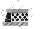
- FIG. It is sectional drawing of the junction part after joining the 1st board
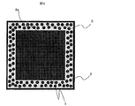
- FIG. It is a top view from the side which joins the 1st substrate 1 after putting porous metal 5 on the 2nd substrate 4 of Example 1 concerning the present invention.
- FIG. 1 is a cross-sectional view of a joint portion after a first substrate 1 and a second substrate 4 are joined using a solder 3 while sandwiching a porous metal 5 in a joining region.
- FIG. 2 is a plan view from the side where the first substrate 1 is joined after the porous metal 5 shown in FIG. 1 is placed on the second substrate 4.
- FIG. 3 is a cross-sectional view of the end portion of the joint portion after the first substrate 1 and the second substrate 4 are joined using the solder 3 while sandwiching the porous metal 5 in the joining region.
- the first substrate 1 is, for example, a semiconductor element, and a power semiconductor element such as a MOS (Metal Oxide Semiconductor), an IGBT (Insulated Gate Bipolar Transistor), a thyristor, or a semiconductor element such as a FWD (Free Wheeling Diode) is considered.
- a power semiconductor element such as a MOS (Metal Oxide Semiconductor), an IGBT (Insulated Gate Bipolar Transistor), a thyristor, or a semiconductor element such as a FWD (Free Wheeling Diode) is considered.
- MOS Metal Oxide Semiconductor
- IGBT Insulated Gate Bipolar Transistor
- a thyristor a semiconductor element such as a FWD (Free Wheeling Diode)
- FWD Free Wheeling Diode
- a conductor layer 2 is formed on the bonding surface side of the first substrate 1.
- the conductor layer 2 has a three-layer structure, and is composed of a lowermost layer, a middle layer, and an uppermost layer from the substrate 1 side. Since the lowermost layer in the conductor layer 2 is in contact with the first substrate, it is formed of Ti in consideration of the adhesive force.
- the thickness of Ti is about 100 nm.
- the middle layer is made of Ni, Ni alloy, Pt, Pt alloy or the like, and has a thickness of about 0.5 ⁇ m to 6 ⁇ m.
- the intermediate layer may be formed of a Cu alloy, an Al alloy, or the like when the substrate 1 is not a semiconductor element such as a ceramic substrate.
- the uppermost layer of the conductor layer 2 is made of Ag, Ag alloy, Au, Au alloy or the like in order to enable solder bonding.
- the thickness of the uppermost layer is about 100 nm to 200 nm.
- the second substrate 4 is a metal substrate such as Cu, Cu alloy, Al, Al alloy or the like, or a ceramic substrate whose main component is one of Al 2 O 3 , AlN, and SiC.
- the second substrate 4 is a metal substrate such as Cu, Cu alloy, Al, Al alloy or the like, it is not always necessary to form a conductor layer on the surface, but in the case of a ceramic substrate, the same as the conductor layer 2 on the bonding surface side It is necessary to form a conductor layer. Since the surface of the conductor layer 2 contains at least one metal of Ag or Ag alloy, which is the uppermost layer, or Au or Au alloy, the first substrate 1 and the second substrate 4 are present. Can be connected by soldering.
- the first substrate 1 and the second substrate 4 are joined with solder 3, and a porous metal 5 is present at a part of the joined portion.
- the porous metal 5 at the joint is impregnated with the solder 3, and all the holes originally possessed by the porous metal are filled with the solder 3.
- solder 3 Sn-based solder containing 90 wt% or more of Sn, or Zn—Al, Zn—Al—Cu solder is used.
- metals such as Cu, Cu alloy, Ni, Ni alloy, Fe, Fe alloy, Al, Al alloy, Mg, Mg alloy, Ti, Ti alloy and the like are used.
- Cu, Cu alloy, Ni, Ni alloy, Ag, Ag alloy, Au, or Au alloy is formed on the outermost surface in contact with the porous metal solder.
- the joint is composed of a central part and a peripheral part around it.
- the porous metal 5 has a cavity 5a larger than the porous hole at the center thereof, and the center of the first substrate 1 is positioned thereon.
- the porous metal 5 exists over the whole of the joining material thickness direction (from one end to the other end). It is supported by solder 3. Since there is no porous metal 5 at the center of the first substrate 1 and the joint, the first substrate is supported by the solder 3 and is located to a position lower than the upper surface of the porous metal 5. That is, even if the first substrate 1 is curved, the porous metal 5 does not exist at the center of the joint, and therefore the thickness of the joint is not affected. For this reason, the position of the 1st board
- the conductor layer 2 to be an electrode is formed on the first substrate 1 by a semiconductor process using a photolithography technique.
- the thickness of the first substrate 1 is, for example, about 0.05 mm to 0.2 mm, and the thickness of the conductor layer 2 formed on the bonding surface side of the first substrate 1 is about 0.5 to 6 ⁇ m. .
- the conductor layer 2 has a laminated structure, and Ti may be formed to a thickness of about 100 nm in a portion in contact with the first substrate 1 in order to improve the adhesion to the first substrate 1.
- the thickness of the second substrate 4 is, for example, about 1 mm to 2 mm. When the second substrate 4 is a metal substrate such as Cu, Cu alloy, Al, Al alloy, etc., it is not always necessary to form a conductor layer on the surface. Absent.
- a frame-like porous metal 5 as shown in FIG. 2 is placed on the second substrate 4. It is placed on a heating plate or the like and heated above the melting point of the solder 3.
- the solder 3 is sucked up from the solder tank containing the molten solder 3 by the piston with the syringe provided with the actuator, and stored in the syringe.
- the syringe is moved within a range where the porous metal 5 is placed, and the solder 3 in the syringe is applied to the frame of the porous metal 5 by the piston.
- a first substrate 1 is placed thereon.
- the coated solder 3 spreads between the first substrate 1 and the second substrate 4.
- the coated solder 3 is impregnated inside the pores of the porous metal 5. Thereafter, the solder is solidified by cooling, and the joining is completed.
- This solder bonding process is preferably performed in an atmosphere filled with an inert gas such as N 2 , a reducing gas such as H 2 , or a mixed gas thereof with an oxygen concentration of 100 ppm or less in order to suppress solder oxidation.
- the thickness of the solder 3 in the joined state is, for example, 50 ⁇ m to 200 ⁇ m.
- the porous metal 5 does not exist in the central portion of the joint portion and is a cavity.
- the present invention is not limited to this, and the central portion of the porous metal 5 is formed to be thinner than the peripheral portion. It is sufficient that it does not exist at either end of the direction.
- the porous metal 5 having the center of the cavity 5a is sandwiched between the joint portions of the first substrate 1 and the second substrate 4, and the vicinity of the center of the porous metal 5 is defined as the cavity 5a. Therefore, even if the substrate is curved, the thickness of the end of the joint can be controlled.
- a metal having a higher thermal conductivity than that of the solder 3 is used for the porous metal 5, thereby increasing the thermal conductivity of the joined portion as compared with the case of joining only with the solder 3. Can do.
- the Young's modulus of the joint can be made equal to that of the solder 3 compared to the case where the same metal as the porous metal 5 is used instead of the porous material.
- the second embodiment is different from the first embodiment in that the porous metal 5 sandwiched between the joint portions of the first substrate 1 and the second substrate 4 is impregnated with the solder 3 in advance.
- the solder sheet 9 containing a porous metal such as that described above is prepared and used for joining. Other points are the same as those of the first embodiment, and the same effects are obtained.
- the conductor layer 2 to be an electrode is formed on the first substrate 1 by a semiconductor process using a photolithography technique.
- the thickness of the first substrate 1 is, for example, about 0.05 mm to 0.2 mm, and the thickness of the conductor layer 2 formed on the bonding surface side of the first substrate 1 is about 0.5 to 6 ⁇ m. .
- the conductor layer 2 has a laminated structure, and Ti may be formed to a thickness of about 100 nm in a portion in contact with the first substrate 1 in order to improve the adhesion to the first substrate 1.
- the thickness of the second substrate 4 is, for example, about 1 mm to 2 mm. When the second substrate 4 is a metal substrate such as Cu, Cu alloy, Al, Al alloy, etc., it is not always necessary to form a conductor layer on the surface. Absent.
- a sheet-like solder 9 including the porous metal 5 as shown in FIG. 4 is placed on the second substrate 4. It is placed on a heating plate or the like, and the first substrate 1 is placed thereon.
- the solder 3 is heated to a melting point or higher. Thereafter, the solder is solidified by cooling, and the joining is completed.
- This solder bonding process is preferably performed in an atmosphere filled with an inert gas such as N 2 , a reducing gas such as H 2 , or a mixed gas thereof with an oxygen concentration of 100 ppm or less in order to suppress solder oxidation.
- the thickness of the solder 3 in the joined state is, for example, 50 ⁇ m to 200 ⁇ m.
- the porous metal 5 Since the porous metal 5 is contained in the solder sheet before joining, the porous metal 5 having a somewhat complicated shape can be used. Therefore, by adopting the second embodiment as described above, the thickness of the bonding portion can be controlled even if the horizontal shape of the first substrate 1 is slightly complicated. In addition, the porous metal 5 having a shape that can easily wet the solder and reduce the void ratio can be easily adopted in accordance with the shape of the substrate.
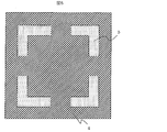
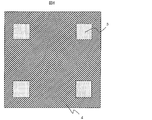
- the third embodiment differs from the first embodiment in that a porous metal 5 having a discontinuous shape is used as shown in FIGS. It is.
- the formation process of the semiconductor device according to this example is the same as that of Example 1 and Example 2.
- the third embodiment By adopting the third embodiment as described above, voids are easily discharged to the outside of the joint during joining.
- the thickness of the joint can be controlled according to the bending state of the first substrate.
- the front and back surfaces of the first substrate, the second substrate 4 and the third substrate 7 are joined by using the solder 3 and sandwiching the porous metal 5 therebetween.
- the solder 3 is preferable to use the same material as the second substrate 4 for the third substrate 7, it is not always necessary to use the same material.
- the heat dissipation of the semiconductor device can be improved, and the semiconductor device can be downsized and the energy density can be increased.
Landscapes
- Die Bonding (AREA)
- Cooling Or The Like Of Semiconductors Or Solid State Devices (AREA)
Abstract
第1の基板1と接合する第2の基板4の一部が湾曲していても接合部の厚さを制御でき、高信頼な半導体装置を提供することを目的とする。 本発明では、第1及び第2の基板を接合する接合材は、多孔質金属とはんだで構成し、この多孔質金属は、周辺部では厚さ方向の両端まで存在して両基板間の間隔を調整するとともに、中心部では、厚さ方向全般にわたっては存在せず、基板の湾曲による設計誤差を中心部のはんだで吸収できるようにした。
Description
本発明は、多孔質金属とはんだを用いた接合部を有する半導体装置に関する。
従来の接合部の厚さ制御としては、接合部にNiボール入りのはんだが用いられている(特許文献1参照)、多孔質金属の空孔より大きな空隙のない多孔質金属とはんだが用いられている(特許文献2参照)、金属基板に凹凸形状を設けている(特許文献3参照)ことが知られている。特許文献1は、Niボール入りのシート状のはんだで接合することで、接合部の厚さを制御している。特許文献2は、多孔質金属の空孔より大きな空隙のない多孔質金属とはんだを用いて接合部の厚さを制御している。特許文献3は、金属基板上に凹凸形状を形成し、接合部の厚さを制御している。
ハイブリッド自動車および電気自動車など、動力に電気を使う車両には、電流を制御し高効率な走行を実現するためにインバーターモジュールが搭載されている。インバーターモジュールには、電気を制御するための10mm角程度の比較的大きな半導体素子が搭載されているため、接合部の厚さバラつきが大きくなりやすい。接合厚の薄い箇所には応力が集中するため、クラック進展速度が大きくなる。
インバーターモジュールの更なる小型化・ハイパワー化が求められており、ハイパワー化すると素子から多くの熱が放出されるため、高放熱なモジュール構造が必要で、モジュールの小型化・ハイパワー化を実現可能な素子の表裏面から冷却可能な構造(両面冷却構造)が開発されている。両面冷却構造では、半導体素子の表裏をCu、Cu合金、Al、Al合金等の金属基板とはんだで接合する必要があり、接合部の厚さばらつきが大きいと接合厚の薄い箇所ではんだが接合部の外にはみ出し、他方の金属基板と接することで短絡する可能性がある。また、接合厚に大きな差があると、薄い箇所に応力が集中し、クラック進展が促進される。
そこで、接合部の厚さを制御できる技術が求められている。ただし、半導体素子や基板は湾曲していることがあるため、湾曲した半導体素子および基板の接合部の厚さを制御する技術が必要である。基板が湾曲している場合接合部全域の厚さを均一にすることは困難なので、接合部の端部から生じるクラックの進展を抑制するために端部の厚さを制御することが重要になる。
本発明の目的は、上記課題を解決すべく、接合部の厚さを制御でき、高信頼な半導体装置を提供することにある。
上記目的を達成するために、例えば特許請求の範囲に記載の構成を採用する。本願は上記課題を解決する手段を複数含んでいるが、その一例を挙げるならば、第1及び第2の基板を接合する接合材は、多孔質金属とはんだで構成し、この多孔質金属は、周辺部では厚さ方向の両端まで存在して両基板間の間隔を調整するとともに、、中心部では、厚さ方向全体にわたっては存在しないようにする。
本発明によれば、基板や半導体素子が湾曲しているかどうかにかかわらず、接合部を所定の厚さに制御することができる。
以下に実施例を用いて本発明の内容を詳細に説明する。
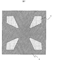
本発明に係る第1の実施の形態について、図1乃至図3を用いて説明する。図1は、第1の基板1と第2の基板4を、接合する領域に多孔質金属5を挟持してはんだ3を使って接合した後の接合部の断面図である。図2は、第2の基板4の上に図1記載の多孔質金属5を置いた後の第1の基板1を接合する側からの平面図である。図3は第1の基板1と第2の基板4を、接合する領域に多孔質金属5を挟持してはんだ3を使って接合した後の接合部端部の断面図である。第1の基板1は、例えば半導体素子であり、MOS(Metal Oxide Semiconductor)やIGBT(Insulated Gate Bipolar Transistor)、サイリスタ等のパワー半導体素子や、若しくはFWD(Free Wheeling Diode)等の半導体素子が考えられる。半導体素子は、例えば厚さ0.1mmから0.2mm程度の薄板状であり、湾曲しており完全な水平基板ではないことが多い。
第1の基板1の接合面側には導体層2が形成されている。導体層2は、3層構造となっており、基板1側から最下層、中層、最上層で構成されている。導体層2における最下層は第1の基板と接触するので、接着力を考慮してTiによって形成される。Tiの厚さは約100nmである。中層は、Ni、Ni合金、Pt、Pt合金等によって形成され、厚さは約0・5μmから6μmである。なお、中層は、基板1がセラミック基板等、半導体素子ではない場合、Cu合金、Al合金等によって形成される場合もある。導体層2の最上層は、はんだ接合を可能とするために、Ag、Ag合金、Au、Au合金等が使用される。最上層の厚さは約100nm~200nmの厚さである。
第2の基板4は、Cu、Cu合金、Al、Al合金等の金属基板、若しくはAl2O3、AlN、SiCのいずれかが主成分のセラミック基板である。第2の基板4がCu、Cu合金、Al、Al合金等の金属基板の場合、必ずしも表面に導体層を形成する必要はないが、セラミック基板の場合、接合面側に導体層2と同様の導体層を形成する必要がある。導体層2の表面は、最上層であるAgもしくはAg合金、またはAuもしくはAu合金のうち少なくとも1種以上の金属が存在していることになるので、第1の基板1と第2の基板4をはんだによって接続することが出来る。
第1の基板1と第2の基板4は、はんだ3で接合されており、その接合部の一部には、多孔質金属5が存在している。接合部の多孔質金属5には、はんだ3が含浸され、多孔質金属が元々有する孔は全てはんだ3で充填されている。はんだ3には、Snを90wt%以上含有しているSn系はんだ、若しくはZn-Al、Zn-Al-Cuのはんだが使用される。多孔質金属5には、Cu、Cu合金、Ni、Ni合金、Fe、Fe合金、Al、Al合金、Mg、Mg合金、Ti、Ti合金等の金属が使用される。多孔質金属のはんだと接する面の最表面には、Cu、Cu合金、Ni、Ni合金、Ag、Ag合金、若しくはAu、Au合金が形成されている。
接合部は、中心部とその周囲の周辺部で構成される。多孔質金属5は、その中心部に、多孔質の孔よりも大きな空洞5aを有しており、その上に第1の基板1の中心部が位置している。第1の基板及び接合部の周辺部において、多孔質金属5は、接合材厚さ方向の全体(一端から他端まで)にわたって存在しており、第1の基板1は、多孔質金属5及びはんだ3で支持されている。第1の基板1及び接合部の中心部では多孔質金属5が無いため、第1の基板ははんだ3で支持されており、多孔質金属5の上面よりも低い位置まで位置している。すなわち、第1の基板1が湾曲しても、接合部の中心部には多孔質金属5が存在していないため、接合部の厚さには影響を与えない。このため、周辺部における多孔質金属5の厚さに基づいて、第1の基板1の位置及び接合部の厚さが決定される。
次に、本実施例に係る半導体装置の形成プロセスの概略について説明する。まず、第1の基板1に電極となる導体層2をフォトリソグラフィー技術を用いた半導体プロセスにより形成する。
第1の基板1の厚さは例えば、0.05mmから0.2mm程度であり、第1の基板1の接合面側に形成された導体層2の厚さは約0・5~6μmである。導体層2は、積層構造として、第1の基板1と接触する部分には、第1の基板1との接着性を向上させるために、Tiが100nm程度形成される場合もある。第2の基板4の厚さは例えば、1mmから2mm程度であり、第2の基板4がCu、Cu合金、Al、Al合金等の金属基板の場合、必ずしも表面に導体層を形成する必要はない。
次に、例えば図2のような枠状の多孔質金属5を第2の基板4上に置く。それを加熱プレートなどの上に配置し、はんだ3の融点以上に加熱しておく。次に、アクチュエータが備わったシリンジでピストンにより、溶融状態のはんだ3が入ったはんだ槽からはんだ3が吸い上げられ、シリンジ内に貯えられる。次に、多孔質金属5を乗せた範囲内にシリンジが移動され、ピストンによりシリンジ内のはんだ3が多孔質金属5の枠内に塗出される。その上から第1の基板1を乗せる。塗出されたはんだ3は第1の基板1と第2の基板4間で濡れ拡がる。その際、塗出されたはんだ3は多孔質金属5の空孔内部に含浸される。その後、冷却してはんだが凝固し、接合完了となる。このはんだ接合プロセスでは、はんだの酸化を抑制するためN2等の不活性ガス、H2等の還元ガス、若しくはその混合ガスで満たされた酸素濃度100ppm以下の雰囲気で行うことが望ましい。接合した状態におけるはんだ3の厚さは例えば、50μmから200μmである。
なお、本実施例では、多孔質金属5は接合部の中心部において存在せず空洞となっているが、これに限らず、多孔質金属5の中心部を周辺部より薄く形成し、厚さ方向の両端のいずれかに存在しないようにしても足りる。
以上、本実施例によれば、第1の基板1と第2の基板4の接合部に中心が空洞5aになった多孔質金属5を挟持し、多孔質金属5の中心付近を空洞5aとしているため、基板が湾曲していても接合部の端部の厚さを制御できる。
また、接合部の端部から生じるクラック6の進展を、はんだ3より硬い多孔質金属5で抑制できる。
また、接合部の多孔質金属5挟持部では、はんだ3より熱伝導率の高い金属を多孔質金属5に採用することで、はんだ3のみで接合する場合より接合部の熱伝導率を上げることができる。
また、多孔質金属5を使うため、多孔質でなく多孔質金属5と同じ金属を使う場合より接合部のヤング率をはんだ3と同等にできる。
次に本発明に係わる第2の実施の形態について図4を用いて説明する。第2の実施の形態において、実施例1と相違する点は、第1の基板1と第2の基板4の接合部に挟持する多孔質金属5にあらかじめはんだ3を含浸させておき、図4のような多孔質金属を含んだはんだシート9を作成し、これを接合に使うことである。他の点は、実施例1と同じであり、同様の作用効果を奏する。
次に、本実施例に係わる半導体装置の形成プロセスの概略について説明する。まず、第1の基板1に電極となる導体層2をフォトリソグラフィー技術を用いた半導体プロセスにより形成する。
第1の基板1の厚さは例えば、0.05mmから0.2mm程度であり、第1の基板1の接合面側に形成された導体層2の厚さは約0・5~6μmである。導体層2は、積層構造として、第1の基板1と接触する部分には、第1の基板1との接着性を向上させるために、Tiが100nm程度形成される場合もある。第2の基板4の厚さは例えば、1mmから2mm程度であり、第2の基板4がCu、Cu合金、Al、Al合金等の金属基板の場合、必ずしも表面に導体層を形成する必要はない。
次に、図4のような多孔質金属5を含んだシート状のはんだ9を第2の基板4上に乗せる。それを加熱プレートなどの上に配置し、その上に第1の基板1を乗せる。次に、はんだ3の融点以上に加熱する。その後、冷却してはんだが凝固し、接合完了となる。このはんだ接合プロセスでは、はんだの酸化を抑制するためN2等の不活性ガス、H2等の還元ガス、若しくはその混合ガスで満たされた酸素濃度100ppm以下の雰囲気で行うことが望ましい。接合した状態におけるはんだ3の厚さは例えば、50μmから200μmである。
多孔質金属5は、接合前にあらかじめはんだシート内に含まれるため、多少複雑な形状の多孔質金属5を使うことができる。したがって、上記のような第2の実施の形態とすることで、第1の基板1の水平方向の形状が多少複雑に湾曲していても、接合部の厚さを制御することができる。また、基板の形状に合わせ、はんだが濡れやすく、ボイド率を低減できる形状の多孔質金属5を容易に採用できる。
次に本発明に係わる第3の実施の形態について図5乃至図7を用いて説明する。第3の実施の形態において、実施例1と相違する点は、図5乃至図7に示すように、枠状のように連続しておらず、不連続な形状の多孔質金属5を用いることである。本実施例に係わる半導体装置の形成プロセスは、実施例1、実施例2と同様である。
上記のような第3の実施の形態とすることで、接合時にボイドが接合部の外部に排出されやすくなる。また、第1の基板の湾曲状況に応じ、接合部の厚さを制御できるようになる。
次に本発明に係わる第4の実施の形態について図8を用いて説明する。第3の実施の形態は、第1の基板の表裏面と第2の基板4、第3の基板7をはんだ3を使い、多孔質金属5を挟持して接合することである。第3の基板7は第2の基板4と同じ材料を用いるのが好ましいが、必ずしも同じ材料を用いる必要はない。
第1の基板1と第2の基板4の半導体装置の形成プロセスは、実施例1、実施例2と同様である。第1の基板1と第2の基板4接合後、第3の基板7の半導体装置の形成プロセスは、実施例1、実施例2と同様のプロセスを適用することで、図8の半導体装置を作製できる。ただし、第3の基板7の接合に使うはんだ8の融点は、第1の基板1と第2の基板4の接合に用いたはんだ3の融点以下とする。また、第1の基板1と第2の基板4接合後、第3の基板7を接合する際、第1の基板1の上に第3の基板7を積み重ねて接合してもいいし、第3の基板の上に、第1の基板1で第2の基板4と接合されていない面を乗せて接合してもよい。
上記のような第4の実施の形態とすることで、半導体装置の放熱性を向上でき、半導体装置の小型化・エネルギーの高密度化を実現できる。
1・・・第1の基板、2・・・導体層、3・・・はんだ(第1の基板と第2の基板の接合部)、4・・・第2の基板、5・・・多孔質金属、6・・・クラック、7・・・第3の基板、8・・・はんだ(第1の基板と第3の基板の接合部)、9・・・多孔質金属を含んだシート状のはんだ。
Claims (10)
- 第1の基板と、第2の基板と、それらを接合する第1の接合材とを備えた半導体装置において、
前記第1の接合材は、多孔質金属と、前記多孔質金属の内部及び周囲に設けられたはんだとを有し、
前記第1の接合材は、中心部と周辺部とを有し、
前記多孔質金属は、前記第1の接合材の周辺部でその厚さ方向に一端から他端まで延在するするとともに、中心部では、厚さ方向の前記一端または他端のいずれかで存在しておらず、
前記はんだは、前記第1の接合材の中心部及び周辺部に存在していることを特徴とする半導体装置。 - 請求項1において、
前記第1の接合材の中心部では、前記多孔質金属は存在していないことを特徴とする半導体装置。 - 請求項2において、
前記多孔質金属は、枠状に形成されていることを特徴とする半導体装置。 - 請求項2において、
前記第1の接合材は、その周辺部に並べられた複数の前記多孔質金属を有していることを特徴とする半導体装置。 - 請求項1乃至4のいずれかにおいて、
前記多孔質金属を有する接合部のヤング率が、多孔質金属の母材金属のヤング率より低いことを特徴とする半導体装置。 - 請求項1乃至5のいずれかにおいて、
前記はんだとして、Snを90wt%以上含有しているはんだ、Zn-Al、またはZn-Al-Cuのはんだを用いることを特徴とする半導体装置。 - 請求項1乃至6のいずれかにおいて、
第1の基板がSi、SiN、GaN、SiCが主成分の半導体素子であることを特徴とする半導体装置。 - 請求項1乃至7のいずれかにおいて、
多孔質金属のはんだと接する面の最表面に、Cu、Cu合金、Ni、Ni合金、Ag、Ag合金、若しくはAu、Au合金が形成されていることを特徴とする半導体装置。 - 請求項1乃至8のいずれかにおいて、
前記第1の基板の前記第2の基板とは反対側に設けられた第3の基板と、
前記第1の基板と前記第3の基板の基板とを接合する接合材とを備え、
前記第2の接合材は、多孔質金属とはんだとを有し、
その多孔質金属は、その中心部が周辺部より薄い、または中心部に多孔質金属がない空洞部を有している、または、前記第2の接合材の面方向の中心部には、前記多孔質金属が存在していないことを特徴とする半導体装置。 - 第2の基板上に、多孔質金属と溶融したはんだとを有する接合材を設ける工程と、
前記接合材上に第1の基板を設ける工程と、
前記接合材を凝固させて、前記第1の基板と前記第2の基板とを接合する工程とを有する半導体装置の製造方法において、
前記接合材は、中心部と周辺部を有し、
前記多孔質金属は、前記接合材の周辺部でその厚さ方向に一端から他端まで延在するするとともに、中心部では、厚さ方向の前記一端または他端のいずれかで存在しておらず、
前記はんだは、前記接合材の中心部及び周辺部に存在していることを特徴とする半導体装置の製造方法。
Applications Claiming Priority (2)
| Application Number | Priority Date | Filing Date | Title |
|---|---|---|---|
| JP2010-278744 | 2010-12-15 | ||
| JP2010278744A JP2012129330A (ja) | 2010-12-15 | 2010-12-15 | 半導体装置及びその製造方法 |
Publications (1)
| Publication Number | Publication Date |
|---|---|
| WO2012081167A1 true WO2012081167A1 (ja) | 2012-06-21 |
Family
ID=46244287
Family Applications (1)
| Application Number | Title | Priority Date | Filing Date |
|---|---|---|---|
| PCT/JP2011/006416 Ceased WO2012081167A1 (ja) | 2010-12-15 | 2011-11-18 | 半導体装置及びその製造方法 |
Country Status (2)
| Country | Link |
|---|---|
| JP (1) | JP2012129330A (ja) |
| WO (1) | WO2012081167A1 (ja) |
Cited By (3)
| Publication number | Priority date | Publication date | Assignee | Title |
|---|---|---|---|---|
| WO2020137025A1 (ja) * | 2018-12-25 | 2020-07-02 | 日立オートモティブシステムズ株式会社 | 電子制御装置 |
| JPWO2021019614A1 (ja) * | 2019-07-26 | 2021-02-04 | ||
| US12315825B2 (en) | 2019-10-04 | 2025-05-27 | Denso Corporation | Semiconductor device having wire pieces in bonding member |
Families Citing this family (5)
| Publication number | Priority date | Publication date | Assignee | Title |
|---|---|---|---|---|
| JP6066952B2 (ja) * | 2014-03-20 | 2017-01-25 | 三菱電機株式会社 | 半導体モジュールの製造方法 |
| JP6505004B2 (ja) * | 2015-11-30 | 2019-04-24 | 株式会社 日立パワーデバイス | 半導体装置およびその製造方法、パワーモジュール並びに車両 |
| US9905532B2 (en) * | 2016-03-09 | 2018-02-27 | Toyota Motor Engineering & Manufacturing North America, Inc. | Methods and apparatuses for high temperature bonding and bonded substrates having variable porosity distribution formed therefrom |
| JP7009800B2 (ja) * | 2017-07-11 | 2022-01-26 | 富士通株式会社 | 電子装置の製造方法 |
| JPWO2020175619A1 (ja) * | 2019-02-28 | 2021-12-16 | 京セラ株式会社 | 電子部品搭載用パッケージ、電子装置及び発光装置 |
Citations (5)
| Publication number | Priority date | Publication date | Assignee | Title |
|---|---|---|---|---|
| JP2004298692A (ja) * | 2003-03-28 | 2004-10-28 | Mitsubishi Heavy Ind Ltd | 廃棄物の処理方法及び処理装置 |
| JP2005050886A (ja) * | 2003-07-29 | 2005-02-24 | Kyocera Corp | 複合基板及びその製造方法 |
| JP2007201314A (ja) * | 2006-01-30 | 2007-08-09 | Toyota Central Res & Dev Lab Inc | 半導体装置 |
| JP2008311273A (ja) * | 2007-06-12 | 2008-12-25 | Mitsubishi Electric Corp | 接合体および電子モジュールならびに接合方法 |
| JP2009158816A (ja) * | 2007-12-27 | 2009-07-16 | Rohm Co Ltd | 半導体装置 |
-
2010
- 2010-12-15 JP JP2010278744A patent/JP2012129330A/ja active Pending
-
2011
- 2011-11-18 WO PCT/JP2011/006416 patent/WO2012081167A1/ja not_active Ceased
Patent Citations (5)
| Publication number | Priority date | Publication date | Assignee | Title |
|---|---|---|---|---|
| JP2004298692A (ja) * | 2003-03-28 | 2004-10-28 | Mitsubishi Heavy Ind Ltd | 廃棄物の処理方法及び処理装置 |
| JP2005050886A (ja) * | 2003-07-29 | 2005-02-24 | Kyocera Corp | 複合基板及びその製造方法 |
| JP2007201314A (ja) * | 2006-01-30 | 2007-08-09 | Toyota Central Res & Dev Lab Inc | 半導体装置 |
| JP2008311273A (ja) * | 2007-06-12 | 2008-12-25 | Mitsubishi Electric Corp | 接合体および電子モジュールならびに接合方法 |
| JP2009158816A (ja) * | 2007-12-27 | 2009-07-16 | Rohm Co Ltd | 半導体装置 |
Cited By (8)
| Publication number | Priority date | Publication date | Assignee | Title |
|---|---|---|---|---|
| WO2020137025A1 (ja) * | 2018-12-25 | 2020-07-02 | 日立オートモティブシステムズ株式会社 | 電子制御装置 |
| JP2020102579A (ja) * | 2018-12-25 | 2020-07-02 | 日立オートモティブシステムズ株式会社 | 電子制御装置 |
| JP7136681B2 (ja) | 2018-12-25 | 2022-09-13 | 日立Astemo株式会社 | 電子制御装置 |
| JPWO2021019614A1 (ja) * | 2019-07-26 | 2021-02-04 | ||
| WO2021019614A1 (ja) * | 2019-07-26 | 2021-02-04 | 三菱電機株式会社 | 半導体装置、電力変換装置および半導体装置の製造方法 |
| JP7134360B2 (ja) | 2019-07-26 | 2022-09-09 | 三菱電機株式会社 | 半導体装置、電力変換装置および半導体装置の製造方法 |
| DE112019007574B4 (de) * | 2019-07-26 | 2024-01-25 | Mitsubishi Electric Corporation | Klebeverbindung von Halbleitermodul und Kühlkörper zur Herstellung eines Halbleiterbauelements |
| US12315825B2 (en) | 2019-10-04 | 2025-05-27 | Denso Corporation | Semiconductor device having wire pieces in bonding member |
Also Published As
| Publication number | Publication date |
|---|---|
| JP2012129330A (ja) | 2012-07-05 |
Similar Documents
| Publication | Publication Date | Title |
|---|---|---|
| JP2012129330A (ja) | 半導体装置及びその製造方法 | |
| JP6323522B2 (ja) | 冷却器付パワーモジュール用基板 | |
| JP6041469B2 (ja) | 高融点半田層の形成方法 | |
| JP2011222675A5 (ja) | ||
| JPWO2016067414A1 (ja) | 半導体装置及びその製造方法 | |
| JP2020064907A (ja) | 半導体装置 | |
| JP2014143407A (ja) | パワーモジュール | |
| WO2013145471A1 (ja) | パワーモジュールの製造方法、及びパワーモジュール | |
| JP6546892B2 (ja) | 半導体装置 | |
| JP2017103290A (ja) | 半導体装置およびその製造方法、パワーモジュール並びに車両 | |
| JP2014096432A (ja) | 銅板付きパワーモジュール用基板及び銅板付きパワーモジュール用基板の製造方法 | |
| JP2011228604A (ja) | 回路基板の製造方法及び回路基板 | |
| JP2013041924A (ja) | パワーモジュール用基板、ヒートシンク付パワーモジュール用基板、パワーモジュール及びパワーモジュール用基板の製造方法 | |
| JP2012174925A (ja) | 半導体装置及びその製造方法、電源装置 | |
| WO2017175426A1 (ja) | 電力用半導体装置 | |
| JP2016152386A (ja) | パワーモジュール用基板及びパワーモジュール | |
| JP5381401B2 (ja) | 半導体装置およびその製造方法 | |
| JP5418654B2 (ja) | 半導体装置 | |
| JP2019110280A (ja) | 半導体装置の製造方法 | |
| JP2007288001A (ja) | 半導体装置及びその製造方法、並びに半導体装置用部材 | |
| JP2014072314A (ja) | 半導体装置、及び半導体装置の製造方法 | |
| JP6392583B2 (ja) | 回路基板、および電子装置 | |
| JP2014053406A (ja) | 半導体装置およびその製造方法 | |
| JP7017098B2 (ja) | 半導体装置 | |
| WO2016167217A1 (ja) | 接合体、ヒートシンク付パワーモジュール用基板、ヒートシンク、及び、接合体の製造方法、ヒートシンク付パワーモジュール用基板の製造方法、ヒートシンクの製造方法 |
Legal Events
| Date | Code | Title | Description |
|---|---|---|---|
| 121 | Ep: the epo has been informed by wipo that ep was designated in this application |
Ref document number: 11848868 Country of ref document: EP Kind code of ref document: A1 |
|
| NENP | Non-entry into the national phase |
Ref country code: DE |
|
| 122 | Ep: pct application non-entry in european phase |
Ref document number: 11848868 Country of ref document: EP Kind code of ref document: A1 |