WO2012073571A1 - 電力変換装置 - Google Patents
電力変換装置 Download PDFInfo
- Publication number
- WO2012073571A1 WO2012073571A1 PCT/JP2011/070126 JP2011070126W WO2012073571A1 WO 2012073571 A1 WO2012073571 A1 WO 2012073571A1 JP 2011070126 W JP2011070126 W JP 2011070126W WO 2012073571 A1 WO2012073571 A1 WO 2012073571A1
- Authority
- WO
- WIPO (PCT)
- Prior art keywords
- conductive plate
- semiconductor element
- power conversion
- main body
- power module
- Prior art date
- Legal status (The legal status is an assumption and is not a legal conclusion. Google has not performed a legal analysis and makes no representation as to the accuracy of the status listed.)
- Ceased
Links
Images









Classifications
-
- H—ELECTRICITY
- H02—GENERATION; CONVERSION OR DISTRIBUTION OF ELECTRIC POWER
- H02M—APPARATUS FOR CONVERSION BETWEEN AC AND AC, BETWEEN AC AND DC, OR BETWEEN DC AND DC, AND FOR USE WITH MAINS OR SIMILAR POWER SUPPLY SYSTEMS; CONVERSION OF DC OR AC INPUT POWER INTO SURGE OUTPUT POWER; CONTROL OR REGULATION THEREOF
- H02M7/00—Conversion of AC power input into DC power output; Conversion of DC power input into AC power output
- H02M7/003—Constructional details, e.g. physical layout, assembly, wiring or busbar connections
-
- H—ELECTRICITY
- H02—GENERATION; CONVERSION OR DISTRIBUTION OF ELECTRIC POWER
- H02M—APPARATUS FOR CONVERSION BETWEEN AC AND AC, BETWEEN AC AND DC, OR BETWEEN DC AND DC, AND FOR USE WITH MAINS OR SIMILAR POWER SUPPLY SYSTEMS; CONVERSION OF DC OR AC INPUT POWER INTO SURGE OUTPUT POWER; CONTROL OR REGULATION THEREOF
- H02M7/00—Conversion of AC power input into DC power output; Conversion of DC power input into AC power output
- H02M7/42—Conversion of DC power input into AC power output without possibility of reversal
- H02M7/44—Conversion of DC power input into AC power output without possibility of reversal by static converters
- H02M7/48—Conversion of DC power input into AC power output without possibility of reversal by static converters using discharge tubes with control electrode or semiconductor devices with control electrode
- H02M7/53—Conversion of DC power input into AC power output without possibility of reversal by static converters using discharge tubes with control electrode or semiconductor devices with control electrode using devices of a triode or transistor type requiring continuous application of a control signal
- H02M7/537—Conversion of DC power input into AC power output without possibility of reversal by static converters using discharge tubes with control electrode or semiconductor devices with control electrode using devices of a triode or transistor type requiring continuous application of a control signal using semiconductor devices only, e.g. single switched pulse inverters
-
- H—ELECTRICITY
- H10—SEMICONDUCTOR DEVICES; ELECTRIC SOLID-STATE DEVICES NOT OTHERWISE PROVIDED FOR
- H10W—GENERIC PACKAGES, INTERCONNECTIONS, CONNECTORS OR OTHER CONSTRUCTIONAL DETAILS OF DEVICES COVERED BY CLASS H10
- H10W44/00—Electrical arrangements for controlling or matching impedance
- H10W44/501—Inductive arrangements
-
- H—ELECTRICITY
- H10—SEMICONDUCTOR DEVICES; ELECTRIC SOLID-STATE DEVICES NOT OTHERWISE PROVIDED FOR
- H10W—GENERIC PACKAGES, INTERCONNECTIONS, CONNECTORS OR OTHER CONSTRUCTIONAL DETAILS OF DEVICES COVERED BY CLASS H10
- H10W72/00—Interconnections or connectors in packages
- H10W72/60—Strap connectors, e.g. thick copper clips for grounding of power devices
-
- H—ELECTRICITY
- H10—SEMICONDUCTOR DEVICES; ELECTRIC SOLID-STATE DEVICES NOT OTHERWISE PROVIDED FOR
- H10W—GENERIC PACKAGES, INTERCONNECTIONS, CONNECTORS OR OTHER CONSTRUCTIONAL DETAILS OF DEVICES COVERED BY CLASS H10
- H10W90/00—Package configurations
-
- H—ELECTRICITY
- H10—SEMICONDUCTOR DEVICES; ELECTRIC SOLID-STATE DEVICES NOT OTHERWISE PROVIDED FOR
- H10W—GENERIC PACKAGES, INTERCONNECTIONS, CONNECTORS OR OTHER CONSTRUCTIONAL DETAILS OF DEVICES COVERED BY CLASS H10
- H10W70/00—Package substrates; Interposers; Redistribution layers [RDL]
- H10W70/60—Insulating or insulated package substrates; Interposers; Redistribution layers
- H10W70/62—Insulating or insulated package substrates; Interposers; Redistribution layers characterised by their interconnections
- H10W70/65—Shapes or dispositions of interconnections
- H10W70/658—Shapes or dispositions of interconnections for devices provided for in groups H10D8/00 - H10D48/00
-
- H—ELECTRICITY
- H10—SEMICONDUCTOR DEVICES; ELECTRIC SOLID-STATE DEVICES NOT OTHERWISE PROVIDED FOR
- H10W—GENERIC PACKAGES, INTERCONNECTIONS, CONNECTORS OR OTHER CONSTRUCTIONAL DETAILS OF DEVICES COVERED BY CLASS H10
- H10W72/00—Interconnections or connectors in packages
-
- H—ELECTRICITY
- H10—SEMICONDUCTOR DEVICES; ELECTRIC SOLID-STATE DEVICES NOT OTHERWISE PROVIDED FOR
- H10W—GENERIC PACKAGES, INTERCONNECTIONS, CONNECTORS OR OTHER CONSTRUCTIONAL DETAILS OF DEVICES COVERED BY CLASS H10
- H10W72/00—Interconnections or connectors in packages
- H10W72/071—Connecting or disconnecting
- H10W72/073—Connecting or disconnecting of die-attach connectors
- H10W72/07331—Connecting techniques
- H10W72/07336—Soldering or alloying
-
- H—ELECTRICITY
- H10—SEMICONDUCTOR DEVICES; ELECTRIC SOLID-STATE DEVICES NOT OTHERWISE PROVIDED FOR
- H10W—GENERIC PACKAGES, INTERCONNECTIONS, CONNECTORS OR OTHER CONSTRUCTIONAL DETAILS OF DEVICES COVERED BY CLASS H10
- H10W72/00—Interconnections or connectors in packages
- H10W72/071—Connecting or disconnecting
- H10W72/076—Connecting or disconnecting of strap connectors
- H10W72/07631—Techniques
- H10W72/07637—Techniques using a polymer adhesive, e.g. an adhesive based on silicone or epoxy
-
- H—ELECTRICITY
- H10—SEMICONDUCTOR DEVICES; ELECTRIC SOLID-STATE DEVICES NOT OTHERWISE PROVIDED FOR
- H10W—GENERIC PACKAGES, INTERCONNECTIONS, CONNECTORS OR OTHER CONSTRUCTIONAL DETAILS OF DEVICES COVERED BY CLASS H10
- H10W72/00—Interconnections or connectors in packages
- H10W72/30—Die-attach connectors
- H10W72/381—Auxiliary members
-
- H—ELECTRICITY
- H10—SEMICONDUCTOR DEVICES; ELECTRIC SOLID-STATE DEVICES NOT OTHERWISE PROVIDED FOR
- H10W—GENERIC PACKAGES, INTERCONNECTIONS, CONNECTORS OR OTHER CONSTRUCTIONAL DETAILS OF DEVICES COVERED BY CLASS H10
- H10W72/00—Interconnections or connectors in packages
- H10W72/60—Strap connectors, e.g. thick copper clips for grounding of power devices
- H10W72/651—Materials of strap connectors
- H10W72/655—Materials of strap connectors of outermost layers of multilayered strap connectors, e.g. material of a coating
-
- H—ELECTRICITY
- H10—SEMICONDUCTOR DEVICES; ELECTRIC SOLID-STATE DEVICES NOT OTHERWISE PROVIDED FOR
- H10W—GENERIC PACKAGES, INTERCONNECTIONS, CONNECTORS OR OTHER CONSTRUCTIONAL DETAILS OF DEVICES COVERED BY CLASS H10
- H10W72/00—Interconnections or connectors in packages
- H10W72/851—Dispositions of multiple connectors or interconnections
- H10W72/874—On different surfaces
- H10W72/884—Die-attach connectors and bond wires
-
- H—ELECTRICITY
- H10—SEMICONDUCTOR DEVICES; ELECTRIC SOLID-STATE DEVICES NOT OTHERWISE PROVIDED FOR
- H10W—GENERIC PACKAGES, INTERCONNECTIONS, CONNECTORS OR OTHER CONSTRUCTIONAL DETAILS OF DEVICES COVERED BY CLASS H10
- H10W72/00—Interconnections or connectors in packages
- H10W72/90—Bond pads, in general
- H10W72/921—Structures or relative sizes of bond pads
- H10W72/926—Multiple bond pads having different sizes
-
- H—ELECTRICITY
- H10—SEMICONDUCTOR DEVICES; ELECTRIC SOLID-STATE DEVICES NOT OTHERWISE PROVIDED FOR
- H10W—GENERIC PACKAGES, INTERCONNECTIONS, CONNECTORS OR OTHER CONSTRUCTIONAL DETAILS OF DEVICES COVERED BY CLASS H10
- H10W74/00—Encapsulations, e.g. protective coatings
Definitions
- the present invention relates to a power conversion device, and particularly to a power conversion device including a power conversion semiconductor element.
- Patent Document 1 a power conversion device including a semiconductor element for power conversion is known (see, for example, Patent Document 1).
- Patent Document 1 discloses a semiconductor device including an IGBT (power conversion semiconductor element), a lead frame electrically connected to the IGBT, and a mold resin provided so as to include the IGBT and the lead frame.
- IGBT power conversion semiconductor element
- This semiconductor device is configured such that a current flows between the collector and emitter of the IGBT by switching the IGBT.
- the present invention has been made to solve the above-described problems, and one object of the present invention is to reduce the wiring inductance of the entire device while suppressing the destruction of the power conversion semiconductor element caused by the surge voltage. It is providing the power converter device which can make small.
- a power conversion device includes a power conversion device main body portion, and the power conversion device main body portion is disposed in the power conversion device main body portion with an interval therebetween.
- a capacitor for suppressing a surge voltage is suppresse.
- the first power conversion semiconductor element and the second power conversion semiconductor element are different from each other by providing the second power conversion semiconductor element electrically connected to the power semiconductor element in the main body of the power conversion device. Since the distance between the first power conversion semiconductor element and the second power conversion semiconductor element can be reduced as compared with the case where the two power conversion device main bodies are separately provided, the first power conversion use Wiring inductance between the semiconductor element and the second power conversion semiconductor element can be reduced.
- the capacitor so as to be connected to the first conductive plate and the second conductive plate between the first power conversion semiconductor element and the second power conversion semiconductor element in the power converter main body.
- the first power conversion semiconductor element and the second power conversion can be suppressed as compared with the case where the capacitor is provided outside the main body of the power conversion apparatus, and the breakdown of the power conversion semiconductor element due to the surge voltage can be suppressed. Since the distance between the semiconductor element for capacitor and the capacitor is reduced, the wiring inductance between the first power conversion semiconductor element and the second power conversion semiconductor element and the capacitor can be reduced.
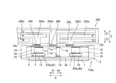
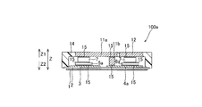
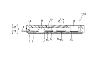
- FIG. 5 is a sectional view taken along line 400-400 in FIG.
- FIG. 5 is a cross-sectional view taken along line 500-500 in FIG.
- FIG. 5 is a sectional view taken along line 400-400 in FIG.
- FIG. 5 is a cross-sectional view taken along line 600-600 in FIG.
- FIG. 7 is a cross-sectional view taken along line 700-700 in FIG. It is a disassembled perspective view for demonstrating the internal structure of the power module main-body part by 1st Embodiment of this invention.
- 1 is a circuit diagram of a power module according to a first embodiment of the present invention.
- 1 is a circuit diagram of a chopper circuit to which a power module according to a first embodiment of the present invention is applied.
- It is a circuit diagram of a chopper circuit to which a power module according to a comparative example is applied.
- It is a figure which shows the result of the simulation of the chopper circuit to which the power module by a comparative example was applied.
- the power module 100 is an example of the “power converter” in the present invention.
- the power module 100 includes three power module main body portions 100 a, 100 b and 100 c and a wiring board 200.
- the power module main body portions 100a, 100b, and 100c are examples of the “power conversion device main body portion” in the present invention.
- the power module 100 constitutes a three-phase inverter circuit connected to a motor or the like.
- the portions on the arrow X1 direction side of the power module main body portions 100a, 100b and 100c constituting the power module 100 function as the upper arm (P side) of the three-phase inverter circuit.
- the portions on the arrow X2 direction side of the power module main body portions 100a, 100b, and 100c function as the lower arm (N side) of the three-phase inverter circuit.
- the power module main-body parts 100a, 100b, and 100c shall perform the power conversion of U phase, V phase, and W phase, respectively.
- the power module main body portions 100a, 100b, and 100c have substantially the same configuration, the power module main body portion 100a will be mainly described below.
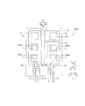
- a P-phase bus bar 200a, a U-phase bus bar 200b, and an N-phase bus bar 200c made of a conductive metal plate are provided inside the wiring board 200. Further, as shown in FIG. 1, some of these P-phase bus bars 200a, U-phase bus bars 200b, and N-phase bus bars 200c are a P-side terminal connection portion 10a and a U-phase terminal connection portion, which will be described later, of the power module main body 100a. It is exposed from the lower surface (surface on the arrow Z2 direction side) of the wiring board 200 so as to correspond to 11c and the N-side terminal connecting portion 12b. Note that a V-phase bus bar and a W-layer bus bar are provided inside the wiring board 200 so as to correspond to a V-phase terminal connection portion and a W-phase terminal connection portion described later of the power module main body portions 100b and 100c.
- the power module main body 100a is configured to be electrically connected to the wiring board 200 on the upper surface (surface on the arrow Z1 direction side) of the power module main body 100a. Specifically, as shown in FIGS. 1 to 3, a P-side terminal connecting portion 10a, a U-phase terminal connecting portion 11c, and an N-side terminal connecting portion 12b (to be described later in detail) of the power module main body 100a Part) and a portion of the P-phase bus bar 200a, the U-phase bus bar 200b, and the N-phase bus bar 200c of the wiring board 200 that are exposed from the lower surface (the surface on the arrow Z2 direction side) of the wiring board 200 are joined via the bump electrode 300. It is configured to be.
- the power module main body 100a and the wiring board 200 are configured to be arranged with a predetermined distance (space) therebetween.
- This space is filled with, for example, a resin having thermal conductivity.
- the resin can suppress corrosion of the P-phase bus bar 200a, the N-phase bus bar 200c, and the U-phase bus bar 200b that connect the power module main body 100a and the wiring board 200.
- a thermally conductive compound may be used instead of the resin.
- the power module main body 100a includes a metal plate 1, an insulating substrate 2, a P-side conductive plate 3, a first N-side conductive plate 4a, and a second N-side conductive plate 4b.
- a U-phase terminal 11, an N-side terminal 12, and a snubber capacitor 13 are provided.
- the metal plate 1 is an example of the “back side electrode” in the present invention.
- the P-side conductive plate 3 is an example of the “first conductive plate” in the present invention.
- the first N-side conductive plate 4a is an example of the “second conductive plate” and the “element-side second conductive plate” in the present invention.
- the second N-side conductive plate 4b is an example of the “second conductive plate” and the “terminal-side second conductive plate” in the present invention.
- the columnar electrode 7 is an example of the “electrode conductor” in the present invention.
- the N-side terminal 12 is an example of the “negative input / output terminal” in the present invention.
- the snubber capacitor 13 is an example of the “capacitor” in the present invention.
- the snubber capacitor 13 is covered with a case 14 made of resin or the like. Further, the P-side terminal 10, the U-phase terminal 11, and the N-side terminal 12 are exposed from the upper surface (surface on the arrow Z1 direction side) of the case 14.
- the metal plate 1, the P-side conductive plate 3, the first N-side conductive plate 4a, and the second N-side conductive plate 4b are made of a metal such as copper.
- the insulating substrate 2 is made of an insulating material such as ceramic.
- the metal plate 1, the insulating substrate 2 and the P-side conductive plate 3 constitute a P-side insulating circuit substrate, and the metal plate 1, the insulating substrate 2, the first N-side conductive plate 4a and the second N-side plate.
- the N-side insulated circuit board is configured by the side conductive plate 4b.
- the P-side semiconductor element 5 is an example of the “first power conversion semiconductor element” in the present invention.
- the N-side semiconductor element 6 is an example of the “second power conversion semiconductor element” in the present invention.
- the two P-side semiconductor elements 5 are composed of one P-side transistor element 5a and one P-side diode element 5b.
- the P-side transistor element 5a is, for example, a MOSFET (field effect transistor).
- the P-side diode element 5b is, for example, an SBD (Schottky barrier diode).
- the P-side diode element 5b functions as a free wheel diode. As shown in FIG. 11, the P-side transistor element 5a and the P-side diode element 5b are electrically connected in parallel. Specifically, the cathode electrode of the P-side diode element 5b is electrically connected to the drain electrode of the P-side transistor element 5a.
- the anode electrode of the P-side diode element 5b is electrically connected to the source electrode of the P-side transistor element 5a.
- the P-side transistor element 5a is an example of the “voltage-driven transistor element” in the present invention.
- the P-side diode element 5b is an example of the “freewheeling diode element” in the present invention.
- the drain electrode of the P-side transistor element 5 a and the cathode electrode of the P-side diode element 5 b are electrically connected to the P-side conductive plate 3.
- the lower surface (surface on the arrow Z2 direction side) of the P-side transistor element 5a and the P-side diode element 5b is connected to the upper surface (arrow Z1 direction) of the P-side conductive plate 3 with a bonding material 15 made of solder. Side surface).
- the P-side transistor element 5a and the P-side diode element 5b are arranged side by side at a predetermined interval in the Y direction on the surface of the P-side conductive plate 3.
- the P-side transistor element 5a is disposed on the arrow Y1 direction side of the P-side diode element 5b.
- a bonding material made of Ag nanopaste may be used.
- the two N-side semiconductor elements 6 are composed of one N-side transistor element 6a and one N-side diode element 6b.
- the N-side diode element 6b functions as a free wheel diode.
- the N-side transistor element 6a and the N-side diode element 6b are electrically connected in parallel.
- the cathode electrode of the N-side diode element 6b is electrically connected to the drain electrode of the N-side transistor element 6a.
- the anode electrode of the N-side diode element 6b is electrically connected to the source electrode of the N-side transistor element 6a.
- the N-side transistor element 6a is an example of the “voltage-driven transistor element” in the present invention.
- the N-side diode element 6b is an example of the “freewheeling diode element” in the present invention.
- the N-side transistor element 6a and the N-side diode element 6b are arranged side by side in the Y direction on the upper surface (the surface on the arrow Z1 direction side) of the first N-side conductive plate 4a.
- the N-side transistor element 6a is arranged on the arrow Y1 direction side with respect to the N-side diode element 6b.
- the P-side transistor element 5a and the N-side transistor element 6a, and the P-side diode element 5b and the N-side diode element 6b are arranged side by side in the X direction.
- the P-side transistor element 5a and the P-side diode element 5b are arranged on the arrow X1 direction side with respect to the N-side transistor element 6a and the N-side diode element 6b.
- the two P-side control terminals 8 are respectively connected to the gate electrode and the source electrode provided on the upper surface (the surface on the arrow Z1 direction side) of the P-side transistor element 5a through wire 8a by wire bonding.
- the two N-side control terminals 9 are respectively connected to the gate electrode and the source electrode provided on the upper surface of the N-side transistor element 6a through wire 9a by wire bonding.
- the two P-side control terminals 8 and the two N-side control terminals 9 protrude from the side surface of the case 14 of the power module main body 100a on the arrow Y1 direction side to the arrow Y1 direction side.
- the P-side terminal 10 is configured to be bonded to the upper surface (surface on the arrow Z1 direction side) of the P-side conductive plate 3 through the bonding material 15.
- the P-side terminal 10 is configured to be electrically connected to the drain electrode of the P-side transistor element 5a and the cathode electrode of the P-side diode element 5b through the P-side conductive plate 3.
- the P-side terminal 10 is formed in a column shape extending in the Z direction.
- the U-phase terminal 11 includes a U-phase terminal portion 11a and a P-side / N-side connection electrode portion 11b. As shown in FIG. 10, the U-phase terminal portion 11a is formed in a flat plate shape that extends in the X direction and the Y direction. Further, the P-side / N-side connection electrode portion 11b is formed in a column shape extending in the Y direction and the Z direction.
- the U-phase terminal portion 11a is bonded to the upper surfaces of the two columnar electrodes 7 bonded to the upper surfaces (the surfaces on the arrow Z1 direction side) of the P-side transistor element 5a and the P-side diode element 5b via the bonding material 15. It is comprised so that.
- the U-phase terminal portion 11a is configured to be electrically connected to the source electrode of the P-side transistor element 5a and the anode electrode of the P-side diode element 5b via the two columnar electrodes 7. .
- the columnar electrode 7 is formed in a columnar shape extending in the Z direction in which the upper end surface is formed substantially flat.
- the P-side / N-side connection electrode portion 11b is configured to be bonded to the upper surface (surface on the arrow Z1 direction side) of the first N-side conductive plate 4a via the bonding material 15.
- the P-side-N-side connection electrode portion 11b is connected to the P-side semiconductor element 5 (P-side transistor element 5a and P-side diode element 5b) connected to the U-phase terminal portion 11a and the first N-side conductive plate 4a.
- N-side semiconductor element 6 N-side transistor element 6a and N-side diode element 6b to be electrically connected.
- the source electrode of the P-side transistor element 5a and the anode electrode of the P-side diode element 5b, and the drain electrode of the N-side transistor element 6a and the cathode electrode of the N-side diode element 6b are for P-side / N-side connection. It is electrically connected by the electrode part 11b.
- the N-side terminal 12 is formed in a flat plate shape extending in the X direction and the Y direction, and is joined to the upper surface (surface on the arrow Z1 direction side) of the second N-side conductive plate 4b via the connection electrode 12a. Further, the N-side terminal 12 is bonded to the upper surfaces of the two columnar electrodes 7 bonded to the upper surfaces (surfaces on the arrow Z1 direction side) of the N-side transistor element 6a and the N-side diode element 6b through the bonding material 15, respectively. It is configured to be.
- the N-side terminal 12 is configured to be electrically connected to the source electrode of the N-side transistor element 6a and the anode electrode of the N-side diode element 6b via the two columnar electrodes 7.
- the P-side terminal connection portion 10a, the U-phase terminal connection portion 11c, and the N-side terminal connection portion are provided on the upper surfaces (surfaces on the arrow Z1 direction side) of the P-side terminal 10, U-phase terminal 11, and N-side terminal 12, respectively. 12b (refer to the fine dot-shaped shaded portions in FIGS. 1, 4 and 10).
- These P-side terminal connection portion 10 a, U-phase terminal connection portion 11 c, and N-side terminal connection portion 12 b are provided for electrical connection with the wiring board 200.
- the P-side terminal connection portion 10a, the U-phase terminal connection portion 11c, and the N-side terminal connection portion 12b are an inflow port and an outflow port for current flowing in and out between the power module main body 100a and the wiring board 200.
- the power module main body 100b includes a P-side terminal connection portion, a V-phase terminal connection portion, and an N-phase so as to correspond to the P-side terminal connection portion 10a, U-phase terminal connection portion 11c, and N-side terminal connection portion 12b.
- a side terminal connection portion is provided, and a P-side terminal connection portion, a W-phase terminal connection portion, and an N-side terminal connection portion are provided in the power module main body portion 100c.
- the snubber capacitor 13 is provided so as to be directly connected to the P-side conductive plate 3 and the second N-side conductive plate 4b.
- the snubber capacitor 13 is disposed so as to straddle the P-side conductive plate 3 and the second N-side conductive plate 4b.
- the snubber capacitor 13 is provided with electrodes 13a at the end in the arrow X1 direction and the end in the arrow X2 direction, respectively.
- a portion 13b between the electrodes 13a of the snubber capacitor 13 is made of ceramic.
- the electrode 13a, the P-side conductive plate 3, and the second N-side conductive plate 4b are joined by solder 13c.
- the snubber capacitor 13 is electrically connected to the drain electrode of the P-side transistor element 5a and the source electrode of the N-side transistor element 6a.
- the snubber capacitor 13 is electrically connected to the cathode electrode of the P-side diode element 5b and the anode electrode of the N-side diode element 6b.
- the snubber capacitor 13 has a function of suppressing a surge voltage generated when the P-side transistor element 5a and the N-side transistor element 6a are switched. Note that a bonding material made of Ag nanopaste may be used instead of the solder 13c.
- the snubber capacitor 13 is disposed in a region surrounded by the columnar electrodes 7 when viewed in plan (viewed from above). Further, the snubber capacitor 13 is directly connected to the P-side conductive plate 3 and the second N-side conductive plate 4b on the side opposite to the wiring board 200 (see FIG. 1) inside the power module main body 100a without wiring. Is arranged.
- a chopper in which a DC power source 21, an electrolytic capacitor 22, a gate circuit 23, and a load reactor 24 are connected to the power module main body 100a (dotted line) according to the first embodiment.
- a circuit 25 was assumed.
- the DC power source 21 is connected to the P-side terminal 10 and the N-side terminal 12 of the power module main body 100a.
- the electrolytic capacitor 22 is connected between the DC power supply 21 and the P-side terminal 10 and between the DC power supply 21 and the N-side terminal 12.
- the gate circuit 23 is connected to the N-side control terminal 9.
- the source current Is flowing through the N-side terminal 12 of the power module main body 100a was obtained by simulation. Further, the voltage Vds between the N-side terminal 12 of the power module main body 100a and the U-phase terminal 11 was obtained by simulation.
- a chopper circuit 801 in which a DC power source 21, an electrolytic capacitor 22, and a gate circuit 23 are connected to two power module main body portions 800a and 800b (dotted lines) is assumed.
- the power module main body 800a (800b) according to the comparative example is provided with one P-side transistor element 802 (N-side transistor element 804) and one P-side diode element 803 (N-side diode element 805).
- the chopper circuit 801 is provided with a snubber capacitor 808 between the P-side terminal 806 of the power module main body 800a and the N-side terminal 807 of the power module main body 800b.
- the source current Is flowing through the N-side terminal 807 of the power module main body 800b was obtained by simulation. Further, the voltage Vds between the N-side terminal 807 and the U-phase terminal 809 of the power module main body 800b was obtained by simulation.
- the voltage of the DC power source 21 is assumed to be 300 V, and the source current Is when the power module main body is in the on state is assumed to be 200 A.
- the carrier frequency (the frequency of the modulation wave for determining the pulse width of the output voltage by the inverter during PWM control) was assumed to be 100 kHz.
- the wiring inductance inside the power module main body portions 800a and 800b according to the comparative example is assumed to be 7.426 nH
- the wiring inductance inside the power module main body portion 100a according to the first embodiment is assumed to be 3.0898 nH.
- the P-side transistor element 5a, the P-side diode element 5b, the N-side transistor element 6a, and the N-side diode element 6b are included in one power module main body 100a.
- the P-side transistor element 802 and the P-side diode element 803, and the N-side transistor element 804 and the N-side diode element 805 are provided in separate power module main body portions. It has been. For this reason, the wiring inductance inside the power module main body portions 800a and 800b according to the comparative example is made larger than the wiring inductance inside the power module main body portion 100a according to the first embodiment.
- FIG. 14 shows the result of the simulation according to the comparative example.
- the vertical axis represents voltage (V) and source current Is (A), and the horizontal axis represents time.
- FIG. 15 shows the result of the simulation according to the first embodiment.
- the energy accumulated in the wiring inductance resonates in the closed circuit (one-dot chain line, LC circuit) shown in FIG.
- surge voltage was generated and ringing was generated.
- the P-side semiconductor element 5 disposed on the surface of the P-side conductive plate 3 and the surface of the second N-side conductive plate 4b are disposed, and By providing the N-side semiconductor element 6 to be connected to the power module main body 100a, the P-side semiconductor element 5 and the N-side semiconductor element 6 are separately provided on two different power module main bodies, respectively. Compared to the case, the distance between the P-side semiconductor element 5 and the N-side semiconductor element 6 can be reduced, so that the wiring inductance between the P-side semiconductor element 5 and the N-side semiconductor element 6 can be reduced. Can do.
- a snubber capacitor 13 is provided between the P-side semiconductor element 5 and the N-side semiconductor element 6 so as to be connected to the P-side conductive plate 3 and the second N-side conductive plate 4b in the power module main body 100a.
- the destruction of the P-side semiconductor element 5 and the N-side semiconductor element 6 due to the surge voltage can be suppressed, and compared to the case where the snubber capacitor 13 is provided on the substrate outside the power module main body 100a, Since the distance between the P-side semiconductor element 5 and the N-side semiconductor element 6 and the snubber capacitor 13 is reduced, the wiring inductance between the P-side semiconductor element 5 and the N-side semiconductor element 6 and the snubber capacitor 13 is reduced. Can do.
- the snubber capacitor 13 is directly connected to the P-side conductive plate 3 and the second N-side conductive plate 4 b between the P-side semiconductor element 5 and the N-side semiconductor element 6.
- condenser 13 the P side conductive plate 3, and the 2nd N side conductive plate 4b can be made small.
- the snubber capacitor 13 extends between the P-side conductive plate 3 and the second N-side conductive plate 4 b between the P-side semiconductor element 5 and the N-side semiconductor element 6. Deploy.
- the snubber capacitor 13 and the P-side conductive plate 3 can be easily connected directly, and the snubber capacitor 13 and the second N-side conductive plate 4b can be easily connected directly.
- the source electrode of the P-side semiconductor element 5 and the drain electrode of the N-side semiconductor element 6 are electrically connected to each other, and the snubber capacitor 13 is connected to the P-side conductive plate 3. Is electrically connected to the drain electrode of the P-side semiconductor element 5 via the second N-side conductive plate 4b and electrically connected to the source electrode of the N-side semiconductor element 6 via the second N-side conductive plate 4b. Thereby, the surge voltage generated when the P-side semiconductor element 5 and the N-side semiconductor element 6 are switched can be suppressed by the snubber capacitor 13.
- the power module main body 100a is formed on the surface of the P-side semiconductor element 5 formed on the surface of the P-side conductive plate 3 and the surface of the first N-side conductive plate 4a.
- the snubber capacitor 13 is seen in a plan view, including a columnar electrode 7 formed on the surface of the N-side semiconductor element 6 and having a columnar shape extending upward and having a columnar upper end surface formed substantially flat. And disposed in a region surrounded by the columnar electrode 7. Thereby, unlike the case where the snubber capacitor 13 is disposed outside the region surrounded by the columnar electrodes 7, it is possible to suppress the power module main body 100a from becoming large.
- the columnar electrode 7 has a columnar shape extending upward, and the columnar upper end surface is formed to be substantially flat, so that the wiring inductance can be reduced unlike the case where the electrode is a thin wire shape, for example. As a result, it is possible to prevent the P-side semiconductor element 5 and the N-side semiconductor element 6 from operating at high speed due to the large wiring inductance. Moreover, since the amount of heat radiation can be increased by the columnar columnar electrode 7 as compared with the case of using a thin wire-shaped electrode, the heat dissipation can be improved.
- the power module main body 100a has the P-side conductive plate 3, the first N-side conductive plate 4a, and the second N-side conductive plate 4b formed on the front surface, and the metal plate 1 on the back surface.
- the snubber capacitor 13 is disposed so as to directly connect the P-side conductive plate 3 and the second N-side conductive plate 4b.
- the P-side conductive plate 3, the first N-side conductive plate 4a, the second N-side conductive plate 4b, and the snubber capacitor 13 are formed on the surface of one insulating substrate 2, so that the P-side conductive plate 3, the first N Unlike the case where the side conductive plate 4a, the second N-side conductive plate 4b, and the snubber capacitor 13 are formed on different insulating substrates, the power module main body 100a can be prevented from becoming large.
- the snubber capacitor 13 is directly connected to the P-side conductive plate 3 and the second N-side conductive plate 4b on the side opposite to the wiring board 200 inside the power module main body 100a.
- the snubber capacitor 13 is disposed on the P-side conductive plate 3 and the second N-side conductive plate 4b side, so that the distance between the snubber capacitor 13 and the P-side conductive plate 3 and the second N-side conductive plate 4b is reduced. Get smaller.
- the wiring inductance between the snubber capacitor 13 and the P-side conductive plate 3 and the second N-side conductive plate 4b can be reduced.
- the power module main body 101 of the second embodiment will be described with reference to FIGS.
- the P-side semiconductor is sandwiched between two insulating substrates. An element and an N-side semiconductor element are provided.
- the insulating substrate 112a and the insulating substrate 112b are arranged to face each other.
- the insulating substrate 112a includes a metal plate 111a, an insulating substrate 112a, a P-side conductive plate 113, a first N-side conductive plate 114a, two P-side semiconductor elements 115, two columnar electrodes 117, and two P-type electrodes.
- a side control terminal 118, a P side terminal 120, an N side terminal 122, and a snubber capacitor 123 are provided.
- the metal plate 111a is grounded.
- the metal plate 111a is an example of the “back side electrode” in the present invention.
- the insulating substrate 112a and the insulating substrate 112b are examples of the “first insulating substrate” and the “second insulating substrate” in the present invention, respectively.
- the P-side conductive plate 113 is an example of the “first conductive plate” in the present invention.
- the first N-side conductive plate 114a is an example of the “second conductive plate” in the present invention.
- the columnar electrode 117 is an example of the “electrode conductor” in the present invention.
- the N-side terminal 122 is an example of the “negative input / output terminal” in the present invention.
- the snubber capacitor 123 is an example of the “capacitor” in the present invention.
- the insulating substrate 112b of the power module main body 101 includes a metal plate 111b, a second N-side conductive plate 114b, two N-side semiconductor elements 116, and two columnar electrodes. 117, two N-side control terminals 119, and a U-phase terminal 121 are provided. Further, unlike the metal plate 111a, the metal plate 111b is not grounded (see FIGS. 18 and 19). Thereby, unlike the case where both metal plate 111a and metal plate 111b are grounded, the stray capacitance between U-phase terminal 121 and ground (earth) is reduced. As a result, common mode noise can be reduced.
- the metal plate 111a, the P-side conductive plate 113, the first N-side conductive plate 114a, the metal plate 111b, and the second N-side conductive plate 114b are made of a metal such as copper.
- the insulating substrates 112a and 112b are made of an insulator such as ceramic.
- the metal plate 111a, the insulating substrate 112a, and the P-side conductive plate 113 constitute a P-side insulating circuit substrate, and the metal plate 111a, the insulating substrate 112a, and the first N-side conductive plate 114a An insulated circuit board on the side is configured.
- the metal plate 111b, the insulating substrate 112b, and the second N-side conductive plate 114b constitute an N-side insulating circuit substrate.
- the P-side semiconductor element 115 is an example of the “first power conversion semiconductor element” in the present invention.
- the N-side semiconductor element 116 is an example of the “second power conversion semiconductor element” in the present invention.
- the two P-side semiconductor elements 115 are composed of one P-side transistor element 115a and one P-side diode element 115b.
- the P-side transistor element 115a is, for example, a MOSFET (field effect transistor).
- the P-side diode element 115b is, for example, an SBD (Schottky barrier diode).
- the P-side diode element 115b has a function as a free wheel diode.
- the P-side transistor element 115a and the P-side diode element 115b are electrically connected in parallel.
- the cathode electrode of the P-side diode element 115b is electrically connected to the drain electrode of the P-side transistor element 115a.
- the anode electrode of the P-side diode element 115b is electrically connected to the source electrode of the P-side transistor element 115a.
- the P-side transistor element 115a is an example of the “voltage-driven transistor element” in the present invention.
- the P-side diode element 115b is an example of the “freewheeling diode element” in the present invention.
- the drain electrode of the P-side transistor element 115 a and the cathode electrode of the P-side diode element 115 b are electrically connected to the P-side conductive plate 113.
- the lower surfaces (the surfaces on the arrow Z2 direction side) of the P-side transistor element 115a and the P-side diode element 115b are connected to the upper surface (the arrow Z1 direction) of the P-side conductive plate 113 through a bonding material 125 made of solder. Side surface).
- the P-side transistor element 115a and the P-side diode element 115b are arranged side by side with a predetermined interval in the Y direction on the surface of the P-side conductive plate 113.
- the P-side transistor element 115a is disposed on the arrow Y2 direction side of the P-side diode element 115b.
- a bonding material made of Ag nanopaste may be used.
- the two N-side semiconductor elements 116 are composed of one N-side transistor element 116a and one N-side diode element 116b.
- the N-side diode element 116b functions as a free wheel diode.
- the N-side transistor element 116a and the N-side diode element 116b are electrically connected in parallel.
- the cathode electrode of the N-side diode element 116b is electrically connected to the drain electrode of the N-side transistor element 116a.
- the anode electrode of the N-side diode element 116b is electrically connected to the source electrode of the N-side transistor element 116a.
- the N-side transistor element 116a is an example of the “voltage-driven transistor element” in the present invention.
- the N-side diode element 116b is an example of the “freewheeling diode element” in the present invention.
- the N-side transistor element 116a and the N-side diode element 116b are arranged side by side in the Y direction on the upper surface (the surface on the arrow Z2 direction side) of the second N-side conductive plate 114b.
- the N-side transistor element 116a is disposed on the arrow Y2 direction side with respect to the N-side diode element 116b.
- the P-side transistor element 115a and the N-side transistor element 116a, and the P-side diode element 115b and the N-side diode element 116b are respectively They are arranged side by side in the X direction.
- the P-side transistor element 115a and the P-side diode element 115b are arranged on the arrow X1 direction side of the N-side transistor element 116a and the N-side diode element 116b.
- the two P-side control terminals 118 are respectively connected to the gate electrode and the source electrode provided on the upper surface (surface on the arrow Z1 direction side) of the P-side transistor element 115a by wire bonding. Connected through.
- the two N-side control terminals 119 are respectively connected to the gate electrode and the source electrode provided on the upper surface of the N-side transistor element 116a through wire 119a by wire bonding. ing.
- the P-side terminal 120 is configured to be joined to the upper surface (the surface on the arrow Z1 direction side) of the P-side conductive plate 113.
- the P-side terminal 120 is configured to be electrically connected to the drain electrode of the P-side transistor element 115a and the cathode electrode of the P-side diode element 115b via the P-side conductive plate 113.
- the P-side terminal 120 is formed in a flat plate shape extending in the X direction and the Y direction.
- the N-side terminal 122 is configured to be joined to the upper surface (the surface on the arrow Z1 direction side) of the first N-side conductive plate 114a.
- the N-side terminal 122 is arranged so that the insulating substrate 112a and the insulating substrate 112b face each other, the source electrode of the N-side transistor element 116a and the N-side diode element 116b through the first N-side conductive plate 114a. It is configured to be electrically connected to the anode electrode.
- the N-side terminal 122 is formed in a flat plate shape extending in the X direction and the Y direction.
- the U-phase terminal 121 is configured to be joined to the upper surface (the surface on the arrow Z2 direction side) of the second N-side conductive plate 114b.
- the U-phase terminal 121 is configured to be electrically connected to the drain electrode of the N-side transistor element 116a and the cathode electrode of the N-side diode element 116b via the second N-side conductive plate 114b.
- U-phase terminal 121 is formed in a flat plate shape extending in the X direction and the Y direction.
- the P-side terminal 120, the N-side terminal 122, and the U-phase terminal 121 are provided for electrical connection with a wiring board (not shown).
- the P-side terminal 120, the N-side terminal 122, and the U-phase terminal 121 function as an inflow port and an outflow port for current flowing in and out between the power module main body 101 and the wiring board.
- the snubber capacitor 123 is directly connected to the P-side conductive plate 113 and the first N-side conductive plate 114 a provided on the insulating substrate 112 a side without using a wiring. Is arranged. Further, the snubber capacitor 123 is disposed so as to straddle the P-side conductive plate 113 and the first N-side conductive plate 114a. An electrode 123a is provided at each end of the snubber capacitor 123 in the arrow X1 direction and at the end in the arrow X2 direction. Further, the portion 123b between the electrodes 123a of the snubber capacitor 123 is made of ceramic.
- the electrode 123a, the P-side conductive plate 113, and the first N-side conductive plate 114a are joined by solder 123c.
- the snubber capacitor 123 is electrically connected to the drain electrode of the P-side transistor element 115a and the source electrode of the N-side transistor element 116a. Is done.
- the snubber capacitor 123 is electrically connected to the cathode electrode of the P-side diode element 115b and the anode electrode of the N-side diode element 116b.
- the power module main body 101 performs U-phase power conversion.
- the power module main body that performs V-phase and W-phase power conversion also has substantially the same configuration as the power module main body 101.
- the power module main body 101 includes the insulating substrate 112a in which the P-side conductive plate 113 and the first N-side conductive plate 114a are formed on the front surface, and the metal plate 111a is formed on the back surface.
- An insulating substrate 112b disposed so as to face the insulating substrate 112a with the P-side semiconductor element 115 and the N-side semiconductor element 116 interposed between the insulating substrate 112b and the snubber capacitor 123 on the insulating substrate 112a side.
- the P-side conductive plate 113 and the first N-side conductive plate 114a are directly connected.
- the snubber capacitor 123 is disposed on the P-side conductive plate 113 and the first N-side conductive plate 114a side, so that the distance between the snubber capacitor 123 and the P-side conductive plate 113 and the first N-side conductive plate 114a is reduced. Get smaller. Thereby, the wiring inductance between the snubber capacitor 123 and the P-side conductive plate 113 and the first N-side conductive plate 114a can be reduced.
- MOSFET field effect transistor
- SBD Schottky barrier diode
- MOSFET insulated gate bipolar transistor
- IGBT insulated gate bipolar transistor
- the present invention is not limited to this.
- other diodes such as FRD (fast recovery diode) may be used as long as they are free-wheeling diodes.
- the present invention is not limited to this.
- a plurality of sets of MOSFETs and SBDs may be arranged on each of the P side and the N side of the power module main body.
- the example in which the snubber capacitor is arranged so as to be directly connected to the P-side conductive plate and the first N-side conductive plate by soldering without wiring is shown. Not limited to this.
- the snubber capacitor only needs to be provided inside the power module main body.
- the snubber capacitor may be connected to the P-side conductive plate and the first N-side conductive plate between the P-side conductive plate and the first N-side conductive plate via a short wiring.
Landscapes
- Engineering & Computer Science (AREA)
- Power Engineering (AREA)
- Inverter Devices (AREA)
- Power Conversion In General (AREA)
Abstract
サージ電圧に起因する電力変換用半導体素子の破壊を抑制しながら、装置全体の配線インダクタンスを小さくすることが可能な電力変換装置を提供する。 このパワーモジュール100は、パワーモジュール本体部100aを備え、パワーモジュール本体部100aは、パワーモジュール本体部100a内に間隔を隔てて配置されたP側導電板3、第1N側導電板4aおよび第2N側導電板4bと、P側導電板3の表面上に配置されるP側半導体素子5と、第1N側導電板4aの表面上に配置され、P側半導体素子5と電気的に接続されるN側半導体素子6と、パワーモジュール本体部100aの内部において、P側半導体素子5とN側半導体素子6との間にP側導電板3と第2N側導電板4bとに接続するように配置され、サージ電圧を抑制するためのコンデンサ13とを含む。
Description
本発明は、電力変換装置に関し、特に、電力変換用半導体素子を備える電力変換装置に関する。
従来、電力変換用半導体素子を備える電力変換装置が知られている(たとえば、特許文献1参照)。
上記特許文献1には、IGBT(電力変換用半導体素子)と、IGBTに電気的に接続されるリードフレームと、IGBTとリードフレームとを内部に含むように設けられるモールド樹脂とを備える半導体装置(電力変換装置)が開示されている。この半導体装置では、IGBTがスイッチングされることにより、IGBTのコレクタとエミッタとの間で、電流が流れるように構成されている。
しかしながら、上記特許文献1に記載の半導体装置では、IGBT(電力変換用半導体素子)がスイッチングされる際に、サージ電圧が発生することにより、電力変換用半導体素子が破壊される場合があるという問題点がある。また、一般に、上記のような従来の電力変換装置では、装置全体の配線インダクタンスを小さくすることが望まれている。
この発明は、上記のような課題を解決するためになされたものであり、この発明の1つの目的は、サージ電圧に起因する電力変換用半導体素子の破壊を抑制しながら、装置全体の配線インダクタンスを小さくすることが可能な電力変換装置を提供することである。
上記目的を達成するために、この発明の一の局面による電力変換装置は、電力変換装置本体部を備え、電力変換装置本体部は、電力変換装置本体部内に間隔を隔てて配置された第1導電板および第2導電板と、第1導電板の表面上に配置される第1電力変換用半導体素子と、第2導電板の表面上に配置され、第1電力変換用半導体素子と電気的に接続される第2電力変換用半導体素子と、電力変換装置本体部の内部において、第1電力変換用半導体素子と第2電力変換用半導体素子との間に第1導電板と第2導電板とに接続するように配置され、サージ電圧を抑制するためのコンデンサとを含む。
この一の局面による電力変換装置では、上記のように、第1導電板の表面上に配置される第1電力変換用半導体素子と、第2導電板の表面上に配置され、第1電力変換用半導体素子と電気的に接続される第2電力変換用半導体素子とを電力変換装置本体部に設けることによって、第1電力変換用半導体素子と第2電力変換用半導体素子とが、それぞれ、異なる2つの電力変換装置本体部に別個に設けられる場合と比べて、第1電力変換用半導体素子と第2電力変換用半導体素子との間の距離を小さくすることができるので、第1電力変換用半導体素子と第2電力変換用半導体素子との間の配線インダクタンスを小さくすることができる。また、電力変換装置本体部の内部において、第1電力変換用半導体素子と第2電力変換用半導体素子との間に第1導電板と第2導電板とに接続するようにコンデンサを設けることによって、サージ電圧に起因する電力変換用半導体素子の破壊を抑制することができるとともに、コンデンサが電力変換装置本体部の外部に設けられる場合と比べて、第1電力変換用半導体素子および第2電力変換用半導体素子とコンデンサとの間の距離が小さくなるので、第1電力変換用半導体素子および第2電力変換用半導体素子とコンデンサとの間の配線インダクタンスを小さくすることができる。
以下、本発明の実施形態を図面に基づいて説明する。
(第1実施形態)
まず、図1~図3を参照して、本発明の第1実施形態によるパワーモジュール100の構成について説明する。なお、パワーモジュール100は、本発明の「電力変換装置」の一例である。
まず、図1~図3を参照して、本発明の第1実施形態によるパワーモジュール100の構成について説明する。なお、パワーモジュール100は、本発明の「電力変換装置」の一例である。
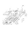
図1に示すように、本発明の第1実施形態によるパワーモジュール100は、3つのパワーモジュール本体部100a、100bおよび100cと、配線基板200とにより構成されている。なお、パワーモジュール本体部100a、100bおよび100cは、それぞれ、本発明の「電力変換装置本体部」の一例である。
パワーモジュール100は、モータなどに接続される3相インバータ回路を構成している。このパワーモジュール100を構成するパワーモジュール本体部100a、100bおよび100cのそれぞれの矢印X1方向側の部分は、3相インバータ回路の上側アーム(P側)として機能する。また、パワーモジュール本体部100a、100bおよび100cのそれぞれの矢印X2方向側の部分は、3相インバータ回路の下側アーム(N側)として機能する。なお、パワーモジュール本体部100a、100bおよび100cは、それぞれ、U相、V相、W相の電力変換を行うものとする。また、パワーモジュール本体部100a、100bおよび100cは、それぞれ、略同様の構成を有しているので、以下では、主としてパワーモジュール本体部100aについて説明する。
図2に示すように、配線基板200の内部には、導電性の金属板からなるP相ブスバ200a、U相ブスバ200bおよびN相ブスバ200cが設けられている。また、図1に示すように、これらのP相ブスバ200a、U相ブスバ200bおよびN相ブスバ200cの一部は、パワーモジュール本体部100aの後述するP側端子接続部10a、U相端子接続部11cおよびN側端子接続部12bに対応するように配線基板200の下面(矢印Z2方向側の面)から露出している。なお、配線基板200の内部には、パワーモジュール本体部100bおよび100cの後述するV相端子接続部およびW相端子接続部に対応するように、V相ブスバおよびW層ブスバが設けられている。
パワーモジュール本体部100aは、パワーモジュール本体部100aの上面(矢印Z1方向側の面)において配線基板200に電気的に接続されるように構成されている。具体的には、図1~図3に示すように、パワーモジュール本体部100aの後述するP側端子接続部10a、U相端子接続部11cおよびN側端子接続部12b(細かい点状の網掛け部参照)と、配線基板200のP相ブスバ200a、U相ブスバ200bおよびN相ブスバ200cの配線基板200の下面(矢印Z2方向側の面)から露出した部分とがバンプ電極300を介して接合されるように構成されている。
また、図3に示すように、パワーモジュール本体部100aと配線基板200とは、所定の距離(空間)を隔てて配置されるように構成されている。この空間には、たとえば、熱伝導性を有する樹脂などが充填される。これにより、パワーモジュール100の放熱性を高めながら、パワーモジュール本体部100a、パワーモジュール本体部100bおよびパワーモジュール本体部100cと、配線基板200とを固定することが可能になる。また、樹脂により、パワーモジュール本体部100aと配線基板200とを接続するP相ブスバ200a、N相ブスバ200c、U相ブスバ200bが腐食するのを抑制することが可能になる。なお、樹脂の代わりに、熱伝導性のコンパウンドを用いてもよい。
次に、図4~図11を参照して、本発明の第1実施形態によるパワーモジュール本体部100aの詳細な構成について説明する。
図4~図10に示すように、パワーモジュール本体部100aには、金属板1と、絶縁基板2と、P側導電板3と、第1N側導電板4aと、第2N側導電板4bと、2つのP側半導体素子5と、2つのN側半導体素子6と、4つの柱状電極7と、2つのP側制御端子8と、2つのN側制御端子9と、P側端子10と、U相端子11と、N側端子12と、スナバコンデンサ13とが設けられている。なお、金属板1は、本発明の「裏面側電極」の一例である。また、P側導電板3は、本発明の「第1導電板」の一例である。また、第1N側導電板4aは、本発明の「第2導電板」および「素子側第2導電板」の一例である。また、第2N側導電板4bは、本発明の「第2導電板」および「端子側第2導電板」の一例である。また、柱状電極7は、本発明の「電極用導体」の一例である。また、N側端子12は、本発明の「負側入出力端子」の一例である。また、スナバコンデンサ13は、本発明の「コンデンサ」の一例である。
また、パワーモジュール本体部100aのP側導電板3と、第1N側導電板4aと、第2N側導電板4bと、P側半導体素子5と、N側半導体素子6と、柱状電極7と、スナバコンデンサ13とは、樹脂などからなるケース14に覆われている。また、P側端子10と、U相端子11と、N側端子12とは、ケース14の上面(矢印Z1方向側の面)から露出している。また、金属板1、P側導電板3、第1N側導電板4aおよび第2N側導電板4bは、銅などの金属からなる。また、絶縁基板2は、セラミックなどの絶縁物からなる。このパワーモジュール本体部100aでは、金属板1、絶縁基板2およびP側導電板3により、P側の絶縁回路基板が構成され、金属板1、絶縁基板2、第1N側導電板4aおよび第2N側導電板4bにより、N側の絶縁回路基板が構成されている。なお、P側半導体素子5は、本発明の「第1電力変換用半導体素子」の一例である。また、N側半導体素子6は、本発明の「第2電力変換用半導体素子」の一例である。
2つのP側半導体素子5は、1つのP側トランジスタ素子5aと、1つのP側ダイオード素子5bとにより構成されている。このP側トランジスタ素子5aは、たとえば、MOSFET(電界効果型トランジスタ)である。また、P側ダイオード素子5bは、たとえば、SBD(ショットキーバリアダイオード)である。なお、P側ダイオード素子5bは、還流ダイオードとしての機能を有する。図11に示すように、P側トランジスタ素子5aと、P側ダイオード素子5bとは、電気的に並列に接続されている。具体的には、P側ダイオード素子5bのカソード電極は、P側トランジスタ素子5aのドレイン電極に電気的に接続されている。また、P側ダイオード素子5bのアノード電極は、P側トランジスタ素子5aのソース電極に電気的に接続されている。なお、P側トランジスタ素子5aは、本発明の「電圧駆動型トランジスタ素子」の一例である。また、P側ダイオード素子5bは、本発明の「還流ダイオード素子」の一例である。
P側トランジスタ素子5aのドレイン電極およびP側ダイオード素子5bのカソード電極は、P側導電板3に電気的に接続されている。図10に示すように、P側トランジスタ素子5aおよびP側ダイオード素子5bの下面(矢印Z2方向側の面)は、半田からなる接合材15を介してP側導電板3の上面(矢印Z1方向側の面)に接合されている。なお、P側トランジスタ素子5aおよびP側ダイオード素子5bは、P側導電板3の表面においてY方向に所定の間隔を隔てて並んで配置されている。また、P側トランジスタ素子5aは、P側ダイオード素子5bよりも矢印Y1方向側に配置されている。なお、半田からなる接合材15の代わりに、Agナノペーストからなる接合材を用いてもよい。
同様に、2つのN側半導体素子6は、1つのN側トランジスタ素子6aと、1つのN側ダイオード素子6bとにより構成されている。このN側ダイオード素子6bは、還流ダイオードとしての機能を有する。図11に示すように、N側トランジスタ素子6aと、N側ダイオード素子6bとは、電気的に並列に接続されている。具体的には、N側ダイオード素子6bのカソード電極は、N側トランジスタ素子6aのドレイン電極に電気的に接続されている。また、N側ダイオード素子6bのアノード電極は、N側トランジスタ素子6aのソース電極に電気的に接続されている。なお、N側トランジスタ素子6aは、本発明の「電圧駆動型トランジスタ素子」の一例である。また、N側ダイオード素子6bは、本発明の「還流ダイオード素子」の一例である。
図10に示すように、N側トランジスタ素子6aおよびN側ダイオード素子6bは、第1N側導電板4aの上面(矢印Z1方向側の面)においてY方向に並んで配置されている。また、N側トランジスタ素子6aは、N側ダイオード素子6bよりも矢印Y1方向側に配置されている。なお、P側トランジスタ素子5aおよびN側トランジスタ素子6aと、P側ダイオード素子5bおよびN側ダイオード素子6bとは、それぞれ、X方向に並んで配置されている。また、P側トランジスタ素子5aおよびP側ダイオード素子5bは、N側トランジスタ素子6aおよびN側ダイオード素子6bよりも矢印X1方向側に配置されている。
2つのP側制御端子8は、それぞれ、P側トランジスタ素子5aの上面(矢印Z1方向側の面)に設けられたゲート電極およびソース電極に対してワイヤボンディングによりワイヤ8aを介して接続されている。同様に、2つのN側制御端子9は、それぞれ、N側トランジスタ素子6aの上面に設けられたゲート電極およびソース電極に対してワイヤボンディングによりワイヤ9aを介して接続されている。これら2つのP側制御端子8および2つのN側制御端子9は、パワーモジュール本体部100aのケース14の矢印Y1方向側の側面から矢印Y1方向側に突出している。
P側端子10は、接合材15を介してP側導電板3の上面(矢印Z1方向側の面)に接合されるように構成されている。また、P側端子10は、P側導電板3を介してP側トランジスタ素子5aのドレイン電極およびP側ダイオード素子5bのカソード電極に電気的に接続されるように構成されている。なお、P側端子10は、Z方向に延びる柱状に形成されている。
U相端子11は、U相端子部11aと、P側-N側接続用電極部11bとにより構成されている。図10に示すように、U相端子部11aは、X方向およびY方向に延びる平板状に形成されている。また、P側-N側接続用電極部11bは、Y方向およびZ方向に延びる柱状に形成されている。
U相端子部11aは、P側トランジスタ素子5aおよびP側ダイオード素子5bのそれぞれの上面(矢印Z1方向側の面)に接合材15を介して接合された2つの柱状電極7の上面に接合されるように構成されている。また、U相端子部11aは、2つの柱状電極7を介して、P側トランジスタ素子5aのソース電極およびP側ダイオード素子5bのアノード電極に対して電気的に接続されるように構成されている。なお、柱状電極7は、上端面が略平坦に形成されるZ方向に延びる柱状に形成されている。
P側-N側接続用電極部11bは、接合材15を介して第1N側導電板4aの上面(矢印Z1方向側の面)に接合されるように構成されている。このP側-N側接続用電極部11bは、U相端子部11aに接続されるP側半導体素子5(P側トランジスタ素子5aおよびP側ダイオード素子5b)と、第1N側導電板4aに接続されるN側半導体素子6(N側トランジスタ素子6aおよびN側ダイオード素子6b)とを電気的に接続するために設けられている。具体的には、P側トランジスタ素子5aのソース電極およびP側ダイオード素子5bのアノード電極と、N側トランジスタ素子6aのドレイン電極およびN側ダイオード素子6bのカソード電極とがP側-N側接続用電極部11bにより電気的に接続される。
N側端子12は、X方向およびY方向に延びる平板状に形成されており、接続電極12aを介して、第2N側導電板4bの上面(矢印Z1方向側の面)に接合されている。また、N側端子12は、N側トランジスタ素子6aおよびN側ダイオード素子6bのそれぞれの上面(矢印Z1方向側の面)に接合材15を介して接合された2つの柱状電極7の上面に接合されるように構成されている。また、N側端子12は、2つの柱状電極7を介してN側トランジスタ素子6aのソース電極およびN側ダイオード素子6bのアノード電極に対して電気的に接続されるように構成されている。
また、P側端子10、U相端子11およびN側端子12の上面(矢印Z1方向側の面)には、それぞれ、P側端子接続部10a、U相端子接続部11cおよびN側端子接続部12b(図1、図4および図10の細かい点状の網掛け部参照)が設けられている。これらのP側端子接続部10a、U相端子接続部11cおよびN側端子接続部12bは、配線基板200との電気的接続をとるために設けられている。また、これらのP側端子接続部10a、U相端子接続部11cおよびN側端子接続部12bは、パワーモジュール本体部100aと配線基板200との間で流入および流出する電流の流入口および流出口として機能する。なお、上記したP側端子接続部10a、U相端子接続部11cおよびN側端子接続部12bに対応するように、パワーモジュール本体部100bにはP側端子接続部、V相端子接続部およびN側端子接続部が設けられ、パワーモジュール本体部100cにはP側端子接続部、W相端子接続部およびN側端子接続部が設けられている。
ここで、第1実施形態では、P側導電板3と第2N側導電板4bとに直接接続されるように、スナバコンデンサ13が設けられている。また、スナバコンデンサ13は、P側導電板3と第2N側導電板4bとに跨るように配置されている。なお、スナバコンデンサ13の矢印X1方向の端部、および、矢印X2方向の端部には、それぞれ、電極13aが設けられている。また、スナバコンデンサ13の電極13aの間の部分13bは、セラミックから構成されている。そして、電極13aと、P側導電板3および第2N側導電板4bとが半田13cにより接合されている。これにより、スナバコンデンサ13は、P側トランジスタ素子5aのドレイン電極と、N側トランジスタ素子6aのソース電極に電気的に接続される。また、スナバコンデンサ13は、P側ダイオード素子5bのカソード電極と、N側ダイオード素子6bのアノード電極に電気的に接続される。なお、スナバコンデンサ13は、P側トランジスタ素子5aやN側トランジスタ素子6aがスイッチングされる際に発生するサージ電圧を抑制する機能を有する。なお、半田13cの代わりに、Agナノペーストからなる接合材を用いてもよい。
また、第1実施形態では、スナバコンデンサ13は、平面的に見て(上方から見て)、柱状電極7に囲まれた領域に配置されている。また、スナバコンデンサ13は、パワーモジュール本体部100aの内部の配線基板200(図1参照)と反対側において、P側導電板3および第2N側導電板4bに配線を介さずに直接接続するように配置されている。
次に、図12~図15を参照して、パワーモジュール本体部がスイッチングされる際に発生するサージ電圧の抑制について行ったシミュレーションについて説明する。
このシミュレーションでは、図12に示すように、第1実施形態によるパワーモジュール本体部100a(点線)に、直流電源21と、電解コンデンサ22と、ゲート回路23と、負荷用リアクトル24とを接続したチョッパ回路25を仮定した。直流電源21は、パワーモジュール本体部100aのP側端子10とN側端子12とに接続されている。また、電解コンデンサ22は、直流電源21とP側端子10との間、および、直流電源21とN側端子12との間に接続されている。ゲート回路23は、N側制御端子9に接続されている。そして、このチョッパ回路25において、パワーモジュール本体部100aのN側端子12に流れるソース電流Isをシミュレーションにより求めた。また、パワーモジュール本体部100aのN側端子12と、U相端子11との間の電圧Vdsをシミュレーションにより求めた。
また、比較例として、図13に示すように、2つのパワーモジュール本体部800aおよび800b(点線)に、直流電源21と、電解コンデンサ22と、ゲート回路23とを接続したチョッパ回路801を仮定した。なお、比較例によるパワーモジュール本体部800a(800b)には、1つのP側トランジスタ素子802(N側トランジスタ素子804)と、1つのP側ダイオード素子803(N側ダイオード素子805)とが設けられる。また、チョッパ回路801には、パワーモジュール本体部800aのP側端子806と、パワーモジュール本体部800bのN側端子807との間にスナバコンデンサ808が設けられている。そして、このチョッパ回路801において、パワーモジュール本体部800bのN側端子807に流れるソース電流Isをシミュレーションにより求めた。また、パワーモジュール本体部800bのN側端子807と、U相端子809との間の電圧Vdsをシミュレーションにより求めた。
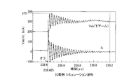
なお、このシミュレーションでは、直流電源21の電圧を300Vと仮定し、パワーモジュール本体部がオン状態の際のソース電流Isを200Aと仮定した。また、キャリア周波数(PWM制御の際、インバータで出力電圧のパルス幅を決めるための変調波の周波数)を100kHzと仮定した。また、比較例によるパワーモジュール本体部800aおよび800bの内部の配線インダクタンスを7.426nHと仮定するとともに、第1実施形態によるパワーモジュール本体部100aの内部の配線インダクタンスを3.0898nHと仮定した。なお、第1実施形態によるパワーモジュール本体部100aでは、1つのパワーモジュール本体部100aの内部にP側トランジスタ素子5a、P側ダイオード素子5b、N側トランジスタ素子6a、および、N側ダイオード素子6bが設けられる一方、比較例によるパワーモジュール本体部800aおよび800bでは、P側トランジスタ素子802およびP側ダイオード素子803と、N側トランジスタ素子804およびN側ダイオード素子805とが別個のパワーモジュール本体部に設けられている。このため、比較例によるパワーモジュール本体部800aおよび800bの内部の配線インダクタンスを、第1実施形態によるパワーモジュール本体部100aの内部の配線インダクタンスよりも大きくした。
図14は、比較例によるシミュレーションの結果を示している。縦軸は、電圧(V)と、ソース電流Is(A)を表わし、横軸は、時間を表わしている。そして、このシミュレーションにより、パワーモジュール本体部800aおよび800bをオン状態からオフ状態にした場合に、配線インダクタンスに蓄積されていたエネルギが、図13に示す閉回路(1点鎖線、LC回路)の中で共振した結果、サージ電圧が発生するとともに、リンギング(パルス状などの急峻な変化をする信号が、回路網を通過したときに生じる波状の波形)が発生することが判明した。
また、図15は、第1実施形態によるシミュレーションの結果を示している。そして、このシミュレーションにより、パワーモジュール本体部100aをオン状態からオフ状態にした場合に、配線インダクタンスに蓄積されていたエネルギが、図12に示す閉回路(1点鎖線、LC回路)の中で共振した結果、サージ電圧が発生するとともに、リンギングが発生することが判明した。なお、図14に示す比較例によるシミュレーションにおけるリンギングは、パワーモジュール本体部800aおよび800bがオフ状態にされてから、0.775μs(=239.2-238.425)後に終了した一方、図15に示す第1実施形態によるシミュレーションにおけるリンギングは、パワーモジュール本体部100aがオフ状態にされてから、0.3μs(=238.53-238.23)後に終了することが判明した。すなわち、示す第1実施形態によるシミュレーションにおけるリンギングの方が早く終了することが確認された。また、サージ電圧の最大値は、図14に示す比較例では、375Vになる一方、図15に示す第1実施形態では、339Vになることが判明した。すなわち、第1実施形態では、サージ電圧が減少することが確認された。これは、第1実施形態の配線インダクタンス(3.0898nH)が、比較例の配線インダクタンス(7.426nH)よりも小さいので、サージ電圧が減少したと考えられる。なお、第1実施形態(比較例)において、スナバコンデンサ13(808)を設けない場合では、サージ電圧の最大値は、比較例によるサージ電圧の最大値(375V)よりもさらに大きくなる。
第1実施形態では、上記のように、P側導電板3の表面上に配置されるP側半導体素子5と、第2N側導電板4bの表面上に配置され、P側半導体素子5と電気的に接続されるN側半導体素子6とをパワーモジュール本体部100aに設けることによって、P側半導体素子5とN側半導体素子6とが、それぞれ、異なる2つのパワーモジュール本体部に別個に設けられる場合と比べて、P側半導体素子5とN側半導体素子6との間の距離を小さくすることができるので、P側半導体素子5とN側半導体素子6との間の配線インダクタンスを小さくすることができる。また、パワーモジュール本体部100aの内部において、P側半導体素子5とN側半導体素子6との間にP側導電板3と第2N側導電板4bとに接続するようにスナバコンデンサ13を設けることによって、サージ電圧に起因するP側半導体素子5およびN側半導体素子6の破壊を抑制することができるとともに、スナバコンデンサ13がパワーモジュール本体部100aの外部の基板などに設けられる場合と比べて、P側半導体素子5およびN側半導体素子6とスナバコンデンサ13との間の距離が小さくなるので、P側半導体素子5およびN側半導体素子6とスナバコンデンサ13との間の配線インダクタンスを小さくすることができる。
また、第1実施形態では、上記のように、スナバコンデンサ13を、P側半導体素子5とN側半導体素子6との間にP側導電板3と第2N側導電板4bとに直接接続するように配置する。これにより、スナバコンデンサ13が配線などを介して配置される場合と比べて、スナバコンデンサ13とP側導電板3および第2N側導電板4bとの間の配線インダクタンスを小さくすることができる。
また、第1実施形態では、上記のように、スナバコンデンサ13を、P側半導体素子5とN側半導体素子6との間にP側導電板3と第2N側導電板4bとに跨るように配置する。これにより、スナバコンデンサ13とP側導電板3とを容易に直接接続することができるとともに、スナバコンデンサ13と第2N側導電板4bとを容易に直接接続することができる。
また、第1実施形態では、上記のように、P側半導体素子5のソース電極と、N側半導体素子6のドレイン電極とを互いに電気的に接続し、スナバコンデンサ13を、P側導電板3を介してP側半導体素子5のドレイン電極に電気的に接続するとともに、第2N側導電板4bを介してN側半導体素子6のソース電極に電気的に接続する。これにより、P側半導体素子5およびN側半導体素子6のスイッチング時に生じるサージ電圧を、スナバコンデンサ13により抑制することができる。
また、第1実施形態では、上記のように、パワーモジュール本体部100aが、P側導電板3の表面上に形成されるP側半導体素子5と、第1N側導電板4aの表面上に形成されるN側半導体素子6との表面上に形成され、上方に延びる柱状を有するとともに、柱状の上端面が略平坦に形成されている柱状電極7を含み、スナバコンデンサ13を、平面的に見て、柱状電極7に囲まれた領域に配置する。これにより、スナバコンデンサ13が柱状電極7に囲まれた領域の外に配置されている場合と異なり、パワーモジュール本体部100aが大きくなるのを抑制することができる。また、柱状電極7を上方に延びる柱状を有するとともに、柱状の上端面を略平坦に形成することにより、電極がたとえば細いワイヤ状である場合と異なり、配線インダクタンスを小さくすることができる。その結果、配線インダクタンスが大きいことに起因して、P側半導体素子5およびN側半導体素子6が高速に動作できなくなるのを抑制することができる。また、柱形状の柱状電極7により、細いワイヤー状の電極を用いる場合よりも放熱量を増加させることができるので、放熱性を向上させることができる。
また、第1実施形態では、上記のように、パワーモジュール本体部100aが、表面にP側導電板3、第1N側導電板4aおよび第2N側導電板4bが形成され、裏面に金属板1が形成される絶縁基板2を含み、スナバコンデンサ13を、P側導電板3と第2N側導電板4bとを直接接続するように配置する。これにより、P側導電板3、第1N側導電板4a、第2N側導電板4bおよびスナバコンデンサ13が、1つの絶縁基板2の表面上に形成されるので、P側導電板3、第1N側導電板4a、第2N側導電板4bおよびスナバコンデンサ13が、それぞれ、異なる絶縁基板に形成される場合と異なり、パワーモジュール本体部100aが大きくなるのを抑制することができる。
また、第1実施形態では、上記のように、スナバコンデンサ13を、パワーモジュール本体部100aの内部の配線基板200と反対側において、P側導電板3および第2N側導電板4bに直接接続するように配置する。これにより、スナバコンデンサ13が、P側導電板3および第2N側導電板4b側に配置されるので、スナバコンデンサ13と、P側導電板3および第2N側導電板4bとの間の距離が小さくなる。これにより、スナバコンデンサ13と、P側導電板3および第2N側導電板4bとの間の配線インダクタンスを小さくすることができる。
(第2実施形態)
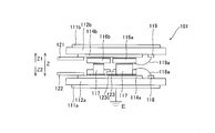
次に、図16~図20を参照して、第2実施形態のパワーモジュール本体部101について説明する。この第2実施形態では、上記1つの絶縁基板の表面上に、P側半導体素子とN側半導体素子とが設けられる上記第1実施形態と異なり、2つの絶縁基板に挟まれるようにP側半導体素子とN側半導体素子とが設けられている。
次に、図16~図20を参照して、第2実施形態のパワーモジュール本体部101について説明する。この第2実施形態では、上記1つの絶縁基板の表面上に、P側半導体素子とN側半導体素子とが設けられる上記第1実施形態と異なり、2つの絶縁基板に挟まれるようにP側半導体素子とN側半導体素子とが設けられている。
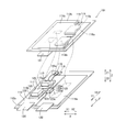
図16、図18~図20に示すように、パワーモジュール本体部101では、絶縁基板112aと絶縁基板112bとが対向するように配置されている。絶縁基板112aには、金属板111aと、絶縁基板112aと、P側導電板113と、第1N側導電板114aと、2つのP側半導体素子115と、2つの柱状電極117と、2つのP側制御端子118と、P側端子120と、N側端子122と、スナバコンデンサ123とが設けられている。また、金属板111aは、接地されている。なお、金属板111aは、本発明の「裏面側電極」の一例である。また、絶縁基板112aおよび絶縁基板112bは、それぞれ、本発明の「第1絶縁基板」および「第2絶縁基板」の一例である。また、P側導電板113は、本発明の「第1導電板」の一例である。また、第1N側導電板114aは、本発明の「第2導電板」の一例である。また、柱状電極117は、本発明の「電極用導体」の一例である。また、N側端子122は、本発明の「負側入出力端子」の一例である。また、スナバコンデンサ123は、本発明の「コンデンサ」の一例である。
また、図17~図20に示すように、パワーモジュール本体部101の絶縁基板112bには、金属板111bと、第2N側導電板114bと、2つのN側半導体素子116と、2つの柱状電極117と、2のN側制御端子119と、U相端子121とが設けられている。また、金属板111bは、上記金属板111aと異なり、接地(図18および図19参照)されない。これにより、金属板111aおよび金属板111bの両方が接地されている場合と異なり、U相端子121と接地(アース)との間の浮遊容量が小さくなる。その結果、コモンモードノイズを低減することが可能となる。
また、金属板111a、P側導電板113、第1N側導電板114a、金属板111bおよび第2N側導電板114bは、銅などの金属からなる。また、絶縁基板112aおよび112bは、セラミックなどの絶縁物からなる。このパワーモジュール本体部101では、金属板111a、絶縁基板112aおよびP側導電板113により、P側の絶縁回路基板が構成され、金属板111a、絶縁基板112a、第1N側導電板114aにより、N側の絶縁回路基板が構成されている。また、金属板111b、絶縁基板112b、第2N側導電板114bにより、N側の絶縁回路基板が構成されている。なお、P側半導体素子115は、本発明の「第1電力変換用半導体素子」の一例である。また、N側半導体素子116は、本発明の「第2電力変換用半導体素子」の一例である。
図16に示すように、2つのP側半導体素子115は、1つのP側トランジスタ素子115aと、1つのP側ダイオード素子115bとにより構成されている。このP側トランジスタ素子115aは、たとえば、MOSFET(電界効果型トランジスタ)である。また、P側ダイオード素子115bは、たとえば、SBD(ショットキーバリアダイオード)である。なお、P側ダイオード素子115bは、還流ダイオードとしての機能を有する。図11に示す上記第1実施形態と同様に、P側トランジスタ素子115aと、P側ダイオード素子115bとは、電気的に並列に接続されている。具体的には、P側ダイオード素子115bのカソード電極は、P側トランジスタ素子115aのドレイン電極に電気的に接続されている。また、P側ダイオード素子115bのアノード電極は、P側トランジスタ素子115aのソース電極に電気的に接続されている。なお、P側トランジスタ素子115aは、本発明の「電圧駆動型トランジスタ素子」の一例である。また、P側ダイオード素子115bは、本発明の「還流ダイオード素子」の一例である。
P側トランジスタ素子115aのドレイン電極およびP側ダイオード素子115bのカソード電極は、P側導電板113に電気的に接続されている。図20に示すように、P側トランジスタ素子115aおよびP側ダイオード素子115bの下面(矢印Z2方向側の面)は、半田からなる接合材125を介してP側導電板113の上面(矢印Z1方向側の面)に接合されている。なお、P側トランジスタ素子115aおよびP側ダイオード素子115bは、P側導電板113の表面においてY方向に所定の間隔を隔てて並んで配置されている。また、P側トランジスタ素子115aは、P側ダイオード素子115bよりも矢印Y2方向側に配置されている。なお、半田からなる接合材125の代わりに、Agナノペーストからなる接合材を用いてもよい。
同様に、図17に示すように、2つのN側半導体素子116は、1つのN側トランジスタ素子116aと、1つのN側ダイオード素子116bとにより構成されている。このN側ダイオード素子116bは、還流ダイオードとしての機能を有する。図11に示す上記第1実施形態と同様に、N側トランジスタ素子116aと、N側ダイオード素子116bとは、電気的に並列に接続されている。具体的には、N側ダイオード素子116bのカソード電極は、N側トランジスタ素子116aのドレイン電極に電気的に接続されている。また、N側ダイオード素子116bのアノード電極は、N側トランジスタ素子116aのソース電極に電気的に接続されている。なお、N側トランジスタ素子116aは、本発明の「電圧駆動型トランジスタ素子」の一例である。また、N側ダイオード素子116bは、本発明の「還流ダイオード素子」の一例である。
図20に示すように、N側トランジスタ素子116aおよびN側ダイオード素子116bは、第2N側導電板114bの上面(矢印Z2方向側の面)においてY方向に並んで配置されている。また、N側トランジスタ素子116aは、N側ダイオード素子116bよりも矢印Y2方向側に配置されている。なお、絶縁基板112aと絶縁基板112bとが対向するように配置された状態では、P側トランジスタ素子115aおよびN側トランジスタ素子116aと、P側ダイオード素子115bおよびN側ダイオード素子116bとは、それぞれ、X方向に並んで配置されている。また、P側トランジスタ素子115aおよびP側ダイオード素子115bは、N側トランジスタ素子116aおよびN側ダイオード素子116bよりも矢印X1方向側に配置されている。
図16に示すように、2つのP側制御端子118は、それぞれ、P側トランジスタ素子115aの上面(矢印Z1方向側の面)に設けられたゲート電極およびソース電極に対してワイヤボンディングによりワイヤ118aを介して接続されている。同様に、図17に示すように、2つのN側制御端子119は、それぞれ、N側トランジスタ素子116aの上面に設けられたゲート電極およびソース電極に対してワイヤボンディングによりワイヤ119aを介して接続されている。
図16に示すように、P側端子120は、P側導電板113の上面(矢印Z1方向側の面)に接合されるように構成されている。また、P側端子120は、P側導電板113を介してP側トランジスタ素子115aのドレイン電極およびP側ダイオード素子115bのカソード電極に電気的に接続されるように構成されている。なお、P側端子120は、X方向およびY方向に延びる平板状に形成されている。
また、N側端子122は、第1N側導電板114aの上面(矢印Z1方向側の面)に接合されるように構成されている。また、N側端子122は、絶縁基板112aと絶縁基板112bとが対向するように配置された状態では、第1N側導電板114aを介してN側トランジスタ素子116aのソース電極およびN側ダイオード素子116bのアノード電極に電気的に接続されるように構成されている。なお、N側端子122は、X方向およびY方向に延びる平板状に形成されている。
図17に示すように、U相端子121は、第2N側導電板114bの上面(矢印Z2方向側の面)に接合されるように構成されている。また、U相端子121は、第2N側導電板114bを介してN側トランジスタ素子116aのドレイン電極およびN側ダイオード素子116bのカソード電極に電気的に接続されるように構成されている。なお、U相端子121は、X方向およびY方向に延びる平板状に形成されている。
また、P側端子120、N側端子122およびU相端子121は、図示しない配線基板との電気的接続をとるために設けられている。また、これらのP側端子120、N側端子122およびU相端子121は、パワーモジュール本体部101と配線基板との間で流入および流出する電流の流入口および流出口として機能する。
ここで、第2実施形態では、図16に示すように、絶縁基板112a側に設けられるP側導電板113と第1N側導電板114aとに配線を介さずに直接接続するようにスナバコンデンサ123が配置されている。また、スナバコンデンサ123は、P側導電板113と第1N側導電板114aとに跨るように配置されている。なお、スナバコンデンサ123の矢印X1方向の端部、および、矢印X2方向の端部には、それぞれ、電極123aが設けられている。また、スナバコンデンサ123の電極123aの間の部分123bは、セラミックから構成されている。そして、電極123aと、P側導電板113および第1N側導電板114aとが半田123cにより接合されている。これにより、絶縁基板112aと絶縁基板112bとが対向するように配置された状態では、スナバコンデンサ123は、P側トランジスタ素子115aのドレイン電極と、N側トランジスタ素子116aのソース電極に電気的に接続される。また、スナバコンデンサ123は、P側ダイオード素子115bのカソード電極と、N側ダイオード素子116bのアノード電極に電気的に接続される。なお、パワーモジュール本体部101は、U相の電力変換が行われる。また、V相、W相の電力変換を行うパワーモジュール本体部もパワーモジュール本体部101と略同様の構成を有している。
第2実施形態では、上記のように、パワーモジュール本体部101が、表面にP側導電板113および第1N側導電板114aが形成され、裏面に金属板111aが形成される絶縁基板112aと、絶縁基板112bとの間にP側半導体素子115およびN側半導体素子116を挟んで絶縁基板112aに対向するように配置される絶縁基板112bとを含み、スナバコンデンサ123を、絶縁基板112a側において、P側導電板113と第1N側導電板114aとに直接接続するように配置する。これにより、スナバコンデンサ123が、P側導電板113および第1N側導電板114a側に配置されるので、スナバコンデンサ123と、P側導電板113および第1N側導電板114aとの間の距離が小さくなる。これにより、スナバコンデンサ123と、P側導電板113および第1N側導電板114aとの間の配線インダクタンスを小さくすることができる。
なお、今回開示された実施形態は、すべての点で例示であって制限的なものではないと考えられるべきである。本発明の範囲は、上記した実施形態の説明ではなく特許請求の範囲によって示され、さらに特許請求の範囲と均等の意味および範囲内でのすべての変更が含まれる。
たとえば、上記第1および第2実施形態では、本発明の電力変換用半導体素子としてMOSFET(電界効果型トランジスタ)およびSBD(ショットキーバリアダイオード)を用いる例を示したが、本発明はこれに限らない。本発明では、電力変換用半導体素子であれば、MOSFETおよびSBD以外の半導体素子を用いてもよい。
また、上記第1および第2実施形態では、本発明の電圧駆動型トランジスタとしてMOSFETを用いる例を示したが、本発明はこれに限らない。本発明では、電圧駆動型トランジスタであれば、IGBT(絶縁ゲートバイポーラトランジスタ)などのその他のトランジスタを用いてもよい。
また、上記第1および第2実施形態では、還流ダイオードとして、SBDを用いる例を示したが、本発明はこれに限らない。本発明では、還流ダイオードであれば、FRD(ファーストリカバリーダイオード)などのその他のダイオードを用いてもよい。
また、上記第1および第2実施形態では、パワーモジュール本体部のP側およびN側のそれぞれに、MOSFETとSBDとを1セットずつ配置する例を示したが、本発明はこれに限らない。本発明では、パワーモジュール本体部のP側およびN側のそれぞれに、MOSFETとSBDとを複数セットずつ配置してもよい。
また、上記第1および第2実施形態では、P側導電板および第1N側導電板に配線を介さずに直接半田により接続するようにスナバコンデンサが配置される例を示したが、本発明はこれに限らない。本発明では、スナバコンデンサは、パワーモジュール本体部の内部に設けられていればよい。たとえば、スナバコンデンサを、短い配線を介してP側導電板および第1N側導電板との間にP側導電板および第1N側導電板と接続するようにしてもよい。
1、111a 金属板(裏面側電極板)
2 絶縁基板
3、113 P側導電板(第1導電板)
4a 第1N側導電板(第2導電板、素子側第2導電板)
4b 第2N側導電板(第2導電板、端子側第2導電板)
5、115 P側半導体素子(第1電力変換用半導体素子)
5a、115a P側トランジスタ素子(電圧駆動型トランジスタ素子)
5b、115b P側ダイオード素子(還流ダイオード素子)
6、116 N側半導体素子(第2電力変換用半導体素子)
6a、116a P側トランジスタ素子(電圧駆動型トランジスタ素子)
6b、116b P側ダイオード素子(還流ダイオード素子)
7、117 柱状電極(電極用導体)
12、122 N側端子(負側入力端子)
13、123 スナバコンデンサ(コンデンサ)
100 パワーモジュール(電力変換装置)
100a、100b、100c、101 パワーモジュール本体部(電力変換装置本体部)
112a 絶縁基板(第1絶縁基板)
112b 絶縁基板(第2絶縁基板)
114a 第1N側導電板(第2導電板)
200 配線基板
2 絶縁基板
3、113 P側導電板(第1導電板)
4a 第1N側導電板(第2導電板、素子側第2導電板)
4b 第2N側導電板(第2導電板、端子側第2導電板)
5、115 P側半導体素子(第1電力変換用半導体素子)
5a、115a P側トランジスタ素子(電圧駆動型トランジスタ素子)
5b、115b P側ダイオード素子(還流ダイオード素子)
6、116 N側半導体素子(第2電力変換用半導体素子)
6a、116a P側トランジスタ素子(電圧駆動型トランジスタ素子)
6b、116b P側ダイオード素子(還流ダイオード素子)
7、117 柱状電極(電極用導体)
12、122 N側端子(負側入力端子)
13、123 スナバコンデンサ(コンデンサ)
100 パワーモジュール(電力変換装置)
100a、100b、100c、101 パワーモジュール本体部(電力変換装置本体部)
112a 絶縁基板(第1絶縁基板)
112b 絶縁基板(第2絶縁基板)
114a 第1N側導電板(第2導電板)
200 配線基板
Claims (9)
- 電力変換装置本体部を備え、
前記電力変換装置本体部は、
前記電力変換装置本体部内に間隔を隔てて配置された第1導電板および第2導電板と、
前記第1導電板の表面上に配置される第1電力変換用半導体素子と、
前記第2導電板の表面上に配置され、前記第1電力変換用半導体素子と電気的に接続される第2電力変換用半導体素子と、
前記電力変換装置本体部の内部において、前記第1電力変換用半導体素子と前記第2電力変換用半導体素子との間に前記第1導電板と前記第2導電板とに接続するように配置され、サージ電圧を抑制するためのコンデンサとを含む、電力変換装置。 - 前記コンデンサは、前記第1電力変換用半導体素子と前記第2電力変換用半導体素子との間に前記第1導電板と前記第2導電板とに直接接続するように配置されている、請求項1に記載の電力変換装置。
- 前記コンデンサは、前記第1電力変換用半導体素子と前記第2電力変換用半導体素子との間に前記第1導電板と前記第2導電板とに跨るように配置されている、請求項1または2に記載の電力変換装置。
- 前記第1電力変換用半導体素子の一方電極と、前記第2電力変換用半導体素子の一方電極とが互いに電気的に接続され、
前記コンデンサは、前記第1導電板を介して前記第1電力変換用半導体素子の他方電極に電気的に接続されるとともに、前記第2導電板を介して前記第2電力変換用半導体素子の他方電極に電気的に接続されている、請求項1~3のいずれか1項に記載の電力変換装置。 - 前記電力変換装置本体部は、表面に前記第1導電板および前記第2導電板が形成され、裏面に裏面側導電板が形成される絶縁基板をさらに含み、
前記第2導電板は、前記第2電力変換用半導体素子が形成される素子側第2導電板と、負側入出力端子が形成される端子側第2導電板とを含み、
前記コンデンサは、前記第1導電板と前記端子側第2導電板とに直接接続するように配置されている、請求項1~4のいずれか1項に記載の電力変換装置。 - 前記第1電力変換用半導体素子および前記第2電力変換用半導体素子の前記第1導電板および前記第2導電板とは反対側において、前記第1電力変換用半導体素子および前記第2電力変換用半導体素子に電気的に接続される配線基板をさらに備え、
前記コンデンサは、前記電力変換装置本体部の内部の前記配線基板と反対側において、前記第1導電板および前記第2導電板に直接接続するように配置されている、請求項5に記載の電力変換装置。 - 前記電力変換装置本体部は、
表面に前記第1導電板および前記第2導電板が形成され、裏面に裏面側導電板が形成される第1絶縁基板と、
前記第1絶縁基板との間に前記第1電力変換用半導体素子および前記第2電力変換用半導体素子を挟んで前記第1絶縁基板に対向するように配置される第2絶縁基板とをさらに含み、
前記コンデンサは、前記第1絶縁基板側において、前記第1導電板と前記第2導電板とに直接接続するように配置されている、請求項1~4のいずれか1項に記載の電力変換装置。 - 前記第1電力変換用半導体素子および前記第2電力変換用半導体素子は、電圧駆動型トランジスタ素子を含み、
前記コンデンサは、前記電力変換装置本体部の内部において、前記第1導電板に形成される前記電圧駆動型トランジスタ素子と前記第2導電板に形成される前記電圧駆動型トランジスタ素子との間に前記第1導電板と前記第2導電板とに直接接続するように配置されている、請求項1~7のいずれか1項に記載の電力変換装置。 - 前記第1電力変換用半導体素子および前記第2電力変換用半導体素子は、前記電圧駆動型トランジスタ素子に並列接続される還流ダイオード素子を含み、
前記コンデンサは、前記電力変換装置本体部の内部において、前記第1導電板に形成される前記還流ダイオード素子と前記第2導電板に形成される前記還流ダイオード素子との間に前記第1導電板と前記第2導電板とに直接接続するように配置されている、請求項8に記載の電力変換装置。
Priority Applications (3)
| Application Number | Priority Date | Filing Date | Title |
|---|---|---|---|
| JP2012546717A JP5568645B2 (ja) | 2010-12-01 | 2011-09-05 | 電力変換装置 |
| CN201180057839.3A CN103238269B (zh) | 2010-12-01 | 2011-09-05 | 电力变换装置 |
| US13/905,132 US20130258736A1 (en) | 2010-12-01 | 2013-05-30 | Power converter |
Applications Claiming Priority (2)
| Application Number | Priority Date | Filing Date | Title |
|---|---|---|---|
| JP2010-268744 | 2010-12-01 | ||
| JP2010268744 | 2010-12-01 |
Related Child Applications (1)
| Application Number | Title | Priority Date | Filing Date |
|---|---|---|---|
| US13/905,132 Continuation US20130258736A1 (en) | 2010-12-01 | 2013-05-30 | Power converter |
Publications (1)
| Publication Number | Publication Date |
|---|---|
| WO2012073571A1 true WO2012073571A1 (ja) | 2012-06-07 |
Family
ID=46171527
Family Applications (1)
| Application Number | Title | Priority Date | Filing Date |
|---|---|---|---|
| PCT/JP2011/070126 Ceased WO2012073571A1 (ja) | 2010-12-01 | 2011-09-05 | 電力変換装置 |
Country Status (4)
| Country | Link |
|---|---|
| US (1) | US20130258736A1 (ja) |
| JP (2) | JP5568645B2 (ja) |
| CN (1) | CN103238269B (ja) |
| WO (1) | WO2012073571A1 (ja) |
Cited By (6)
| Publication number | Priority date | Publication date | Assignee | Title |
|---|---|---|---|---|
| JP2014176290A (ja) * | 2013-03-11 | 2014-09-22 | Semiconductor Components Industries Llc | スイッチング素子、整流素子、および電荷蓄積素子を含む回路 |
| JP2016013027A (ja) * | 2014-06-30 | 2016-01-21 | 富士電機株式会社 | 電力変換装置及び電動モータ |
| JP2016535513A (ja) * | 2013-10-31 | 2016-11-10 | エルジー エレクトロニクス インコーポレイティド | 無線通信システムにおける端末により実行されるセル再選択方法及び前記方法を利用する端末 |
| JP2018195694A (ja) * | 2017-05-17 | 2018-12-06 | 株式会社Soken | 電力変換器 |
| US10418895B2 (en) | 2014-10-30 | 2019-09-17 | Rohm Co., Ltd. | Power module and power circuit |
| WO2022091633A1 (ja) * | 2020-10-30 | 2022-05-05 | 日立Astemo株式会社 | パワー半導体装置、電力変換装置、および電動システム |
Families Citing this family (18)
| Publication number | Priority date | Publication date | Assignee | Title |
|---|---|---|---|---|
| JP5963912B1 (ja) * | 2015-05-14 | 2016-08-03 | 三菱電機株式会社 | 半導体モジュール |
| US9906213B2 (en) | 2015-11-06 | 2018-02-27 | Globalfoundries Inc. | Reducing thermal runaway in inverter devices |
| JP6584333B2 (ja) * | 2016-01-28 | 2019-10-02 | 三菱電機株式会社 | パワーモジュール |
| FR3050571A1 (fr) * | 2016-04-20 | 2017-10-27 | Centre Nat Rech Scient | Convertisseur electronique de puissance utilisant deux puces multi-poles de puissance a substrats complementaires n et p. |
| US10122357B2 (en) * | 2016-11-14 | 2018-11-06 | Ford Global Technologies, Llc | Sensorless temperature compensation for power switching devices |
| JP6274380B1 (ja) * | 2016-11-24 | 2018-02-07 | 住友電気工業株式会社 | 半導体モジュール |
| WO2018096734A1 (ja) * | 2016-11-24 | 2018-05-31 | 住友電気工業株式会社 | 半導体モジュール |
| US11183485B2 (en) | 2016-11-24 | 2021-11-23 | Sumitomo Electric Industries, Ltd. | Semiconductor module |
| JP6601776B2 (ja) * | 2017-01-31 | 2019-11-06 | パナソニックIpマネジメント株式会社 | スイッチング電源装置 |
| JP6786416B2 (ja) * | 2017-02-20 | 2020-11-18 | 株式会社東芝 | 半導体装置 |
| JP6195691B1 (ja) * | 2017-02-21 | 2017-09-13 | 三菱電機株式会社 | 電力変換装置及びパワーモジュール |
| FR3073978B1 (fr) | 2017-11-17 | 2022-10-28 | Inst Vedecom | Module electronique de puissance et systeme electronique comprenant un tel module electronique |
| EP3761357A1 (en) * | 2019-07-04 | 2021-01-06 | Infineon Technologies Austria AG | Semiconductor device |
| JP7356402B2 (ja) * | 2020-05-18 | 2023-10-04 | 日立Astemo株式会社 | パワーモジュール |
| DE112020007394T5 (de) * | 2020-07-08 | 2023-04-20 | Mitsubishi Electric Corporation | Leistungshalbleitermodul und stromrichtervorrichtung |
| CN116780913A (zh) | 2022-03-11 | 2023-09-19 | 通用汽车环球科技运作有限责任公司 | 用于车辆的逆变器模块 |
| DE102022202898B4 (de) | 2022-03-24 | 2024-09-12 | Zf Friedrichshafen Ag | Leistungshalbleitermodul mit zwei gegenüberliegenden halb-brücken |
| US20250253216A1 (en) * | 2024-02-07 | 2025-08-07 | Tesla, Inc. | Semiconductor package design with terminals for connecting to external capacitor |
Citations (4)
| Publication number | Priority date | Publication date | Assignee | Title |
|---|---|---|---|---|
| JPH0614562A (ja) * | 1992-06-29 | 1994-01-21 | Fuji Electric Co Ltd | スナバ回路 |
| JP2007053295A (ja) * | 2005-08-19 | 2007-03-01 | Hitachi Ltd | 半導体装置,それを用いた電力変換装置及び車載用電機システム |
| WO2007094162A1 (ja) * | 2006-02-17 | 2007-08-23 | Kabushiki Kaisha Yaskawa Denki | バスバーを備えた電力変換装置 |
| JP2009225612A (ja) * | 2008-03-18 | 2009-10-01 | Mitsubishi Electric Corp | パワーモジュール |
Family Cites Families (9)
| Publication number | Priority date | Publication date | Assignee | Title |
|---|---|---|---|---|
| JP3271059B2 (ja) * | 1998-05-25 | 2002-04-02 | 株式会社日立製作所 | 電気車用3相インバータ装置 |
| US6995473B2 (en) * | 2002-12-19 | 2006-02-07 | Matsushita Electric Industrial Co., Ltd. | Stacked semiconductor transistors |
| JP2007235004A (ja) * | 2006-03-03 | 2007-09-13 | Mitsubishi Electric Corp | 半導体装置 |
| EP2051301A4 (en) * | 2006-08-09 | 2010-06-16 | Honda Motor Co Ltd | SEMICONDUCTOR COMPONENT |
| JP4905254B2 (ja) * | 2007-05-25 | 2012-03-28 | トヨタ自動車株式会社 | コンデンサ一体バスバーの製造方法 |
| JP2009219268A (ja) * | 2008-03-11 | 2009-09-24 | Daikin Ind Ltd | 電力変換装置 |
| JP5212088B2 (ja) * | 2008-12-25 | 2013-06-19 | 株式会社デンソー | 半導体モジュール冷却装置 |
| JP5287359B2 (ja) * | 2009-03-04 | 2013-09-11 | 株式会社デンソー | 半導体モジュール |
| US8178954B2 (en) * | 2009-07-31 | 2012-05-15 | Alpha & Omega Semiconductor, Inc. | Structure of mixed semiconductor encapsulation structure with multiple chips and capacitors |
-
2011
- 2011-09-05 JP JP2012546717A patent/JP5568645B2/ja not_active Expired - Fee Related
- 2011-09-05 WO PCT/JP2011/070126 patent/WO2012073571A1/ja not_active Ceased
- 2011-09-05 CN CN201180057839.3A patent/CN103238269B/zh not_active Expired - Fee Related
-
2013
- 2013-05-30 US US13/905,132 patent/US20130258736A1/en not_active Abandoned
-
2014
- 2014-06-23 JP JP2014128382A patent/JP2014187874A/ja active Pending
Patent Citations (4)
| Publication number | Priority date | Publication date | Assignee | Title |
|---|---|---|---|---|
| JPH0614562A (ja) * | 1992-06-29 | 1994-01-21 | Fuji Electric Co Ltd | スナバ回路 |
| JP2007053295A (ja) * | 2005-08-19 | 2007-03-01 | Hitachi Ltd | 半導体装置,それを用いた電力変換装置及び車載用電機システム |
| WO2007094162A1 (ja) * | 2006-02-17 | 2007-08-23 | Kabushiki Kaisha Yaskawa Denki | バスバーを備えた電力変換装置 |
| JP2009225612A (ja) * | 2008-03-18 | 2009-10-01 | Mitsubishi Electric Corp | パワーモジュール |
Cited By (8)
| Publication number | Priority date | Publication date | Assignee | Title |
|---|---|---|---|---|
| JP2014176290A (ja) * | 2013-03-11 | 2014-09-22 | Semiconductor Components Industries Llc | スイッチング素子、整流素子、および電荷蓄積素子を含む回路 |
| JP2016535513A (ja) * | 2013-10-31 | 2016-11-10 | エルジー エレクトロニクス インコーポレイティド | 無線通信システムにおける端末により実行されるセル再選択方法及び前記方法を利用する端末 |
| JP2016013027A (ja) * | 2014-06-30 | 2016-01-21 | 富士電機株式会社 | 電力変換装置及び電動モータ |
| US10418895B2 (en) | 2014-10-30 | 2019-09-17 | Rohm Co., Ltd. | Power module and power circuit |
| JP2018195694A (ja) * | 2017-05-17 | 2018-12-06 | 株式会社Soken | 電力変換器 |
| WO2022091633A1 (ja) * | 2020-10-30 | 2022-05-05 | 日立Astemo株式会社 | パワー半導体装置、電力変換装置、および電動システム |
| JP2022073334A (ja) * | 2020-10-30 | 2022-05-17 | 日立Astemo株式会社 | パワー半導体装置、電力変換装置、および電動システム |
| US12581947B2 (en) | 2020-10-30 | 2026-03-17 | Hitachi Astemo, Ltd. | Power semiconductor device, power conversion device, and electric system |
Also Published As
| Publication number | Publication date |
|---|---|
| US20130258736A1 (en) | 2013-10-03 |
| JP5568645B2 (ja) | 2014-08-06 |
| CN103238269B (zh) | 2015-06-24 |
| CN103238269A (zh) | 2013-08-07 |
| JP2014187874A (ja) | 2014-10-02 |
| JPWO2012073571A1 (ja) | 2014-05-19 |
Similar Documents
| Publication | Publication Date | Title |
|---|---|---|
| JP5568645B2 (ja) | 電力変換装置 | |
| JP6288301B2 (ja) | ハーフブリッジパワー半導体モジュール及びその製造方法 | |
| JP6245365B2 (ja) | ハーフブリッジパワー半導体モジュール及びその製造方法 | |
| JP4277169B2 (ja) | 電力用半導体モジュール | |
| US10163868B2 (en) | Semiconductor device | |
| CN102856308B (zh) | 功率半导体模块 | |
| CN103296016B (zh) | 半导体模块 | |
| JP6603676B2 (ja) | ハーフブリッジパワー半導体モジュール及びその製造方法 | |
| JP2015126342A (ja) | パワー回路およびパワーモジュール | |
| JP2011097053A (ja) | インダクタンスを低減した電力モジュール組立体 | |
| CN104081646A (zh) | 电力变换装置和用于制造电力变换装置的方法 | |
| US9773767B2 (en) | Semiconductor device | |
| KR20180073474A (ko) | 반도체 장치 및 인버터 시스템 | |
| JP6331543B2 (ja) | ハーフブリッジパワー半導体モジュール及びその製造方法 | |
| JP7010036B2 (ja) | 半導体モジュール | |
| JP2017162884A (ja) | 半導体装置 | |
| JP4479365B2 (ja) | 半導体装置 | |
| JP3947669B2 (ja) | 半導体構成部品 |
Legal Events
| Date | Code | Title | Description |
|---|---|---|---|
| 121 | Ep: the epo has been informed by wipo that ep was designated in this application |
Ref document number: 11844268 Country of ref document: EP Kind code of ref document: A1 |
|
| ENP | Entry into the national phase |
Ref document number: 2012546717 Country of ref document: JP Kind code of ref document: A |
|
| NENP | Non-entry into the national phase |
Ref country code: DE |
|
| 122 | Ep: pct application non-entry in european phase |
Ref document number: 11844268 Country of ref document: EP Kind code of ref document: A1 |