WO2012043164A1 - 熱式流量センサ - Google Patents
熱式流量センサ Download PDFInfo
- Publication number
- WO2012043164A1 WO2012043164A1 PCT/JP2011/070222 JP2011070222W WO2012043164A1 WO 2012043164 A1 WO2012043164 A1 WO 2012043164A1 JP 2011070222 W JP2011070222 W JP 2011070222W WO 2012043164 A1 WO2012043164 A1 WO 2012043164A1
- Authority
- WO
- WIPO (PCT)
- Prior art keywords
- flow sensor
- thermal flow
- heating resistor
- resistor
- thermal
- Prior art date
Links
Images


Classifications
-
- G—PHYSICS
- G01—MEASURING; TESTING
- G01F—MEASURING VOLUME, VOLUME FLOW, MASS FLOW OR LIQUID LEVEL; METERING BY VOLUME
- G01F1/00—Measuring the volume flow or mass flow of fluid or fluent solid material wherein the fluid passes through a meter in a continuous flow
- G01F1/68—Measuring the volume flow or mass flow of fluid or fluent solid material wherein the fluid passes through a meter in a continuous flow by using thermal effects
- G01F1/684—Structural arrangements; Mounting of elements, e.g. in relation to fluid flow
- G01F1/688—Structural arrangements; Mounting of elements, e.g. in relation to fluid flow using a particular type of heating, cooling or sensing element
- G01F1/69—Structural arrangements; Mounting of elements, e.g. in relation to fluid flow using a particular type of heating, cooling or sensing element of resistive type
-
- G—PHYSICS
- G01—MEASURING; TESTING
- G01F—MEASURING VOLUME, VOLUME FLOW, MASS FLOW OR LIQUID LEVEL; METERING BY VOLUME
- G01F1/00—Measuring the volume flow or mass flow of fluid or fluent solid material wherein the fluid passes through a meter in a continuous flow
- G01F1/68—Measuring the volume flow or mass flow of fluid or fluent solid material wherein the fluid passes through a meter in a continuous flow by using thermal effects
- G01F1/684—Structural arrangements; Mounting of elements, e.g. in relation to fluid flow
- G01F1/6845—Micromachined devices
-
- G—PHYSICS
- G01—MEASURING; TESTING
- G01F—MEASURING VOLUME, VOLUME FLOW, MASS FLOW OR LIQUID LEVEL; METERING BY VOLUME
- G01F1/00—Measuring the volume flow or mass flow of fluid or fluent solid material wherein the fluid passes through a meter in a continuous flow
- G01F1/68—Measuring the volume flow or mass flow of fluid or fluent solid material wherein the fluid passes through a meter in a continuous flow by using thermal effects
- G01F1/684—Structural arrangements; Mounting of elements, e.g. in relation to fluid flow
- G01F1/688—Structural arrangements; Mounting of elements, e.g. in relation to fluid flow using a particular type of heating, cooling or sensing element
- G01F1/69—Structural arrangements; Mounting of elements, e.g. in relation to fluid flow using a particular type of heating, cooling or sensing element of resistive type
- G01F1/692—Thin-film arrangements
Definitions
- the present invention relates to a thermal flow sensor for measuring a flow rate by installing a heating resistor in a fluid to be measured, and more particularly to a thermal flow sensor suitable for measuring an intake air flow rate and an exhaust gas flow rate of an internal combustion engine of an automobile.
- a thermal air flow sensor capable of directly measuring a mass flow rate has become mainstream.
- a sensor element of a thermal flow meter on a semiconductor substrate such as silicon (Si) using a micromachine technique.
- a cavity is formed by removing a part of a semiconductor substrate in a rectangular shape, and a heating resistor is formed on an electrical insulating film having a thickness of several microns formed in the cavity.
- a temperature sensing resistor is formed in the vicinity of the heating resistor, and the flow rate is measured based on the amount of heat transferred from the fluid to be measured flowing on the heating resistor to the temperature sensing resistor.
- the size of the heating resistor is as small as several hundred microns, and is formed into a thin film of several microns, so that the heat capacity is small and high-speed response and low power consumption are possible.
- the sensor element in order to reduce the contamination of the sensor element, the sensor element is arranged in a passage that takes in a part of the air flow, and oil or dust is removed from the sensor element using an inertial effect by bending the passage into various shapes. There is a method of taking a structure that is difficult to collide with.
- the present invention has been made in view of the above problems, and the object of the present invention is to provide an air flow without reducing the structural strength of the heating resistor when mounted on an internal combustion engine such as an automobile.
- An object of the present invention is to provide a thermal flow sensor that is small in size, low in power consumption, and high in accuracy by reducing a change in detection sensitivity of a sensor element due to a minute change in direction to reduce a flow measurement error.
- the thermal flow sensor of the present invention includes a heat resistance in a first region composed of one side on the electrode part side of the heating resistor and one side on the electrode part side of the front diaphragm part, and a heating resistor.
- the thermal resistance is adjusted so that the thermal resistance of the second region composed of the other side facing the one side and the other side facing the one side of the hollow portion is substantially equal.
- a flow rate measurement error is reduced by reducing a change in detection sensitivity of a sensor element due to a minute change in the air flow direction, and a small, low power consumption and high accuracy thermal flow sensor is provided. can do.
- FIG. An example of a sensor element mounting form. Configuration of sensor element before application of the present invention. YY 'cross-sectional structure and temperature distribution of the sensor element before application of the present invention. The relationship figure of the thermal resistance of the area
- YY 'cross-sectional structure and temperature distribution of the sensor element in the fourth embodiment The YY 'cross-section structure and temperature distribution of the sensor element in 5th Example.
- the top view of the sensor element in 6th Example The top view of the sensor element in 7th Example.
- XX 'cross-sectional structure and temperature distribution of the sensor element in 7th Example The detection circuit structure of the thermal type flow sensor in a 7th example.
- Example 1 A first embodiment according to the present invention will be described below.
- a semiconductor substrate 1 constituting a sensor element is made of a material having good thermal conductivity such as silicon (Si) or ceramic. Then, an electrical insulating film 3 a is formed on the semiconductor substrate 1, and the cavity 2 is formed by etching the semiconductor substrate 1 from the back surface to form the diaphragm 2. On the surface of the electrical insulating film 3 a on the diaphragm 2, a heating resistor 4 and a wiring portion 5 for energizing the heating resistor 4 are formed.
- the heating resistor 4 extends from the end of the short side of the cavity 2 on the side where the wiring part 5 is formed to the wiring part side end of the heating resistor 4 in the YY ′ line direction.
- the heating resistance is at a position where L1> L2. Place the body 4. Further, the heating resistor 4 is disposed in the center of the diaphragm 2 in the direction of the XX ′ line.
- upstream side temperature sensitive resistors 6a and 6b and downstream side temperature sensitive resistors 7a and 7b are formed on both sides of the heating resistor 4.
- the upstream temperature sensitive resistors 6a and 6b are arranged upstream of the heat generating resistor 4 in the fluid flow direction, and the downstream temperature sensitive resistors 7a and 7b are arranged in the fluid flow direction with respect to the heat generating resistor 4.
- the outermost surface of the sensor element is covered with an electrical insulating film 3b, and the electrical insulating film 3b serves as a protective film in addition to performing electrical insulation.
- the heating resistor 4 the upstream temperature sensing resistors 6 a and 6 b, and the downstream temperature sensing resistor 7 are provided.
- Lead wiring portions 8, 9, and 10 and electrode pad portions 11 are provided for connecting the resistors constituting a and 7b to the drive / detection circuit.
- the electrode pad portion 11 is formed of aluminum (Al) or the like.
- the heat generating resistor 4, the upstream temperature sensitive resistors 6a and 6b, and the downstream temperature sensitive resistors 7a and 7b are formed of a material having a relatively large resistance temperature coefficient whose resistance value varies with temperature.
- a semiconductor material such as polycrystalline silicon or single crystal silicon doped with impurities, or a metal material such as platinum (Pt), molybdenum (Mo), tungsten (W), or nickel alloy may be used.
- the electrical insulating films 3a and 3b are formed in a thin film shape with a thickness of about 2 microns from silicon dioxide (SiO 2 ) or silicon nitride (Si 3 N 4 ) so that a sufficient thermal insulation effect can be obtained.
- the heating resistor 4 is a main part of the heat generation on the diaphragm 2, and even if it is electrically connected to the heating resistor 4, the unit length can be increased by increasing the wiring width like the wiring part 5. A portion where the resistance value per unit is reduced or a portion which does not serve as a current path such as a projection formed from the heating resistor 4 is not included in the range of the heating resistor 4.
- the resistance value per unit length of the heating resistor 4 is desirably 10 times or more larger than the resistance value per unit length of the wiring portion 5.
- a semiconductor such as single crystal silicon is used as the semiconductor substrate 1.
- silicon dioxide and silicon nitride to form an electric insulating film 3a having a predetermined thickness of about 1 ⁇ m are formed by thermal oxidation or CVD.
- a polycrystalline silicon semiconductor thin film having a thickness of about 1 ⁇ m is stacked as a resistor by a CVD method or the like.
- the polycrystalline silicon semiconductor thin film is patterned by a method such as reactive ion etching to generate a heating resistor 4, a wiring portion 5, a temperature sensitive resistor 6a, 6b, 7a and 7b, lead wiring portions 8a and 8b, 9a to 9d, and 10a to 10d are obtained.
- the electrical insulation film 3b is formed as a protective film with a silicon dioxide and silicon nitride thickness of about 1 micron by CVD or the like.
- a terminal electrode serving as a terminal for connection to an external circuit is formed on the electrode pad portion 11 by removing the protective film 3b and using aluminum, gold or the like.
- the lead wiring portions 8a, 8b, 9a to 9d, and 10a to 10d for connecting the resistors and the terminals may have a multilayer structure of a polycrystalline silicon semiconductor thin film and aluminum, gold or the like.
- an etching mask material is patterned into a predetermined shape on the back surface of the single crystal silicon semiconductor substrate 1, and a cavity is formed by anisotropic etching using an etchant such as potassium hydroxide (KOH).
- KOH potassium hydroxide
- the sensor element is completed through the above steps.
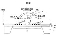
- the temperature distributions 12a and 12b shown in FIG. 2 are temperature distributions on the XX ′ line of the sensor element.
- the temperature distribution 12a is a temperature distribution on the surface of the diaphragm 2 when there is no wind
- the temperature distribution 12b is a temperature distribution on the surface of the diaphragm 2 when an air flow is generated.
- the upstream side of the heating resistor 4 is cooled by the air flow to lower the temperature, and the downstream side passes through the heating resistor 4 and heated air flows to increase the temperature.
- the flow rate can be measured by measuring the temperature difference ⁇ Ts between the upstream portion and the downstream portion of the heating resistor 4 by the upstream side temperature sensitive resistors 6a, 6b and the downstream side temperature sensitive resistors 7a, 7b. .
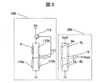
- the circuit shown in FIG. 3 includes a drive circuit 100 that applies a drive voltage Vh necessary to cause the heating resistor 4 to generate heat, and a bridge circuit 200 that measures ⁇ Ts.
- the drive circuit 100 forms a bridge circuit in which a series circuit composed of the heating resistor 4 and the fixed resistor 110a and a series circuit composed of the fixed resistor 110b and the fixed resistor 110c are connected in parallel. Vh is applied. The intermediate voltage of these series circuits is taken out and connected to the amplifier 111. The output of the amplifier 111 is connected to the base of the transistor 112. The collector of the transistor 112 is connected to Vh, and the emitter is connected to the heating resistor 4 to constitute a feedback circuit.
- the fixed resistors 110 a, 110 b, and 110 c are disposed at locations that are thermally isolated from the heating resistor 4. For example, it may be disposed on a portion of the semiconductor substrate 1 that is not on the diaphragm 2, or may be provided on another portion that is not on the semiconductor substrate 1.
- the bridge circuit 200 has a bridge circuit configuration in which a series circuit composed of temperature sensitive resistors 6a and 7a and a series circuit composed of 6b and 7b are connected in parallel, and a reference voltage Vref is applied.
- the resistance value changes according to the temperature of each resistor.
- a change occurs in the resistance balance of the bridge circuit, and a differential voltage is generated between the intermediate voltages.
- An output Vout corresponding to the flow rate is obtained from the difference voltage by the amplifier 13.
- the temperature sensitive resistor is disposed upstream of the heat generating resistor in the fluid flow direction, the upstream temperature sensitive resistors 6a and 6b, and the fluid flow direction with respect to the heat generating resistor.
- the downstream side temperature sensitive resistors 7a and 7b are arranged on the upstream side, and as shown in FIG.
- the upstream side temperature sensitive resistors 6a and 6b and the downstream side temperature sensitive resistors 7a and 7b are longitudinal.
- the configuration is substantially symmetrical with respect to the axis. With such a configuration, it is possible to detect the flow rate of the fluid to be measured in the forward flow direction and the reverse flow direction.
- the length L1 from the short side end of the diaphragm 2 on the side where the wiring portion 5 is disposed to the end of the heating resistor 4, the width Wd of the diaphragm 2 in the XX′-axis direction, and the heating resistance If the trapezoidal region consisting of the width Wh in the XX′-axis direction of the body 4 is defined as region 1 and the trapezoidal region composed of L2, Wd and Wh is defined as region 2, the thermal resistance Rt1 in the YY′-axis direction in region 1 The thermal resistance Rt2 in the YY′-axis direction in the region 2 can be expressed by Equations 1 and 2, respectively.
- Rt1 L1 ⁇ log (Wh / Wd) / ((K1t1 + k2t2 + ⁇ 1k3t3) (Wh ⁇ Wd)) (Formula 1)
- Rt2 L2 ⁇ log (Wh / Wd) / ((K1t1 + k2t2 + ⁇ 2k3t3) (Wh ⁇ Wd))
- k1 and t1 are a heat transfer coefficient and a film thickness of a material (for example, silicon dioxide) constituting the electrical insulating films 3a and 3b.
- K2 and t2 are a heat transfer coefficient and a film thickness of a material (for example, silicon nitride) constituting the electric insulating films 3a and 3b.
- K3 and t3 are the heat conduction coefficient and film thickness of the heating resistor 4, the temperature sensitive resistors 6a, 6b, 7a, 7b and the material constituting the wiring part 5 (for example, polycrystalline silicon doped with impurities). is there.
- ⁇ 1 is the total area of the heating resistor 4, the temperature sensitive resistors 6a, 6b, 7a, 7b and the wiring portion 5 being region 1. It is a ratio to ⁇ 2 is the ratio of the total area of the heating resistor 4, the temperature sensitive resistors 6a, 6b, 7a, 7b and the wiring portion 5 to the region 2.
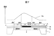
- FIG. 7 shows a cross-sectional structure along the line YY ′ of this sensor element.
- the electric insulating films 3 a and 3 b and the wiring part 5 constitute the region 1
- the electric insulating films 3 a and 3 b constitute the region 2.
- the heating resistor 4, the upstream temperature sensing resistors 6a and 6b, the downstream temperature sensing resistors 7a and 7b, and the wiring portion 5 are made of, for example, a semiconductor such as polycrystalline silicon or single crystal silicon doped with impurities.
- the electrical insulating films 3a and 3b are formed of silicon dioxide or silicon nitride.
- semiconductor materials such as polycrystalline silicon and single crystal silicon doped with impurities and metal materials such as platinum, molybdenum, tungsten, and nickel alloys have lower thermal resistance than silicon dioxide and silicon nitride. Therefore, the relationship between the length L1 in the YY'-axis direction in the region 1 and the thermal resistance Rt1 and the relationship between the length L2 in the YY'-axis direction in the region 2 and the thermal resistance Rt2 are as shown in FIG.
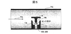
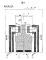
- FIG. 5 shows an example of sensor element mounting.
- a base member 16 having a shape protruding from the wall surface of the passage 14a is provided in the passage 14a through which the air flow 15a flows.
- a sub-passage 14b is formed in the base member 16, and a part of the air flow 15a flowing in the passage 14a is formed. It is a structure that is taken in.
- the base member 16 is provided with a circuit board 17 on which the drive circuit 100 and the detection circuit 200 are mounted, and is arranged so that a part of the circuit board 17 protrudes into the sub passage 14b.
- a sensor element is arrange
- the sub-passage 14b has a structure bent in a substantially U shape. For this reason, in the sub-passage 14b, the inertial force generated in the air flow 15b changes according to the flow rate, so the direction of the air flow 15b on the sensor element changes according to the flow rate.
- the sub passage 14b is bent in a substantially U shape.
- the structure of the sub passage 14b is not limited to this, and inertia force is generated in the air flow 15b taken into the sub passage 14b.
- Such a structure may be used.
- centrifugal force acts on the air flow 15b taken into the sub passage 14b. Accordingly, the direction of the air flow 15b on the sensor element changes according to the flow rate.
- the sensitivity change occurs due to the change in the direction of air flow, which causes a decrease in the flow rate measurement accuracy.
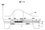
- the heating resistor 4 is arranged at a position satisfying L1> L2, as shown in FIG.
- FIG. 10 shows a cross-sectional structure along the line YY ′ of the sensor element of FIG. 1 and a temperature distribution on the surface of the diaphragm 2.
- Equations 1 and 2 by setting L1> L2, there is an effect of making Rt1 larger and Rt2 smaller. Therefore, as shown in FIG. 11, when L1> L2, Rt1 and Rt2 can be made substantially equal.
- the temperature distribution on the sensor element at this time takes the form of a temperature distribution 18b in FIG.
- FIG. 12 is a diagram showing an isotherm 19b representing the state of the temperature distribution 18b.
- the air flow that has risen in temperature through the heating resistor 4 flows to the downstream temperature sensitive resistors 7a and 7b.
- the temperatures of the places where the air flow 20a and the air flow 20b pass on the heating resistor 4 are substantially the same, the temperature of the air flowing into the downstream temperature sensitive resistors 7a and 7b is the air flow 20a even in the air flow 20a. Even in the case of the flow 20b, the temperature is almost the same.
- the wiring part 5 is preferably provided with a width larger than the line width of the heating resistor 4. Thereby, the resistance value of the wiring part 5 can be reduced, the temperature rise due to the current flowing through the wiring part 5 can be reduced, and the temperature distribution around the heating resistor 4 can be made more uniform.
- the ratio L1 / L2 of L1 and L2 is preferably 1.5 or more.
- ⁇ 2 0.
- the material constituting the heating resistor 4, the temperature sensitive resistors 6a, 6b, 7a, 7b, and the wiring portion 5 is formed with the silicon dioxide film thickness t1 constituting the electrical insulating films 3a and 3b and the silicon nitride film thickness t2.
- the ratio of the heating resistor 4 By sufficiently increasing the film thickness t3, the ratio of the heating resistor 4, the temperature sensitive resistors 6a, 6b, 7a, 7b and the wiring part 5 to the thermal resistances Rt1, Rt2 can be made relatively small. it can.
- silicon nitride has a large tensile stress (1 GPa)
- the film thickness t2 becomes too large, cracks may be generated in the diaphragm, which causes damage to the electrical insulating films 3a and 3b. Therefore, it is necessary to pay attention to internal stress.
- the internal stress sharply increases when L1 / L2 ⁇ 1.5.
- L1 / L2 1.4
- an internal stress of about 1 MPa ⁇ ⁇ m is generated, and the electric insulating films 3a and 3b may be damaged.
- L1 / L2 ⁇ 1.5 the internal stress is stably small.
- the configuration of L1 / L2 ⁇ 1.5 is also effective when the sensor element is downsized.
- FIG. 14 shows the correlation between L1 / L2 and the temperature difference ⁇ Tab between point A and point B when the thickness of the electrical insulating films 3a and 3b is constant.
- the inequality of the thermal resistance in the longitudinal direction of the region 1 and the region 2 can be relaxed, the unevenness of the temperature distribution can be improved, and the electrical insulating film can be made thinner, Further downsizing and higher sensitivity can be achieved.
- Example 2 A second embodiment according to the present invention will be described below with reference to FIGS.
- FIG. 15 is a diagram showing the configuration of the sensor element of the thermal flow meter in the present embodiment.
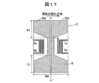
- an adjustment body 21 having a shape symmetrical to the YY ′ axis is provided in the vicinity of the heating resistor 4 in the region 2. It is constituted by.
- the adjusting body 21 is formed using, for example, the same material as the heating resistor 4, and an additional resist pattern is formed when the heating resistor 4 and the temperature sensitive resistors 6 a, 6 b, 7 a, 7 b and the wiring part 5 are molded. It can be formed by providing.
- the adjustment body 21 is configured using the same material as each resistor, whereby the layer structure of the region 2 (for example, silicon dioxide and silicon nitride) is changed to the layer structure of the region 1 (for example, Silicon dioxide and silicon nitride and polycrystalline silicon). Therefore, the values of the thermal resistances Rt1 and Rt2 can be made closer. That is, the unequality of the thermal resistance in the longitudinal direction of the region 1 and the region 2 can be further reduced, and a favorable temperature distribution with no bias can be obtained as shown in 18c.
- the layer structure of the region 2 for example, silicon dioxide and silicon nitride
- the layer structure of the region 1 for example, Silicon dioxide and silicon nitride and polycrystalline silicon
- the adjustment body 21 is provided in the region 2 so that the temperature distribution can be improved without changing the dimensions of the sensor element. It is.
- the shape of the adjusting body 21 may be a polygonal shape as shown in FIG. 15, or may be a divided shape. Further, as means for enhancing the effect, the area ratio ⁇ 2 occupied by the adjusting body 21 in the region 2 may be obtained by Expression 4 and reflected in the structure. Thereby, Rt1 and Rt2 can be made substantially equal, and a higher effect can be obtained.
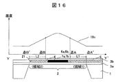
- the diaphragm 2 in the third embodiment is configured by providing pseudo wiring portions 22a and 22b substantially symmetrical to the wiring portion 5 in the region 2 in addition to the configuration of the diaphragm 2 of the sensor element of FIG.
- the pseudo wiring portions 22a and 22b are configured by using the same material as that of the heating resistor 4, for example.
- the pseudo wiring portions 22a and 22b can be formed by providing an additional resist pattern when the heating resistor 4 and the temperature sensitive resistors 6a, 6b, 7a and 7b and the wiring portion 5 are molded. Then, the cross-sectional structure of the sensor element is a region 1 as shown in FIG.
- the thermal resistances Rt1 and Rt2 are substantially equal to those of the equations 1 and 2. Therefore, as shown in the temperature distribution 18d of FIG. 18, the temperature distribution on the sensor element can be a good temperature distribution with no bias. That is, the inequality of the thermal resistance in the longitudinal direction of the region 1 and the region 2 can be alleviated, and the unevenness of the temperature distribution can be improved.
- Example 4 A fourth embodiment according to the present invention will be described below.
- a protective film 23 is formed in the upper layer of the electric insulating film 3b in addition to the electric insulating films 3a and 3b in the region 2. Consists of.
- the protective film 23 is configured by using, for example, the same material as the electrical insulating films 3a and 3b.
- the sectional structure of the sensor element is configured such that the film thickness T2 in the region 2 is thicker than the film thickness T1 in the region 1. Rt2 at this time can be expressed by Equation 5.
- Rt2 L2 ⁇ log (Wh / Wd) / ((K1t1 + k2t2 + ⁇ 2k3t3 + k4t4) (Wh ⁇ Wd)) ...
- k4 is a heat transfer coefficient of the protective film 23.
- T4 is the thickness of the protective film 23.
- Other symbols are the same as those described in the first embodiment. According to Equation 5, by forming the protective film 23, the thermal resistance Rt2 becomes small and approaches the magnitude of Rt1. Further, the value of t4 when Rt1 of Expression 1 is equal to Rt2 of Expression 5 is obtained by Expression 6.
- the film thickness t4 of the protective film 23 can be made closer to the film thickness obtained by Expression 6, so that Rt1 ⁇ Rt2, and the temperature distribution on the sensor element is the temperature distribution 18e in FIG. As shown, a good temperature distribution with no bias can be obtained. That is, the inequality of the thermal resistance in the longitudinal direction of the region 1 and the region 2 can be reduced, and the unevenness of the temperature distribution can be improved.
- Example 5 A fifth embodiment according to the present invention will be described below.
- the sensor element in the fifth embodiment is configured by providing a structure in which an inclination is provided at the film thickness changing point 24 where the film thickness of the diaphragm 2 changes from T1 to T2 in the sensor element of the fourth embodiment. With this configuration, the stress generated at the boundary between the film thickness T1 and the film thickness T2 is dispersed.
- the thermal flow sensor When the thermal flow sensor is mounted on an internal combustion engine of an automobile, the heating resistor 4 generates heat on the surface of the diaphragm 2, and the ambient temperature of the sensor changes greatly. Therefore, mechanical stress such as thermal stress or vibration may lead to the diaphragm 2 being damaged.
- the stress generated at the boundary between the film thicknesses T1 and T2 can be dispersed, the strength and the strength of the diaphragm 2 can be reduced while alleviating the unequal thermal resistance in the longitudinal direction of the regions 1 and 2.
- the durability and strength of the electric insulating film can be improved, and a highly reliable flow sensor can be realized.
- Example 6 A sixth embodiment according to the present invention will be described below.
- the sensor element in the sixth embodiment is protected so that the boundary line 25 formed by the boundary between the film thickness T1 and the film thickness T2 has at least one bent portion in the diaphragm 2 of the fourth embodiment. It is configured by forming the film 23. With this configuration, a mechanical stress is dispersed at the boundary between the film thickness T1 and the film thickness T2. Therefore, the strength and durability of the diaphragm 2 and the strength of the electrical insulating film can be improved while reducing the unequal thermal resistance in the longitudinal direction of the region 1 and the region 2, and a highly reliable flow sensor is realized. can do.
- Example 7 A seventh embodiment according to the present invention will be described below with reference to FIGS.
- the sensor element in the seventh embodiment is provided with a temperature measuring resistor 26 in the vicinity of the heating resistor 4 and further has fixed resistors 27a, 27b, and 27c in the diaphragm 2. Form outside. Subsequently, a bridge circuit is formed by the resistance temperature detector 26 and the fixed resistors 27a, 27b, and 27c, and an intermediate voltage of each resistor is connected to the lead wiring portions 28a, 28b, 28c, and 28d and the electrode pad portion 11.
- the temperature distribution 12a indicates the temperature distribution on the surface of the diaphragm 2 when there is no wind.
- the temperature distribution 12b is a temperature distribution on the surface of the diaphragm 2 when an air flow is generated.
- the upstream side of the heating resistor 4 is cooled by the air flow to lower the temperature, and the downstream side passes through the heating resistor 4 and heated air flows to increase the temperature. Therefore, the flow rate can be measured by measuring the temperature difference ⁇ Ts between the upstream side and the downstream side of the heating resistor 4 by the upstream side temperature sensitive resistors 6a, 6b and the downstream side temperature sensitive resistors 7a, 7b.
- the drive circuit 101 in the seventh embodiment includes a series circuit composed of a temperature measuring resistor 26 and a fixed resistor 27a whose resistance value varies depending on the temperature of the heating resistor 4, and a series composed of a fixed resistor 27b and a fixed resistor 27c.
- a bridge circuit is formed by connecting the circuits in parallel, and a reference voltage Vref is applied to each series circuit. The intermediate voltage of these series circuits is taken out and connected to the amplifier 29. The output of the amplifier 29 is connected to the base of the transistor 30.
- the collector of the transistor 30 is connected to the power source Vh, and the emitter is connected to the heating resistor 4 to constitute a feedback circuit.
- the detection circuit in the seventh embodiment has the same configuration as that of the bridge circuit 200 in the first embodiment.
- the bridge circuit 200 has a bridge circuit configuration in which a series circuit composed of temperature sensitive resistors 6a and 7a and a series circuit composed of 6b and 7b are connected in parallel, and a reference voltage Vref is applied.
- a temperature difference ⁇ Ts occurs between the upstream temperature sensing resistors 6a, 6b and the downstream temperature sensing resistors 7a, 7b due to the air flow
- the upstream temperature sensing resistors 6a, 6b and the downstream temperature sensing resistors Since the resistance values of 7a and 7b change according to the respective temperatures, the resistance balance of the bridge circuit changes, and a differential voltage is generated between the intermediate voltages.
- An output Vout corresponding to the flow rate is obtained from the difference voltage by the amplifier 13.
- the advantage obtained by the thermal flow sensor of the seventh embodiment is that, in addition to the advantage obtained by the thermal flow sensor of the first embodiment, the power supplied to the heating resistor 4 can be reduced, and the heating resistor The body 4 can be further reduced in size. Accordingly, the degree of freedom of arrangement of the heating resistor 4 in the diaphragm 2 is improved, and the heating resistor 4 can be arranged at a location that is more advantageous for improving the temperature distribution.
- This embodiment can also be applied to the second to sixth embodiments and the eighth embodiment described later.
- Example 8 The eighth embodiment according to the present invention will be described below.
- the heating resistor 4 in the eighth embodiment has a configuration in which the wiring width is narrower than that of the heating resistor 4 in the first embodiment and a number of folded shapes are provided. Thereby, the heat generation density per unit area can be improved.
- the heating temperature of the thermal resistor 4 can be increased. Since power consumption increases, in order to perform sensor operation with low power consumption, low voltage, and low current, it is desirable to make the heating resistor 4 smaller.
- the advantage of the eighth embodiment is that, in addition to the advantage obtained by the thermal flow sensor in the first embodiment, the heat generation density per unit area of the heat generating resistor 4 is increased, so that the heat generation amount can be increased and at the same time the heat generation resistance.
- the body 4 can be miniaturized. Accordingly, the degree of freedom of arrangement of the heating resistor 4 in the diaphragm 2 is improved, and it becomes possible to arrange the heating resistor 4 in a portion that is more advantageous for improving the temperature distribution.
- This embodiment can also be applied to the second to seventh embodiments.
- heating resistor 4 in the present embodiment is substantially M-shaped, the same effect can be obtained in a substantially U-shaped or meandered (meandering) shape.
- Base member 17 ... Circuit boards 19a and 19b ... Isothermal lines 20a and 20b ... Air flow direction 21 ... Adjustment bodies 22a and 22b ... Pseudo wiring part 23 ... Protective film 24 ... Film thickness change point 25 ... Film thickness Boundary line 26 ... Resistance temperature detectors 27a, 27b, 27c, 110a, 110b, 110c ... Fixed resistors 30, 112 Transistors 100 and 101 ... drive circuit 111 ... operational amplifier 200 ... All publications cited in the detection circuit herein shall incorporate herein patents and patent applications as reference.
Abstract
本発明の目的は、空気流の流れ方向の変化によるセンサ素子の検出感度の変化を低減し、小型・高精度な熱式流量センサを提供することにある。 本発明の実施形態は、半導体基板1上に形成した空洞部2と、前記空洞部2を覆うように形成した電気絶縁膜と、前記電気絶縁膜上に形成した発熱抵抗体4と、前記発熱抵抗体の近傍に形成した感温抵抗体と、前記半導体基板の周縁部において周縁に対して略並行に配置した導電体からなる電極部11と、前記電極部と前記発熱抵抗体とを電気的に接続する配線部5とを有し、被計測流体と前記感温抵抗体との伝熱量に基づいて被計測流体の流量を検出する熱式流量センサにおいて、前記発熱抵抗体の前記電極部側の一辺と前記空洞部の前記電極部側の一辺とからなる第1領域の熱抵抗と、前記発熱抵抗体の一辺と対向する他辺と前記空洞部の一辺と対向する他辺とからなる第2領域の熱抵抗とがほぼ等しくなるように熱抵抗を調整する。
Description
本発明は、被計測流体中に発熱抵抗体を設置し流量を測定する熱式流量センサに係り、特に、自動車の内燃機関の吸入空気流量や排ガス流量の測定に好適な熱式流量センサに関する。
自動車などの内燃機関の吸入空気量を検出する空気流量センサとして、質量流量を直接測定できる熱式の空気流量センサが主流になっている。
近年では、マイクロマシン技術を用いてシリコン(Si)などの半導体基板上に熱式流量計のセンサ素子を製造するものが提案されている。このような半導体タイプのセンサ素子は、半導体基板の一部を矩形状に除去した空洞部を形成し、この空洞部に形成した数ミクロン厚の電気絶縁膜上に発熱抵抗体を形成している。また、このようなセンサ素子では、発熱抵抗体の近傍に感温抵抗体を形成し、発熱抵抗体上を流れる被計測流体から感温抵抗体への伝熱量をもとに流量を測定する方法が主流となっている。発熱抵抗体の大きさは数百ミクロンと微細であり、数ミクロンの薄膜状に形成されることから、熱容量が小さく高速応答・低消費電力化が可能である。
その反面、流路上に存在するオイルやダストなどの飛散物による破損など信頼性においては現在も様々な改善取り組みがなされている。例えば、センサ素子の汚損を低減するために、空気流の一部を取り込む通路内にセンサ素子を配置し、この通路を多様な形状に曲げることにより慣性効果を用いてオイルやダストなどがセンサ素子に衝突しにくい構造をとる方法がある。
しかし、このような多様な形状で曲げた構造の通路にセンサ素子を配置したとき、通路内を流れる流量に応じて空気流に働く慣性効果が変化し、センサ素子上を流れる空気の方向が流量に応じて変化してしまう。そして、センサ素子上を流れる空気の方向が変化すると、センサ素子で検出した流量に誤差が発生してしまう。
この原因の一因としては、発熱抵抗体周辺の構造の不均一性に伴い発熱抵抗体周辺の温度分布が不均一となるため、空気流量方向の微小な変化でもセンサ素子の検出感度が変化するという点がある。さらに、発熱抵抗体が小型になると、発熱抵抗体の周辺の温度分布の均一性がさらに悪化して測定誤差がさらに大きくなる。この問題を解決するために、例えば、特許文献1では、発熱抵抗体の配線幅を局所的に増減させることによって発熱抵抗体の発熱量を調節し、温度分布の平滑化を図っている。
しかし、従来では、発熱抵抗体の配線幅が局所的に相対的に細くなる部分があり、また小型のセンサ素子を構成する際に該当部位の強度が低下するため、オイルやダスト等による破損や、エレクトロマイグレーション等による劣化の恐れがある。特許文献1では発熱抵抗体周辺の温度分布に関しては考慮されていたが、発熱抵抗体の構造強度に関しては十分な配慮がなされていなかった。
そこで、本発明は上記課題に鑑みてされたものであり、その目的とするところは、自動車などの内燃機関に搭載する際に、発熱抵抗体の構造強度を低下することなく、空気流の流れ方向の微小な変化によるセンサ素子の検出感度の変化を低減することで流量測定誤差を低減し、小型かつ低消費電力で高精度な熱式流量センサを提供することにある。
上記目的を達成するために、本発明の熱式流量センサは、発熱抵抗体の電極部側の一辺と前ダイアフラム部の電極部側の一辺とからなる第1領域の熱抵抗と、発熱抵抗体の一辺と対向する他辺と空洞部の一辺と対向する他辺とからなる第2領域の熱抵抗とがほぼ等しくなるように熱抵抗を調整する構成とした。
本明細書は本願の優先権の基礎である日本国特許出願2010-220248号の明細書および/または図面に記載される内容を包含する。
本発明によれば、空気流の流れ方向の微小な変化によるセンサ素子の検出感度の変化を低減することで流量測定誤差を低減し、小型かつ低消費電力で高精度な熱式流量センサを提供することができる。
以下、本発明に係る一実施例について図1から図26を用いて説明する。
実施例1
本発明に係る第1の実施例について、以下説明する。
本発明に係る第1の実施例について、以下説明する。
本実施例による熱式流量計のセンサ素子の構成について、図1,図2を用いて説明する。
図1において、センサ素子を構成する半導体基板1は、ケイ素(Si)やセラミック等の熱伝導率の良い材料で構成される。そして、半導体基板1上に電気絶縁膜3aを形成し、半導体基板1を裏面からエッチングすることで空洞部を形成しダイアフラム2を形成する。ダイアフラム2上の電気絶縁膜3aの表面には発熱抵抗体4と発熱抵抗体4に通電するための配線部5とを形成する。
ここで、発熱抵抗体4は、Y-Y′線方向に対して、配線部5が形成される側の空洞部2の短辺の端部から発熱抵抗体4の配線部側端部までの距離をL1、配線部5が形成される側とは反対側の空洞部2の短辺の端部から発熱抵抗体4の先端部までの距離をL2とすると、L1>L2なる位置に発熱抵抗体4を配置する。また、X-X′線方向に対しては、ダイアフラム2の中央に発熱抵抗体4を配置する。
さらに、発熱抵抗体4の両側には上流側感温抵抗体6a,6b,下流側感温抵抗体7a,7bを形成する。上流側感温抵抗体6a,6bは発熱抵抗体4に対して流体の流れ方向の上流側に配置し、下流側感温抵抗体7a,7bは発熱抵抗体4に対して流体の流れ方向の下流側に配置する。さらに、センサ素子の最表面は電気絶縁膜3bによって覆われ、電気絶縁膜3bは電気的絶縁を行うほか保護膜として働く。さらに、ダイアフラム2外部の半導体基板1上には、発熱抵抗体4,上流側感温抵抗体6a,6b,下流側感温抵抗体7
a,7bを構成する各抵抗体を駆動・検出回路と接続するための引出し配線部8,9,10及び電極パッド部11を設ける。尚、電極パッド部11はアルミニウム(Al)などで形成する。
a,7bを構成する各抵抗体を駆動・検出回路と接続するための引出し配線部8,9,10及び電極パッド部11を設ける。尚、電極パッド部11はアルミニウム(Al)などで形成する。
ここで、これらの発熱抵抗体4,上流側感温抵抗体6a,6b,下流側感温抵抗体7a,7bは温度によって抵抗値が変化する比較的抵抗温度係数が大きい材料で形成する。例えば、不純物をドープした多結晶ケイ素や単結晶ケイ素などの半導体材料、また白金(Pt),モリブデン(Mo),タングステン(W),ニッケル合金などの金属材料などで形成すると良い。また、電気絶縁膜3a,3bは二酸化ケイ素(SiO2)や窒化ケイ素(Si3N4)により約2ミクロン厚の薄膜状に形成し、熱絶縁効果が十分に得られる構造とする。
また、発熱抵抗体4はダイアフラム2上の発熱の主となる部分であり、発熱抵抗体4に電気的に接続されていたとしても、配線部5の様に配線幅を広くすることにより単位長さあたりの抵抗値を小さくしている部位や、発熱抵抗体4からの突起状に形成されたパターン等の電流通路として成り立たない部位は発熱抵抗体4の範囲には含まれない。例えば、発熱抵抗体4の単位長さあたりの抵抗値は、配線部5の単位長さあたりの抵抗値に対して10倍以上大きいことが望ましい。
次に、第1実施例のセンサ素子の製造方法に関して説明する。
半導体基板1としては、単結晶ケイ素等の半導体を用いる。ベースとなる単結晶ケイ素による半導体基板1の表面を、熱酸化あるいはCVD法等により所定の厚さ約1μmの電気絶縁膜3aとなる二酸化ケイ素と窒化ケイ素を形成する。次に、抵抗体として、厚さ約1μmの多結晶ケイ素半導体薄膜をCVD法等により積層する。
次に、多結晶ケイ素半導体薄膜に不純物拡散を行い、所定の抵抗率となるように高濃度ドープ処理を行う。更に、ホトリソグラフィ技術によりレジストを所定の形状に形成した後、反応性イオンエッチング等の方法により多結晶ケイ素半導体薄膜をパターニングし、発熱抵抗体4,配線部5,感温抵抗体6a,6b,7a,7b,引出し配線部8a,8b,9a~9d,10a~10dが得られる。
その後、工程では保護膜として電気絶縁膜3bを電気絶縁膜3aと同様に、二酸化ケイ素と窒化ケイ素を約1ミクロン厚にCVD法等により形成する。
次に、外部回路との接続のための端子となる端子電極が電極パッド部11に保護膜3bを除去し、アルミニウム,金等で形成される。なお、各抵抗体と端子を接続するための引出し配線部8a,8b,9a~9d,10a~10dを、多結晶ケイ素半導体薄膜とアルミニウム,金等の多層膜構成としてもかまわない。
最終工程では、単結晶ケイ素半導体基板1の裏面にエッチングのマスク材を所定の形状にパターニングし、水酸化カリウム(KOH)等のエッチング液を用いて異方性エッチングすることにより空洞部を形成して、ダイアフラム2を形成する。
以上の工程により、センサ素子が完成する。
次に、熱式流量センサの検出原理について図2を用いて説明する。
図2に示した温度分布12a,12bはセンサ素子のX-X′線上の温度分布である。温度分布12aは、無風時のダイアフラム2表面上の温度分布であり、温度分布12bは、空気流が発生したときのダイアフラム2表面上の温度分布である。空気流が発生することにより、発熱抵抗体4の上流側は空気流により冷却され温度が下がり、下流側は発熱抵抗体4を通過し加熱された空気が流れることから温度が上がる。したがって、上流側感温抵抗体6a,6bと下流側感温抵抗体7a,7bとによって発熱抵抗体4の上流部と下流部の温度差ΔTsを測定することにより、流量を計測することができる。
次に、温度差ΔTsを測定するための回路動作について図3を用いて解説する。
図3に示す回路は、発熱抵抗体4を発熱させるために必要な駆動電圧Vhを印加する駆動回路100と、ΔTsを測定するためのブリッジ回路200により構成する。駆動回路100は、発熱抵抗体4と固定抵抗110aとからなる直列回路と、固定抵抗110bと固定抵抗110cとからなる直列回路とを並列に接続したブリッジ回路を構成し、各直列回路に駆動電圧Vhを印加する。これらの直列回路の中間電圧を取り出し、増幅器111に接続する。増幅器111の出力は、トランジスタ112のベースに接続する。トランジスタ112のコレクタをVhに接続し、エミッタは発熱抵抗体4に接続し、フィードバック回路を構成する。これにより、発熱抵抗体4の温度Thは空気流の温度Taに対して一定温度ΔT(=Th-Ta)高くなるように制御される。尚、固定抵抗110a、110b、110cは、発熱抵抗体4に対して熱的に隔離された場所に配置する。例えば、半導体基板1上であってダイアフラム2上でない部分に配置してもよく、また半導体基板1上でない別の部位に設けても良い。ブリッジ回路200は、感温抵抗体6a及び7aからなる直列回路と、6b及び7bからなる直列回路とを並列に接続したブリッジ回路構成をとり、基準電圧Vrefが印加される。次に、空気流により上流側感温抵抗体6a,6bと下流側感温抵抗体7a,7bとに温度差ΔTsが発生すると、各抵抗体それぞれの温度に応じて抵抗値が変化するため、ブリッジ回路の抵抗バランスに変化が生じ、各中間電圧間には差電圧が発生する。この差電圧から増幅器13によって流量に応じた出力Voutが得られる。なお、上述したように、感温抵抗体は発熱抵抗体に対して流体の流れ方向の上流側に配置された上流側感温抵抗体6a,6bと、発熱抵抗体に対して流体の流れ方向の上流側に配置された下流側感温抵抗体7a,7bを有し、さらに、図1に示すように、上流側感温抵抗体6a,6bおよび下流側感温抵抗体7a,7bは長手軸に対して略対称に構成する。このような構成にすることで、被計測流体の順流方向および逆流方向の流量を検出することができる。
次に、第1実施例により得られる効果について、図4~図12を用いて説明する。
図4において、配線部5が配置される側のダイアフラム2の短辺端部から、発熱抵抗体4の端部までの長さL1とダイアフラム2のX-X′軸方向の幅Wdおよび発熱抵抗体4のX-X′軸方向の幅Whからなる台形領域を領域1とし、L2とWdおよびWhからなる台形領域を領域2とすると、領域1におけるY-Y′軸方向への熱抵抗Rt1および領域2におけるY-Y′軸方向への熱抵抗Rt2は、それぞれ式1,式2により表すことができる。
Rt1=L1×log(Wh/Wd)
/((k1t1+k2t2+η1k3t3)(Wh-Wd)) …(式1)
Rt2=L2×log(Wh/Wd)
/((k1t1+k2t2+η2k3t3)(Wh-Wd)) …(式2)
ここで、k1,t1は電気絶縁膜3a,3bを構成する素材(例えば、二酸化ケイ素など)の熱伝達係数および膜厚である。また、k2,t2は電気絶縁膜3a,3bを構成する素材(例えば、窒化ケイ素など)の熱伝達係数および膜厚である。また、k3,t3は発熱抵抗体4,感温抵抗体6a,6b,7a,7bおよび配線部5を構成する素材(例えば、不純物をドープした多結晶ケイ素など)の熱伝導係数および膜厚である。また、η1は発熱抵抗体4,感温抵抗体6a,6b,7a,7bおよび配線部5の合計面積が領域1
に占める比率である。また、η2は発熱抵抗体4,感温抵抗体6a,6b,7a,7bおよび配線部5の合計面積が領域2に占める比率である。
図6のセンサ素子は、発熱抵抗体4のY-Y′軸方向の配置がL1=L2となる様に配置されている。このセンサ素子のY-Y′線に沿った断面構造を図7に示す。センサ素子は、電気絶縁膜3a,3b及び配線部5が領域1を構成しており、電気絶縁膜3a,3bが領域2を構成する。ここで、発熱抵抗体4,上流側感温抵抗体6a,6b,下流側感温抵抗体7a,7b、及び配線部5は、例えば、不純物をドープした多結晶ケイ素や単結晶ケイ素などの半導体材料、また白金,モリブデン,タングステン,ニッケル合金などの金属材料などで形成する。また、電気絶縁膜3a,3bは二酸化ケイ素や窒化ケイ素により形成する。一般的に、不純物をドープした多結晶シリコンや単結晶シリコンなどの半導体材料や、白金,モリブデン,タングステン,ニッケル合金などの金属材料は、二酸化ケイ素や窒化ケイ素に比べて熱抵抗が小さい。故に、領域1におけるY-Y′軸方向の長さL1と熱抵抗Rt1の関係と領域2におけるY-Y′軸方向の長さL2と熱抵抗Rt2の関係は図8に示す様に、領域1の方が1/Lの増加に応じた熱抵抗の増加率が小さい。そのため、L1=L2の場合は、センサ素子上の温度は点Aよりも点B側が高い状態となり、
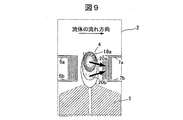
Y-Y′軸方向の温度分布は図7のような温度分布18aの形をとる。また、このときのセンサ素子の平面図における温度分布18aの状態を表す等温線19aは図9で示される通りである。
Y-Y′軸方向の温度分布は図7のような温度分布18aの形をとる。また、このときのセンサ素子の平面図における温度分布18aの状態を表す等温線19aは図9で示される通りである。
ここで、センサ素子の実装形態例を図5に示す。空気流15aが流れる通路14a内に、通路14aの壁面から突出する形状のベース部材16を設け、ベース部材16にはサブ通路14bが形成されており、通路14a内を流れる空気流15aの一部が取り込まれる構造となっている。また、ベース部材16には駆動回路100および検出回路200を搭載した回路基板17が設けられており、回路基板17の一部がサブ通路14b内に突出する様に配置する。そして、サブ通路14b内に突出した回路基板17上にセンサ素子を配置し、サブ通路14b内を流れる空気流15bにより流量測定を行う。
センサ素子の汚損を低減するために、サブ通路14bは略U字状に曲げた構造としている。そのためサブ通路14bでは、流量に応じて空気流15bに生じる慣性力が変化するため、センサ素子上での空気流15bの方向は流量に応じて変化する。
なお、本実施例ではサブ通路14bの形状を略U字状に曲げた構造としているが、サブ通路14bの構造はこれに限らず、サブ通路14bに取り込まれた空気流15bに慣性力が生じるような構造であればよい。また、慣性力に限らず、センサ素子の汚損を低減するために、サブ通路14bに取り込まれた空気流15bに遠心力が働く構造とする場合もあり、このような場合であっても、流量に応じて遠心力が変化するため、センサ素子上での空気流15bの方向は流量に応じて変化する。
次に、空気流15bの方向が変化することによる検出感度の低下について詳細に説明する。図9の等温線19aの状態において、慣性効果により傾いた空気流20a,20bが、それぞれダイアフラム2に流れ込んだ場合、発熱抵抗体4を通過して温度上昇した空気流が下流側感温抵抗体7a,7bに流れる。発熱抵抗体4上において、空気流20aと空気流20bとで通過する場所の温度が異なるため、下流側感温抵抗体7a,7bに流れ込む空気の温度は、空気流20aの場合、温度が高くなり、空気流20bの場合、温度が低くなる。すると、空気流20aの場合は、より多くの熱量が下流側感温抵抗体7a,7b
に伝わるため、下流側感温抵抗体7a,7bの抵抗値が大きく変化し、良好な検出感度が得られる。一方、空気流20bの場合は、20aの場合に比べて下流側感温抵抗体7a,7bに伝わる熱量が小さいため、下流側感温抵抗体7a,7bの抵抗値の変化は小さく、よって検出感度が低下する。
に伝わるため、下流側感温抵抗体7a,7bの抵抗値が大きく変化し、良好な検出感度が得られる。一方、空気流20bの場合は、20aの場合に比べて下流側感温抵抗体7a,7bに伝わる熱量が小さいため、下流側感温抵抗体7a,7bの抵抗値の変化は小さく、よって検出感度が低下する。
したがって、従来の熱式流量センサでは、空気流の方向が変化することによって感度変化が発生してしまうため、流量測定精度の低下を招いていた。
次に、本発明における第1実施例では、図1に示す様にL1>L2を満たす位置に発熱抵抗体4を配置している。尚、図10は図1のセンサ素子のY-Y′線に沿った断面構造とダイアフラム2表面における温度分布を示す。式1,式2によれば、L1>L2とすることにより、Rt1をより大きく、Rt2をより小さくする効果がある。そのため、図11に示す様に、L1>L2の場合はRt1及びRt2をほぼ同等値とすることができる。この時のセンサ素子上の温度分布は図10の温度分布18bの形をとる。
図12は、温度分布18bの状態を表す等温線19bを示した図である。図12の温度分布19bの状態において、傾いた空気流20a,20bがダイアフラム2に流れ込んだ場合、発熱抵抗体4を通過して温度上昇した空気流が下流側感温抵抗体7a,7bに流れる。発熱抵抗体4上において、空気流20aと空気流20bとで通過する場所の温度はほぼ同じなので、下流側感温抵抗体7a,7bに流れ込む空気の温度は、空気流20aの場合でも、空気流20bの場合でもほぼ同じ温度となる。そのため、空気流の方向が変化しても空気流から下流側感温抵抗体7a,7bに伝わる熱量は変化せず、流量検出において安定した感度を維持することができ、良好に空気流の測定が可能となる。
また、加えて、配線部5は、発熱抵抗体4の線幅よりも大きい幅をもって設けると良い。これにより、配線部5の抵抗値を低減でき、配線部5に流れる電流による温度上昇を低減することができ、発熱抵抗体4周辺の温度分布をより均一にすることができる。
次に、さらに好ましいL1及びL2のとり方を、図13,図14を用いて解説する。
より有益な熱式流量センサを構成するためには、L1及びL2の比率L1/L2が1.5以上となる構造にすると良い。ここで、Rt1=Rt2を満たす時のL1/L2は式3
により算出することができる。ここでは簡単化のため、η2=0としている。
により算出することができる。ここでは簡単化のため、η2=0としている。
L1/L2=(k1t1+k2t2+η1k3t3)/(k1t1+k2t2)
…(式3)
式3によれば、Rt1=Rt2とするためには、L1,L2の比率を変更する方法のほかに、t1,t2≫t3とする方法がある。電気絶縁膜3a,3bを構成する二酸化ケイ素の膜厚t1、および窒化ケイ素の≫膜厚t2を、発熱抵抗体4,感温抵抗体6a,6b,7a,7bおよび配線部5を構成する素材の膜厚t3に対して十分大きくすることにより、発熱抵抗体4,感温抵抗体6a,6b,7a,7bおよび配線部5が熱抵抗Rt1,Rt2に占める割合を相対的に小さくすることができる。しかし、一方で、窒化ケイ素は大きな引張応力(1GPa)を有しているため、膜厚t2が大きくなりすぎると、ダイアフラムにクラックが発生するなど、電気絶縁膜3a,3bの破損要因となることがあるため、内部応力に対して注意を払う必要がある。
図13は、L1/L2とL1/L2においてRt1=Rt2を満足する電気絶縁膜3a,3bの膜厚に応じた内部応力との関係を示す。図13によれば、L1/L2<1.5においては、急峻に内部応力が増加することがわかる。例えば、L1/L2=1.4においては、およそ1MPa・μmの内部応力が生じ、電気絶縁膜3a,3bが破損する可能性がある。一方、L1/L2≧1.5では、内部応力は安定して小さい値となる。
また、L1/L2<1.5の領域においては、Rt1=Rt2を満足するために必要な電気絶縁膜厚が急峻に増大する。対して、より良好な空気流の測定感度を得るためには、電気絶縁膜3a,3bの熱絶縁性を向上させることが必要である。そのため、L1/L2≧1.5の構成とすることは、センサ素子の小型化に際しても有効である。
また、電気絶縁膜3a,3bの膜厚が一定の時のL1/L2と点A―点B間の温度差ΔTabとの相関を図14に示す。図14によれば、L1/L2とΔTabの相関曲線は下降型の収束曲線を描く。さらに検討によれば、L1/L2≧1.5とすれば、L1=L2の場合に対してΔTabを半減以下にすることができる。
これにより、領域1および領域2の長手方向の熱抵抗の不等性を緩和することができ、温度分布の偏りを改善することができ、さらに、電気絶縁膜をより薄膜化することができ、更なる小型化・高感度化を図ることができる。
実施例2
本発明に係る第2の実施例について、図15,図16を用いて以下説明する。
本発明に係る第2の実施例について、図15,図16を用いて以下説明する。
図15は、本実施例における熱式流量計のセンサ素子の構成を示した図である。
第2の実施例におけるセンサ素子は、第1の実施例におけるセンサ素子の構成に加えて、領域2内の発熱抵抗体4近傍に、Y-Y′軸に対称な形状の調整体21を設けることにより構成される。この調整体21は、例えば発熱抵抗体4と同じ素材を用いて形成され、発熱抵抗体4及び感温抵抗体6a,6b,7a,7b、及び配線部5の成型時に、追加のレジストパターンを設けることにより形成することができる。
図16に示す様に、調整体21を、各抵抗体と同じ素材を用いて構成することにより、領域2の層構造(例えば、二酸化ケイ素および窒化ケイ素)を、領域1の層構造(例えば、二酸化ケイ素および窒化ケイ素および多結晶ケイ素)に近づけることができる。故に、熱抵抗Rt1,Rt2の値をより近づけることができる。すなわち、より領域1および領域2の長手方向の熱抵抗の不等性を緩和することができ、18cに示すように偏りのない良好な温度分布にすることができる。
また、小型のセンサ素子においては、センサ素子端部に外部回路と接続するための電極やボンディングワイヤー等の凹凸物が存在するため、凹凸物により発生した乱流が発熱抵抗体4周辺の温度分布に影響を与える可能性がある。そのため、センサ素子の物理寸法が制限され、L1/L2の値が制限される場合がある。本実施例によれば、調整体21を領域2に設けることでセンサ素子の寸法を変更せずに温度分布の偏りを改善することができるため、小型のセンサ素子などに対しては特に効果的である。
また、調整体21の形状は図15に示す様な多角形の形状でもよいが、分割した形状をとっても良い。また、より効果を高める手段として、調整体21が領域2内に占める面積比率η2を式4により求め構造に反映すると良い。これにより、Rt1とRt2をほぼ同等とすることができ、より高い効果が得られる。
η2=(L2/L1)(k1t1+k2t2+η1k3t3)/(k3t3)
…(式4)
実施例3
次に、本発明に係る第3の実施例について、以下説明する。
…(式4)
実施例3
次に、本発明に係る第3の実施例について、以下説明する。
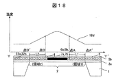
本実施例による熱式流量計のセンサ素子の構成について、図17,図18を用いて説明する。
第3の実施例におけるダイアフラム2は、図4のセンサ素子のダイアフラム2の構成に加えて、領域2内に配線部5と略対称な疑似配線部22a,22bを設けることにより構成する。疑似配線部22a,22bは、例えば発熱抵抗体4と同じ素材を用いて設けることにより構成する。この疑似配線部22a,22bは、発熱抵抗体4及び感温抵抗体6a,6b,7a,7b、及び配線部5の成型時に、追加のレジストパターンを設けることにより形成することができる。すると、センサ素子の断面構造は、図18に示す様に領域1
および領域2の構造が略対称となるため、熱抵抗Rt1およびRt2は、式1及び式2よりほぼ等しくなる。そのため、センサ素子上の温度分布は図18の温度分布18dに示すように、偏りのない良好な温度分布が得られる。すなわち、より領域1および領域2の長手方向の熱抵抗の不等性を緩和することができ、温度分布の偏りを改善することができる。
および領域2の構造が略対称となるため、熱抵抗Rt1およびRt2は、式1及び式2よりほぼ等しくなる。そのため、センサ素子上の温度分布は図18の温度分布18dに示すように、偏りのない良好な温度分布が得られる。すなわち、より領域1および領域2の長手方向の熱抵抗の不等性を緩和することができ、温度分布の偏りを改善することができる。
実施例4
本発明に係る第4の実施例について、以下説明する。
本発明に係る第4の実施例について、以下説明する。
本実施例による熱式流量計のセンサ素子の構成について、図19,図20を用いて解説する。
第4の実施例におけるダイアフラム2は、図4のセンサ素子のダイアフラム2の構成に加えて、領域2において電気絶縁膜3a,3bに加え、電気絶縁膜3bの上層に保護膜23を形成することで構成する。保護膜23は、例えば電気絶縁膜3a,3bと同じ素材を用いて設けることにより構成する。また、図12に示す様に、センサ素子の断面構造は領域1における膜厚T1よりも領域2における膜厚T2の方が厚くなる様に構成する。この
時のRt2は式5により表すことができる。
時のRt2は式5により表すことができる。
Rt2=L2×log(Wh/Wd)
/((k1t1+k2t2+η2k3t3+k4t4)(Wh-Wd))
…(式5)
ここで、k4は保護膜23の熱伝達係数である。またt4は保護膜23の膜厚である。その他の記号については実施例1で説明したものと同様である。式5によれば、保護膜23を形成することにより熱抵抗Rt2は小さくなり、Rt1の大きさに近づく。また、式1のRt1と上記式5のRt2が等しいときのt4の値は、式6により得られる。
/((k1t1+k2t2+η2k3t3+k4t4)(Wh-Wd))
…(式5)
ここで、k4は保護膜23の熱伝達係数である。またt4は保護膜23の膜厚である。その他の記号については実施例1で説明したものと同様である。式5によれば、保護膜23を形成することにより熱抵抗Rt2は小さくなり、Rt1の大きさに近づく。また、式1のRt1と上記式5のRt2が等しいときのt4の値は、式6により得られる。
t4=(L2/L1)(k1t1+k2t2+η1k3t3)
/k4-(k1t1+k2t2+η2k3t3)/k4 …(式6)
式6によれば、保護膜23の膜厚t4を、式6により得た膜厚に近づけることにより、Rt1≒Rt2とすることができ、センサ素子上の温度分布は図20の温度分布18eに示すように、偏りのない良好な温度分布を得られる。すなわち、領域1および領域2の長手方向の熱抵抗の不等性を緩和することができ、温度分布の偏りを改善することができる。
/k4-(k1t1+k2t2+η2k3t3)/k4 …(式6)
式6によれば、保護膜23の膜厚t4を、式6により得た膜厚に近づけることにより、Rt1≒Rt2とすることができ、センサ素子上の温度分布は図20の温度分布18eに示すように、偏りのない良好な温度分布を得られる。すなわち、領域1および領域2の長手方向の熱抵抗の不等性を緩和することができ、温度分布の偏りを改善することができる。
実施例5
本発明に係る第5の実施例について、以下説明する。
本発明に係る第5の実施例について、以下説明する。
本実施例による熱式流量計のセンサ素子の構成について、図21を用いて解説する。
第5の実施例におけるセンサ素子は、第4の実施例のセンサ素子において、ダイアフラム2の膜厚がT1からT2に変化する膜厚変化点24に傾斜を設けた構造をとることにより構成する。本構成とすることにより、膜厚T1と膜厚T2との境界において発生する応力を分散させる構造となる。
熱式流量センサを自動車の内燃機関に搭載した場合、発熱抵抗体4によりダイアフラム2表面上が発熱することに加え、センサの周囲温度が大きく変化する。そのため、熱応力や振動などの機械的応力がダイアフラム2の破損につながる可能性がある。本実施例によれば、膜厚T1及びT2の境界に生じる応力を分散させることができるため、領域1および領域2の長手方向の熱抵抗の不等性を緩和しつつ、ダイアフラム2の強度・耐久性および電気絶縁膜の強度を向上させることができ、高信頼な流量センサを実現することができる。
実施例6
本発明に係る第6の実施例について、以下説明する。
本発明に係る第6の実施例について、以下説明する。
本実施例による熱式流量計のセンサ素子の構成について、図22を用いて解説する。
第6の実施例におけるセンサ素子は、第4の実施例のダイアフラム2内において、膜厚T1と膜厚T2との境界が成す境界線25が、少なくとも1つ以上の屈曲部を有する様に保護膜23を形成することにより構成する。本構成とすることにより、膜厚T1と膜厚T2との境界において、力学的応力を分散させる構造となる。そのため、領域1および領域2の長手方向の熱抵抗の不等性を緩和しつつ、よりダイアフラム2の強度・耐久性および電気絶縁膜の強度を向上させることができ、高信頼な流量センサを実現することができる。
実施例7
本発明に係る第7の実施例について、以下図23~図25を用いて説明する。
本発明に係る第7の実施例について、以下図23~図25を用いて説明する。
本実施例による熱式流量計のセンサ素子の構成について図23を用いて解説する。
第7の実施例におけるセンサ素子は、第1の実施例におけるセンサ素子の構成に加えて、測温抵抗体26を発熱抵抗体4の近傍に設け、さらに固定抵抗27a,27b,27cをダイアフラム2外部に形成する。続いて、測温抵抗体26および固定抵抗27a,27b,27cによりブリッジ回路を形成し、各抵抗体の中間電圧は引出配線部28a,28b,28c,28dおよび電極パッド部11に接続される。
次に、第7の実施例における熱式流量センサの動作原理について、図24を用いて解説する。
図24に示したセンサ素子の断面構成図と共に示した温度分布12a,12bはセンサ素子の表面温度の分布である。温度分布12aは、無風時のダイアフラム2表面上の温度分布を示す。温度分布12bは、空気流が発生したときのダイアフラム2表面上の温度分布である。空気流が発生することにより、発熱抵抗体4の上流側は空気流により冷却され温度が下がり、下流側は発熱抵抗体4を通過し加熱された空気が流れることから温度が上がる。したがって、上流側感温抵抗体6a,6bと下流側感温抵抗体7a,7bとによって発熱抵抗体4の上下流の温度差ΔTsを測定することにより、流量を計測することができる。
次に、第7の実施例における駆動・検出回路について図25を用いて解説する。
第7の実施例における駆動回路101は、発熱抵抗体4の温度によって抵抗値が変化する測温抵抗体26と固定抵抗27aとからなる直列回路と、固定抵抗27bと固定抵抗27cとからなる直列回路とを並列に接続したブリッジ回路を構成し、各直列回路に基準電圧Vrefを印加する。これらの直列回路の中間電圧を取り出し、増幅器29に接続する。増幅器29の出力は、トランジスタ30のベースに接続する。トランジスタ30のコレクタは電源Vhに接続し、エミッタは発熱抵抗体4に接続し、フィードバック回路を構成する。これにより、発熱抵抗体4の温度Thは空気流の温度Taに対して一定温度ΔT(=Th-Ta)高くなるように制御される。
第7の実施例における検出回路は、第1の実施例におけるブリッジ回路200と同じ構成をとる。ブリッジ回路200は、感温抵抗体6a及び7aからなる直列回路と、6b及び7bからなる直列回路とを並列に接続したブリッジ回路構成をとり、基準電圧Vrefが印加される。次に、空気流により上流側感温抵抗体6a,6bと下流側感温抵抗体7a,7bとに温度差ΔTsが発生すると、上流側感温抵抗体6a,6bと下流側感温抵抗体7a,7bは、それぞれの温度に応じて抵抗値が変化するため、ブリッジ回路の抵抗バランスに変化が生じ、各中間電圧間には差電圧が発生する。この差電圧から増幅器13によって流量に応じた出力Voutが得られる。
第7の実施例の熱式流量センサにより得られる利点は、第1の実施例における熱式流量センサによって得られる利点に加え、発熱抵抗体4に供給する電力を低減することができ、発熱抵抗体4をさらに小型化できる。従って、ダイアフラム2内における発熱抵抗体4の配置自由度が向上し、より温度分布の改善に有利な部位に発熱抵抗体4を配置することが可能となる。また、本実施例は第2~第6の実施例、および後述する第8の実施例に対しても適用可能である。
実施例8
本発明に係る第8の実施例について以下説明する。
本発明に係る第8の実施例について以下説明する。
本実施例による熱式流量計のセンサ素子の構成について図26を用いて解説する。
第8の実施例における発熱抵抗体4は、第1の実施例において、第1の実施例における発熱抵抗体4よりも配線幅を細くし、さらに多数の折り返し形状を持たせた構成をとる。これにより単位面積あたりの発熱密度を向上することができる。
また、白金,モリブデン,タングステン,ニッケル合金などの金属材料は、ポリシリコンなどの半導体材料に比べて耐熱性が高いため、熱抵抗体4の加熱温度の高温化が図れるが、加熱温度を上げると消費電力が増加するため、低消費電力・低電圧・低電流でのセンサ動作を行うには、発熱抵抗体4をより小型に形成することが望ましい。
第8の実施例における利点は、第1の実施例における熱式流量センサによって得られる利点に加え、発熱抵抗体4の単位面積あたりの発熱密度が大きくなるため発熱量を大きくでき、同時に発熱抵抗体4を小型化することができる点である。従って、ダイアフラム2内における発熱抵抗体4の配置自由度が向上し、より温度分布の改善に有利な部位に発熱抵抗体4を配置することが可能となる。また、本実施例は第2~第7の実施例に対しても適用可能である。
また、本実施例における発熱抵抗体4は略M字状としたが、略U字状の形状でも、ミアンダ状(蛇行状)でも同様の効果が得られる。
前述の各実施例において、発熱抵抗体4の上流部および下流部に二対の感温抵抗体6a,6b,7a,7bを配置した場合について説明したが、一対の感温抵抗体の構成であっても各実施例により得る利点と同様の利益を得られる。
1 … 半導体基板
2 … ダイアフラム
3a,3b … 電気絶縁膜
4 … 発熱抵抗体
5 … 配線部
6a,6b,7a,7b … 感温抵抗体
8a,8b,9a,9b,9c,9d,10a,10b,10c,10d,28a,28b,28c,28d … 引出し配線部
11 … 電極パッド部
12a,12b,18a,18b,18d,18e … 温度分布
13,29 … 増幅器
14a … 通路
14b … サブ通路
15a,15b … 空気流
16 … ベース部材
17 … 回路基板
19a,19b … 等温線
20a,20b … 空気流の方向
21 … 調整体
22a,22b … 疑似配線部
23 … 保護膜
24 … 膜厚変化点
25 … 膜厚境界線
26 … 測温抵抗体
27a,27b,27c,110a,110b,110c … 固定抵抗
30,112 … トランジスタ
100,101 … 駆動回路
111 … 演算増幅器
200 … 検出回路
本明細書で引用した全ての刊行物、特許および特許出願をそのまま参考として本明細書にとり入れるものとする。
Claims (16)
- 半導体基板上に形成した空洞部と、前記空洞部を覆うように形成した電気絶縁膜と、前記電気絶縁膜上に形成した発熱抵抗体と、前記発熱抵抗体の近傍に形成した感温抵抗体と、前記半導体基板の周縁部において周縁に対して略並行に配置した導電体からなる電極部と、前記電極部と前記発熱抵抗体とを電気的に接続する配線部とを有し、被計測流体と前記感温抵抗体との伝熱量に基づいて被計測流体の流量を検出する熱式流量センサにおいて、
前記発熱抵抗体の前記電極部側の一辺と前記空洞部の前記電極部側の一辺とからなる第1領域の熱抵抗と、前記発熱抵抗体の一辺と対向する他辺と前記空洞部の一辺と対向する他辺とからなる第2領域の熱抵抗とがほぼ等しくなるように前記熱抵抗を調整したことを特徴とする熱式流量センサ。 - 請求項1に記載の熱式流量センサにおいて、
前記配線部は、前記発熱抵抗体の前記電極部側の一辺から前記空洞部の前記電極部側の一辺方向に延伸されており、
前記熱抵抗は、前記発熱抵抗体の長手方向の配置により調整され、
前記発熱抵抗体の前記電極部側の一辺と前記空洞部の前記電極部側の一辺との距離L1、前記発熱抵抗体の一辺と対向する他辺と前記空洞部の一辺と対向する他辺との距離L2とすると、前記発熱抵抗体の長手方向の配置をL1>L2となるように配置したことを特徴とする熱式流量センサ。 - 請求項2に記載の熱式流量センサにおいて、
前記発熱抵抗体の長手方向の配置がL1/L2≧1.5を満足することを特徴とする熱式流量センサ。 - 請求項1に記載の熱式流量センサにおいて、
前記熱抵抗は、前記発熱抵抗体の近傍の前記電気絶縁膜上に設けられた前記第1領域および前記第2領域の熱抵抗の不等性を緩和する調整体により調整されることを特徴とする熱式流量センサ。 - 請求項4に記載の熱式流量センサにおいて、
前記調整体は、前記第2領域内に設けられたことを特徴とする熱式流量センサ。 - 請求項4に記載の熱式流量センサにおいて、
前記調整体は、前記空洞部の中心軸に対して対称な形状であることを特徴とする熱式流量センサ。 - 請求項4に記載の熱式流量センサにおいて、
前記調整体は、前記発熱抵抗体と同一材料で形成したことを特徴とする熱式流量センサ。 - 請求項1に記載の熱式流量センサにおいて、
前記空洞部の一方側の前記電気絶縁膜上に前記配線部を形成し、
前記空洞部の他方側に前記配線部と略対称な疑似配線部を設けることにより前記熱抵抗を調整することを特徴とする熱式流量センサ。 - 請求項1に記載の熱式流量センサにおいて、
前記熱抵抗は、前記第1領域および前記第2領域における前記電気絶縁膜の積層膜の膜厚によって調整され、
前記第1領域における積層膜の平均膜厚をT1とし、前記第2領域における積層膜の平均膜厚をT2とすると、前記平均膜厚の膜厚分布がT1<T2を満たす膜厚分布であることを特徴とする熱式流量センサ。 - 請求項9に記載の熱式流量センサにおいて、
前記T1から前記T2に変化する境界において段階的に前記電気絶縁膜の積層膜の膜厚を変化させたことを特徴とする熱式流量センサ。 - 請求項9に記載の熱式流量センサにおいて、
前記電気絶縁膜の積層膜は、前記T1と前記T2との境界線において少なくとも1つの屈曲部を有することを特徴とする熱式流量センサ。 - 請求項1に記載の熱式流量センサにおいて、
前記発熱抵抗体の温度を検出するための測温抵抗体が前記電気絶縁膜上に形成され、前記測温抵抗体の抵抗値に基づいて前記発熱抵抗体の発熱量を制御する駆動回路が前記発熱抵抗体に電気的に接続されたことを特徴とする熱式流量センサ。 - 請求項1に記載の熱式流量センサにおいて、
前記感温抵抗体は、前記発熱抵抗体に対して被計測流体の流れ方向の上流側に配置された第1の感温抵抗体と、前記発熱抵抗体に対して前記被計測流体の流れ方向の下流側に配置された第2の感温抵抗体を有し、
前記第1の感温抵抗体および前記第2の感温抵抗体は、前記発熱抵抗体に対して略対称に配置されたことを特徴とする熱式流量センサ。 - 請求項1に記載の熱式流量センサにおいて、
前記発熱抵抗体は、少なくとも1つの屈曲部を有していることを特徴とする熱式流量センサ。 - 請求項1に記載の熱式流量センサにおいて、
前記配線部の線幅は、前記発熱抵抗体の線幅よりも広いことを特徴とする熱式流量センサ。 - 請求項1に記載の熱式流量センサにおいて、
前記発熱抵抗体は、導電性素材を用いて形成され、ジュール熱により発熱することを特徴とする熱式流量センサ。
Priority Applications (3)
| Application Number | Priority Date | Filing Date | Title |
|---|---|---|---|
| CN201180038125.8A CN103052866B (zh) | 2010-09-30 | 2011-09-06 | 热式流量传感器 |
| EP11828725.9A EP2623942A4 (en) | 2010-09-30 | 2011-09-06 | Thermal flow rate sensor |
| US13/814,855 US9038454B2 (en) | 2010-09-30 | 2011-09-06 | Thermal flowmeter |
Applications Claiming Priority (2)
| Application Number | Priority Date | Filing Date | Title |
|---|---|---|---|
| JP2010-220248 | 2010-09-30 | ||
| JP2010220248A JP5683192B2 (ja) | 2010-09-30 | 2010-09-30 | 熱式流量センサ |
Publications (1)
| Publication Number | Publication Date |
|---|---|
| WO2012043164A1 true WO2012043164A1 (ja) | 2012-04-05 |
Family
ID=45892637
Family Applications (1)
| Application Number | Title | Priority Date | Filing Date |
|---|---|---|---|
| PCT/JP2011/070222 WO2012043164A1 (ja) | 2010-09-30 | 2011-09-06 | 熱式流量センサ |
Country Status (5)
| Country | Link |
|---|---|
| US (1) | US9038454B2 (ja) |
| EP (1) | EP2623942A4 (ja) |
| JP (1) | JP5683192B2 (ja) |
| CN (1) | CN103052866B (ja) |
| WO (1) | WO2012043164A1 (ja) |
Cited By (1)
| Publication number | Priority date | Publication date | Assignee | Title |
|---|---|---|---|---|
| CN111433572A (zh) * | 2017-08-04 | 2020-07-17 | 恩赛特有限责任公司 | 微流量测量装置和具有可移动特征的装置 |
Families Citing this family (13)
| Publication number | Priority date | Publication date | Assignee | Title |
|---|---|---|---|---|
| JP5841918B2 (ja) * | 2012-08-24 | 2016-01-13 | 日立オートモティブシステムズ株式会社 | センサ装置 |
| CN103592461B (zh) * | 2013-10-31 | 2017-01-11 | 清华大学 | 二维流速矢量测量传感器及其制作方法、信号的处理方法 |
| JP6438706B2 (ja) * | 2014-08-22 | 2018-12-19 | 日立オートモティブシステムズ株式会社 | センサ装置 |
| WO2016084664A1 (ja) * | 2014-11-28 | 2016-06-02 | 日立オートモティブシステムズ株式会社 | 熱式流量センサ |
| CN104482971B (zh) * | 2014-12-05 | 2019-05-24 | 北京控制工程研究所 | 一种基于mems技术的热式流量传感器 |
| US10900921B2 (en) * | 2015-01-20 | 2021-01-26 | Masco Corporation | Multi-functional water quality sensor |
| JP6669957B2 (ja) * | 2015-09-30 | 2020-03-18 | ミツミ電機株式会社 | 流量センサ |
| CN105526983B (zh) * | 2015-12-28 | 2019-01-18 | 上海集成电路研发中心有限公司 | 一种气体流量传感器的结构及其制造方法 |
| JP6819163B2 (ja) * | 2016-09-12 | 2021-01-27 | 株式会社デンソーウェーブ | 絶縁型信号伝達装置、電子機器 |
| CN107917750B (zh) * | 2016-10-08 | 2020-06-26 | 北京大学 | 一种mems热式声粒子传感器 |
| CN112540191B (zh) * | 2020-12-08 | 2023-02-07 | 中国人民解放军海军工程大学 | 一种薄膜张缩式的微流速测量装置及其方法 |
| CN113093819A (zh) * | 2021-03-30 | 2021-07-09 | 中北大学 | 一种高精度微型气体流量控制器 |
| WO2023145568A1 (ja) * | 2022-01-26 | 2023-08-03 | ミネベアミツミ株式会社 | 流体センサ |
Citations (6)
| Publication number | Priority date | Publication date | Assignee | Title |
|---|---|---|---|---|
| JP2000213973A (ja) * | 1999-01-25 | 2000-08-04 | Mitsubishi Electric Corp | 流量センサ |
| JP2001041790A (ja) * | 1999-07-27 | 2001-02-16 | Hitachi Ltd | 熱式空気流量センサ及び内燃機関制御装置 |
| JP2005172463A (ja) * | 2003-12-08 | 2005-06-30 | Hitachi Ltd | 発熱抵抗式流量測定装置 |
| JP2007101561A (ja) * | 1999-06-14 | 2007-04-19 | Yamatake Corp | 流速検出器 |
| JP2009198299A (ja) | 2008-02-21 | 2009-09-03 | Denso Corp | 空気流量センサ |
| JP2010220248A (ja) | 2010-05-31 | 2010-09-30 | Hitachi Ltd | 通信装置 |
Family Cites Families (5)
| Publication number | Priority date | Publication date | Assignee | Title |
|---|---|---|---|---|
| DE19527861B4 (de) * | 1995-07-29 | 2010-09-30 | Robert Bosch Gmbh | Massenflusssensor sowie Verfahren zur Herstellung |
| JP4271888B2 (ja) | 1999-06-14 | 2009-06-03 | 株式会社山武 | 流速検出器 |
| JP3538188B2 (ja) * | 2002-04-02 | 2004-06-14 | 三菱電機株式会社 | 感熱式流量検出素子およびその製造方法 |
| JP4881554B2 (ja) * | 2004-09-28 | 2012-02-22 | 日立オートモティブシステムズ株式会社 | 流量センサ |
| JP4479744B2 (ja) * | 2007-04-27 | 2010-06-09 | 株式会社デンソー | 流量測定装置 |
-
2010
- 2010-09-30 JP JP2010220248A patent/JP5683192B2/ja active Active
-
2011
- 2011-09-06 US US13/814,855 patent/US9038454B2/en active Active
- 2011-09-06 CN CN201180038125.8A patent/CN103052866B/zh active Active
- 2011-09-06 EP EP11828725.9A patent/EP2623942A4/en active Pending
- 2011-09-06 WO PCT/JP2011/070222 patent/WO2012043164A1/ja active Application Filing
Patent Citations (6)
| Publication number | Priority date | Publication date | Assignee | Title |
|---|---|---|---|---|
| JP2000213973A (ja) * | 1999-01-25 | 2000-08-04 | Mitsubishi Electric Corp | 流量センサ |
| JP2007101561A (ja) * | 1999-06-14 | 2007-04-19 | Yamatake Corp | 流速検出器 |
| JP2001041790A (ja) * | 1999-07-27 | 2001-02-16 | Hitachi Ltd | 熱式空気流量センサ及び内燃機関制御装置 |
| JP2005172463A (ja) * | 2003-12-08 | 2005-06-30 | Hitachi Ltd | 発熱抵抗式流量測定装置 |
| JP2009198299A (ja) | 2008-02-21 | 2009-09-03 | Denso Corp | 空気流量センサ |
| JP2010220248A (ja) | 2010-05-31 | 2010-09-30 | Hitachi Ltd | 通信装置 |
Non-Patent Citations (1)
| Title |
|---|
| See also references of EP2623942A4 |
Cited By (2)
| Publication number | Priority date | Publication date | Assignee | Title |
|---|---|---|---|---|
| CN111433572A (zh) * | 2017-08-04 | 2020-07-17 | 恩赛特有限责任公司 | 微流量测量装置和具有可移动特征的装置 |
| US11454527B2 (en) | 2017-08-04 | 2022-09-27 | Encite Llc | Method of manufacturing a flow measuring device having a rotatable member patterned within a chamber |
Also Published As
| Publication number | Publication date |
|---|---|
| CN103052866B (zh) | 2015-09-30 |
| CN103052866A (zh) | 2013-04-17 |
| JP2012073206A (ja) | 2012-04-12 |
| US20130145840A1 (en) | 2013-06-13 |
| JP5683192B2 (ja) | 2015-03-11 |
| EP2623942A4 (en) | 2017-08-02 |
| EP2623942A1 (en) | 2013-08-07 |
| US9038454B2 (en) | 2015-05-26 |
Similar Documents
| Publication | Publication Date | Title |
|---|---|---|
| JP5683192B2 (ja) | 熱式流量センサ | |
| JP5315304B2 (ja) | 熱式流量計 | |
| JP5178598B2 (ja) | 熱式流量計 | |
| JP4836864B2 (ja) | 熱式流量計 | |
| JP5202007B2 (ja) | 熱式流体流量センサ | |
| US6557411B1 (en) | Heating element type mass air flow sensor, and internal combustion engine-control apparatus using the sensor | |
| JP4839395B2 (ja) | 熱式流量計 | |
| JP5857032B2 (ja) | 熱式流量計 | |
| JP4292026B2 (ja) | 熱式流量センサ | |
| JP3468731B2 (ja) | 熱式空気流量センサ、素子および内燃機関制御装置 | |
| JP6603633B2 (ja) | センサ装置 | |
| JPH0854269A (ja) | 熱式マイクロフローセンサ及びその製造方法 | |
| US6684693B2 (en) | Heat generation type flow sensor | |
| JP2004037302A (ja) | 気体流量・温度測定素子 | |
| JPH0829224A (ja) | 流量検出装置 | |
| JP2020064071A (ja) | 流量センサ | |
| JPH11258021A (ja) | 熱式空気流量センサ | |
| US11982555B2 (en) | Thermal sensor device | |
| JP2016194463A (ja) | 流量センサ |
Legal Events
| Date | Code | Title | Description |
|---|---|---|---|
| WWE | Wipo information: entry into national phase |
Ref document number: 201180038125.8 Country of ref document: CN |
|
| 121 | Ep: the epo has been informed by wipo that ep was designated in this application |
Ref document number: 11828725 Country of ref document: EP Kind code of ref document: A1 |
|
| WWE | Wipo information: entry into national phase |
Ref document number: 2011828725 Country of ref document: EP |
|
| WWE | Wipo information: entry into national phase |
Ref document number: 13814855 Country of ref document: US |
|
| NENP | Non-entry into the national phase |
Ref country code: DE |