WO2012026506A1 - メモリ素子の駆動方法及びメモリ素子を用いた記憶装置 - Google Patents
メモリ素子の駆動方法及びメモリ素子を用いた記憶装置 Download PDFInfo
- Publication number
- WO2012026506A1 WO2012026506A1 PCT/JP2011/069113 JP2011069113W WO2012026506A1 WO 2012026506 A1 WO2012026506 A1 WO 2012026506A1 JP 2011069113 W JP2011069113 W JP 2011069113W WO 2012026506 A1 WO2012026506 A1 WO 2012026506A1
- Authority
- WO
- WIPO (PCT)
- Prior art keywords
- electrode
- resistance state
- memory element
- low resistance
- voltage
- Prior art date
- Legal status (The legal status is an assumption and is not a legal conclusion. Google has not performed a legal analysis and makes no representation as to the accuracy of the status listed.)
- Ceased
Links
Images


Classifications
-
- G—PHYSICS
- G11—INFORMATION STORAGE
- G11C—STATIC STORES
- G11C13/00—Digital stores characterised by the use of storage elements not covered by groups G11C11/00, G11C23/00, or G11C25/00
- G11C13/0002—Digital stores characterised by the use of storage elements not covered by groups G11C11/00, G11C23/00, or G11C25/00 using resistive RAM [RRAM] elements
- G11C13/0021—Auxiliary circuits
- G11C13/003—Cell access
-
- G—PHYSICS
- G11—INFORMATION STORAGE
- G11C—STATIC STORES
- G11C13/00—Digital stores characterised by the use of storage elements not covered by groups G11C11/00, G11C23/00, or G11C25/00
- G11C13/0002—Digital stores characterised by the use of storage elements not covered by groups G11C11/00, G11C23/00, or G11C25/00 using resistive RAM [RRAM] elements
- G11C13/0021—Auxiliary circuits
- G11C13/0069—Writing or programming circuits or methods
-
- G—PHYSICS
- G11—INFORMATION STORAGE
- G11C—STATIC STORES
- G11C17/00—Read-only memories programmable only once; Semi-permanent stores, e.g. manually-replaceable information cards
- G11C17/14—Read-only memories programmable only once; Semi-permanent stores, e.g. manually-replaceable information cards in which contents are determined by selectively establishing, breaking or modifying connecting links by permanently altering the state of coupling elements, e.g. PROM
- G11C17/16—Read-only memories programmable only once; Semi-permanent stores, e.g. manually-replaceable information cards in which contents are determined by selectively establishing, breaking or modifying connecting links by permanently altering the state of coupling elements, e.g. PROM using electrically-fusible links
-
- G—PHYSICS
- G11—INFORMATION STORAGE
- G11C—STATIC STORES
- G11C13/00—Digital stores characterised by the use of storage elements not covered by groups G11C11/00, G11C23/00, or G11C25/00
- G11C13/0002—Digital stores characterised by the use of storage elements not covered by groups G11C11/00, G11C23/00, or G11C25/00 using resistive RAM [RRAM] elements
- G11C13/0021—Auxiliary circuits
- G11C13/0069—Writing or programming circuits or methods
- G11C2013/009—Write using potential difference applied between cell electrodes
-
- G—PHYSICS
- G11—INFORMATION STORAGE
- G11C—STATIC STORES
- G11C2213/00—Indexing scheme relating to G11C13/00 for features not covered by this group
- G11C2213/30—Resistive cell, memory material aspects
- G11C2213/33—Material including silicon
-
- G—PHYSICS
- G11—INFORMATION STORAGE
- G11C—STATIC STORES
- G11C2213/00—Indexing scheme relating to G11C13/00 for features not covered by this group
- G11C2213/50—Resistive cell structure aspects
- G11C2213/52—Structure characterized by the electrode material, shape, etc.
-
- G—PHYSICS
- G11—INFORMATION STORAGE
- G11C—STATIC STORES
- G11C2213/00—Indexing scheme relating to G11C13/00 for features not covered by this group
- G11C2213/70—Resistive array aspects
- G11C2213/74—Array wherein each memory cell has more than one access device
-
- G—PHYSICS
- G11—INFORMATION STORAGE
- G11C—STATIC STORES
- G11C2213/00—Indexing scheme relating to G11C13/00 for features not covered by this group
- G11C2213/70—Resistive array aspects
- G11C2213/79—Array wherein the access device being a transistor
Definitions
- the present invention relates to a driving method of a memory element including a nanogap electrode and a storage device using the memory element.
- an element capable of switching operation by applying a voltage between two electrodes separated by a fine gap is known.
- an element made of a stable material such as silicon oxide and gold, manufactured by a simple manufacturing method called gradient deposition, and capable of stably and repeatedly performing a switching operation has been developed (for example, patents). Reference 1).
- a voltage pulse having a predetermined voltage value is applied for writing or erasing, so that a high resistance state (OFF state) is applied.
- a transition is made to a low resistance state (ON state), or a transition is made from a low resistance state (ON state) to a high resistance state (OFF state).
- An object of the present invention is to provide a memory element driving method and a memory device using the memory element, which can shift from a high resistance state to a low resistance state with high probability.
- the invention according to claim 1 is provided between the first electrode and the second electrode, the first electrode and the second electrode provided on the insulating substrate, the first electrode and the second electrode, and the first electrode. Between the first electrode and the second electrode, and an interelectrode gap having a gap on the order of nanometers in which a change phenomenon of the resistance value between the first and second electrodes occurs.
- a voltage pulse In a memory element driving method capable of transition from a predetermined low resistance state to a predetermined high resistance state and transition from the high resistance state to the low resistance state, at least the high resistance state to the low resistance state.
- a voltage pulse from the pulse generation source to the memory element through a resistor connected in series, the current value after the change of the resistance value is reduced, and The low resistance from the high resistance state.
- the voltage pulse is applied so that the electrical resistance between the pulse generation source and the memory element is higher than in the transition from the low resistance state to the high resistance state. It is characterized by performing.
- the invention described in claim 2 has the same configuration as that of the invention described in claim 1, and the resistance value of the resistor when shifting from the high resistance state to the low resistance state is 2 M ⁇ to 0.5 M ⁇ . It is characterized by that.
- the invention according to claim 3 is provided between the first electrode and the second electrode, the first electrode and the second electrode provided on the insulating substrate, the first electrode and the second electrode, and the first electrode.
- a memory element comprising an interelectrode gap having a gap on the order of nanometers in which a change phenomenon of a resistance value between the first and second electrodes is caused by applying a predetermined voltage between the first electrode and the second electrode;
- a voltage application unit for applying The voltage application unit includes: A pulse generation source that generates a pulse of a constant voltage, and at least a current flowing through the memory element after a change in resistance value due to a voltage pulse applied at the time of transition from the high resistance state to the low resistance state A resistor, When shifting from the high resistance state to the low resistance state, the electrical resistance between the pulse generation source and the memory element is higher than when shifting from the low resistance state to the high resistance state. And a switching unit for switching.
- the invention according to claim 4 is provided between the first electrode and the second electrode, the first electrode and the second electrode provided on the insulating substrate, the first electrode and the second electrode, and the first electrode.
- a memory element comprising an interelectrode gap having a gap on the order of nanometers in which a change phenomenon of a resistance value between the first and second electrodes is caused by applying a predetermined voltage between the first electrode and the second electrode;
- a voltage application unit for applying The memory element is a plurality, and at least each memory element is connected to a resistor,
- the voltage application unit may cause an electric current between the pulse generation source and the memory element rather than to make a transition from the low resistance state to the high resistance state.
- a switching unit that switches the resistance to increase. With this configuration, the writing speed is improved.
- the memory cell area may increase, an increase in the memory cell area can be avoided if the resistor and the electrode of the memory element can be stacked.
- the invention according to claim 5 has the same configuration as that of the invention according to claim 3 or 4, and the resistance value of the resistor when shifting from the high resistance state to the low resistance state is from 2 M ⁇ to 0.5 M ⁇ . It is characterized by being.
- the inventors have focused on applying a voltage pulse for switching a resistance state to a memory element from a pulse generation source through a resistor connected in series. It has been found that by applying such a voltage pulse, the memory element shifts from a high resistance state to a low resistance state with higher probability.
- the present invention between electrodes having a gap of nanometer order in which a transition from a predetermined low resistance state to a predetermined high resistance state and a transition from a high resistance state to a low resistance state are performed by application of a voltage pulse.
- the voltage pulse is applied to the memory element having the gap portion through a resistor connected in series at least when shifting from the high resistance state to the low resistance state.
- the success rate of switching from the high resistance state to the low resistance state was inferior to switching from the low resistance state to the high resistance state, but by applying a voltage pulse as described above, the high resistance state It is possible to dramatically improve the success rate of switching from the low resistance state to the low resistance state.
- the state switching between the low resistance state and the high resistance state is more reliable.
- the range to which the resistance value in the low resistance state belongs and the range to which the resistance value in the high resistance state belongs are almost divided into two without any overlap, thereby maintaining the memory device in two states that can be identified. This makes it possible to further improve the adaptability as a storage device.
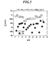
- the first voltage pulse for shifting the nanogap memory element from the low resistance state to the high resistance state and the second voltage pulse for shifting from the high resistance state to the low resistance state are repeatedly applied alternately. It is a graph which shows resistance value change.
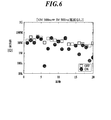
- the first voltage pulse for shifting the nanogap memory element from the low resistance state to the high resistance state and the second voltage pulse for shifting from the high resistance state to the low resistance state are repeatedly applied alternately. It is a graph which shows resistance value change.
- the first voltage pulse for shifting the nanogap memory device from the low resistance state to the high resistance state and the low resistance state from the high resistance state in another example having the same configuration as the embodiment and changing only the width of the pulse applied to the memory device. It is a graph which shows the resistance value change of an element at the time of applying repeatedly the 2nd voltage pulse made to shift to a resistance state alternately.
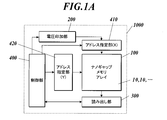
- the storage device 1000 is a device that stores data, including a memory element array in which a plurality of memory cells 110 are arranged in an array.
- the memory cell 110 includes the nanogap memory element 10 and the MOS transistor 11 as the selection element, and the memory element array is the nanogap memory array 100.
- the storage device 1000 includes a nanogap memory array 100, a voltage application unit 200, a reading unit 300, a control unit 400, and memory cells 110 arranged in an array.
- the nanogap memory array 100 is, for example, a high-density memory in which a plurality of memory cells 110 are arranged in an array (for example, a two-dimensional array).
- the memory cell 110 includes a MOS transistor 11 and a nanogap memory element 10 connected to the drain electrode or the source electrode of the MOS transistor 11.
- the MOS transistor 11 has a source electrode or a drain electrode connected to the X-direction addressing unit 410 and a gate electrode connected to the Y-direction addressing unit 420.
- the nanogap memory element 10 is, for example, a memory element that stores data by switching the resistance value between nanogap electrodes (the gap between the interelectrode gaps 4).
- the nanogap memory element 10 includes, for example, an insulating substrate 1, and a first electrode 2 and a second electrode 3 provided on one surface (upper surface) of the insulating substrate 1, as shown in FIG. And an inter-electrode gap 4 provided between the first electrode 2 and the second electrode 3.
- the insulating substrate 1 functions as a support for providing, for example, two electrodes (the first electrode 2 and the second electrode 3) of the nanogap memory element 10 apart from each other.
- the structure and material of the insulating substrate 1 are not particularly limited. Specifically, for example, the shape of the surface of the insulating substrate 1 may be a flat surface or may have irregularities. Further, the insulating substrate 1 may be, for example, a substrate in which an oxide film or the like is provided on the surface of a semiconductor substrate such as Si, or the substrate itself may be insulative.
- an oxide such as silicon oxide (SiO 2 ), a nitride such as silicon nitride (SiN), or the like is preferable.
- silicon oxide (SiO 2 ) is the first. This is suitable in terms of the high adhesion between the electrode 2 and the second electrode 3 and the degree of freedom in manufacturing.
- the first electrode 2 is paired with the second electrode 3 to perform the switching operation of the nanogap memory element 10.
- the shape of the 1st electrode 2 is not specifically limited, It can change arbitrarily arbitrarily.
- the material of the first electrode 2 is not particularly limited as long as it has conductivity. For example, gold, silver, platinum, palladium, nickel, aluminum, cobalt, chromium, rhodium, copper, tungsten, tantalum, carbon Or it is preferable that it is at least 1 chosen from these alloys.
- the first electrode 2 may be used by stacking two or more layers of different metals. Specifically, for example, the first electrode 2 may have a laminated (multilayer) structure of chromium and gold.
- the second electrode 3 is paired with the first electrode 2 to perform the switching operation of the nanogap memory element 10.
- the shape of the 2nd electrode 3 is not specifically limited, It can change arbitrarily arbitrarily.
- the material of the second electrode 3 is not particularly limited as long as it has conductivity. For example, gold, silver, platinum, palladium, nickel, aluminum, cobalt, chromium, rhodium, copper, tungsten, tantalum, carbon Or it is preferable that it is at least 1 chosen from these alloys.
- two or more layers of different metals may be used as the second electrode 3.
- the second electrode 3 may have a laminated (multilayer) structure of chromium and gold.
- the interelectrode gap 4 is formed, for example, between the first electrode 2 and the second electrode 3, and has a role of causing a resistance value change phenomenon of the nanogap memory element 10.
- the interelectrode gap 4 has a gap on the order of nanometers in which a switching phenomenon of resistance occurs when a predetermined voltage is applied between the first electrode 2 and the second electrode 3, for example. That is, the distance (interval) G between the first electrode 2 and the second electrode 3 (between nanogap electrodes) is set to be on the order of nanometers.
- the distance (interval) G between the first electrode 20 and the second electrode 30 (between nanogap electrodes) is preferably, for example, 0 nm ⁇ G ⁇ 13 nm, and 0.8 nm ⁇ G ⁇ 2.2 nm. More preferred.
- the reason why the upper limit value of the distance G is set to 13 nm is that, for example, when the gap G is formed by oblique deposition, switching does not occur when the gap interval is larger than 13 nm. Further, when typical values of the low resistance state and the high resistance state are substituted into the theoretical formula of the tunnel current, a range of 0.8 nm ⁇ G ⁇ 2.2 nm is obtained as a calculation result of the gap width.
- the nearest part (gap of the interelectrode gap part 4) between the first electrode 2 and the second electrode 3 is, for example, one or a plurality of places in a region where the first electrode 2 and the second electrode 3 face each other. It may be formed.
- the island part (Nakasu part) which consists of the constituent material of the said 1st electrode 2 and the 2nd electrode 3 etc. may be formed, for example.
- a predetermined gap (a gap between the interelectrode gap portions 4) is formed between the first electrode 2 and the island portion, and between the second electrode 3 and the island portion, so that the first electrode 2 As long as the second electrode 3 is not short-circuited.
- the voltage application unit 200 is connected to, for example, the plurality of memory cells 110 included in the nanogap memory array 100 and the control unit 400.
- the voltage application unit 200 applies a voltage (voltage pulse) between the first electrode 2 and the second electrode 3 of the nanogap memory element 10 in the memory cell 110 according to a control signal input from the control unit 400.
- a voltage voltage pulse
- data is written into the nanogap memory device 10 or data is erased from the nanogap memory device 10.
- address information related to the location of the nanogap memory element 10 to which a voltage pulse is applied is input from the control unit 400 to the voltage application unit 200.
- the voltage application unit 200 applies a voltage to the nanogap memory element 10 specified by the address information among the plurality of nanogap memory elements 10 included in the nanogap memory array 100, for example. A pulse is applied.
- the voltage application unit 200 has a resistance state between each of the first electrode 2 and the second electrode 3 between the low resistance state and the high resistance state for each nanogap memory element 10.
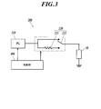
- the configuration shown in FIG. 3 is provided. That is, the voltage application unit 200 includes a pulse generator 210 as a pulse generation source that generates a voltage pulse with a predetermined voltage and a predetermined pulse width with respect to the memory element 10, and the pulse generator 210 and the nanogap memory element 10.
- the switching part 220 which can switch the 1st electrode 2 of a 1st connection state and a 2nd connection state is provided.
- the pulse generator 210 and the switching unit 220 are provided so as to be connected to each nanogap memory element 10 via the X-direction address specifying unit 410. It should be noted that each address specifying unit 410 and the MOS transistor 11 are actually interposed between the voltage applying unit 200 and each nanogap memory element 10, but these are not shown in FIG.
- the pulse generator 210 can output a single voltage pulse, and the control unit 400 can arbitrarily control the voltage and the pulse width.
- the switching unit 220 includes a path that forms a first connection state that directly connects the pulse generator 210 and the first electrode 2 of the nanogap memory element 10, and the first electrode of the pulse generator 210 and the nanogap memory element 10. 2 and a path that forms a second connection state connecting the two via the resistance element 221 as a resistor arranged in series with the switching element 222, and any one path is selectively selected by the switching element 222 It is possible to connect.
- the switching element 222 is controlled to be switched by the control unit 400.
- the voltage pulse output from the pulse generator 210 is directly applied to the nanogap memory device 10 as the first voltage pulse.
- the voltage pulse output from the pulse generator 210 is passed through the resistance element 222 to the nanogap memory element 10 as the second voltage pulse. Applied.
- the resistance value is inversely proportional to the total resistance value of the resistance element 222 and the nanogap memory element 10 with respect to the voltage pulse.
- the nanogap memory element 10 can be fixed to a resistance value that is as low as possible within a range that can be fixed.
- element destruction such as disconnection due to a rapid increase in element inflow current is prevented.
- the X-direction addressing unit 410 is a wiring in which the source electrodes of the MOS transistors 11 of the plurality of memory cells 110 arranged in the Y direction among the plurality of memory cells 110 provided in an array are connected in parallel. And each wiring is provided side by side in the X direction. And it is possible to apply the voltage pulse from the voltage application part 200 with respect to each wiring separately.
- the Y-direction address specification unit 420 is a wiring in which the gate electrodes of the MOS transistors 11 of the plurality of memory cells 110 arranged in the X direction among the plurality of memory cells 110 provided in an array are connected in parallel. And each wiring is provided side by side in the Y direction.
- a voltage as a designation signal can be individually applied to each wiring, thereby enabling connection of a source electrode and a drain electrode to each MOS transistor 11. That is, a designation signal is applied to the corresponding wiring in accordance with the position designation with respect to the address designation unit 420 in the Y direction, and a voltage pulse is applied to the corresponding wiring in accordance with the position designation with respect to the address designation unit 410 in the X direction.
- the memory cell 110 has a configuration in which at least a resistor is connected to the nanogap memory element 10 (and the MOS transistor 11 is further connected), thereby speeding up writing. This is because the charge / discharge current of the wiring leading to the memory cell 110 is not limited by the resistor.
- the memory cell area may increase, an increase in the memory cell area can be avoided if the resistor and the electrode of the memory element can be stacked. In this case, the switching unit 220 shown in FIG. 3 is unnecessary, and the memory cell can be voltage-driven from the pulse generator 210.
- the reading unit 300 is connected to the plurality of nanogap memory elements 10 included in the nanogap memory array 100 and the control unit 400. For example, the reading unit 300 reads data from the nanogap memory element 10 in accordance with a control signal input from the control unit 400 and outputs the read result to the control unit 400.
- address information regarding the location of the nanogap memory element 10 from which data is read is input from the control unit 400 to the reading unit 300.
- the reading unit 300 for example, out of the plurality of nanogap memory elements 10 included in the nanogap memory array 100, the nanogap electrode of the nanogap memory element 10 specified by the address information.
- Data is read from the nanogap memory element 10 by measuring the resistance value between the gaps (the gaps between the interelectrode gaps 4).
- the control unit 400 inputs a control signal (voltage value information, etc.) to the pulse generator 210 of the voltage application unit 200, and inputs an address signal to the address designation units 410, 420 in the X direction and Y direction,
- the nanogap memory element 10 is controlled so as to apply a voltage pulse having a predetermined pulse width with a predetermined voltage value.
- the control unit 400 switches the nanogap memory element 10 from a low resistance state (hereinafter also referred to as “ON state”) to a high resistance state (hereinafter also referred to as “OFF state”).
- the pulse generator 210 After controlling the switching element 222 so that the switching unit 220 is in the first connection state, the pulse generator 210 generates a pulse with the set voltage, and the first voltage pulse is applied to the nanogap memory element 10. To control. Further, when switching the nanogap memory element 10 from the high resistance state (OFF state) to the low resistance state (ON state), the switching element 222 is set so that the switching unit 220 is in the second connection state. After the control, the pulse generation vibrator 210 generates a pulse in the same manner as the first voltage pulse, and controls the second voltage pulse to be applied to the nanogap memory device 10.
- control unit 400 inputs a control signal (address information or the like) to the reading unit 300 to read data from the nanogap memory element 10, and Based on the read result, it is determined whether or not the nanogap memory device 10 has shifted from the high resistance state to the low resistance state. As a result of the determination, when the nanogap memory element 10 has not shifted from the high resistance state to the low resistance state, control may be performed so as to retry application of the second voltage pulse.
- the nanogap memory element 10A of Modification 1 is provided with an insulating substrate 1A, an insulator 5A provided on the upper surface of the insulating substrate 1A, and an upper surface of the insulating substrate 1A.
- the first electrode 2A, the second electrode 3A provided on the upper surface of the insulator 5A, and the interelectrode gap 4A provided between the first electrode 2A and the second electrode 3A are mainly provided.
- the insulator 5A is provided on the upper surface of the insulating substrate 1A to form a stepped portion, and the insulator 5A causes the first electrode 2A and the second electrode 3A to have a difference in height between the substrate 1A and the substrate 1A.
- the first electrode 2A is provided in contact with the upper surface of the insulating substrate 1A and the lower portion of the side surface 51A of the insulator 5A
- the second electrode 3A includes the upper surface of the insulator 5A and the insulator 5A. It is provided in contact with the upper part of the side surface 51A.
- the interelectrode gap 4A is provided between the first electrode 2A provided at the lower portion of the side surface 51A of the insulator 5A and the second electrode 3A provided at the upper portion of the side surface 51A of the insulator 5A. Is provided. That is, the gap G is formed in the interelectrode gap 4A along the height direction of the step formed by the insulator 5A.
- the insulator 5A is arranged so that the facing portion of the first electrode 2A and the facing portion of the second electrode 3A constituting the interelectrode gap 4A are aligned along the height direction with respect to the plane of the substrate 1A. Is. Therefore, other structures may be adopted as long as the above functions are provided.
- the insulator 5A may be, for example, a part of the insulating substrate 1A provided with an oxide film or the like, or may be provided with an oxide film or the like on the entire surface of the insulating substrate 1A, and a part thereof is removed.
- the insulator 5A for example, glass, oxides such as silicon oxide (SiO 2 ), nitrides such as silicon nitride (Si 3 N 4 ), and the like are preferable, and among these, silicon oxide (SiO 2 ) However, it is suitable in that the adhesion between the first electrode 2A and the second electrode 3A and the degree of freedom in the production are large.
- oxides such as silicon oxide (SiO 2 ), nitrides such as silicon nitride (Si 3 N 4 ), and the like are preferable, and among these, silicon oxide (SiO 2 )
- SiO 2 silicon oxide
- the inter-electrode gap 4A has substantially the same actual structure except that the orientation of the plane formed is different from that of the inter-electrode gap 4 described above. Therefore, the design conditions such as the dimensions of the interelectrode gap 4A and the operation method thereof are the same as those of the interelectrode gap 4 described above.
- the memory element 10A of the first modification has the same technical effect as that of the memory element 10 described above, and the first electrode 2A and the first electrode 2A are formed by a step formed by the insulator 5A on the upper surface of the insulating substrate 1A. Since the second electrode 3A is arranged with a height difference and the interelectrode gap 4A is formed along the height direction, the first electrode 2A, the second electrode 3A, and the interelectrode gap 4A are on the same plane. Compared with the case where the electrodes are arranged side by side, the inter-electrode gap 4A can reduce the area occupied by the insulating substrate 1A in plan view. Accordingly, for example, when a memory element is formed by integrating a large number of memory elements 10A while sharing a single insulating substrate 1A, it is advantageous for integration and the memory element can be reduced in size. Is possible.
- the nanogap memory element 10 may be employed.
- the first voltage pulse and the second voltage pulse are repeatedly applied alternately to the nanogap memory element 10A, and the resistance between the nanogap electrodes of the nanogap memory element 10A (the gap between the interelectrode gaps 4A) is changed. Values were measured after application of each voltage pulse.
- the voltage of the voltage pulse generated from the pulse generator 210 is 10 V
- the pulse width (application time of one voltage pulse) is 100 ⁇ s. did.
- the resistance element of the switching unit 220 in the voltage application unit 200 is 1 M ⁇ .
- the pulse generator 210 is directly connected to the nanogap memory element 10 without using the switching unit 220 for the same nanogap memory element 10A, and the applied voltage of the second voltage pulse is set to the first voltage pulse.
- the first voltage pulse and the second voltage pulse are alternately and repeatedly applied, and the gap between the nanogap electrodes of the nanogap memory element 10A at that time (interelectrode gap portion) 4A gap) was measured after application of each voltage pulse.
- the first voltage pulse was set to 10 V
- the second voltage pulse was set to 5 V
- the pulse widths were all 500 ns.
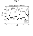
- FIG. 5 is a graph showing resistance values for each application of the first voltage pulse and the second voltage pulse in the embodiment
- FIG. 6 is for each application of the first voltage pulse and the second voltage pulse in the comparative example. It is a graph which shows the resistance value of.
- ⁇ indicates the resistance value when the first voltage pulse is applied (OFF)
- ⁇ indicates the resistance value when the second voltage pulse is applied (ON).
- the resistance value increases when the first voltage pulse is applied, and the resistance value tends to decrease when the second voltage pulse is applied.
- the high resistance state is often not switched to the sufficiently low resistance state.
- the resistance value of the nanogap memory element 10A after application of the first voltage pulse and the resistance value of the nanogap memory element 10A after application of the second voltage pulse are Variations are suppressed to be small, and there is almost no overlap between the numerical value range of the resistance in the high resistance state and the numerical value range of the resistance in the low resistance state. That is, it can be seen that by setting a certain threshold value, it is possible to more reliably identify whether the nanogap memory element 10A is in the ON state or the OFF state, and the practicality as a storage device is improved.
- the measurement result of the resistance value of the element 10A is shown.
- the resistance value of the nanogap memory element 10A after application of the first voltage pulse and the resistance value of the nanogap memory element 10A after application of the second voltage pulse are respectively shown.
- the variation is kept small, the numerical range of the resistance in the high resistance state and the numerical range of the resistance in the low resistance state are well separated, and the ON state and the OFF state of the nanogap memory element 10A can be easily distinguished. It can be seen that the practicality as a storage device is improved.
- the first voltage pulse is directly applied from the pulse generator 210 to the nanogap memory element 10 (or 10A) in the switching unit 220 of the voltage application unit 200.
- the second voltage pulse is applied through a resistance element 221 connected in series.
- a smaller current can be applied to the nanogap memory element 10 (or 10A).
- the nanogap memory element 10 (or 10A) as a memory element.
- the output voltage of the pulse generator can be kept constant. It is possible to apply a stable voltage.
- a part for example, the nanogap memory array 100 or the whole of the storage device 1000 may be sealed with a predetermined sealing member so that the interelectrode gap 4 does not come into contact with air or moisture. .
- the nanogap memory element 10 (or 10A) can be operated more stably.
- sealing with a predetermined sealing member it is possible to keep the interelectrode gap 4 in an arbitrary atmosphere and use the nanogap memory element 10 (or 10A) in an arbitrary atmosphere. can do.
- the voltage values and pulse widths of the first and second voltage pulses can be appropriately changed according to the gap size of the nanogap memory element, the electrode selection material, the atmosphere components between the gaps, and the like.
- the resistance value of the resistance element 221 is not strictly limited to 1 M ⁇ , but is also effective in the range of 3 M ⁇ to 0.3 M ⁇ , more preferably in the range of 1 M ⁇ from 2 M ⁇ to 0.5 M ⁇ .
- the voltage values of the first and second voltage pulses, the resistance value of the nanogap memory element at the time of high resistance and low resistance, etc. can be appropriately selected, and are limited to the above example. It is not something.
- the storage device 1000 the case where data is stored in the nanogap memory array 100 is illustrated, but the nanogap memory element 10 as a single unit, the voltage application unit 200, the reading unit 300, and the control unit 400 corresponding thereto.
- the device may be a storage device.
- the voltage application unit 200 applies only the second voltage pulse via the resistance element 221.
- the first voltage pulse is also applied via the resistance element. It is also good.
- the resistance element used when applying the first voltage pulse is selected to have a lower resistance value than the resistance element 221 used when applying the second voltage pulse, and the nanogap is applied when applying the first voltage pulse. The value of the current flowing through the memory element 10 is adjusted so as to be larger than when the second voltage pulse is applied.
Landscapes
- Semiconductor Memories (AREA)
Priority Applications (2)
| Application Number | Priority Date | Filing Date | Title |
|---|---|---|---|
| US13/819,217 US9135990B2 (en) | 2010-08-26 | 2011-08-25 | Drive method for memory element, and storage device using memory element |
| CN2011800413598A CN103081016A (zh) | 2010-08-26 | 2011-08-25 | 存储元件的驱动方法及使用存储元件的存储装置 |
Applications Claiming Priority (2)
| Application Number | Priority Date | Filing Date | Title |
|---|---|---|---|
| JP2010189132A JP5527729B2 (ja) | 2010-08-26 | 2010-08-26 | メモリ素子の駆動方法及びメモリ素子を備える記憶装置 |
| JP2010-189132 | 2010-08-26 |
Publications (1)
| Publication Number | Publication Date |
|---|---|
| WO2012026506A1 true WO2012026506A1 (ja) | 2012-03-01 |
Family
ID=45723498
Family Applications (1)
| Application Number | Title | Priority Date | Filing Date |
|---|---|---|---|
| PCT/JP2011/069113 Ceased WO2012026506A1 (ja) | 2010-08-26 | 2011-08-25 | メモリ素子の駆動方法及びメモリ素子を用いた記憶装置 |
Country Status (5)
| Country | Link |
|---|---|
| US (1) | US9135990B2 (https=) |
| JP (1) | JP5527729B2 (https=) |
| CN (1) | CN103081016A (https=) |
| TW (1) | TW201230036A (https=) |
| WO (1) | WO2012026506A1 (https=) |
Families Citing this family (1)
| Publication number | Priority date | Publication date | Assignee | Title |
|---|---|---|---|---|
| TWI624837B (zh) * | 2017-05-22 | 2018-05-21 | 旺宏電子股份有限公司 | 記憶體操作方法及記憶體操作裝置 |
Citations (4)
| Publication number | Priority date | Publication date | Assignee | Title |
|---|---|---|---|---|
| WO2006137111A1 (ja) * | 2005-06-20 | 2006-12-28 | Fujitsu Limited | 不揮発性半導体記憶装置及びその書き込み方法 |
| JP2007123828A (ja) * | 2005-09-27 | 2007-05-17 | National Institute Of Advanced Industrial & Technology | スイッチング素子 |
| WO2009034687A1 (ja) * | 2007-09-10 | 2009-03-19 | Panasonic Corporation | 不揮発性記憶装置および不揮発性記憶装置へのデータ書込方法 |
| JP2009205709A (ja) * | 2008-02-26 | 2009-09-10 | Funai Electric Advanced Applied Technology Research Institute Inc | ナノギャップ素子の駆動方法及びナノギャップ素子を備える記憶装置 |
Family Cites Families (7)
| Publication number | Priority date | Publication date | Assignee | Title |
|---|---|---|---|---|
| US7423787B2 (en) * | 2001-03-01 | 2008-09-09 | Ricoh Company, Ltd. | Optical scanning module, device, and method, and imaging apparatus |
| US7443710B2 (en) | 2004-09-28 | 2008-10-28 | Spansion, Llc | Control of memory devices possessing variable resistance characteristics |
| WO2007074504A1 (ja) | 2005-12-26 | 2007-07-05 | Fujitsu Limited | 不揮発性半導体記憶装置及びその書き込み方法 |
| JP5312782B2 (ja) * | 2007-12-20 | 2013-10-09 | 株式会社船井電機新応用技術研究所 | ナノギャップスイッチング素子の駆動方法及びナノギャップスイッチング素子を備える記憶装置 |
| JP4544340B2 (ja) * | 2008-01-24 | 2010-09-15 | ソニー株式会社 | 電子素子およびその製造方法並びに記憶装置 |
| JP2010157568A (ja) | 2008-12-26 | 2010-07-15 | Funai Electric Advanced Applied Technology Research Institute Inc | メモリセルアレイ |
| US8624217B2 (en) * | 2010-06-25 | 2014-01-07 | International Business Machines Corporation | Planar phase-change memory cell with parallel electrical paths |
-
2010
- 2010-08-26 JP JP2010189132A patent/JP5527729B2/ja not_active Expired - Fee Related
-
2011
- 2011-08-25 CN CN2011800413598A patent/CN103081016A/zh active Pending
- 2011-08-25 US US13/819,217 patent/US9135990B2/en not_active Expired - Fee Related
- 2011-08-25 WO PCT/JP2011/069113 patent/WO2012026506A1/ja not_active Ceased
- 2011-08-26 TW TW100130671A patent/TW201230036A/zh unknown
Patent Citations (4)
| Publication number | Priority date | Publication date | Assignee | Title |
|---|---|---|---|---|
| WO2006137111A1 (ja) * | 2005-06-20 | 2006-12-28 | Fujitsu Limited | 不揮発性半導体記憶装置及びその書き込み方法 |
| JP2007123828A (ja) * | 2005-09-27 | 2007-05-17 | National Institute Of Advanced Industrial & Technology | スイッチング素子 |
| WO2009034687A1 (ja) * | 2007-09-10 | 2009-03-19 | Panasonic Corporation | 不揮発性記憶装置および不揮発性記憶装置へのデータ書込方法 |
| JP2009205709A (ja) * | 2008-02-26 | 2009-09-10 | Funai Electric Advanced Applied Technology Research Institute Inc | ナノギャップ素子の駆動方法及びナノギャップ素子を備える記憶装置 |
Also Published As
| Publication number | Publication date |
|---|---|
| JP5527729B2 (ja) | 2014-06-25 |
| TW201230036A (en) | 2012-07-16 |
| US20130155757A1 (en) | 2013-06-20 |
| US9135990B2 (en) | 2015-09-15 |
| CN103081016A (zh) | 2013-05-01 |
| JP2012048779A (ja) | 2012-03-08 |
Similar Documents
| Publication | Publication Date | Title |
|---|---|---|
| CN101681913B (zh) | 可变电阻元件及其制造方法和非易失性半导体存储装置 | |
| JP5352032B2 (ja) | 不揮発性記憶素子および不揮発性記憶装置 | |
| KR101593509B1 (ko) | 이종 접합 산화물을 기반으로 하는 멤리스티브 요소 | |
| US20130301341A1 (en) | Hereto resistive switching material layer in rram device and method | |
| US8957399B2 (en) | Nonvolatile memory element and nonvolatile memory device | |
| US20130292630A1 (en) | Semiconductor memory device | |
| US8854864B2 (en) | Nonvolatile memory element and nonvolatile memory device | |
| JP2014523637A (ja) | 非線形素子を有するスイッチングデバイス | |
| JP2015220465A (ja) | 抵抗性メモリアーキテクチャ及び装置 | |
| US9343144B2 (en) | Memory device and method of controlling memory device | |
| JP2011199215A (ja) | 半導体記憶装置 | |
| JPWO2015114825A1 (ja) | 半導体記憶装置 | |
| JP5216254B2 (ja) | メモリ素子アレイ | |
| JP5312782B2 (ja) | ナノギャップスイッチング素子の駆動方法及びナノギャップスイッチング素子を備える記憶装置 | |
| JP5527729B2 (ja) | メモリ素子の駆動方法及びメモリ素子を備える記憶装置 | |
| JP5499364B2 (ja) | メモリ素子の駆動方法及びメモリ素子を備える記憶装置 | |
| CN101322195B (zh) | 具有存储矩阵的电子电路 | |
| JP2013197172A (ja) | 抵抗変化メモリ | |
| CN104752607A (zh) | 阻变存储器及其制备方法 | |
| JP5553797B2 (ja) | 半導体記憶装置のデータ記録方法 | |
| JP2012119566A (ja) | 半導体装置およびその製造方法 | |
| KR20200083908A (ko) | 변동 저저항 영역 기반 메모리 소자 및 이의 제어 방법 | |
| WO2003075360A1 (fr) | Element a effet de commutation magnetoresistant et dispositif magnetoresistant comprenant cet element |
Legal Events
| Date | Code | Title | Description |
|---|---|---|---|
| WWE | Wipo information: entry into national phase |
Ref document number: 201180041359.8 Country of ref document: CN |
|
| 121 | Ep: the epo has been informed by wipo that ep was designated in this application |
Ref document number: 11819969 Country of ref document: EP Kind code of ref document: A1 |
|
| NENP | Non-entry into the national phase |
Ref country code: DE |
|
| WWE | Wipo information: entry into national phase |
Ref document number: 13819217 Country of ref document: US |
|
| 122 | Ep: pct application non-entry in european phase |
Ref document number: 11819969 Country of ref document: EP Kind code of ref document: A1 |