WO2012018024A1 - プラズマ処理装置 - Google Patents
プラズマ処理装置 Download PDFInfo
- Publication number
- WO2012018024A1 WO2012018024A1 PCT/JP2011/067698 JP2011067698W WO2012018024A1 WO 2012018024 A1 WO2012018024 A1 WO 2012018024A1 JP 2011067698 W JP2011067698 W JP 2011067698W WO 2012018024 A1 WO2012018024 A1 WO 2012018024A1
- Authority
- WO
- WIPO (PCT)
- Prior art keywords
- plasma
- chamber
- plasma processing
- processing apparatus
- gas
- Prior art date
Links
- 238000009832 plasma treatment Methods 0.000 title abstract 6
- 238000012545 processing Methods 0.000 claims description 162
- 239000000463 material Substances 0.000 claims description 9
- 238000004891 communication Methods 0.000 claims description 3
- 238000010494 dissociation reaction Methods 0.000 abstract description 15
- 230000005593 dissociations Effects 0.000 abstract description 14
- 238000009826 distribution Methods 0.000 abstract description 12
- 230000007246 mechanism Effects 0.000 abstract description 7
- 238000004519 manufacturing process Methods 0.000 abstract description 6
- 239000007789 gas Substances 0.000 description 59
- 239000010408 film Substances 0.000 description 20
- 239000000758 substrate Substances 0.000 description 20
- 238000005192 partition Methods 0.000 description 17
- 239000010409 thin film Substances 0.000 description 17
- -1 atomic hydrogen radicals Chemical class 0.000 description 15
- 238000000034 method Methods 0.000 description 10
- 229910000077 silane Inorganic materials 0.000 description 10
- 230000008569 process Effects 0.000 description 9
- XUIMIQQOPSSXEZ-UHFFFAOYSA-N Silicon Chemical compound [Si] XUIMIQQOPSSXEZ-UHFFFAOYSA-N 0.000 description 8
- 229910052710 silicon Inorganic materials 0.000 description 8
- 239000010703 silicon Substances 0.000 description 8
- 230000008859 change Effects 0.000 description 7
- 150000003254 radicals Chemical class 0.000 description 7
- BLRPTPMANUNPDV-UHFFFAOYSA-N Silane Chemical compound [SiH4] BLRPTPMANUNPDV-UHFFFAOYSA-N 0.000 description 6
- 230000015572 biosynthetic process Effects 0.000 description 6
- 230000007423 decrease Effects 0.000 description 6
- 239000001257 hydrogen Substances 0.000 description 6
- 229910052739 hydrogen Inorganic materials 0.000 description 6
- UFHFLCQGNIYNRP-UHFFFAOYSA-N Hydrogen Chemical compound [H][H] UFHFLCQGNIYNRP-UHFFFAOYSA-N 0.000 description 4
- 230000004048 modification Effects 0.000 description 4
- 238000012986 modification Methods 0.000 description 4
- IJGRMHOSHXDMSA-UHFFFAOYSA-N Atomic nitrogen Chemical compound N#N IJGRMHOSHXDMSA-UHFFFAOYSA-N 0.000 description 3
- 239000004020 conductor Substances 0.000 description 3
- 230000007547 defect Effects 0.000 description 3
- 238000009792 diffusion process Methods 0.000 description 3
- 238000005530 etching Methods 0.000 description 3
- 238000002474 experimental method Methods 0.000 description 3
- 229910021424 microcrystalline silicon Inorganic materials 0.000 description 3
- 239000000523 sample Substances 0.000 description 3
- QGZKDVFQNNGYKY-UHFFFAOYSA-N Ammonia Chemical compound N QGZKDVFQNNGYKY-UHFFFAOYSA-N 0.000 description 2
- 229910052782 aluminium Inorganic materials 0.000 description 2
- XAGFODPZIPBFFR-UHFFFAOYSA-N aluminium Chemical compound [Al] XAGFODPZIPBFFR-UHFFFAOYSA-N 0.000 description 2
- 238000006243 chemical reaction Methods 0.000 description 2
- 230000008878 coupling Effects 0.000 description 2
- 238000010168 coupling process Methods 0.000 description 2
- 238000005859 coupling reaction Methods 0.000 description 2
- 238000000354 decomposition reaction Methods 0.000 description 2
- 230000008021 deposition Effects 0.000 description 2
- 150000002431 hydrogen Chemical class 0.000 description 2
- 238000009616 inductively coupled plasma Methods 0.000 description 2
- 150000004767 nitrides Chemical class 0.000 description 2
- JLTRXTDYQLMHGR-UHFFFAOYSA-N trimethylaluminium Chemical compound C[Al](C)C JLTRXTDYQLMHGR-UHFFFAOYSA-N 0.000 description 2
- MYMOFIZGZYHOMD-UHFFFAOYSA-N Dioxygen Chemical compound O=O MYMOFIZGZYHOMD-UHFFFAOYSA-N 0.000 description 1
- YZCKVEUIGOORGS-UHFFFAOYSA-N Hydrogen atom Chemical compound [H] YZCKVEUIGOORGS-UHFFFAOYSA-N 0.000 description 1
- 230000009471 action Effects 0.000 description 1
- 229910021529 ammonia Inorganic materials 0.000 description 1
- 229910021417 amorphous silicon Inorganic materials 0.000 description 1
- 238000004380 ashing Methods 0.000 description 1
- 238000005452 bending Methods 0.000 description 1
- 238000004140 cleaning Methods 0.000 description 1
- 238000010586 diagram Methods 0.000 description 1
- 229910001882 dioxygen Inorganic materials 0.000 description 1
- 208000018459 dissociative disease Diseases 0.000 description 1
- 230000001939 inductive effect Effects 0.000 description 1
- 229910052751 metal Inorganic materials 0.000 description 1
- 239000002184 metal Substances 0.000 description 1
- 229910052757 nitrogen Inorganic materials 0.000 description 1
- 125000002524 organometallic group Chemical group 0.000 description 1
- 230000004044 response Effects 0.000 description 1
- 239000004065 semiconductor Substances 0.000 description 1
- 229910001220 stainless steel Inorganic materials 0.000 description 1
- 239000010935 stainless steel Substances 0.000 description 1
- 230000001629 suppression Effects 0.000 description 1
- 238000004804 winding Methods 0.000 description 1
Images


Classifications
-
- C—CHEMISTRY; METALLURGY
- C23—COATING METALLIC MATERIAL; COATING MATERIAL WITH METALLIC MATERIAL; CHEMICAL SURFACE TREATMENT; DIFFUSION TREATMENT OF METALLIC MATERIAL; COATING BY VACUUM EVAPORATION, BY SPUTTERING, BY ION IMPLANTATION OR BY CHEMICAL VAPOUR DEPOSITION, IN GENERAL; INHIBITING CORROSION OF METALLIC MATERIAL OR INCRUSTATION IN GENERAL
- C23C—COATING METALLIC MATERIAL; COATING MATERIAL WITH METALLIC MATERIAL; SURFACE TREATMENT OF METALLIC MATERIAL BY DIFFUSION INTO THE SURFACE, BY CHEMICAL CONVERSION OR SUBSTITUTION; COATING BY VACUUM EVAPORATION, BY SPUTTERING, BY ION IMPLANTATION OR BY CHEMICAL VAPOUR DEPOSITION, IN GENERAL
- C23C16/00—Chemical coating by decomposition of gaseous compounds, without leaving reaction products of surface material in the coating, i.e. chemical vapour deposition [CVD] processes
- C23C16/44—Chemical coating by decomposition of gaseous compounds, without leaving reaction products of surface material in the coating, i.e. chemical vapour deposition [CVD] processes characterised by the method of coating
- C23C16/50—Chemical coating by decomposition of gaseous compounds, without leaving reaction products of surface material in the coating, i.e. chemical vapour deposition [CVD] processes characterised by the method of coating using electric discharges
- C23C16/505—Chemical coating by decomposition of gaseous compounds, without leaving reaction products of surface material in the coating, i.e. chemical vapour deposition [CVD] processes characterised by the method of coating using electric discharges using radio frequency discharges
- C23C16/509—Chemical coating by decomposition of gaseous compounds, without leaving reaction products of surface material in the coating, i.e. chemical vapour deposition [CVD] processes characterised by the method of coating using electric discharges using radio frequency discharges using internal electrodes
-
- H—ELECTRICITY
- H01—ELECTRIC ELEMENTS
- H01L—SEMICONDUCTOR DEVICES NOT COVERED BY CLASS H10
- H01L21/00—Processes or apparatus adapted for the manufacture or treatment of semiconductor or solid state devices or of parts thereof
- H01L21/02—Manufacture or treatment of semiconductor devices or of parts thereof
- H01L21/02104—Forming layers
-
- H—ELECTRICITY
- H01—ELECTRIC ELEMENTS
- H01J—ELECTRIC DISCHARGE TUBES OR DISCHARGE LAMPS
- H01J37/00—Discharge tubes with provision for introducing objects or material to be exposed to the discharge, e.g. for the purpose of examination or processing thereof
- H01J37/32—Gas-filled discharge tubes
- H01J37/32009—Arrangements for generation of plasma specially adapted for examination or treatment of objects, e.g. plasma sources
- H01J37/32082—Radio frequency generated discharge
- H01J37/321—Radio frequency generated discharge the radio frequency energy being inductively coupled to the plasma
- H01J37/3211—Antennas, e.g. particular shapes of coils
-
- H—ELECTRICITY
- H01—ELECTRIC ELEMENTS
- H01J—ELECTRIC DISCHARGE TUBES OR DISCHARGE LAMPS
- H01J37/00—Discharge tubes with provision for introducing objects or material to be exposed to the discharge, e.g. for the purpose of examination or processing thereof
- H01J37/32—Gas-filled discharge tubes
- H01J37/32009—Arrangements for generation of plasma specially adapted for examination or treatment of objects, e.g. plasma sources
- H01J37/32357—Generation remote from the workpiece, e.g. down-stream
-
- H—ELECTRICITY
- H01—ELECTRIC ELEMENTS
- H01J—ELECTRIC DISCHARGE TUBES OR DISCHARGE LAMPS
- H01J37/00—Discharge tubes with provision for introducing objects or material to be exposed to the discharge, e.g. for the purpose of examination or processing thereof
- H01J37/32—Gas-filled discharge tubes
- H01J37/32009—Arrangements for generation of plasma specially adapted for examination or treatment of objects, e.g. plasma sources
- H01J37/32422—Arrangement for selecting ions or species in the plasma
-
- H—ELECTRICITY
- H01—ELECTRIC ELEMENTS
- H01J—ELECTRIC DISCHARGE TUBES OR DISCHARGE LAMPS
- H01J37/00—Discharge tubes with provision for introducing objects or material to be exposed to the discharge, e.g. for the purpose of examination or processing thereof
- H01J37/32—Gas-filled discharge tubes
- H01J37/32431—Constructional details of the reactor
- H01J37/32532—Electrodes
- H01J37/32568—Relative arrangement or disposition of electrodes; moving means
-
- H—ELECTRICITY
- H01—ELECTRIC ELEMENTS
- H01J—ELECTRIC DISCHARGE TUBES OR DISCHARGE LAMPS
- H01J37/00—Discharge tubes with provision for introducing objects or material to be exposed to the discharge, e.g. for the purpose of examination or processing thereof
- H01J37/32—Gas-filled discharge tubes
- H01J37/32431—Constructional details of the reactor
- H01J37/32623—Mechanical discharge control means
-
- H—ELECTRICITY
- H01—ELECTRIC ELEMENTS
- H01J—ELECTRIC DISCHARGE TUBES OR DISCHARGE LAMPS
- H01J37/00—Discharge tubes with provision for introducing objects or material to be exposed to the discharge, e.g. for the purpose of examination or processing thereof
- H01J37/32—Gas-filled discharge tubes
- H01J37/32431—Constructional details of the reactor
- H01J37/32798—Further details of plasma apparatus not provided for in groups H01J37/3244 - H01J37/32788; special provisions for cleaning or maintenance of the apparatus
- H01J37/32816—Pressure
- H01J37/32834—Exhausting
-
- H—ELECTRICITY
- H01—ELECTRIC ELEMENTS
- H01J—ELECTRIC DISCHARGE TUBES OR DISCHARGE LAMPS
- H01J37/00—Discharge tubes with provision for introducing objects or material to be exposed to the discharge, e.g. for the purpose of examination or processing thereof
- H01J37/32—Gas-filled discharge tubes
- H01J37/32431—Constructional details of the reactor
- H01J37/32798—Further details of plasma apparatus not provided for in groups H01J37/3244 - H01J37/32788; special provisions for cleaning or maintenance of the apparatus
- H01J37/32899—Multiple chambers, e.g. cluster tools
-
- H—ELECTRICITY
- H01—ELECTRIC ELEMENTS
- H01J—ELECTRIC DISCHARGE TUBES OR DISCHARGE LAMPS
- H01J37/00—Discharge tubes with provision for introducing objects or material to be exposed to the discharge, e.g. for the purpose of examination or processing thereof
- H01J37/32—Gas-filled discharge tubes
- H01J37/32917—Plasma diagnostics
- H01J37/32935—Monitoring and controlling tubes by information coming from the object and/or discharge
- H01J37/32954—Electron temperature measurement
-
- H—ELECTRICITY
- H01—ELECTRIC ELEMENTS
- H01L—SEMICONDUCTOR DEVICES NOT COVERED BY CLASS H10
- H01L21/00—Processes or apparatus adapted for the manufacture or treatment of semiconductor or solid state devices or of parts thereof
- H01L21/02—Manufacture or treatment of semiconductor devices or of parts thereof
- H01L21/04—Manufacture or treatment of semiconductor devices or of parts thereof the devices having potential barriers, e.g. a PN junction, depletion layer or carrier concentration layer
- H01L21/34—Manufacture or treatment of semiconductor devices or of parts thereof the devices having potential barriers, e.g. a PN junction, depletion layer or carrier concentration layer the devices having semiconductor bodies not provided for in groups H01L21/0405, H01L21/0445, H01L21/06, H01L21/16 and H01L21/18 with or without impurities, e.g. doping materials
- H01L21/46—Treatment of semiconductor bodies using processes or apparatus not provided for in groups H01L21/428
- H01L21/461—Treatment of semiconductor bodies using processes or apparatus not provided for in groups H01L21/428 to change their surface-physical characteristics or shape, e.g. etching, polishing, cutting
- H01L21/465—Chemical or electrical treatment, e.g. electrolytic etching
-
- H—ELECTRICITY
- H05—ELECTRIC TECHNIQUES NOT OTHERWISE PROVIDED FOR
- H05H—PLASMA TECHNIQUE; PRODUCTION OF ACCELERATED ELECTRICALLY-CHARGED PARTICLES OR OF NEUTRONS; PRODUCTION OR ACCELERATION OF NEUTRAL MOLECULAR OR ATOMIC BEAMS
- H05H1/00—Generating plasma; Handling plasma
- H05H1/24—Generating plasma
- H05H1/46—Generating plasma using applied electromagnetic fields, e.g. high frequency or microwave energy
- H05H1/4645—Radiofrequency discharges
- H05H1/4652—Radiofrequency discharges using inductive coupling means, e.g. coils
-
- C—CHEMISTRY; METALLURGY
- C23—COATING METALLIC MATERIAL; COATING MATERIAL WITH METALLIC MATERIAL; CHEMICAL SURFACE TREATMENT; DIFFUSION TREATMENT OF METALLIC MATERIAL; COATING BY VACUUM EVAPORATION, BY SPUTTERING, BY ION IMPLANTATION OR BY CHEMICAL VAPOUR DEPOSITION, IN GENERAL; INHIBITING CORROSION OF METALLIC MATERIAL OR INCRUSTATION IN GENERAL
- C23C—COATING METALLIC MATERIAL; COATING MATERIAL WITH METALLIC MATERIAL; SURFACE TREATMENT OF METALLIC MATERIAL BY DIFFUSION INTO THE SURFACE, BY CHEMICAL CONVERSION OR SUBSTITUTION; COATING BY VACUUM EVAPORATION, BY SPUTTERING, BY ION IMPLANTATION OR BY CHEMICAL VAPOUR DEPOSITION, IN GENERAL
- C23C16/00—Chemical coating by decomposition of gaseous compounds, without leaving reaction products of surface material in the coating, i.e. chemical vapour deposition [CVD] processes
- C23C16/22—Chemical coating by decomposition of gaseous compounds, without leaving reaction products of surface material in the coating, i.e. chemical vapour deposition [CVD] processes characterised by the deposition of inorganic material, other than metallic material
- C23C16/24—Deposition of silicon only
Definitions
- the present invention relates to a plasma processing apparatus for performing predetermined processing such as deposition (film formation) and etching on a substrate to be processed.
- a plasma processing apparatus has been used in a film forming process for forming a thin film on a substrate and an etching process for the substrate.
- plasma processing equipment such as capacitive coupling type and inductive coupling type.
- the inductively coupled plasma processing equipment is capable of generating high-density plasma and has a high processing speed. (For example, refer to Patent Document 1).
- Formation of a silicon thin film by a plasma processing apparatus is usually performed as follows. First, hydrogen (H 2 ) gas and silane (SiH 4 ) gas are introduced into a vacuum vessel, and plasma is generated in the vacuum vessel by applying discharge power. At this time, the hydrogen gas molecules and silane gas molecules collide with each other, and these molecules are decomposed, and the atomic hydrogen radicals and silane radicals (SiH 3 , SiH 2 , SiH, Si) generated thereby are stored in the vacuum vessel. Is diffused to reach the substrate surface, and a silicon thin film is formed on the substrate surface.
- hydrogen (H 2 ) gas and silane (SiH 4 ) gas are introduced into a vacuum vessel, and plasma is generated in the vacuum vessel by applying discharge power. At this time, the hydrogen gas molecules and silane gas molecules collide with each other, and these molecules are decomposed, and the atomic hydrogen radicals and silane radicals (SiH 3 , SiH 2 , SiH, Si) generated thereby are stored in the vacuum
- the energy of electrons required to dissociate molecules by electron collision is higher in the case of hydrogen molecules than in the case of SiH 4 molecules. Therefore, increasing the high-energy electrons for dissociating hydrogen molecules or increasing the plasma density causes significant dissociation of silane-based molecules at the same time as the generation of high-density atomic hydrogen radicals, and SiH 2 , SiH, A large number of radicals such as Si having a high adhesion coefficient, that is, easy to adhere to the microcrystalline silicon thin film being formed, are generated.
- the problem to be solved by the present invention is to provide a plasma processing apparatus capable of easily controlling the energy distribution of electrons in plasma according to the type of gas molecules and their dissociation energy.
- the plasma processing apparatus which has been made to solve the above problems, A plasma generation chamber; a high-frequency antenna provided in the plasma generation chamber; plasma generation gas introduction means for introducing a gas for generating plasma into the plasma generation chamber; and a plasma processing chamber in communication with the plasma generation chamber;
- a plasma processing apparatus comprising a processing gas introduction means for introducing a processing gas into the plasma processing chamber, A plasma control plate provided in the plasma generation chamber and capable of changing a distance from the high-frequency antenna; Moving means for moving the plasma control plate; It is characterized by providing.
- a differential pressure generating means for generating a differential pressure between the plasma generating chamber and the plasma processing chamber.
- the differential pressure generating means By making the pressure of the plasma generation chamber higher than that of the plasma processing chamber using the differential pressure generating means, it is possible to prevent the processing gas in the plasma processing chamber from entering the plasma generation chamber and dissociating the processing gas excessively. Can do.
- a plate material having a large number of through holes is provided at the boundary between the plasma generating chamber and the plasma processing chamber, or a processing gas which is the processing gas introducing means and has holes on the plasma processing chamber side A large number of introduction pipes arranged at the boundary between the plasma generation chamber and the plasma processing chamber with a gap may be used.
- the plasma processing apparatus can be provided with a plurality of plasma generation chambers in response to an increase in the area of the substrate to be processed.
- the plasma generation chamber is arranged at a certain interval on one wall surface of the plasma processing chamber, and an exhaust means for exhausting the plasma processing chamber between these plasma generation chambers and an exhaust amount for adjusting the exhaust amount. It is desirable to use a configuration in which adjusting means is provided. These exhaust means and exhaust amount adjusting means are for maintaining the time during which the processing gas introduced into the plasma processing chamber is present in the plasma processing chamber substantially constant, and by this, the plasma generated in the plasma generation chamber is used. It is possible to prevent the dissociation of the processing gas in the plasma processing chamber from proceeding excessively.
- the plasma processing apparatus controls the energy distribution of electrons in the plasma by adjusting the distance between the high-frequency antennas in the plasma generation chamber with a plasma control plate provided in the plasma generation chamber. is there.
- a plasma control plate provided in the plasma generation chamber.
- the plasma control plate is brought close to the high-frequency antenna, electrons in the plasma generated in the plasma generation chamber disappear due to collision with the plasma control plate, and the electron density decreases.
- This decrease in electron density reduces collisions between electrons in the plasma, leaving many high-energy electrons in the plasma.
- the energy distribution of electrons can be controlled simply by adjusting the distance between the plasma control plate and the high-frequency antenna. Using this, the degree of dissociation can be controlled according to the type of gas molecule.
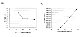
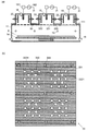
- FIG. 2 is a schematic longitudinal sectional view (a) and a schematic transverse sectional view (b) showing an experimental apparatus for examining a change in plasma characteristics with respect to a distance between a high frequency antenna and a plasma control plate.
- the graph (a) which shows the change of the electron temperature with respect to the distance between a high frequency antenna and a plasma control board, and the graph (b) which shows the change of an electron density.
- the graph (a) which shows the change of the energy distribution of the electron with respect to the distance between a high frequency antenna and a plasma control board, and the graph (b) which shows the change of the relative ratio.
- 1 is a schematic longitudinal sectional view showing a first embodiment of a plasma processing apparatus according to the present invention.
- the bottom view which shows the partition plate provided in the boundary of a plasma production chamber and a plasma processing chamber.
- the schematic longitudinal cross-sectional view which shows 2nd Example of the plasma processing apparatus which concerns on this invention.
- the schematic longitudinal cross-sectional view which shows 3rd Example of the plasma processing apparatus which concerns on this invention.
- the schematic longitudinal cross-sectional view which shows the 1st modification of the plasma processing apparatus of 3rd Example.
- the schematic longitudinal cross-sectional view (a) which shows the 2nd modification of the plasma processing apparatus of 3rd Example, and the bottom view (b) which shows the partition plate used by this modification.
- the inventor of the present application conducted an experiment on the change in plasma characteristics with respect to the distance between the high-frequency antenna and the plasma control plate, using the experimental apparatus shown in the schematic diagram of FIG.
- This experimental apparatus is made of stainless steel having a structure in which two cylindrical tubes having a diameter of 150 mm extending in the vertical (hereinafter referred to as “vertical” or “upper and lower”) direction and in the horizontal (hereinafter referred to as “lateral”) direction cross each other.
- Cross tube chamber 51 high-frequency antenna 52 made of a U-shaped conductor inserted into cross tube chamber 51 from one end of a cylindrical tube extending in the lateral direction of cross tube chamber 51, and the other end
- a Langmuir probe 53 for measuring various states of plasma inserted into the cross tube chamber 51 from the side, and arranged at equal intervals on both sides of the high-frequency antenna 52 280 mm in length, 97 mm in width, and 6 mm in thickness 2
- a plasma control plate 54 made of a single aluminum flat plate.
- the high-frequency antenna 52 is inserted in the chamber 51 with both ends of the U shape aligned vertically.
- a high-frequency power source 522 having a frequency of 13.56 MHz and a maximum output of 1250 W is connected to one end of the high-frequency antenna 52 via an impedance matching device 521, and the other end is grounded.
- the high frequency antenna 52 is covered with a dielectric pipe inside the chamber 51.
- the dimensions of the high frequency antenna 52 inside the chamber 51 are 55 mm long and 110 mm wide.
- the plasma control plate 54 is provided with an operation rod and a moving mechanism (not shown) extending in a direction perpendicular to the surface. Since the operation rod can be moved in the longitudinal direction by the moving mechanism, the distance between the plasma control plate 54 and the high frequency antenna 52 can be freely adjusted.
- an inlet for introducing a gas for generating plasma into the chamber 51 is provided in the upper part of the cylindrical tube extending in the vertical direction, and the exhaust for evacuating the chamber 51 is provided in the lower part. Mouth is provided.
- the change in plasma characteristics with respect to the distance D between the high-frequency antenna 52 and the plasma control plate 54 was examined.
- the experimental results are shown in FIGS.
- hydrogen was introduced as a plasma generation gas at a flow rate of 5 sccm
- the output of the high frequency power source was 800 W
- the pressure in the chamber 51 was 10 Pa.
- the plasma was measured with the distance between the tip of the Langmuir probe 53 and the high-frequency antenna 52 being 120 mm.
- the inventor of the present application has obtained knowledge that it is effective to adjust the distance from the high-frequency antenna using a plasma control plate for controlling the energy distribution of electrons in the plasma. Examples of the plasma processing apparatus according to the present invention will be described below.
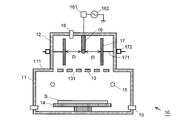
- FIG. 4 is a schematic longitudinal sectional view of a first embodiment of the plasma processing apparatus according to the present invention.
- the plasma processing apparatus 10 of this embodiment includes a plasma processing chamber 11 composed of a rectangular parallelepiped vacuum vessel and a plasma generator attached to a top plate (upper wall) 111 of the plasma processing chamber 11 composed of a rectangular parallelepiped vacuum vessel. Chamber 12.
- a partition plate 13 having a large number of through holes 131 for generating a differential pressure in the plasma processing chamber 11 and the plasma generation chamber 12 is disposed at the boundary between the plasma processing chamber 11 and the plasma generation chamber 12. Yes.
- a substrate table 14 for placing the substrate S is provided so as to face the partition plate 13.
- the substrate base 14 has a built-in heater, and the substrate S can be heated during the formation of the thin film as necessary.
- a processing gas inlet 15 for introducing a processing gas into the plasma processing chamber 11 is provided at a position between the partition plate 13 and the substrate base 14 in the plasma processing chamber 11.
- An exhaust port 19 for exhausting the plasma processing chamber is provided below the plasma processing chamber 11.
- a high frequency antenna 16 formed by bending a rod-like conductor into a U shape is provided. Both ends of the high-frequency antenna 16 are attached to the upper wall of the plasma generation chamber 12, and one end is connected to the high-frequency power source 162 via the impedance matching device 161 and the other end is grounded, as in the experimental apparatus of FIG. .
- two plasma control plates 17 are arranged at an equal distance from the high frequency antenna 16 so as to sandwich the high frequency antenna 16.
- An operation rod 171 is attached to the plasma control plate 17, and the operation rod 171 can be moved in the longitudinal direction by the moving mechanism 172.
- the distance between the plasma control plate 17 and the high-frequency antenna 16 can be adjusted by the action of the operation rod 171 and the moving mechanism 172 which are moving means of the control plate 17.
- a plasma generation gas inlet 18 for introducing a plasma generation gas into the chamber is provided on the wall of the plasma generation chamber 12.
- the operation of the plasma processing apparatus 10 of the first embodiment will be described by taking as an example the case of generating a silicon thin film.
- hydrogen (H 2 ) gas is introduced into the plasma generation chamber 12 as a plasma generation gas from the plasma generation gas inlet 18, and SiH 4 gas is supplied into the plasma processing chamber 11 as a processing gas from the processing gas inlet 15.
- a gas containing is introduced.
- the pressure in the plasma processing chamber 11 is set to 1 Pa or less, and the pressure in the plasma generation chamber 12 is set to 2 Pa higher than that in the plasma processing chamber 11.
- the processing gas (SiH 4 gas) introduced into the plasma processing chamber 11 passes through the through holes of the partition plate 13 and enters the plasma generation chamber 12. It can be prevented from entering.
- high frequency power having a frequency of 13.56 MHz and a power of 1000 W is input to the high frequency antenna 16.
- plasma containing atomic hydrogen radicals and electrons is generated in the plasma generation chamber 12.
- the plasma generated in the plasma generation chamber 12 passes through the through hole of the partition plate 13 and diffuses into the plasma processing chamber 11.
- the plasma diffused from the plasma generation chamber 12 is introduced from the processing gas inlet 15.
- SiH 4 gas is decomposed to generate silane radicals containing SiH 3 .
- a silicon thin film is formed on the substrate S by the hydrogen radicals generated in the plasma generation chamber and passing through the through holes of the partition plate 13 and the silane-based radicals generated in the plasma processing chamber.
- the temperature of the substrate S is maintained at 200 ° C. by the heater.
- plasma generation is performed by adjusting the distance between the plasma control plate 17 and the high frequency antenna 16.
- the energy distribution of electrons in the plasma in the chamber 12 can be controlled.
- the percentage of electrons in the high energy region increases by bringing the plasma control plate 17 closer to the high frequency antenna 16. For this reason, generation of atomic hydrogen radicals can be promoted.
- the electron temperature of the plasma can be finely adjusted so that the radical dissociation reaction does not proceed excessively.
- a function peculiar to the plasma processing apparatus 10 of the present embodiment which is difficult to realize with the conventional plasma processing apparatus, is that a plasma generation chamber is provided between the plasma generation chamber 12 and the plasma processing chamber 11 via a partition plate 13.
- the SiH 4 gas introduced into the plasma processing chamber 11 flows back into the plasma generation chamber 12 with a high proportion of high-energy electrons and flows into the plasma generation chamber 12. It is possible to suppress passing the region near the antenna 16 and excessive dissociation of SiH 4 molecules.
- the energy distribution of electrons in the diffusion plasma in which the plasma generated in the plasma generation chamber 12 is introduced into the plasma processing chamber 11 via the partition plate 13 is the plasma generated in the plasma generation chamber 12.
- a plasma generation chamber 12 that is a reaction region that generates atomic hydrogen radicals by dissociation of H 2 gas and a plasma processing chamber 11 that is a reaction region that dissociates SiH 4 gas are separated. Can be separated.
- the partition plate 13 provided with the processing gas introduction hole 132 (FIG. 5B) can also be used.
- the processing gas introduction hole 132 is provided only on the surface of the partition plate 13 on the side of the plasma processing chamber 11, and the processing gas introduced into the processing gas introduction pipe 1321 embedded in the plate material is introduced into the plasma processing chamber 11. Can be sent to.
- the processing gas can be introduced from the vicinity of the through hole 131, the processing gas is efficiently decomposed by the diffusion plasma introduced into the plasma processing chamber 11 through the through hole 131. At the same time, excessive dissociation of the processing gas can be suppressed.
- the plasma processing apparatus 10 of the present embodiment can be used effectively even when an oxide film or a nitride film is formed.
- oxygen gas is introduced into the plasma generation chamber 12 to generate high-density atomic oxygen radicals, and at the same time, an organic metal gas (eg, TMAl (tri-methyl-aluminum): aluminum) is added to the plasma processing chamber 11. In this case, a good quality oxide film can be formed on the substrate.
- ammonia (NH 3 ) gas is introduced into the plasma generation chamber 12 to generate high-density atomic nitrogen radicals, which are reacted with the organometallic gas introduced into the plasma processing chamber 11 to form the nitride film.
- the distance between the plasma control plate 17 and the high-frequency antenna 16 is appropriately set according to the film forming conditions.
- the distance may be set based on the result of a preliminary experiment while changing the distance, and the distance may be fixed during the production of the thin film.
- the distance may be changed as needed while measuring the energy of electrons in the plasma generation chamber 12 and / or the plasma processing chamber 11 using a Langmuir probe.
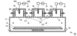
- FIG. 6 shows a schematic longitudinal sectional view of a second embodiment of the plasma processing apparatus according to the present invention.
- the plasma processing apparatus 20 of the present embodiment has the same configuration as that of the plasma processing apparatus 10 of the first embodiment, except that a plurality of plasma generation chambers 22 are provided on the top plate 111 of one plasma processing chamber 11. Have.
- the energy of electrons in the plasma in each plasma generation chamber 22 can be individually and easily adjusted by independently adjusting the position of the plasma control plate 17 in each plasma generation chamber 22. Can be controlled. Thereby, since it can control so that the deposition rate of each part of the board
- the plasma state can be individually changed by introducing different gases in each plasma generation chamber, and film formation with a high degree of freedom can be performed.
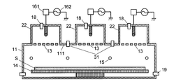
- FIG. 7 shows a schematic longitudinal sectional view of a third embodiment of the plasma processing apparatus according to the present invention.
- the plasma processing apparatus 30 of the present embodiment is the same as the plasma processing apparatus 20 shown in the second embodiment. Is provided.
- the upper exhaust port 31 includes a vacuum pump (exhaust means) (not shown) and an exhaust amount adjusting unit that adjusts the exhaust amount of the vacuum pump.
- vacuum exhaust in the plasma processing chamber 11 is performed through an exhaust port (lower exhaust port) 19 disposed below the substrate S. This is to prevent the processing gas used for film formation from being exhausted more than necessary.
- different exhaust ports (specifically, the upper exhaust port 31) are equally arranged in the plasma processing chamber 11, and the respective exhaust amounts are adjusted by the exhaust amount adjusting unit.
- the time during which the processing gas introduced into the plasma processing chamber 11 exists in the plasma processing chamber is adjusted to be substantially constant.
- a semiconductor film can be formed on the substrate.
- the provision of the upper exhaust port 31 can be suitably used for a plasma processing apparatus having a structure that does not include the plasma control plate 17 shown in FIG.
- a plasma processing apparatus having a structure shown in FIG. 9 can be used.
- a plurality of plasma generation chambers 22 are connected to the plasma processing chamber 11 via partition plates 33.
- the partition plate 33 is provided with a through-hole 331 and a processing gas introduction hole 332 immediately below each plasma generation chamber 22,
- An exhaust hole 333 is provided in a region between the plasma generation chambers 22. This exhaust hole 333 corresponds to the upper exhaust port 31 of the third embodiment.
- the exhaust hole 333 is connected to an exhaust pipe 3331 embedded in the plate material of the partition plate 33, and a process introduced into the plasma processing chamber 11 by a vacuum pump and an exhaust amount adjusting unit (not shown) provided in the exhaust pipe 3331.
- the time during which the gas is present in the plasma processing chamber is adjusted to be substantially constant.
- the present invention is not limited to these embodiments.
- a high-frequency antenna used in a conventional inductively coupled plasma processing apparatus such as a plate-shaped high-frequency antenna or a winding coil is used.
- a plurality of high-frequency antennas may be provided in each plasma generation chamber. It can also be provided outside the plasma generation chamber.
- this invention is not limited to a film forming process. For example, it can also be used for plasma processes that require radical density control, such as an etching process, an ashing process, or a cleaning process.
Landscapes
- Engineering & Computer Science (AREA)
- Physics & Mathematics (AREA)
- Chemical & Material Sciences (AREA)
- Plasma & Fusion (AREA)
- Analytical Chemistry (AREA)
- Electromagnetism (AREA)
- Materials Engineering (AREA)
- Mechanical Engineering (AREA)
- Metallurgy (AREA)
- Organic Chemistry (AREA)
- Chemical Kinetics & Catalysis (AREA)
- Spectroscopy & Molecular Physics (AREA)
- General Chemical & Material Sciences (AREA)
- General Physics & Mathematics (AREA)
- Condensed Matter Physics & Semiconductors (AREA)
- Manufacturing & Machinery (AREA)
- Computer Hardware Design (AREA)
- Microelectronics & Electronic Packaging (AREA)
- Power Engineering (AREA)
- Inorganic Chemistry (AREA)
- Chemical Vapour Deposition (AREA)
- Plasma Technology (AREA)
- Drying Of Semiconductors (AREA)
Abstract
Description
プラズマ生成室と、前記プラズマ生成室内に設けられた高周波アンテナと、プラズマを生成するためのガスを前記プラズマ生成室内に導入するプラズマ生成ガス導入手段と、前記プラズマ生成室と連通するプラズマ処理室と、前記プラズマ処理室内に処理ガスを導入する処理ガス導入手段と、を備えるプラズマ処理装置において、
前記プラズマ生成室内に設けられ、前記高周波アンテナとの距離を変更可能なプラズマ制御板と、
前記プラズマ制御板を移動させるための移動手段と、
を備えることを特徴とする。
この実験装置は、鉛直(以下、「縦」又は「上下」と称す)方向及び水平(以下、「横」と称す)方向に延びる直径150mmの2つの円筒管が互いにクロスした構造を有するステンレス製のクロス管チャンバ51と、クロス管チャンバ51の横方向に延びる円筒管の一方の端部からクロス管チャンバ51内に介挿された、U字形導体から成る高周波アンテナ52と、もう一方の端部からクロス管チャンバ51内に介挿された、プラズマの各種状態を測定するためのラングミュアプローブ53と、高周波アンテナ52の両側の等間隔の位置に配置した縦280mm、横97mm、厚さ6mmの2枚のアルミニウム製平板から成るプラズマ制御板54と、を有する。
まず、プラズマ生成室12内に、プラズマ生成ガス導入口18からプラズマ生成ガスとして水素(H2)ガスを導入すると共に、プラズマ処理室11内に、処理ガス導入口15から処理ガスとしてSiH4ガスを含有する気体を導入する。ここで、プラズマ処理室11内の圧力は1Pa以下とし、プラズマ生成室12内の圧力はプラズマ処理室11内よりも高い2Paとする。このようにプラズマ処理室11とプラズマ生成室12に差圧を設けることで、プラズマ処理室11内に導入された処理ガス(SiH4ガス)が、仕切り板13の貫通孔を通してプラズマ生成室12内に入り込むことを防ぐことができる。
また、上記各実施例では、製膜プロセスについて説明したが、本発明は製膜プロセスには限定されない。例えばエッチングプロセスやアッシングプロセス或いはクリーニングプロセスを始めとするラジカル密度制御が必要なプラズマプロセスにも用いることができる。
11…プラズマ処理室
111…天板
12、22…プラズマ生成室
13、33…仕切り板
131、331…貫通孔
132、332…処理ガス導入孔
1321、3321…処理ガス導入管
133、333…排気孔
1331、3331…排気管
14…基板台
15…処理ガス導入口
16…高周波アンテナ
161、521…インピーダンス整合器
162、522…高周波電源
17、54…プラズマ制御板
171…操作棒
172…移動機構
18…プラズマ生成ガス導入口
19…排気口(下部排気口)
31…上部排気口
51…クロス管チャンバ
52…高周波アンテナ
Claims (12)
- プラズマ生成室と、前記プラズマ生成室内に設けられた高周波アンテナと、プラズマを生成するためのガスを前記プラズマ生成室内に導入するプラズマ生成ガス導入手段と、前記プラズマ生成室と連通するプラズマ処理室と、前記プラズマ処理室内に処理ガスを導入する処理ガス導入手段と、を備えるプラズマ処理装置において、
前記プラズマ生成室内に設けられ、前記高周波アンテナとの距離を変更可能なプラズマ制御板と、
前記プラズマ制御板を移動させるための移動手段と、
を備えることを特徴とするプラズマ処理装置。 - 前記プラズマ生成室が、複数備わっていることを特徴とする請求項1に記載のプラズマ処理装置。
- 前記プラズマ生成室と前記プラズマ処理室の間に差圧を生成する差圧生成手段を備えることを特徴とする請求項1又は2に記載のプラズマ処理装置。
- 前記差圧生成手段が、貫通孔を多数有する板材を前記プラズマ生成室と前記プラズマ処理室の境界に設けたものであることを特徴とする請求項3に記載のプラズマ処理装置。
- 前記板材の前記プラズマ処理室側の面に、前記処理ガスを導入するための処理ガス導入孔が設けられていることを特徴とする請求項4に記載のプラズマ処理装置。
- 前記板材が、前記プラズマ処理室の同一の壁面に一定の間隔をおいて設けられた複数のプラズマ処理室を覆うものであり、該板材の、各プラズマ生成室の間の領域において、プラズマ処理室内の排気を行うための排気手段及び該排気手段の排気量の調整を行うための排気量調整手段が設けられていることを特徴とする請求項4又は5に記載のプラズマ処理装置。
- 前記複数のプラズマ生成室が、前記プラズマ処理室の壁面に一定の間隔をおいて設けられ、これらのプラズマ生成室の間に、プラズマ処理室内の排気を行うための排気手段及び該排気手段の排気量の調整を行うための排気量調整手段が設けられていることを特徴とする請求項2~5のいずれかに記載のプラズマ処理装置。
- プラズマ生成室と、前記プラズマ生成室内に設けられた高周波アンテナと、プラズマを生成するためのガスを前記プラズマ生成室内に導入するプラズマ生成ガス導入手段と、前記プラズマ生成室と連通するプラズマ処理室と、前記プラズマ処理室内に処理ガスを導入する処理ガス導入手段と、を備えるプラズマ処理装置において、
前記プラズマ生成室が、前記プラズマ処理室の壁面に一定の間隔をおいて複数設けられ、
前記複数のプラズマ生成室の間に、プラズマ処理室内の排気を行うための排気手段及び該排気手段の排気量の調整を行うための排気量調整手段が設けられている
ことを特徴とするプラズマ処理装置。 - 前記プラズマ生成室と前記プラズマ処理室の間に差圧を生成する差圧生成手段を備えることを特徴とする請求項8に記載のプラズマ処理装置。
- 前記差圧生成手段が、貫通孔を多数有する板材を前記プラズマ生成室と前記プラズマ処理室の境界に設けたものであることを特徴とする請求項9に記載のプラズマ処理装置。
- 前記板材の前記プラズマ処理室側の面に、前記処理ガスを導入するための処理ガス導入孔が設けられていることを特徴とする請求項10に記載のプラズマ処理装置。
- 前記板材が、前記プラズマ処理室の同一の壁面に設けられた複数のプラズマ処理室を覆うものであることを特徴とする請求項10又は11に記載のプラズマ処理装置。
Priority Applications (5)
| Application Number | Priority Date | Filing Date | Title |
|---|---|---|---|
| CN201180037725.2A CN103155103B (zh) | 2010-08-02 | 2011-08-02 | 等离子体处理装置 |
| KR1020137005321A KR101454132B1 (ko) | 2010-08-02 | 2011-08-02 | 플라스마 처리장치 |
| US13/813,602 US20130192759A1 (en) | 2010-08-02 | 2011-08-02 | Plasma processing device |
| EP11814649.7A EP2602813A1 (en) | 2010-08-02 | 2011-08-02 | Plasma treatment device |
| KR1020147022431A KR101523893B1 (ko) | 2010-08-02 | 2011-08-02 | 플라스마 처리장치 |
Applications Claiming Priority (2)
| Application Number | Priority Date | Filing Date | Title |
|---|---|---|---|
| JP2010-173507 | 2010-08-02 | ||
| JP2010173507A JP5735232B2 (ja) | 2010-08-02 | 2010-08-02 | プラズマ処理装置 |
Publications (1)
| Publication Number | Publication Date |
|---|---|
| WO2012018024A1 true WO2012018024A1 (ja) | 2012-02-09 |
Family
ID=45559521
Family Applications (1)
| Application Number | Title | Priority Date | Filing Date |
|---|---|---|---|
| PCT/JP2011/067698 WO2012018024A1 (ja) | 2010-08-02 | 2011-08-02 | プラズマ処理装置 |
Country Status (7)
| Country | Link |
|---|---|
| US (1) | US20130192759A1 (ja) |
| EP (1) | EP2602813A1 (ja) |
| JP (1) | JP5735232B2 (ja) |
| KR (2) | KR101523893B1 (ja) |
| CN (1) | CN103155103B (ja) |
| TW (1) | TWI515760B (ja) |
| WO (1) | WO2012018024A1 (ja) |
Cited By (1)
| Publication number | Priority date | Publication date | Assignee | Title |
|---|---|---|---|---|
| JP2016072065A (ja) * | 2014-09-30 | 2016-05-09 | 株式会社Screenホールディングス | プラズマ処理装置 |
Families Citing this family (12)
| Publication number | Priority date | Publication date | Assignee | Title |
|---|---|---|---|---|
| US9793126B2 (en) * | 2010-08-04 | 2017-10-17 | Lam Research Corporation | Ion to neutral control for wafer processing with dual plasma source reactor |
| CN103155718B (zh) * | 2010-09-06 | 2016-09-28 | Emd株式会社 | 等离子处理装置 |
| US9245761B2 (en) | 2013-04-05 | 2016-01-26 | Lam Research Corporation | Internal plasma grid for semiconductor fabrication |
| US9147581B2 (en) | 2013-07-11 | 2015-09-29 | Lam Research Corporation | Dual chamber plasma etcher with ion accelerator |
| JP2015074792A (ja) * | 2013-10-07 | 2015-04-20 | 株式会社Screenホールディングス | プラズマcvd装置 |
| GB2531233A (en) * | 2014-02-27 | 2016-04-20 | C Tech Innovation Ltd | Plasma enhanced catalytic conversion method and apparatus |
| JP6431303B2 (ja) * | 2014-07-03 | 2018-11-28 | 株式会社Screenホールディングス | エッチング装置およびエッチング方法 |
| JP6863608B2 (ja) * | 2016-06-24 | 2021-04-21 | 株式会社イー・エム・ディー | プラズマ源及びプラズマ処理装置 |
| CN108987228B (zh) * | 2017-06-02 | 2024-05-17 | 北京北方华创微电子装备有限公司 | 用于处理工件的等离子体反应装置 |
| US20200347499A1 (en) * | 2019-05-01 | 2020-11-05 | Applied Materials, Inc. | Large-area high-density plasma processing chamber for flat panel displays |
| JP2021077451A (ja) * | 2019-11-05 | 2021-05-20 | 東京エレクトロン株式会社 | プラズマ処理装置およびプラズマ処理方法 |
| JP6809745B1 (ja) * | 2020-08-03 | 2021-01-06 | 株式会社ニッシン | プラズマ処理装置 |
Citations (3)
| Publication number | Priority date | Publication date | Assignee | Title |
|---|---|---|---|---|
| JP2003188154A (ja) * | 2001-12-21 | 2003-07-04 | Sharp Corp | プラズマプロセス装置およびプラズマ制御方法 |
| JP2003332307A (ja) * | 2002-05-08 | 2003-11-21 | Tokyo Electron Ltd | プラズマ処理装置 |
| JP2007035411A (ja) * | 2005-07-26 | 2007-02-08 | Hitachi High-Technologies Corp | プラズマ処理装置 |
Family Cites Families (17)
| Publication number | Priority date | Publication date | Assignee | Title |
|---|---|---|---|---|
| JP3132599B2 (ja) * | 1992-08-05 | 2001-02-05 | 株式会社日立製作所 | マイクロ波プラズマ処理装置 |
| JPH07142463A (ja) * | 1993-11-22 | 1995-06-02 | Nec Corp | 半導体装置の製造方法と製造装置 |
| JPH08222399A (ja) * | 1994-12-14 | 1996-08-30 | Adtec:Kk | 高周波プラズマ発生装置 |
| US5683548A (en) * | 1996-02-22 | 1997-11-04 | Motorola, Inc. | Inductively coupled plasma reactor and process |
| DE19841777C1 (de) * | 1998-09-12 | 2000-01-05 | Fraunhofer Ges Forschung | Vorrichtung zur plasmatechnischen Abscheidung von polykristallinem Diamant |
| JP3514186B2 (ja) * | 1999-09-16 | 2004-03-31 | 日新電機株式会社 | 薄膜形成方法及び装置 |
| JP2003529926A (ja) * | 2000-03-30 | 2003-10-07 | 東京エレクトロン株式会社 | プラズマ処理システム内への調整可能なガス注入のための方法及び装置 |
| JP4371543B2 (ja) * | 2000-06-29 | 2009-11-25 | 日本電気株式会社 | リモートプラズマcvd装置及び膜形成方法 |
| US20030024900A1 (en) * | 2001-07-24 | 2003-02-06 | Tokyo Electron Limited | Variable aspect ratio plasma source |
| JP5162108B2 (ja) * | 2005-10-28 | 2013-03-13 | 日新電機株式会社 | プラズマ生成方法及び装置並びにプラズマ処理装置 |
| JP5082411B2 (ja) * | 2006-12-01 | 2012-11-28 | 東京エレクトロン株式会社 | 成膜方法 |
| US8528498B2 (en) * | 2007-06-29 | 2013-09-10 | Lam Research Corporation | Integrated steerability array arrangement for minimizing non-uniformity |
| JP2009123934A (ja) * | 2007-11-15 | 2009-06-04 | Tokyo Electron Ltd | プラズマ処理装置 |
| JP5227245B2 (ja) * | 2009-04-28 | 2013-07-03 | 東京エレクトロン株式会社 | プラズマ処理装置 |
| US8900402B2 (en) * | 2011-05-10 | 2014-12-02 | Lam Research Corporation | Semiconductor processing system having multiple decoupled plasma sources |
| US8900403B2 (en) * | 2011-05-10 | 2014-12-02 | Lam Research Corporation | Semiconductor processing system having multiple decoupled plasma sources |
| KR20130072941A (ko) * | 2011-12-22 | 2013-07-02 | 삼성전자주식회사 | 플라즈마 식각 장치 |
-
2010
- 2010-08-02 JP JP2010173507A patent/JP5735232B2/ja active Active
-
2011
- 2011-08-02 TW TW100127333A patent/TWI515760B/zh active
- 2011-08-02 US US13/813,602 patent/US20130192759A1/en not_active Abandoned
- 2011-08-02 WO PCT/JP2011/067698 patent/WO2012018024A1/ja active Application Filing
- 2011-08-02 EP EP11814649.7A patent/EP2602813A1/en not_active Withdrawn
- 2011-08-02 CN CN201180037725.2A patent/CN103155103B/zh active Active
- 2011-08-02 KR KR1020147022431A patent/KR101523893B1/ko active IP Right Grant
- 2011-08-02 KR KR1020137005321A patent/KR101454132B1/ko active IP Right Grant
Patent Citations (3)
| Publication number | Priority date | Publication date | Assignee | Title |
|---|---|---|---|---|
| JP2003188154A (ja) * | 2001-12-21 | 2003-07-04 | Sharp Corp | プラズマプロセス装置およびプラズマ制御方法 |
| JP2003332307A (ja) * | 2002-05-08 | 2003-11-21 | Tokyo Electron Ltd | プラズマ処理装置 |
| JP2007035411A (ja) * | 2005-07-26 | 2007-02-08 | Hitachi High-Technologies Corp | プラズマ処理装置 |
Cited By (1)
| Publication number | Priority date | Publication date | Assignee | Title |
|---|---|---|---|---|
| JP2016072065A (ja) * | 2014-09-30 | 2016-05-09 | 株式会社Screenホールディングス | プラズマ処理装置 |
Also Published As
| Publication number | Publication date |
|---|---|
| TWI515760B (zh) | 2016-01-01 |
| US20130192759A1 (en) | 2013-08-01 |
| CN103155103B (zh) | 2016-06-08 |
| KR101523893B1 (ko) | 2015-05-28 |
| KR20130062982A (ko) | 2013-06-13 |
| TW201234407A (en) | 2012-08-16 |
| KR20140108331A (ko) | 2014-09-05 |
| JP5735232B2 (ja) | 2015-06-17 |
| CN103155103A (zh) | 2013-06-12 |
| EP2602813A1 (en) | 2013-06-12 |
| JP2012033803A (ja) | 2012-02-16 |
| KR101454132B1 (ko) | 2014-10-22 |
Similar Documents
| Publication | Publication Date | Title |
|---|---|---|
| JP5735232B2 (ja) | プラズマ処理装置 | |
| JP4273932B2 (ja) | 表面波励起プラズマcvd装置 | |
| JP4540742B2 (ja) | 原子層成長装置および薄膜形成方法 | |
| JP6410622B2 (ja) | プラズマ処理装置及び成膜方法 | |
| US7392759B2 (en) | Remote plasma apparatus for processing substrate with two types of gases | |
| KR102418243B1 (ko) | 플라즈마 처리 장치 및 플라즈마 처리 방법 | |
| JP2009191311A (ja) | 原子層成長装置 | |
| JP4426632B2 (ja) | プラズマ処理装置 | |
| JP2009206312A (ja) | 成膜方法および成膜装置 | |
| JP4575998B2 (ja) | 薄膜形成装置および薄膜形成方法 | |
| JP4273983B2 (ja) | 表面波励起プラズマcvd装置 | |
| JP2022093741A (ja) | プラズマcvd装置 | |
| JP2004296868A (ja) | プラズマ処理装置及び処理方法 | |
| JP2007184259A (ja) | プラズマ生成装置およびプラズマ処理製造方法 | |
| JP2022168101A (ja) | プラズマ支援ald装置 | |
| JP2022080926A (ja) | 成膜方法及び成膜装置 | |
| JP5078656B2 (ja) | 原子層成長装置 | |
| JP2013207248A (ja) | プラズマ形成方法及びプラズマ形成装置 | |
| JP2016091617A (ja) | プラズマ処理装置 | |
| JP2007273865A (ja) | プラズマエッチング装置 |
Legal Events
| Date | Code | Title | Description |
|---|---|---|---|
| WWE | Wipo information: entry into national phase |
Ref document number: 201180037725.2 Country of ref document: CN |
|
| 121 | Ep: the epo has been informed by wipo that ep was designated in this application |
Ref document number: 11814649 Country of ref document: EP Kind code of ref document: A1 |
|
| NENP | Non-entry into the national phase |
Ref country code: DE |
|
| WWE | Wipo information: entry into national phase |
Ref document number: 2011814649 Country of ref document: EP |
|
| ENP | Entry into the national phase |
Ref document number: 20137005321 Country of ref document: KR Kind code of ref document: A |
|
| WWE | Wipo information: entry into national phase |
Ref document number: 13813602 Country of ref document: US |