WO2012017494A1 - 有機el表示パネル、表示装置、及び有機el表示パネルの製造方法 - Google Patents
有機el表示パネル、表示装置、及び有機el表示パネルの製造方法 Download PDFInfo
- Publication number
- WO2012017494A1 WO2012017494A1 PCT/JP2010/004984 JP2010004984W WO2012017494A1 WO 2012017494 A1 WO2012017494 A1 WO 2012017494A1 JP 2010004984 W JP2010004984 W JP 2010004984W WO 2012017494 A1 WO2012017494 A1 WO 2012017494A1
- Authority
- WO
- WIPO (PCT)
- Prior art keywords
- functional layer
- organic functional
- color
- electrode plate
- contact hole
- Prior art date
- Legal status (The legal status is an assumption and is not a legal conclusion. Google has not performed a legal analysis and makes no representation as to the accuracy of the status listed.)
- Ceased
Links
Images



Classifications
-
- H—ELECTRICITY
- H10—SEMICONDUCTOR DEVICES; ELECTRIC SOLID-STATE DEVICES NOT OTHERWISE PROVIDED FOR
- H10K—ORGANIC ELECTRIC SOLID-STATE DEVICES
- H10K59/00—Integrated devices, or assemblies of multiple devices, comprising at least one organic light-emitting element covered by group H10K50/00
- H10K59/30—Devices specially adapted for multicolour light emission
- H10K59/35—Devices specially adapted for multicolour light emission comprising red-green-blue [RGB] subpixels
- H10K59/352—Devices specially adapted for multicolour light emission comprising red-green-blue [RGB] subpixels the areas of the RGB subpixels being different
-
- H—ELECTRICITY
- H10—SEMICONDUCTOR DEVICES; ELECTRIC SOLID-STATE DEVICES NOT OTHERWISE PROVIDED FOR
- H10K—ORGANIC ELECTRIC SOLID-STATE DEVICES
- H10K10/00—Organic devices specially adapted for rectifying, amplifying, oscillating or switching; Organic capacitors or resistors having potential barriers
- H10K10/40—Organic transistors
- H10K10/46—Field-effect transistors, e.g. organic thin-film transistors [OTFT]
-
- H—ELECTRICITY
- H10—SEMICONDUCTOR DEVICES; ELECTRIC SOLID-STATE DEVICES NOT OTHERWISE PROVIDED FOR
- H10K—ORGANIC ELECTRIC SOLID-STATE DEVICES
- H10K50/00—Organic light-emitting devices
- H10K50/30—Organic light-emitting transistors
-
- H—ELECTRICITY
- H10—SEMICONDUCTOR DEVICES; ELECTRIC SOLID-STATE DEVICES NOT OTHERWISE PROVIDED FOR
- H10K—ORGANIC ELECTRIC SOLID-STATE DEVICES
- H10K50/00—Organic light-emitting devices
- H10K50/80—Constructional details
- H10K50/805—Electrodes
- H10K50/81—Anodes
- H10K50/814—Anodes combined with auxiliary electrodes, e.g. ITO layer combined with metal lines
-
- H—ELECTRICITY
- H10—SEMICONDUCTOR DEVICES; ELECTRIC SOLID-STATE DEVICES NOT OTHERWISE PROVIDED FOR
- H10K—ORGANIC ELECTRIC SOLID-STATE DEVICES
- H10K59/00—Integrated devices, or assemblies of multiple devices, comprising at least one organic light-emitting element covered by group H10K50/00
- H10K59/10—OLED displays
- H10K59/12—Active-matrix OLED [AMOLED] displays
- H10K59/122—Pixel-defining structures or layers, e.g. banks
-
- H—ELECTRICITY
- H10—SEMICONDUCTOR DEVICES; ELECTRIC SOLID-STATE DEVICES NOT OTHERWISE PROVIDED FOR
- H10K—ORGANIC ELECTRIC SOLID-STATE DEVICES
- H10K59/00—Integrated devices, or assemblies of multiple devices, comprising at least one organic light-emitting element covered by group H10K50/00
- H10K59/10—OLED displays
- H10K59/12—Active-matrix OLED [AMOLED] displays
- H10K59/124—Insulating layers formed between TFT elements and OLED elements
-
- H—ELECTRICITY
- H10—SEMICONDUCTOR DEVICES; ELECTRIC SOLID-STATE DEVICES NOT OTHERWISE PROVIDED FOR
- H10K—ORGANIC ELECTRIC SOLID-STATE DEVICES
- H10K59/00—Integrated devices, or assemblies of multiple devices, comprising at least one organic light-emitting element covered by group H10K50/00
- H10K59/80—Constructional details
- H10K59/805—Electrodes
- H10K59/8051—Anodes
- H10K59/80516—Anodes combined with auxiliary electrodes, e.g. ITO layer combined with metal lines
-
- H—ELECTRICITY
- H10—SEMICONDUCTOR DEVICES; ELECTRIC SOLID-STATE DEVICES NOT OTHERWISE PROVIDED FOR
- H10K—ORGANIC ELECTRIC SOLID-STATE DEVICES
- H10K71/00—Manufacture or treatment specially adapted for the organic devices covered by this subclass
- H10K71/10—Deposition of organic active material
- H10K71/12—Deposition of organic active material using liquid deposition, e.g. spin coating
- H10K71/13—Deposition of organic active material using liquid deposition, e.g. spin coating using printing techniques, e.g. ink-jet printing or screen printing
- H10K71/135—Deposition of organic active material using liquid deposition, e.g. spin coating using printing techniques, e.g. ink-jet printing or screen printing using ink-jet printing
-
- H—ELECTRICITY
- H10—SEMICONDUCTOR DEVICES; ELECTRIC SOLID-STATE DEVICES NOT OTHERWISE PROVIDED FOR
- H10K—ORGANIC ELECTRIC SOLID-STATE DEVICES
- H10K2102/00—Constructional details relating to the organic devices covered by this subclass
- H10K2102/301—Details of OLEDs
- H10K2102/302—Details of OLEDs of OLED structures
- H10K2102/3023—Direction of light emission
- H10K2102/3026—Top emission
-
- H—ELECTRICITY
- H10—SEMICONDUCTOR DEVICES; ELECTRIC SOLID-STATE DEVICES NOT OTHERWISE PROVIDED FOR
- H10K—ORGANIC ELECTRIC SOLID-STATE DEVICES
- H10K2102/00—Constructional details relating to the organic devices covered by this subclass
- H10K2102/301—Details of OLEDs
- H10K2102/351—Thickness
Definitions
- the present invention relates to an organic EL display panel in which organic electroluminescent elements (hereinafter referred to as “organic EL elements”) are arranged, a display device, and a method for manufacturing the organic EL display panel.
- organic EL elements organic electroluminescent elements
- an organic EL display panel in which a plurality of organic EL elements are arranged on a substrate in a matrix direction is used as a light-emitting display panel in a small electronic device or a small display device.
- the organic EL element has a basic structure in which a light emitting layer containing an organic light emitting material is formed between a pair of electrodes of an anode and a cathode. When a voltage is applied between a pair of electrodes, the organic EL element emits light in association with recombination of holes injected from the anode into the light emitting layer and electrons injected from the cathode into the light emitting layer.
- This organic EL display panel has high visibility because each organic EL element emits light by itself.
- a light emitting layer is generally partitioned for each organic EL element by a partition (bank) made of an insulating material, and a region where the light emitting layer is formed is defined by the partition. Further, an intermediate layer such as a hole injection layer, a hole transport layer, and a hole injection / transport layer is interposed between the anode and the light emitting layer as necessary. Further, an electron injection layer, an electron transport layer, or an electron injection / transport layer is interposed between the cathode and the light emitting layer as necessary.
- organic EL elements form RGB (red, green, and blue) subpixels, and adjacent RGB subpixels are combined to form one pixel.
- a partition wall for partitioning adjacent organic EL elements is formed on the substrate, and a high molecular material or a low molecular material having good thin film formability is formed.
- Many wet methods are used in which an ink containing ink is applied by inkjet or the like. According to this wet method, an intermediate layer and a light emitting layer can be formed relatively easily even in a large panel.
- the inkjet head is moved in one of the matrix directions above the substrate to be coated, and an intermediate layer and light emission are formed in a region partitioned by a partition on the substrate.
- Ink is applied by discharging droplets of a solution (hereinafter simply referred to as “ink”) containing an organic material and a solvent for forming a layer or the like from a nozzle (see Patent Document 1).
- the film thickness of the intermediate layer suitable for increasing the luminous efficiency of each organic EL element depends on the wavelength of the luminescent color.
- a top emission type organic EL element light emitted from the light emitting layer to the substrate side is reflected once by the electrode on the substrate side, and then reflected through the light emitting layer and emitted from the light emitting layer. It is desirable that the optical path length is set so that the light emitted directly upward (on the opposite side of the substrate) from each other strengthens.
- the optimum optical path length (resonance condition) in the organic EL element differs depending on the wavelength of red light, green light, and blue light. Therefore, in each color subpixel, the intermediate layer is matched to the wavelength of the emission color. It is desirable to finely adjust the difference in film thickness in order to increase the light emission efficiency.
- the ink including the material of the intermediate layer is common to all colors, and the amount of ink for forming the intermediate layer supplied to each subpixel is made constant.
- the number of ink droplets ejected to the area where the organic EL elements of each color are formed is the same, and the volume per ink droplet ejected from the nozzle is the same. While doing.
- the ink jet method it may be possible to adjust the film thickness of the intermediate layer by changing the number of ink droplets dropped for each subpixel color. Since it can be changed only in units of droplets, it is practically difficult to finely adjust the thickness of the intermediate layer for each subpixel color.
- the appropriate film thickness for obtaining desired luminance and chromaticity differs for each color, so that the film thickness difference between the light-emitting layers corresponding to different colors can be finely adjusted, or the intermediate layer Similarly, it is required to finely adjust the film thickness difference in order to make the optical path length suitable for the wavelength of the emission color.
- the present invention has been made in view of such problems, and in an organic EL display panel, an intermediate layer or a light emitting layer is formed by a wet method, and a difference in film thickness of an intermediate layer or the like between different emission colors can be easily achieved. For example, it is intended to improve the light emission efficiency, the light emission color, and the like.
- a TFT layer, an interlayer insulating film provided above the TFT layer, and the interlayer insulating film are formed in a line shape.
- a second electrode plate group including a color electrode plate, a first partition formed along one long side portion of the first electrode plate group, and the other long side portion of the first electrode plate group; A second barrier rib formed between one long side portion of the second electrode plate group, a third barrier rib formed along the other long side portion of the second electrode plate group, A first organic functional layer formed between the first barrier rib and the second barrier rib above the first electrode plate group; and the second barrier rib A second organic functional layer formed above the second electrode plate group between the third barrier ribs, a counter electrode provided above the first organic functional layer and the second organic functional layer,
- the interlayer insulating film includes a first contact hole connecting each of the first color electrode plates and the TFT layer, and each of the second color electrode plates and the TFT layer.
- a second contact hole to be connected is provided, and each of the first color electrode plates has a first recess portion that is recessed along the shape of the first contact hole, and the second color electrode plate Each of which has a second recessed portion that is recessed along the shape of the second contact hole, and the first contact hole and the second color electrode plate corresponding to the first color electrode plate.
- At least one of the second contact holes corresponding to the shape that narrows stepwise The volume of the first contact hole is larger than the volume of the second contact hole, and the volume of the first organic functional layer corresponding to the region on the electrode plate for the first color is the second
- the volume of the first organic functional layer corresponds to the first contact hole, which is the same or the same value as the volume of the second organic functional layer corresponding to the region on the color electrode plate.
- the structure is thinner than the film thickness of the second organic functional layer formed in the region on the electrode plate for the second color other than the second depression. It has been adopted.
- a display device includes the organic EL display panel.
- a first step of preparing a substrate, a second step of forming a TFT layer on the substrate, and an interlayer insulating film on the TFT layer are formed.
- a second partition is formed between the other long side portion of the first electrode plate group and one long side portion of the second electrode plate group, and along the other long side portion of the second electrode plate group
- a first contact hole for connecting each of the electrode plates and the TFT layer and a second contact hole for connecting each of the second color electrode plates and the TFT layer are formed. At least one of the first contact hole corresponding to the plate and the second contact hole corresponding to the electrode plate for the second color is formed in a gradually narrowing shape, and the first contact hole is the second contact hole.
- each of the first color electrode plates is formed with a first recess along the shape of the first contact hole, and each of the second color electrode plates has the first color.
- a second depression is formed along the shape of the two contact holes.
- the volume of the first organic functional layer corresponding to the region on the electrode plate for color is the same or the same neighborhood value as the volume of the second organic functional layer corresponding to the region on the electrode plate for second color
- the thickness of the first organic functional layer is a second thickness corresponding to the second contact hole in the amount of the first organic functional layer entering the first recess corresponding to the first contact hole.
- the film of the second organic functional layer formed in the region on the electrode plate for the second color other than the second recess in the region on the electrode plate for the first color other than the first recess is adopted.
- the volume (volume) of the first contact hole can be easily achieved by forming at least one of the first contact hole and the second contact hole in a gradually narrowing shape. Can be made larger than the volume (volume) of the second contact hole.
- the volume of the first dent portion is larger than the volume of the second dent portion, and in the formation of the organic functional layer by the wet method, for example, the first organic functional layer and the second organic function formed above the electrode plate
- the amount of the first organic functional layer that enters the first depression can be larger than the amount of the second organic functional layer that enters the second depression.
- the region other than the first depression of the electrode plate for the first color is set to a region other than the second depression of the electrode plate for the second color.
- the thickness of the corresponding second organic functional layer (hereinafter simply referred to as the thickness of the second organic functional layer) can be made thinner.
- the difference between the volume of the first depression and the volume of the second depression can be adjusted in a unit smaller than the volume per droplet of ink ejected from the nozzle in the ink jet coating method. Therefore, the difference between the film thickness of the first organic functional layer and the film thickness of the second organic functional layer can be easily adjusted by finely adjusting the difference between the volume of the first hollow part and the volume of the second hollow part. Can be adjusted.
- the resonance condition of light in the organic EL element can be optimized for each color, and a display panel having excellent light emission efficiency can be easily obtained.
- the film thickness can be adjusted.
- the above-described organic EL display panel can be produced.
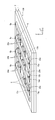
- FIG. 2 is a perspective view showing a schematic configuration of a display panel 100.
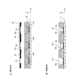
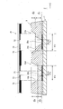
- FIG. (A) is a plan view showing a schematic configuration of the display panel 100
- (b) is a cross-sectional view cut along the line AA ′ in (a)
- (c) is cut along the line BB ′ in (a).
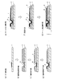
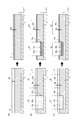
- FIG. 4 is a diagram for explaining a method of manufacturing the display panel 100.
- FIG. 4 is a diagram for explaining a process of forming an interlayer insulating film of the display panel 100.
- FIG. 6 is a schematic diagram for explaining the relationship between the volume of a hollow portion 15 and the film thickness of a hole transport layer 9.
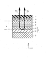
- FIG. 4 is a diagram for explaining an upper area of a contact hole 13. 4 is a schematic diagram for explaining how light travels in the organic EL element 20.
- FIG. 10 is a schematic diagram showing the shape of a contact hole 13d according to Modification 1.
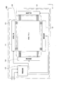
- FIG. It is a figure which shows the whole structure of the display apparatus 200 which concerns on embodiment. It is an external appearance which shows an example of the television system using the display apparatus 200.
- FIG. 6 is a schematic diagram for explaining the relationship between the volume of a hollow portion 15 and the film thickness of a hole transport layer 9.
- FIG. 4 is a diagram for explaining an upper area of a contact hole 13. 4 is a schematic diagram for explaining how light travels in the organic EL element 20.
- FIG. 10 is a schematic diagram showing the shape of a contact hole 13d according to Modification 1.
- FIG. It is a figure which shows the whole structure of
- a TFT layer In the organic EL display panel according to an aspect of the present invention, a TFT layer, an interlayer insulating film provided above the TFT layer, and a plurality of first electrodes formed on the interlayer insulating film and arranged in a line.
- a first electrode plate group including a color electrode plate; and a plurality of second color electrode plates formed on the interlayer insulating film adjacent to the first electrode plate group and arranged in a line.
- a second electrode plate group ; a first partition formed along one long side portion of the first electrode plate group; the other long side portion of the first electrode plate group; and the second electrode plate group.
- a second barrier rib formed between the first long side portion, a third barrier rib formed along the other long side portion of the second electrode plate group, the first barrier rib, and the second barrier rib.
- the interlayer insulation The film has a first contact hole that connects each of the first color electrode plates and the TFT layer, and a second contact hole that connects each of the second color electrode plates and the TFT layer.
- Each of the first color electrode plates has a first recess that is recessed along the shape of the first contact hole, and each of the second color electrode plates has the second color.
- the first contact hole corresponding to the first color electrode plate and the second contact hole corresponding to the second color electrode plate have a second recess portion that is recessed along the shape of the contact hole. At least one of them has a shape that narrows in a stepwise manner.
- the volume of the tact hole is larger than the volume of the second contact hole, and the volume of the first organic functional layer corresponding to the region on the electrode plate for the first color is on the electrode plate for the second color.
- the volume of the first organic functional layer is within the range of the same or the same value as the volume of the second organic functional layer corresponding to the region, and the thickness of the first organic functional layer enters the first depression corresponding to the first contact hole. Since the amount of the first organic functional layer is larger than the amount of the second organic functional layer entering the second depression corresponding to the second contact hole, the electrode for the first color other than the first depression In the region on the plate, a configuration is adopted in which the thickness is smaller than the thickness of the second organic functional layer formed in the region on the electrode plate for the second color other than the second depression.
- the volume (volume) of the first contact hole can be easily achieved by forming at least one of the first contact hole and the second contact hole in a gradually narrowing shape. Can be made larger than the volume (volume) of the second contact hole.
- the volume of the first dent portion is larger than the volume of the second dent portion, and in the formation of the organic functional layer by the wet method, for example, the first organic functional layer and the second organic function formed above the electrode plate
- the amount of the first organic functional layer that enters the first depression can be larger than the amount of the second organic functional layer that enters the second depression.
- the region other than the first depression of the electrode plate for the first color is set to a region other than the second depression of the electrode plate for the second color.
- the thickness of the corresponding second organic functional layer (hereinafter simply referred to as the thickness of the second organic functional layer) can be made thinner.
- the difference between the volume of the first depression and the volume of the second depression can be adjusted in a unit smaller than the volume per droplet of ink ejected from the nozzle in the ink jet coating method. Therefore, the difference between the film thickness of the first organic functional layer and the film thickness of the second organic functional layer can be easily adjusted by finely adjusting the difference between the volume of the first hollow part and the volume of the second hollow part. Can be adjusted.
- the resonance condition of light in the organic EL element can be optimized for each color, and a display panel having excellent light emission efficiency can be easily obtained.
- the film thickness can be adjusted.
- the fact that the resonance condition of light in the organic EL element is appropriate for each color means that, for example, the same manufacturing conditions as the organic EL display panel of this aspect (dimension of organic EL element, ink application amount) Etc.), when the organic EL display panel is manufactured with the same volume of the first and second contact holes, the luminous efficiency of both the first and second color organic EL elements is improved. Although it is impossible to make them compatible, it means a state where both the first and second contact holes have different volumes.
- the volumes of the first and second contact holes are the same. If the volume of the first contact hole of the organic EL display panel of this embodiment is reduced to be the same as the volume of the second contact hole, the luminous efficiency of the organic EL element for the first color is reduced, If the volume of the second contact hole is increased to be the same as the volume of the first contact hole, the light emission efficiency of the organic EL element for the second color is lowered.
- optimization of luminescent color is performed by improving the color purity of each luminescent color, for example.
- the volume of the first contact hole may be read as the volume of the first depression, and the volume of the second contact hole may be read as the volume of the second depression.
- the shape of the contact hole that becomes narrower in stages is formed, for example, by exposing and developing an interlayer insulating film in which the contact hole is formed using a halftone mask.
- the number of stepped contact holes and the width and depth of each step can be arbitrarily formed. Further, the step may be formed on a part of the inner periphery of the contact hole or may be formed over the entire periphery.
- the organic functional layer film can be finely adjusted.
- the volume of the first organic functional layer corresponding to the region on the electrode plate for the first color is the same as the volume of the second organic functional layer corresponding to the region on the electrode plate for each second color or “Within the same neighborhood value range” means that the volume of the first organic functional layer and the volume of the second organic functional layer are substantially the same (within the error range), and numerically the first organic functional layer.
- the difference between the volume of the second organic functional layer and the volume of the second organic functional layer is within 10% of the volume of the first organic functional layer.
- the difference between the volume of the first depression and the volume of the second depression may be larger than the volume of one ink drop (for example, 1.5 drops).
- the difference between the volume of the first organic functional layer and the volume of the second organic functional layer is the difference between the volume of the first organic functional layer deposited in the first depression and the second organic functional layer deposited in the second depression. It is desirable that the volume is less than the volume obtained by subtracting the volume.
- the “region on the electrode plate for the first color other than the first recess portion” means, for example, that the first recess portion is formed in the region on the electrode plate for the first color in plan view.
- a flat region excluding the region (which may include a region around the first depression). Specifically, for example, it is a portion located in the light emitting region in plan view. The same applies to the region on the electrode plate for the second color.
- the upper direction means the upper side in the stacking direction of the organic functional layer and the like, and is the direction away from the TFT layer.
- the organic functional layer film can be finely adjusted.
- the organic EL display panel according to an aspect of the present invention includes an upper area of the first contact hole corresponding to the first color electrode plate and an upper area of the second contact hole corresponding to the second color electrode plate.
- a configuration in which the area is within the range of the same or the same neighborhood value can be employed.
- the first contact hole, the second contact hole By providing a step in at least one of the first contact hole, the volume of the first contact hole can be made larger than the volume of the second contact hole. Specifically, for example, by providing a step in the second contact hole and reducing the volume below the step surface, the volume of the second contact hole can be made smaller than that of the first contact hole. As a result, the difference between the film thickness of the first organic functional layer and the film thickness of the second organic functional layer can be finely adjusted.
- the opening areas of the first and second recesses are also substantially the same, and the ease of entering the applied ink into the recesses is approximately equal. can do.
- the upper area is, for example, the opening area of a contact hole opened on the upper surface of the interlayer insulating film, or the opening when the upper part of the contact hole is cut by a cross section perpendicular to the stacking direction of the organic functional layer or the like. It can be an area.
- the upper portion of the contact hole can be, for example, any portion between the uppermost portion of the peripheral portion of the contact hole and a position lowered by 15% of the depth dimension of the contact hole.
- “within the range of the same or the same neighboring value” means that the upper area of the first contact hole and the upper area of the second contact hole are substantially the same (within the error range). It means that the difference between the top area of the first contact hole and the top area of the second contact hole is within 10% of the top area of the first contact hole.
- the upper area of the contact hole is within a range of 10% from the highest position of the peripheral edge of the contact hole in the interlayer insulating film, or a value in the vicinity of 10%. It is possible to adopt a configuration in which the area is a circle defined by the diameter of the contact hole at the position lowered to the point.
- the planar shape of the contact hole is circular, and the upper area is defined by the diameter of the contact hole at a position descending around 10% of the depth of the contact hole from the highest position of the peripheral edge of the contact hole. It is. As a result, even when there is a variation in shape or height at the highest position of the periphery of the contact hole and in the vicinity thereof, the influence can be reduced.
- the range of the vicinity value of 10% can be set to a value within the range of 9% or more and 11% or less, for example.
- the first depression corresponding to the first contact hole is covered with a first pixel restriction layer, and the first organic layer is disposed above the first pixel restriction layer.
- a functional layer is formed, the second depression corresponding to the second contact hole is covered with a second pixel regulating layer, and a second organic functional layer is formed above the second pixel regulating layer;
- the depression and the organic functional layer can be electrically insulated by covering the depression with the pixel regulation layer having insulation.
- the light emitting layer from emitting light with a luminance different from that around the depression due to local current concentration above the opening edge of the depression.
- Each of the first pixel restricting layer and the second pixel restricting layer is, for example, an SiO 2 (silicon oxide) film, or an oxide (including nitride) such as a SiN (silicon nitride) film or a SiON (silicon oxynitride) film. It is formed. Since the oxide such as the SiO film or the SiN film has good wettability with each of the first organic functional layer and the second organic functional layer, the ink including the organic functional layer directly on the pixel regulating layer is directly applied. When applied, the penetration of the first organic functional layer into the first depression and the penetration of the second organic functional layer into the second depression become good.
- the first organic functional layer is continuously applied above the first electrode plate group by applying a predetermined volume of droplets by an ink jet coating method.
- the second organic functional layer is applied to the second electrode plate group by applying droplets having a volume within the range of the same or the same value as the predetermined volume by an ink jet coating method.
- the volume of the first organic functional layer corresponding to the region on the first color electrode plate corresponds to the second color corresponding to the region on the second color electrode plate.
- a configuration in which the volume of the organic functional layer is the same as or within the same range of neighboring values can be employed.
- the volume of droplets dropped by the ink jet coating method is substantially the same in the formation of the first organic functional layer and the formation of the second organic functional layer (for example, a volume difference). Is within an error range of 10% or less). Further, the volume of the first organic functional layer is within the range of the same value as or the same as the volume of the second organic functional layer (for example, within the error range where the volume difference is within 10%), The number of droplets dropped on the same is the same.
- the first organic corresponding to the portion other than the first depression of the electrode plate for the first color since the volume of the first contact hole is larger than the volume of the second contact hole, the first organic corresponding to the portion other than the first depression of the electrode plate for the first color.
- the film thickness of the functional layer can be made thinner than that of the second organic functional layer corresponding to the portion other than the second depression of the electrode plate for the second color.
- the manufacturing apparatus or the manufacturing process is simplified, and the volume of the first contact hole is made larger than that of the second contact hole.
- the film thickness of a 1st organic functional layer can be made thinner than a 2nd organic functional layer. That is, the film thickness difference between the organic functional layers corresponding to different colors can be finely adjusted.
- each organic material is adjusted by adjusting the number of shots of the ink jet device (for example, the number of ink drops per subpixel) for each color such as RGB. Since the thickness of the functional layer was adjusted, it was difficult to finely adjust the thickness of the organic functional layer. For example, in the case where 10 drops of organic ink droplets constituting the organic functional layer are dropped on the region corresponding to the electrode plate for the first color, the film thickness is about 1. It becomes 1 time (about 10% increase). That is, in this case, the ink-jet apparatus cannot perform film thickness control at about 10% or less. Therefore, the film thickness difference between the organic functional layers corresponding to different colors cannot be finely adjusted.
- the organic functional layer is an intermediate layer, printing is performed using the same material for each color such as RGB. At this time, in order to adjust the film thickness difference between the organic functional layers corresponding to different colors, it is necessary to control the number of shots for each of the RGB nozzles of the inkjet apparatus, which complicates the apparatus.
- the volume of the first organic functional layer and the volume of the second organic functional layer are substantially the same.
- the volume difference between the contact holes can be set to, for example, 1.5 drops of ink, and the difference in film thickness of the organic functional layer can be finely adjusted even when the number of shots of each color is the same. That is, in this aspect, even when the amount of dropping by the ink jet apparatus when forming the organic functional layer film is the same for each color of RGB, the film thickness can be arbitrarily finely adjusted according to each light emission color.
- the volume of the first organic functional layer corresponding to the region on the electrode plate for the first color is equal to the volume of the second organic functional layer corresponding to the region on the electrode plate for the second color.
- the film thickness of the organic functional layer can be finely adjusted by adjusting the volume of the recess while keeping the same or the same range of neighboring values.
- the difference between the film thickness of the first organic functional layer and the film thickness of the second organic functional layer is determined by the ink jet coating method.
- the number of droplets applied to each electrode plate for the first color is larger than the film thickness of the first organic functional layer formed by increasing n droplets, and the droplets It is possible to adopt a configuration in which the number is smaller than the film thickness of the first organic functional layer formed by increasing n + 1 drops.
- the film thickness of the first organic functional layer corresponding to a portion other than the first depression portion of the electrode plate for the first color and the portion other than the second depression portion of the electrode plate for the second color.
- the difference from the film thickness of the second organic functional layer can be finely adjusted to be smaller than the film thickness formed by one droplet, which is the minimum unit of droplets dropped from the nozzle of the inkjet device (for example, Half the thickness of the droplet).
- n is an integer of 0 or more (n ⁇ 0).
- the “film thickness of the first organic functional layer formed by increasing the number of droplets by n droplets” can be an increase in the film thickness of the first organic functional layer by n droplets. Further, the “film thickness of the first organic functional layer formed by increasing the number of droplets by n + 1 droplets” can be an increase in the thickness of the second organic functional layer by the droplets of n + 1 droplets. .
- the organic EL display panel according to one embodiment of the present invention can employ a configuration in which the first color is blue.
- the light path length of the light reflected on the electrode plate side and emitted to the counter electrode side is suitable for the wavelength of light of each color, and the light directly emitted from the light emitting layer to the counter electrode side
- a cavity structure that interferes so as to strengthen each other may be employed.
- the organic functional layer constitutes a part of this cavity structure, it is preferable to reduce the thickness of the organic functional layer corresponding to blue. This is because, in the red (R), green (G), and blue (B) emission colors, the wavelength of blue light is shorter than the wavelengths of red and green light, so it is preferable to shorten the optical path length. is there.
- the first color is blue. Therefore, the film thickness of the organic functional layer of blue is made thinner than the film thickness of the organic functional layer of other colors. Therefore, for example, an organic EL light-emitting element with multiple colors having excellent light extraction efficiency can be realized.
- a plurality of third color electrode plates formed adjacent to the second electrode plate group and arranged in a line are arranged as a third electrode plate group, A fourth partition formed along a long side portion of the third electrode plate group opposite to the second electrode plate group, and the third electrode plate group between the third partition and the fourth partition.
- a third organic functional layer formed above the first organic functional layer, wherein the counter electrode is provided above the third organic functional layer, and the interlayer insulating film includes each of the third color electrode plates.
- a third contact hole for connecting the TFT layer to the TFT layer, and the third color electrode plate has a third recess portion that is recessed along the shape of the third contact hole,
- the third contact hole corresponding to the color electrode plate has a shape that becomes narrower in stages,
- the volume of the contact hole is larger than the volume of the third contact hole, and the volume of the first organic functional layer corresponding to the region on the electrode plate for the first color is on the electrode plate for the third color.
- the volume of the first organic functional layer is within the range of the same or the same value as the volume of the third organic functional layer corresponding to the region, and the thickness of the first organic functional layer enters the first depression corresponding to the first contact hole.
- the electrode for the first color other than the first depression In the region on the plate, it is possible to adopt a configuration in which the thickness is smaller than the film thickness of the third organic functional layer formed in the region on the third color electrode plate other than the third depression.
- an organic EL display panel that displays an image with three luminescent colors can be realized.
- a highly versatile organic EL display panel can be realized by setting the three colors to red, green, and blue (RGB).
- the volume of the contact hole when the volume of the third contact hole is made different from the volume of the second contact hole, the volume of the contact hole can be made different for each RGB.
- the above-described cavity structure is usually employed in order to improve the extraction efficiency of emitted light.
- it is preferable that the difference in film thickness of the organic functional layer can be finely adjusted so as to obtain an optimum optical path length corresponding to the wavelength of light of each color of RGB.
- the volume of the contact hole can be determined by the mask shape at the time of forming the contact hole, and the forming conditions such as exposure, cleaning, and curing, and thus can be finely adjusted. As a result, fine adjustment of the film thickness difference of the organic functional layer can be realized.
- the difference in film thickness of the organic functional layer for optimizing the cavity of each subpixel is determined by the contact hole formed corresponding to each color of RGB. Fine adjustment is possible by changing the volume.
- the volume of the contact hole can be reduced in the order of B, G, R (B> G> R).
- the film thickness of the organic functional layer can be increased in the order of B, G, and R (B ⁇ G ⁇ R). Since the cavity includes layers other than the organic functional layer, depending on the film thickness of the layer other than the organic functional layer, the thickness of the organic functional layer corresponding to each color of RGB is different from the above order. It may be allowed.
- the upper area of the first contact hole corresponding to the electrode plate for the first color, the upper surface of the second contact hole corresponding to the electrode plate for the second color is within the range of the same or the same neighborhood value.
- the film thickness of the organic functional layer can be finely adjusted according to the shape of the contact hole.
- the contact hole has an upper area that is the diameter of the contact hole at a position 10% lower than the highest position of the peripheral edge of the contact hole in the interlayer insulating film.
- a configuration in which the area of the circle is defined can be employed.
- the first organic functional layer and the second organic functional layer are either a charge injection layer or a charge transport layer, and the first organic functional layer and the A configuration in which a first organic light emitting layer is formed between the counter electrode and a second organic light emitting layer is formed between the second organic functional layer and the counter electrode can be employed.
- the first organic functional layer, the second organic functional layer, and the third organic functional layer are either a charge injection layer or a charge transport layer
- a first organic light emitting layer is formed between the first organic functional layer and the counter electrode
- a second organic light emitting layer is formed between the second organic functional layer and the counter electrode
- the third organic A configuration in which a third organic light emitting layer is formed between the functional layer and the counter electrode can be employed.
- the first organic functional layer and the second organic functional layer are organic light emitting layers can be employed in the organic EL display panel according to an aspect of the present invention.
- the difference in film thickness of the organic light emitting layer corresponding to each color can be finely adjusted by making the volume of the first contact hole larger than the volume of the second contact hole.
- the chromaticity and luminance of the organic light emitting layer can be made more appropriate.
- the light extraction efficiency can be improved.
- the organic EL display panel according to an aspect of the present invention may employ a configuration in which the first organic functional layer, the second organic functional layer, and the third organic functional layer are organic light emitting layers. it can.
- the organic EL display panel according to one embodiment of the present invention can employ a configuration in which the electrode plate is an anode and the counter electrode is a cathode.
- the electrode plate is a cathode and the counter electrode is an anode can be employed in the organic EL display panel according to an aspect of the present invention.
- a display device includes the organic EL display panel according to any one of the above aspects.
- a display device including the organic EL display panel according to any one of the above aspects can be realized.
- the manufacturing method of the organic EL display panel includes a first step of preparing a substrate, a second step of forming a TFT layer on the substrate, and an interlayer insulating film on the TFT layer.
- the interlayer insulating film includes the first insulating layer.
- a first contact hole for connecting each of the color electrode plates and the TFT layer and a second contact hole for connecting each of the second color electrode plates and the TFT layer are formed, and the first color is formed.
- At least one of the first contact hole corresponding to the electrode plate for use and the second contact hole corresponding to the electrode plate for the second color is formed in a shape that gradually decreases, and the first contact hole includes Make the volume larger than the second contact hole
- each of the first color electrode plates has a first recess formed along the shape of the first contact hole
- each of the second color electrode plates has a In the second organic functional layer formed in the first organic functional layer formed in the sixth step and the second organic functional layer formed in the seventh step, a second depression is formed along the shape of the second contact hole.
- the volume of the first organic functional layer corresponding to the region on the electrode plate for the first color is the same as or the same as the volume of the second organic functional layer corresponding to the region on the electrode plate for the second color.
- the thickness of the first organic functional layer is within the range of the vicinity value, and the amount of the first organic functional layer entering the first depression corresponding to the first contact hole corresponds to the second contact hole. More than the amount of the second organic functional layer entering the second depression. Accordingly, in the region on the first color electrode plate other than the first recess portion, the second organic functional layer formed in the region on the second color electrode plate other than the second recess portion. The thickness is thinner than the thickness of the film.
- the organic EL display panel according to one aspect of the present invention described above can be manufactured. Therefore, for example, by finely adjusting the difference between the volume of the first contact hole and the volume of the second contact hole, the difference between the film thickness of the first organic functional layer and the film thickness of the second organic functional layer can be easily achieved. Can be fine-tuned. As a result, for example, the resonance condition of light in the organic EL element can be optimized for each color, and a display panel having excellent light emission efficiency can be easily obtained.
- the upper area of the contact hole corresponding to the first color electrode plate and the upper area of the contact hole corresponding to the second color electrode plate can be employed within the range of the same or the same neighborhood value.
- the organic EL display panel according to one aspect of the present invention described above can be manufactured. Therefore, for example, even when the upper area of the first contact hole and the upper area of the second contact hole are the same or within the same neighborhood value range, at least the first contact hole and the second contact hole By providing a step on one side and making the shapes different, the volume of the first contact hole can be made larger than the volume of the second contact hole.
- the opening areas of the first and second depressions are also substantially the same, and the ink including the organic functional layer can easily enter the depressions. Can be approximately equal.
- the first depression is formed between the fourth step and the fifth step so as to cover the first depression corresponding to the first contact hole.
- the second organic functional layer may be formed above the second pixel restricting layer in the seventh step.
- the depression and the organic functional layer can be electrically insulated by covering the depression with the pixel regulation layer having insulation.
- the light emitting layer from emitting light with a luminance different from that around the depression due to local current concentration above the opening edge of the depression.
- each of the first pixel restriction layer and the second pixel restriction layer is formed of, for example, an oxide (including nitride) such as a SiO 2 film or a SiN film, and an organic functional layer is formed on the pixel restriction layer.
- an oxide including nitride
- an organic functional layer is formed on the pixel restriction layer.
- the first organic functional layer is coated with a predetermined volume of droplets by an ink jet coating method.
- the second organic functional layer is a liquid having a volume within the range of the same or the same value as the predetermined volume by the ink jet coating method in the seventh step.
- the manufacturing apparatus or the manufacturing process is simplified, and the volume of the first contact hole is made larger than that of the second contact hole.
- the film thickness of the first organic functional layer can be made thinner than that of the second organic functional layer. That is, the film thickness difference between the organic functional layers corresponding to different colors can be finely adjusted.
- the difference between the film thickness of the first organic functional layer and the film thickness of the second organic functional layer is the electrode for the first color when the predetermined volume of droplets is applied by the ink jet application method.
- the number of droplets applied to each plate is larger than the increase in film thickness of the first organic functional layer due to the increase of n droplets, and the number of droplets increases by n + 1 droplets of the first organic functional layer.
- a configuration that is smaller than the increase in film thickness can be employed.
- the difference between the film thickness of the first organic functional layer and the film thickness of the second organic functional layer is formed by one droplet which is the minimum unit of droplets dropped from the nozzle of the inkjet device. It can be finely adjusted to be smaller than the film thickness.
- the film thickness of the first organic functional layer is the film thickness of the portion corresponding to the first organic functional layer other than the first recess of the electrode plate for the first color. The same applies to the film thickness of the second organic functional layer.
- the first organic functional layer and the second organic functional layer are either a charge injection layer or a charge transport layer, and the first organic function It is possible to adopt a configuration in which a first organic light emitting layer is formed between a layer and the counter electrode, and a second organic light emitting layer is formed between the second organic functional layer and the counter electrode. it can.
- first organic functional layer and the second organic functional layer are organic light emitting layers can be employed in the method for manufacturing an organic EL display panel according to an aspect of the present invention.
- the manufacturing method of the organic EL display panel includes a first step of preparing a substrate, a second step of forming a TFT layer on the substrate, and an interlayer insulating film on the TFT layer.
- a second electrode plate group in which color electrode plates are arranged in a line is formed on the interlayer insulating film, and a plurality of third color electrode plates are arranged in a line adjacent to the second electrode plate group.
- a second partition is formed between the long side portion of the second electrode plate group and one long side portion of the second electrode plate group, and the other length of the second electrode plate group is formed.
- the interlayer insulating film has a first connector for connecting each of the electrode plates for the first color and the TFT layer.
- Each of the first color electrode plates is formed with a first recess that is recessed along the shape of the first contact hole, and each of the second color electrode plates has a second contact hole.
- shape A second indentation is formed in each of the third color electrode plates, and a third indentation is formed in each of the third color electrode plates along the shape of the third contact hole.
- the first organic functional layer, the second organic functional layer, and the third organic functional layer formed in the seventh step and the eighth step, respectively corresponds to a region on the electrode plate for the first color.
- the volume of the first organic functional layer may correspond to the volume of the second organic functional layer corresponding to the region on the second color electrode plate and the third region corresponding to the region on the third color electrode plate.
- the first organic functional layer has a thickness equal to or equal to the volume of the organic functional layer, and the first organic functional layer has a film thickness of the first organic functional layer entering the first depression corresponding to the first contact hole.
- the second organic material enters the second depression corresponding to the second contact hole A region on the electrode plate for the first color other than the first depression due to the amount of the active layer being greater than the amount of the third organic functional layer entering the third depression corresponding to the third contact hole.
- the film thickness of the second organic functional layer formed in the region on the electrode plate for the second color other than the second depression and the electrode plate for the third color other than the third depression It is possible to adopt a configuration in which the thickness is smaller than the thickness of the third organic functional layer formed in the region.
- the light emission colors corresponding to the third electrode plate group that is, three light emission colors.
- An organic EL light-emitting element having the above can be realized.
- the three colors to red, green and blue (RGB)
- RGB red, green and blue
- the contact hole has an upper opening that opens on the upper surface side of the interlayer insulating film and a lower opening that opens on the lower surface side.
- the electrode plate may be configured to be electrically connected to the TFT layer through the lower opening in a recessed portion that is recessed along the contact hole.
- the contact hole has an upper stage portion whose shape is continuously reduced from the upper opening toward the lower opening, and the Adopting a structure that has a lower step portion that continuously expands from the lower opening portion toward the upper opening portion, and that there is a step (or step surface) between the upper step portion and the lower step portion. can do.
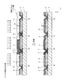
- FIG. 1 is a cross-sectional view schematically showing a main configuration of the display panel 100 according to the first embodiment.
- FIG. 2 is a perspective view showing a main configuration of the display panel 100.
- the display panel 100 is an organic EL display panel using an electroluminescence phenomenon of an organic material.
- pixels pixels
- each pixel is composed of adjacent RGB (red green blue) subpixels.
- the organic EL elements 20a, 20b, and 20c shown in FIG. 2 are top emission type organic EL elements.
- the organic EL element 20a is a first color (blue) sub-pixel
- the organic EL element 20b is a second color (green).
- the organic EL element 20c corresponds to a third color (red) subpixel.
- each organic EL element 20 is formed is referred to as an “element formation region”, and a region contributing to light emission in the element formation region is referred to as a “subpixel”.
- blue organic EL elements 20a are arranged in a line in the vertical direction (Y direction), and adjacent to them, green organic EL elements 20b ... are arranged in a line in the vertical direction (Y direction). Further, adjacent to the red organic EL elements 20b are arranged in a line in the vertical direction (Y direction).
- One pixel is formed by the three organic EL elements 20a, 20b, and 20c adjacent in the horizontal direction (X direction).
- FIG. 1 shows a cross section in which the arranged organic EL elements 20c... Are cut in the vertical direction (Y direction).
- the display panel 100 includes a TFT substrate including a substrate 1 and a TFT layer 2 (thin film transistor layer) stacked on the main surface of the substrate 1.
- the interlayer insulating film 3, the anode plate 5, the pixel regulating layer 6, and the hole injection layer 7 are sequentially laminated on the TFT substrate. Furthermore, partition walls 8, a hole transport layer 9, an organic light emitting layer 10 (hereinafter simply referred to as a light emitting layer), and a cathode layer 11 are formed thereon, thereby forming organic EL elements 20a, 20b, and 20c.
- FIG. 1 the side surface of the partition wall 8 on the far side of the cut surface is illustrated in white at the top in the Z-axis direction (the same applies to FIG. 3 and the like). Further, in FIG. 2, the hole transport layer 9, the light emitting layer 10, and the cathode layer 11 are not shown.
- the substrate 1 is a base portion of the display panel 100, and includes alkali-free glass, soda glass, non-fluorescent glass, phosphate glass, borate glass, quartz, acrylic resin, styrene resin, polycarbonate resin, It is formed of an insulating material such as epoxy resin, polyethylene, polyester, silicone resin, or alumina.
- the TFT layer 2 includes TFTs (thin film transistors) and wirings for driving the organic EL elements 20a to 20c of the entire panel by an active matrix method.
- TFTs thin film transistors
- FIG. 1 the TFT layer 2 is schematically shown by a two-dot chain line, and the SD electrode 22 connected to the source electrode or drain electrode of the TFT is representatively shown.
- the interlayer insulating film 3 is made of an organic material having excellent insulating properties, for example, polyimide, polyamide, and an acrylic resin material, and entirely covers the TFT layer 2 of the substrate 1.
- contact holes 13a, 13b, and 13c dug down in the thickness direction (Z direction) are formed for each of the organic EL elements 20a, 20b, and 20c (see FIGS. 1 and 3).
- the contact hole 13 is a circular hole opened on both the upper surface side and the lower surface side of the interlayer insulating film 3.
- the contact holes 13a, 13b, and 13c may be simply referred to as contact holes 13 without being distinguished from each other.
- the cross-sectional shape of the contact hole 13 (the cross-sectional shape parallel to the XY plane) may be oval or rectangular in addition to the circular shape.
- the contact hole 13 In the contact hole 13, the anode plate 5, the pixel restricting layer 6, and the hole injection layer 7 are recessed and stacked following the internal shape. As a result, the contact hole 13 and the hole injection layer 7 are A recess 15 having a similar shape is formed. In FIG. 2, since the contact hole 13 is hidden under the depression 15, the contact hole 13 is denoted by a broken lead line (the same applies to FIG. 3A).
- FIG. 3A is a plan view showing a schematic configuration of the display panel 100
- FIG. 3B is a cross-sectional view taken along the line AA ′ of FIG. 3A
- FIG. 3C is FIG. This is a cross section taken along line BB ′.
- the hole transport layer 9, the light emitting layer 10, and the cathode layer 11 are not shown.
- the interlayer insulating film 3 is mostly flat on the upper surface, but the portion where the contact hole 13 is formed is depressed.
- the contact holes 13 are arranged in a matrix like the organic EL elements 20.
- the contact holes 13 are arranged close to each other in the horizontal direction (X direction), and are arranged at an equal pitch with a predetermined separation distance in the vertical direction (Y direction).
- the upper areas of the contact holes 13a, 13b, and 13c corresponding to the respective colors are substantially the same (the upper areas will be described in detail later).
- the three contact holes 13a, 13b, and 13c have different shapes and volumes. Specifically, the contact hole 13a has no step and has a shape in which the cross section continuously narrows as it approaches the lower surface of the interlayer insulating film 3 (SD electrode side).
- the contact holes 13 b and c have a stepped surface 14, and have a shape in which the cross section becomes gradually narrower as it approaches the lower surface of the interlayer insulating film 3.
- the contact holes 13b and c are smaller in diameter in the lower part (the part below the step surface 14) than the contact hole 13a, and the volume is reduced as a whole. Further, the contact hole 13c has a smaller volume than the contact hole 13b.
- the volume (volume) of the contact holes 13a, 13b, and 13c corresponding to each color of blue, green, and red is set so that the volume of the contact hole 13a corresponding to blue is the largest, and the volume of the contact hole 13c corresponding to red is the largest. It is set small. For this reason, the volume of the depression 15a formed in the blue element formation region is the largest, and the volume of the depression 15c formed in the red element formation region is the smallest.
- the anode plate 5 (5a to 5c) is an example of an electrode plate and has a rectangular shape in plan view.
- the anode plate 5 is formed on the interlayer insulating film 3 in element formation regions (regions on the subpixel region and the contact hole 13) of each organic EL element 20.
- the anode plates 5 are equal in size and are arranged in a matrix in a state of being separated from other anode plates 5 by a predetermined distance in the vertical direction (Y direction) and the horizontal direction (X direction).
- a part of the anode plate 5 is recessed along the inner surface of the contact hole 13, thereby forming a recess 23 having a shape similar to that of the contact hole 13.
- the anode plate 5 is electrically connected to the SD electrode 22 of the TFT layer 2 at the bottom wall portion of the recess 23.
- the material forming the anode plate 5 is preferably light-reflective.
- silver-palladium-copper alloy, Ag (silver), silver-rubidium-gold alloy, MoCr (molybdenum and chromium alloy), Metal materials such as NiCr (alloy of nickel and chromium), aluminum, and aluminum alloy are used.
- a semiconductor material such as ITO (Indium Tin Oxide), IZO (In 2 O 3 —ZnO), ZnO, InO, or SnO may be used.
- the anode plate 5 may be formed by laminating the semiconductor material film on the metal material film.
- the pixel regulating layer 6 is an electrically insulating film extending in the horizontal direction (X direction), and covers the end of the anode plate 5 in the vertical direction (Y direction) and the recess 23.
- the electrical continuity between the anode plate 5 and the cathode layer 11 is cut off so that no light is emitted even when a driving voltage is applied to the organic EL element 20. . Therefore, a plurality of subpixels arranged in the vertical direction (Y direction) are partitioned by the pixel restriction layer 6.
- the pixel restricting layers 6 are equally spaced and arranged at equal pitches so that the sizes of the plurality of subpixels are uniform in the vertical direction (Y direction).
- the pixel restricting layer 6 covers the end portion and the depression 23 of the anode plate 5, thereby preventing the following luminance unevenness and short circuit between the anode plate 5 and the cathode layer 11. be able to. Specifically, when the film thickness of the light emitting layer 10 becomes thin above the edge of the anode plate 5 and the opening edge of the recess 23 and current is concentrated locally, the luminance increases locally and luminance unevenness occurs. To do. In addition, if the light emitting layer 10 or other layers are interrupted above the edge of the anode plate 5 or the opening edge of the recess 23, a short circuit may occur between the anode plate 5 and the cathode layer 11.
- the pixel restriction layer 6 is an insulating inorganic film formed of silicon oxide (SiO 2 ), silicon nitride (SiN), silicon oxynitride (SiON), or the like. Its thickness is about 100 nm to 300 nm.
- the hole injection layer 7 (7a to 7c) is formed by laminating an oxide such as molybdenum or tungsten on the anode plate 5 and the pixel regulating layer 6.
- the hole injection layer 7 is recessed into the recess 23 of the anode plate 5 together with the pixel regulation layer 6 in the region on the contact hole 13 to form a recess 15 having a shape similar to the recess 23.
- the film thickness of the pixel restricting layer 6 and the hole injection layer 7 is much smaller than the size (diameter and depth dimension) of the depression 23, so that the depression 15 formed in the hole injection layer 7 has a smaller thickness.
- the volume and the volume of the recess 23 formed in the anode plate 5 are substantially the same.
- the partition walls 8 (8a to 8c) are made of an insulating organic material (for example, acrylic resin, polyimide resin, novolac type phenol resin, etc.), and are formed so that at least the surface has liquid repellency.
- Each of the partition walls 8a, 8b, and 8c has a long line shape in the vertical direction (Y direction), and passes between the organic EL elements 20a, 20b, and 20c continuously arranged in the horizontal direction (X direction). Thus, they are formed at equal pitches in the lateral direction (X direction).
- Each partition wall 8a, 8b, 8c has a trapezoidal cross-sectional shape, and each partition wall width (dimension in the X direction) is uniform.
- the hole transport layer 9 (9a to 9c) is an example of the organic functional layer, and is formed so as to cover the hole injection layer 7 in a region sandwiched between adjacent partition walls 8. Each hole transport layer 9 partially enters the depression 15 on the pixel regulation layer 6.
- the hole transport layer 9 is formed continuously in the vertical direction (Y direction).
- the thickness of the hole transport layer 9 in the light emitting region or the like differs because the volume of the recess 15 varies depending on the volume of the contact holes 13a, 13b, 13c corresponding to each color.
- a hole transport layer 9a corresponding to blue is formed between the partition walls 8a and 8b, and a hole transport layer 9b corresponding to green is formed between the partition walls 8b and 8c.
- a hole transport layer 9c corresponding to red is formed between 8c and the partition wall 8a.
- the light emitting layer 10 (10a to 10c) is formed on the hole transport layer 9 in a region sandwiched between adjacent partition walls 8. Each light emitting layer 10 partially enters the recess 15 together with each hole transport layer 9.
- a light emitting layer 10a that emits blue light is formed above the hole transport layer 9a
- a light emitting layer 10b that emits green light is formed above the hole transport layer 9b
- a light emitting layer 10c that emits red light is formed.
- the hole transport layer 9 is made of a material having excellent hole mobility, and transports holes to the light emitting layer 10.
- the material for forming the hole transport layer 9 include 4,4′-bis [N- (naphthyl) -N-phenyl-amino] biphenyl ( ⁇ -NPB or ⁇ -NPD), N, N′-bis.
- triarylamine compounds such as (3-methylphenyl)-(1,1′-biphenyl) -4,4′-diamine (TPD).
- Other examples include biphenyl derivatives, anthracene derivatives, aniline derivatives, thiophene derivatives, and the like.
- the anode plate 5, the hole injection layer 7, and the hole transport layer 9 are made of the same material for the three-color organic EL elements 20a, 20b, and 20c, but the light-emitting layer 10 has the three-color organic EL element.
- 20a, 20b, and 20c are formed of light emitting materials that emit blue, green, and red light separately.
- Examples of the material of the light emitting layer 10 include an oxinoid compound, a perylene compound, a coumarin compound, an azacoumarin compound, an oxazole compound, an oxadiazole compound, a perinone compound, a pyrrolopyrrole compound, a naphthalene compound described in JP-A-5-163488.
- the cathode layer 11 is an example of a counter electrode, and is formed so as to collectively cover the light emitting layers 10 of the three-color organic EL elements 20a, 20b, and 20c.
- the cathode layer 11 is formed of a light transmissive material such as ITO or IZO (indium zinc oxide).
- a sealing layer is provided on the cathode layer 11.
- the sealing layer is formed of a light transmissive material such as SiN (silicon nitride) or SiON (silicon oxynitride).
- the pitches and the widths of the partition walls 8 are equal, and the pitch and width of the pixel regulation layer 6 are also uniform. Therefore, the subpixels surrounded by the partition walls 8 and the pixel regulation layer 6 The size is even.
- a plurality of blue anode plates 5a are arranged in a vertical (Y direction) line shape to form a first anode plate group (first electrode plate group). Is an example). Adjacent to the first anode plate group, a plurality of green anode plates 5b are arranged in a vertical (Y direction) line shape to form a second anode plate group (which is an example of a second electrode plate group). Has been. A plurality of red anode plates 5c are arranged in a vertical (Y direction) line shape adjacent to the second anode plate group to form a third anode plate group (which is an example of a third electrode plate group). ing.
- each anode plate group is a rectangle elongated in the vertical direction (Y direction), and each anode plate group has two long side portions in total on the left and right.
- a first partition (partition 8a) is formed along one (left side) long side portion of the first anode plate group, and the other (right side) long side portion and second anode plate group of the first anode plate group.
- a second partition wall (partition wall 8b) is formed between one (left side) and the long side part of the second anode plate group, and the other side (right side) of the second anode plate group and one side (left side) of the third anode plate group.
- a third partition (partition 8c) is formed between the first and second long sides, and a fourth partition (partition 8a) is formed along the other (right) long side of the third electrode plate group. Note that the fourth partition (partition 8a) becomes the first partition (partition 8a) in the adjacent pixel.
- TFT layer forming process A TFT layer 2 composed of TFTs, wirings, and SD electrodes 22 is formed on the substrate 1 by a known manufacturing method (for example, described in Japanese Patent Application Laid-Open Nos. 2003-241683 and 2008-300611). 4 (a)).
- TFT, SD electrode 22, wiring, etc. are formed by sputtering method, CVD method (chemical vapor deposition method) or the like.
- a gate electrode, a gate insulating film, a source, a drain, a channel layer, and the like are formed.
- the SD electrode 22 is formed so as to be electrically connected to either the source or the drain.
- the wiring for example, a plurality of signal wirings extending in the Y direction and a plurality of scanning wirings extending in the X direction are formed and connected to each TFT.
- the TFT may be a top gate type in which a gate electrode is formed above a source, a drain, or the like, or may be a bottom gate type in which a gate electrode is formed below a source, a drain, or the like.
- Interlayer insulation film formation process After applying a resist film 26 made of a positive photosensitive organic material on the TFT layer 2, a contact hole 13 is formed in a portion of the resist film 26 located on the SD electrode 22.
- the resist film 26 is applied by a liquid layer film forming method such as a spin coating method, and the surface of the TFT layer 2 is flattened by filling the unevenness on the TFT layer 2.
- a liquid layer film forming method such as a spin coating method
- coat by liquid layer film-forming methods such as the dip coat method, the slit coat method, the spray coat method, the roll coat method, and the die coat method.
- a photolithography method is used to form the contact hole 13.
- an upper portion and a lower portion are formed above and below the step surfaces 14b and 14c, respectively (see FIG. 5).
- the upper part and the lower part are separately formed in two steps. For example, after forming an upper portion having a large opening diameter by the first exposure and development processing, a lower portion having a small opening diameter is formed again by the exposure and development processing.
- FIGS. 5A and 5B are cross-sectional views schematically showing a process for forming the contact hole 13 using a photolithography method.
- the multi-tone mask 30 used for the exposure process includes a light-transmitting part 31 that transmits light, a semi-light-transmitting part 32 that weakens transmitted light, and a light-shielding part 33 that blocks light.
- the semi-translucent portion 32 has a pattern that is sufficiently finer than the resolution of the exposure machine, the transmittance is adjusted by adjusting the number of fine patterns arranged per unit area, and has a predetermined transmittance.
- the multi-tone mask 30 in the case where the volume of the contact hole 13 is different for each RGB is arranged with a pattern sufficiently finer than the resolution of the exposure machine, and the number of fine patterns arranged per unit area is adjusted for transmission. What adjusted the rate is suitable.
- each contact hole 13 the opening diameter of each of the translucent portions 31a, 31b, 31c is set so that the lower openings 35a, 35b, 35c of the contact holes 13a, 13b, 13c (openings on the substrate 1 side or bottom surface). ) Is substantially the same as the diameter.
- the outer diameters of the semi-translucent portions 32b and 32c are substantially the same as the outer diameters of the step surfaces 14b and 14c (corresponding to the bottom surface of the upper portion) of the contact holes 13b and 13c.
- a portion other than the light transmitting portion 31 and the semi-light transmitting portion 32 is a light shielding portion 33.
- the light transmitting portion 31 has a high light transmittance, and the portion of the resist film 26 irradiated with the light transmitted through the light transmitting portion 31 opens on the lower surface side of the resist film 26 after the development process.
- the irradiation light is weakened in the semi-translucent portion 32, the upper portion of the portion irradiated with the light transmitted through the semi-transparent portion 32 is removed after the development processing to form stepped surfaces 14b and 14c.
- the multi-tone mask 30 By exposure with the multi-tone mask 30, the range schematically shown by the two-dot chain lines 36a, 36b, 36c in FIG. 5A is exposed and dissolved in the development process.
- the contact hole 13 can also be formed by a method in which a portion where the contact hole 13 is to be formed is removed by etching after an insulating film having a flat upper surface is formed.
- a photoresist is applied on the insulating film in an overlapping manner, and a pattern mask corresponding to the contact hole 13 to be formed is overlaid thereon.
- a pattern mask for the upper portion and a pattern mask for the lower portion are necessary.
- the contact hole 13a having no step can be shared with the pattern mask for the lower portion of the contact holes 13b and 13c.
- a resist pattern is formed by removing the photosensitive portion (or non-photosensitive portion) of the photoresist by development processing. Thereafter, a portion exposed in the opening portion of the resist pattern in the insulating film is removed by, for example, wet etching (or dry etching), thereby forming an upper portion (lower portion, contact hole 13a) in the insulating film.
- the interlayer insulating film 3 can be formed by patterning the insulating film by performing such exposure and development processes twice.
- Anode plate forming process A metal material (silver, palladium and copper alloy) is formed into a thickness of about 100 to 200 nm on the interlayer insulating film 3 by sputtering, and a semiconductor material (IZO) is thinned to a thickness of about 90 nm on the metal material film. Mold.
- a metal material silver, palladium and copper alloy
- IZO semiconductor material
- anode plates 5 having a rectangular shape in plan view arranged in a matrix are formed by photolithography. Specifically, a resist film is formed on a semiconductor material film, the resist film is exposed using a mask pattern in which rectangular anode plate shapes are arranged in a matrix, and then exposed to TMAH (tetramethylammonium hydroxide). The part is dissolved and removed and developed. Further, by removing and patterning the lattice-shaped portion of the metal material film and the semiconductor material film that are not covered with the resist film by wet etching (for example, an aqueous solution of phosphoric acid, nitric acid, and acetic acid), the rectangular anode A plate 5 is formed.
- TMAH tetramethylammonium hydroxide
- the anode plate 5 is also formed on the inner surface of the contact hole 13, the anode plate 5 is recessed along the inner surface of the contact hole 13, and a recess 23 is formed in the anode plate 5.
- the bottom wall portion of the recess 23 is electrically connected in surface contact with the SD electrode 22 through the lower opening of the contact hole 13 (FIG. 4C).
- Pixel regulation layer formation process Next, SiON is formed to a thickness of 100 to 300 nm by CVD. Thereafter, the pixel regulation layer 6 is formed by patterning by dry etching using a photolithography method (FIG. 4E).
- Hole injection layer forming step Next, a hole injection layer 7 is formed on the anode plate 5 and the pixel regulating layer 6 by forming a metal oxide film such as molybdenum oxide or tungsten oxide by a reactive sputtering method. (FIG. 4 (d)).
- a metal oxide film such as molybdenum oxide or tungsten oxide by a reactive sputtering method.
- the pixel regulation layer 6 and the hole injection layer 7 are also partially recessed along the anode plate 5 into the recessed portions 23a, 23b, and 23c. As a result, depressions 15 a to 15 c are formed in the hole injection layer 7.
- the pixel regulation layer 6 and the hole injection layer 7 have the same film thickness in the sub-pixel and the film thickness in the depression 23.
- Partition formation process Next, as the partition wall material, for example, a photosensitive resist material or a resist material containing a fluorine-based or acrylic-based material is applied on the interlayer insulating film 3 and patterned by a photolithography method, thereby partition walls 8a, 8b, 8c is formed (FIG. 4F).
- the partition wall material for example, a photosensitive resist material or a resist material containing a fluorine-based or acrylic-based material is applied on the interlayer insulating film 3 and patterned by a photolithography method, thereby partition walls 8a, 8b, 8c is formed (FIG. 4F).
- the surface of the partition wall 8 is surface-treated with an alkaline solution, water, an organic solvent or the like, or subjected to plasma treatment in order to impart liquid repellency to the ink applied in the next step. Also good.
- hole transport layer 9 is formed by an inkjet method (inkjet application method) (FIG. 4G).
- an organic material that is a hole transport layer material and a solvent are mixed at a predetermined ratio to prepare an ink for a hole transport layer, and the ink is applied between adjacent partition walls 8. That is, according to a known inkjet method, the partition wall 8a as the first partition wall and the partition wall 8b as the second partition wall, the partition wall 8b as the second partition wall and the partition wall 8c as the third partition wall, and the third partition wall. Ink is applied along a region between a certain partition wall 8c and the fourth partition wall 8a.
- FIG. 6 is a schematic cross-sectional view showing a state immediately after the ink for forming the hole transport layer is applied on the substrate by the inkjet method. In FIG. 6, the hole injection layer 7 is not shown.
- each arrow indicates that ink is dropped from a nozzle of the ink jet apparatus to a plurality of predetermined locations in each element formation region. That is, the number of droplets dropped onto each element formation region (for example, 8 droplets) and a plurality of locations where droplets are dropped on each element formation region are made equal. As a result, the applied ink covers the entire top of the hole injection layer 7 and also enters the recess 15 formed by the presence of the contact hole 13.
- the amount of each ink droplet ejected from the nozzle is constant, the amount of ink applied is uniform in a plurality of element formation regions. That is, the amount of ink applied above each anode plate 5 is the same, and the variation is within 5%.
- a dispenser method for forming the hole transport layer 9 between the banks
- a nozzle coating method for forming the hole transport layer 9 between the banks
- the amount of ink applied on the injection layer 7 is the same for all color sub-pixels.
- the hole transport layer 9 is formed by drying the ink layer thus formed.
- Light emitting layer forming process A light emitting layer 10 is formed on the hole transport layer 9 by an inkjet method. This step is the same as the hole transport layer forming step, and is formed by applying an ink in which an organic light emitting material for forming a light emitting layer is dissolved between adjacent partition walls 8 and drying. The organic light emitting material to be used is different for each emission color.
- the light emitting layer 10 made of a low molecular weight organic light emitting material can be formed on the hole transport layer 9 by, for example, a vacuum deposition method.
- a dispenser method, a nozzle coating method, a printing method, or the like may be used as a method of filling the ink for forming the light emitting layer 10 between the banks.
- Cathode layer forming process, etc . Next, a material such as ITO or IZO is formed on the surface of the light emitting layer 10 by sputtering or vacuum deposition. Thereby, the cathode layer 11 is formed. Further, a sealing layer is formed on the surface of the cathode layer 11 by depositing a material such as SiN (silicon nitride) or SiON (silicon oxynitride) by sputtering or vacuum deposition.
- a material such as ITO or IZO is formed on the surface of the light emitting layer 10 by sputtering or vacuum deposition.
- the cathode layer 11 is formed.
- a sealing layer is formed on the surface of the cathode layer 11 by depositing a material such as SiN (silicon nitride) or SiON (silicon oxynitride) by sputtering or vacuum deposition.
- the volume of the contact hole 13 is set to be the largest for the contact hole 13a corresponding to blue and the smallest for the contact hole 13c corresponding to red (13a>13b> 13c). Therefore, the volume of the hollow portion 15 is the largest at the hollow portion 15a formed above the contact hole 13a and the smallest at the hollow portion 15c formed above the contact hole 13c (15a>15b> 15c).
- the hole transport layers 9a, 9b and 9c corresponding to the respective colors have the same volume in the region above each anode plate 5, but the volumes (amounts) entering the recesses 15a, 15b and 15c are different.
- the film thickness of the hole transport layer 9a of the blue subpixel (the film thickness in the region other than the depression 15 in the region on the anode plate 5) is the smallest, and the film thickness of the hole transport layer 9b of the green subpixel is It becomes an intermediate thickness, and the film thickness of the hole transport layer 9c of the red subpixel is the thickest.
- the difference in film thickness between the hole transport layers 9a, 9b, and 9c can be finely adjusted by changing the volumes of the recesses 15a, 15b, and 15c. Therefore, in the display panel 100, it is easy to set the film thickness of the hole transport layer 9 to an appropriate value that matches the wavelength of the luminescent color for each subpixel color.
- the recess 15 is formed by recessing the hole injection layer 7 recessed in the recess 23 formed in the anode plate 5 along the shape of the recess 23. Since the pixel restricting layer 6 and the hole injection layer 7 are formed by CVD or sputtering, the shape of the recess 15 is very similar to that of the recess 23. Further, the film thickness of the hole injection layer 7 or the like is much smaller than the size (diameter and depth) of the recess 23, and the influence on the volume of the recess 23 is small.
- the first, second, and third depressions are respectively constituted by depressions 23a, 23b, and 23c, but for convenience, the first, second, and third depressions are respectively You may think that the hollow parts 15a, 15b, and 15c comprise.
- the calculation is performed without considering the gap.
- the film thickness of the hole transport layer 9 in the subpixel is simply referred to as the film thickness of the hole transport layer 9.
- the area of the ink application region on the anode plate 5 (the region indicated by reference numeral 5 in FIG. 3A) is S, and the solute concentration of the intermediate layer ink is N. Further, the amount of ink applied to one ink application area (shaded area C in FIG. 6) is V0, and the volume of the depression 15 formed on the anode plate 5 is V1 (the depression 15a corresponding to each color). , 15b and 15c are defined as V1a, V1b and V1c, respectively.
- FIG. 7A shows a state before and after drying of the ink when it is assumed that the recess 15 is not formed. If the entire upper surface of the anode plate 5 is flat and there is no depression, the virtual height H0 of the ink layer applied above the anode plate 5 can be obtained by dividing the coating amount V0 by the area S.
- H0 V0 / S (1-1)
- the virtual film thickness h0 of the hole transport layer 9 formed after drying is obtained by multiplying the virtual height H0 of the ink layer by the solute concentration N.
- FIGS. 7B and 7C show states before and after drying of the ink when the recess 15 is formed.
- a portion where the ink filled in the depression 15 is dried and a portion where the ink layer above the depression 15 is dried are shown separately. This will be described later.
- the ink layer height H in the sub-pixel is applied on the anode plate having no recess by applying the ink remaining amount (V0 ⁇ V1) obtained by subtracting the ink application amount V0 from the filling amount V1 to the recess 15. It can be regarded as the same as the height in the case (see FIG. 7B).
- the height H of the ink layer is obtained by dividing the remaining ink amount (V0 ⁇ V1) by the area S by the following equation.
- the virtual film thickness h0 of the hole transport layer 9 is N ⁇ V0 / S as described above. Therefore, in comparison with the virtual film thickness h0, the amount E in which the film thickness h of the hole transport layer 9 is reduced due to the presence of the recess 15 is expressed by the following equation.
- the reduction amount E of the film thickness h with respect to the virtual film thickness h0 of the hole transport layer 9 is determined based on the volume of the recess 15 in principle. Therefore, if the volume (V1) of the hollow portion 15 is increased, the reduction amount E of the film thickness h of the hole transport layer 9 with respect to the virtual film thickness h0 can be increased.
- the magnitudes of the volumes V1a, V1b, V1c of the dents 15 of each color are V1a> V1b> V1c. Therefore, for example, when the ink application amount V0 and the solute concentration N are the same, the film thickness of the hole transport layer 9a of the blue subpixel is the smallest, and the film thickness of the hole transport layer 9c of the red subpixel is the smallest. Become thicker.
- FIGS. 7B and 7C show the heights Ha and Hb of the ink layer and the hole transport.
- the film thicknesses ha and hb of the layers 9a and 9b are shown.
- the anode plate 5 and the like are not shown, and the cross-sectional shape of the recess 15 is rectangular.
- the ink application amount V0 and the solute concentration N are equal to each other in each color ink application region.
- the film thickness difference ⁇ hab between the film thickness ha of the hole transport layer 9a in the blue subpixel and the film thickness hb of the hole transport layer 9b in the green subpixel is obtained by the following equation.
- the film thickness difference ⁇ h (for example, ha ⁇ hb) between hb and hc can be adjusted.
- the volume V1a of the hollow portion 15a is larger than the volume V1b of the hollow portion 15b, a negative value is obtained when the volume V1a is subtracted from the volume V1b. This is because the film thickness ha is smaller than the film thickness hb. It is shown that.
- the film thickness difference ⁇ h can be adjusted by the same principle.
- each recess 15 is defined by the size of the contact hole 13 formed in the interlayer insulating film 3, and can be finely adjusted as will be described later. It is. Accordingly, the volume V1a, V1b, V1c of the depression can be adjusted in fine units as compared with the volume of one ink droplet, so that the film thickness difference of the hole transport layer 9 having different corresponding colors can be finely adjusted. .
- the film thickness is adjusted by changing the number of ink droplets to be applied for each subpixel color.
- the number of ink droplets applied to each ink application region is M
- the volume of one ink droplet is a value obtained by dividing the ink application amount V0 by the number M of ink droplets (V0 / M). Therefore, when the number of ink droplets applied to each ink application region is increased or decreased by 1 (for example, when comparing M and M + 1 droplets), the film thickness of the formed intermediate layer is N (V0 / Since it is increased or decreased by M) / S, the film thickness difference can be adjusted only in units of N (V0 / M) / S.
- the volume difference (for example, V1a ⁇ V1b) between the depressions 15a, 15b, and 15c is adjusted by a unit smaller than the volume (V0 / M) of one drop of ink.
- V0 / M volume of ink half-drop V0 / 2M. Therefore, the film thickness difference ⁇ h of the hole transport layer 9 can be set to be smaller than the film thickness difference when the number of ink droplets is increased or decreased by, for example, N (V 0 / 2M) / S.
- the film thickness difference ⁇ h of the hole transport layer 9 is larger than, for example, the film thickness difference when the number of ink droplets is increased or decreased by n drops, and the film thickness difference when the number of droplets is increased or decreased by n + 1 drops. It can also be set small.
- the film thickness difference ⁇ hab between the film thickness ha of the hole transport layer 9a of the blue subpixel and the film thickness hb of the hole transport layer 9b of the green subpixel is dropped on the (ii) blue subpixel.
- the thickness of the hole transport layer 9a is larger than the increase in the film thickness ha of the hole transport layer 9a when the number of ink droplets is increased by n and the number of ink droplets is increased by n + 1 droplets. It can be made smaller than the increase in ha.
- the thickness of the hole transport layer 9 in the recess 15 is approximately equal to the subpixel. It becomes thicker than the film thickness of the hole transport layer 9. This is due to the ink filled in the recess 15.
- the amount (volume) v3 of the hole transport layer 9 entering the recess 15 indicates the volume of the portion sandwiched between the straight line E and the straight line F. That is, the amount of the hole transport layer 9 entering the recess 15 can be expressed as the amount of the hole transport layer 9 formed in the same region as the recess 15 in plan view.
- the amount (volume) v3 of the hole transport layer 9 entering the recess 15 is the first portion 42 formed by drying the first ink portion 41 (volume V1) filled in the recess 15. And the volume v2 of the second portion 44 obtained by drying the second ink portion 43 (volume V2) located above the recess 15 in the ink layer.
- v3 v1 + v2 (3-1) Note that the volume v1 and the volume v2 are expressed by the following equations.
- the volume v1 of the first portion 42 contributes to the change in the film thickness h of the hole transport layer 9. And as a result of adjusting the volume V1 of the hollow part 15, the volume v1 of the 1st part 42 is optimized, and the film thickness h of the hole transport layer 9 can be made appropriate.
- the difference between the volumes V1a and V1b of the first ink portions 41a and 41b corresponding to each color the difference between the volumes v1a and v1b of the first portion 42 is optimized, and hole transport in the sub-pixels of each color.
- the film thickness difference between the layers 9a, 9b and 9c is finely adjusted.
- the volume equivalent value v2 'corresponding to the volume v2 of the second portion 44 is calculated based on the amount of the hole transport layer 9 in the subpixel.
- the height of the second ink portion 43 is the same as the height H of the ink layer 45 in the sub-pixel. Therefore, assuming that the upper area of the depression 15 is S1, the volume v4 per area S1 of the hole transport layer 9 (portion illustrated by reference numeral 46) corresponds to the volume v2 of the second portion 44 in the subpixel.
- the volume equivalent value v2 ′ is considered.
- the volume v4 can be calculated by multiplying the film thickness h of the hole transport layer 9 in the subpixel by the area S1.
- the film thickness h can be made into the average film thickness of the film thickness of the hole transport layer 9 in a sub pixel, for example.
- the film thickness of the hole transport layer 9 in the subpixel can be measured at a plurality of locations, and the average value can be obtained.
- the volume equivalent value v2 ′ of the second ink portion 43 is obtained, and the volume equivalent value v1 ′ of the first ink 41 can be calculated.
- the equivalent value v3 ′ of the total volume v3 can be calculated based on, for example, the cross section of the hole transport layer 9 that has entered the recess 15. Specifically, for example, when a cross section including the central axis of the hollow portion 15 is obtained, the volume of the rotating body obtained by rotating the cross sectional shape of the hole transport layer 9 once around the central axis is set to the equivalent value v3 ′. Can do.
- the volume equivalent value v1 ′ and the volume v1 obtained by multiplying the hollow portion 15a volume V1 by the solute concentration N are approximately the same value (for example, within a range of ⁇ 10%).
- the upper area S1 of the depression 15 can be defined in the same way as the upper area of the contact hole 13 described later. That is, it is good also as an area of the circle prescribed
- the volume (V1a) of the first contact hole (13a) is larger than the volume (V1b) of the second contact hole (13b), and [ii] the electrode for the first color
- the volume (for example, N ⁇ V0) of the first organic functional layer (9a) corresponding to the region on the plate (5a) is the second region corresponding to the region on the second color electrode plate (5b). It is within the range of the same or the same value as the volume (for example, N ⁇ V0) of the organic functional layer (9b), and [iii] the film thickness (ha) of the first organic functional layer is the first contact hole.
- the volume (V1a) of the first contact hole (13a) is larger than the volume (V1b) of the second contact hole (13b), and [ii] the first color for the first color
- the difference (v3b ⁇ v2b v1b) from the amount (v
- the volumes v1, v2, and v3 in the parentheses can be set to the aforementioned volume equivalent values v1 ', v2', and v3 '.
- the hole transport layer 9a in the blue sub-pixel corresponds to the first organic functional layer
- the hole transport layer 9b in the green sub-pixel corresponds to the second organic functional layer
- the red The hole transport layer 9c in the subpixel corresponds to the third organic functional layer.
- the hole transport layer 9a in the blue sub-pixel corresponds to the first organic functional layer
- the hole transport layer 9c in the red sub-pixel corresponds to the second organic functional layer
- the hole transport layer 9b in the green sub-pixel corresponds to the first organic functional layer
- the hole transport layer 9c in the red sub-pixel corresponds to the second organic functional layer.
- the solute concentration N of the ink for the intermediate layer is 0.02 (2 vol%)
- the amount of droplets ejected by inkjet is 3 pL
- the film thickness h0 is obtained by the following equation.
- the depression 15a corresponding to blue has a truncated cone shape whose upper surface radius is larger than the lower surface radius, the upper surface radius r1 is 20 ⁇ m, the lower surface radius r2 is about 17.7 ⁇ m, the height T is 4 ⁇ m, and the inclination angle of the side surface was 60 [°] (inclination angle with respect to the XY plane).
- the volume V1a of the hollow portion 15a is obtained by the following equation. When ⁇ is 3.14, the volume V1a is 4468 ⁇ m 3 (4.468 pL).
- V1 ⁇ ⁇ T (r 1 2 + r 1 ⁇ r 2 + r 2 2 ) / 3 (3-2)
- the film thickness ha of the hole transport layer 9a of the blue subpixel is obtained by the following equation.
- the hollow portion 15b corresponding to green has a shape in which two truncated cones whose upper diameters are enlarged are stacked one above the other, and the upper and lower portions are calculated separately.
- the upper truncated cone part had an upper surface radius of 20 ⁇ m, a lower surface radius of about 19.1 ⁇ m, a height of 1.5 ⁇ m, and a side surface inclination angle of 60 ° (inclination angle with respect to the XY plane).
- the lower truncated cone part had an upper surface radius of 15 ⁇ m, a lower surface radius of about 13.6 ⁇ m, a height of 2.5 ⁇ m, and a side surface inclination angle of 60 ° (an inclination angle with respect to the XY plane).
- the volume of the upper truncated cone part is 1800 ⁇ m 3 (1.800 pL), and the volume of the lower truncated cone part is 1607 ⁇ m 3 (1.607 pL). Therefore, the volume V1b of the depression 15b is 3407 ⁇ m 3 (3.407 pL).
- the film thickness hb of the hole transport layer 9b of the green subpixel is obtained by the following equation.
- the recess 15c corresponding to red also has a shape in which two truncated cones whose upper diameters are enlarged are stacked one above the other, and the upper and lower portions are calculated separately.
- the upper truncated cone part had an upper surface radius of 20 ⁇ m, a lower surface radius of about 19.1 ⁇ m, a height of 1.5 ⁇ m, and a side surface inclination angle of 60 ° (inclination angle with respect to the XY plane).
- the lower truncated cone part had an upper surface radius of 10 ⁇ m, a lower surface radius of about 8.6 ⁇ m, a height of 2.5 ⁇ m, and a side surface inclination angle of 60 ° (inclination angle with respect to the XY plane).
- the volume of the upper truncated cone part is 1800 ⁇ m 3 (1.800 pL), and the volume of the lower truncated cone part is 680 ⁇ m 3 (0.680 pL). Accordingly, the volume V1c of the recess 15c is 2480 ⁇ m 3 (2.480 pL).
- the film thickness hc of the hole transport layer 9c of the red subpixel is obtained by the following equation.
- the film thickness difference ⁇ hab between the film thickness ha of the hole transport layer 9a of the blue subpixel and the film thickness hb of the hole transport layer 9b of the green subpixel is 1.0 nm.
- the film thickness difference ⁇ hbc between the film thickness hb and the film thickness hc is 0.9 nm.
- the film thickness difference ⁇ hac between the film thickness ha and the film thickness hc is 1.9 nm.
- the volume difference ⁇ V1 of the contact hole 13 is about 1000 ⁇ m 3 (1 pL) for ⁇ V1ab (blue and green) and ⁇ V1bc (green and red) and about 2000 ⁇ m 3 (2 pL) for ⁇ V1ac (blue and red), respectively. .
- the film thickness difference of the hole transport layer 9 between the sub-pixels of each color can be adjusted by a minute unit (for example, 1 nm or less).
- the thickness of the formed intermediate layer is increased or decreased by about 2.9 nm.
- the film thickness can be adjusted only in units.
- the volume of the recesses 15a, 15b, and 15c formed in each color subpixel is finely adjusted more finely than the volume of the ink droplet, thereby making each color subpixel.
- the film thickness difference of the hole transport layer 9 of the pixel can be finely adjusted relatively easily. As a result, it becomes easy to efficiently extract light by setting the film thickness of the hole transport layer 9 to an appropriate value corresponding to the wavelength of the emission color for each color of the subpixel.
- the inclination (taper angle) of the side surface of the contact hole 13 is 60 degrees, but is not limited to 60 degrees and can be an arbitrary inclination angle. Furthermore, the inclination angle may be different between the upper part and the lower part.
- the film thickness difference ⁇ h is not limited to 1 nm or 2 nm, and can be, for example, less than 1 nm or 3 nm or more depending on conditions.
- the upper surface radius of the contact hole 13 is not limited to 20 ⁇ m, and may be an arbitrary value such as 25 ⁇ m or more.
- the upper opening of the contact hole 13 is preferably formed apart from the region where the partition wall 8 is formed in plan view so as not to affect the height and shape of the partition wall 8.
- the volume difference ⁇ V1 between the contact holes 13 having different colors is preferably larger than the volume error of the contact hole 13a.
- the volume difference ⁇ V1ab exceeds the 450 [mu] m 3.
- the upper areas of the contact holes 13a, 13b, 13c corresponding to the respective colors are substantially the same.
- the upper area of the contact hole 13 is a circle area defined by the diameter of the contact hole 13 at a position about 10% lower than the highest position of the peripheral edge of the contact hole 13.
- FIGS. 8A, 8B, and 8C are diagrams schematically showing a cross section of the contact hole 13, respectively (note that the cross section of the contact hole 13b is representatively shown).
- the shape of the contact hole 13 in each figure differs in a peripheral part. In such a case, how to define the diameter of the contact hole 13 will be described.
- the highest position of the peripheral edge of the contact hole 13 is the same height (straight line O1) as the upper surface 50 of the interlayer insulating film 3.
- FIG. The position lowered by 10% is 10% (P1 / 10) of the depth P1 of the contact hole 13, and is indicated by a straight line Q1. Therefore, in the cross section of the drawing, the distance between the two intersections of the straight line Q1 and the side surface of the contact hole 13 is the diameter ⁇ 1 of the contact hole 13.
- the upper area of the contact hole 13 is, for example, the area of a circle having a diameter ⁇ 1.
- the opening edge of the contact hole 13 is a curved portion 51.
- the curved portion 51 constitutes the peripheral portion of the contact hole 13 and is the highest position of the curved portion 51, that is, the height position of the upper surface 50 of the interlayer insulating film 3.
- the position lowered by 10% is the position (Q2) lowered by 10% (P2 / 10) of the depth P2 from the upper surface 50 of the interlayer insulating film 3 in the same manner as Q1. Therefore, in the cross section of the drawing, the distance between the two intersections between the straight line Q2 and the side surface of the contact hole 13 is the diameter ⁇ 2 of the contact hole 13.
- a raised portion 52 is formed adjacent to the contact hole 13.
- the position of the top portion 54 of the raised portion 52 corresponds to the highest position of the peripheral edge portion of the contact hole 13.
- the depth P3 of the contact hole 13 is a distance P3 from the top 54 to the bottom of the raised portion 52. Therefore, a position that is lowered by about 10% from the highest position is a position (Q3) that is 10% (P3 / 10) lower than the top 54 of the depth P3.
- the distance between the two intersections of the straight line Q2 and the side surface of the contact hole 13 is the diameter ⁇ 3 of the contact hole 13.
- FIG. 9 is a cross-sectional view schematically showing an optical path of light in the organic EL element 20.
- This figure shows direct light 61 directly emitted from the light emitting layer 10 to the cathode layer 11 side and reflected light 62 emitted after being reflected on the anode plate 5 side.
- the anode plate 5 is shown divided into a metal layer 63 and a transparent electrode layer 64 (IZO).
- IZO transparent electrode layer 64
- the reflection surface of the anode plate 5 is constituted by the main surface of the metal layer 63 on the transparent electrode layer 64 side.
- the light resonance conditions in the organic EL element 20 can be optimized with respect to the optical path lengths of the hole transport layer 9, the hole injection layer 7, and the transparent electrode layer 64.
- Such a structure is called a cavity or cavity structure.
- the optical path difference may be adjusted only by the film thickness of the hole transport layer 9, or in addition to the hole transport layer 9, the film thickness of the hole injection layer 7, the transparent electrode layer 64, etc. is also adjusted to adjust the optical path. The difference may be adjusted.
- ⁇ Briefly describe how to determine the difference in contact hole volume. For example, manufacture a prototype of an organic EL display panel and how to change the thickness difference of the organic functional layer of each color in order to optimize the light resonance condition for each color, or the thickness of the organic functional layer Whether to change the film thickness as a whole while maintaining the difference is determined. Then, an organic EL display panel is manufactured by changing the volume of the contact hole under the same manufacturing conditions (ink application conditions) as the prototype. In this manner, the light resonance condition in the organic EL element is optimized, and an organic EL display panel with high luminous efficiency is obtained.
- the contact holes 13b and 13c have an upper stage portion and a lower stage portion, and the upper surface radius of the lower stage portion is different.
- the volume of the contact hole 13 can be made different also by changing the depth of the upper part and the lower part.
- FIG. 10 is a cross-sectional view schematically showing portions corresponding to the contact holes 13b and 13c in FIG.
- a contact hole 13d is formed instead of the contact hole 13b of the above embodiment.
- the contact hole 13c is the same as that shown in FIG.
- the contact hole 13d has a depth in the upper part above the step surface 14d that is deeper than the upper part of the contact hole 13c. By doing so, the volume of the contact hole 13d can be made smaller than the contact hole 13a and larger than the contact hole 13c.
- the multi-tone mask 70 includes light-transmitting portions 71 and 72 that transmit light, a first semi-transmitting portion 73 having a low light transmittance, and a light transmittance that is lower than that of the first semi-transmitting portion 73. It consists of two semi-translucent portions 74 and a light shielding portion 75 that blocks light.
- the translucent part 71 and the first semi-transparent part 73 correspond to the contact hole 13d
- the translucent part 72 and the second semi-transparent part 74 correspond to the contact hole 13c.
- the planar shape (the shape of the opening in plan view) of the light transmitting portions 71 and 72 is substantially the same as the bottom shape (35d and 35c) of the contact holes 13d and 13c, respectively.
- the planar shape of the first semi-translucent portion 73 is substantially the same as the bottom shape (the shape of the step surface 14d) of the upper portion of the contact hole 13d in the outline of the outer peripheral portion.
- the planar shape of the second semi-transparent portion 74 is substantially the same as the bottom shape (the shape of the step surface 14c) of the upper portion of the contact hole 13c in the outline of the outer peripheral portion.
- the contact hole is exposed as a result of exposure to the resist film 26 (see FIG. 5A).
- the upper part of 13d becomes deep.
- the upper step depth (d2, d4) and the lower step depth (d1, d3) between the contact holes 13 are different.
- the volume of the contact hole 13 can be reduced by reducing the upper depth (d2, d4).
- the bottom surface diameter (r2, r4) of the upper part is determined according to the inclination angle of the side surface and the diameter of the circle when defining the above-mentioned upper area.
- both the upper step depth (d2, d4) and lower step depth (d1, d3) between the contact holes 13 and the bottom surface diameter (r1, r3) can be made different. Further, the inclination angle of the side surface may be varied.
- the contact holes 13b, 13c, and 13d have one step surface 14 and two steps above and below, but a plurality of step surfaces may be formed to form three or more steps.
- the film thickness difference of the hole transport layer 9 is finely adjusted by changing the volume of the contact hole 13 corresponding to each color.
- the light emitting layer 10 is an example of an organic functional layer. The film thickness difference can be finely adjusted.
- the film thickness difference of the light emitting layers 10a, 10b, and 10c in the sub-pixels of the respective colors is caused by the volume difference of the contact holes 13a, 13b, and 13c.
- the light resonance condition in the organic EL element 20 is made appropriate, and the light extraction efficiency is improved.
- the difference in film thickness may be finely adjusted by the difference in volume of the contact hole 13.
- the hole transport layer can be formed by vapor deposition or sputtering. Further, the hole transport layer may be formed by the above-described ink jet method or the like, or may be omitted.
- the hole injection layer may be formed by an ink jet method, and the difference in film thickness may be finely adjusted.
- an organic material such as PEDOT-PSS, an aromatic amine polymer material, or polyphenylene vinylene can be used as a material for the hole injection layer.
- FIG. 11 is a diagram illustrating a configuration of a display device 200 using the display panel 100.
- FIG. 12 is an external shape showing an example of a television system using the display device 200.
- the display device 200 includes an organic EL display panel 100 and a drive control unit 120 connected thereto.
- the drive control unit 120 is composed of four drive circuits 121 to 124 and a control circuit 125. Power is supplied to the drive control unit 120 from a power supply unit (not shown).
- the TFT layer 2 includes signal line wiring corresponding to each column of the organic EL elements 20 arranged in a matrix and scanning line wiring corresponding to each row.
- the signal line wiring extends in the Y direction, is connected to at least one of the drive circuit 121 and the drive circuit 122, and is connected to the TFT corresponding to the organic EL element 20 in each column.
- the scanning line wiring extends in the X direction, is connected to at least one of the drive circuit 123 and the drive circuit 124, and is connected to the TFT corresponding to the organic EL element 20 in each row.
- each configuration as an example is adopted in order to easily understand the configuration, operation, and effect of the present invention.
- the present invention except for essential parts, It is not limited to the said form.
- the configuration in which the anode plate 5 is disposed on the lower side in the Z-axis direction with respect to the light emitting layer 10 is adopted as an example.
- the organic light emitting layer 10 not also a configuration in which a cathode is disposed on the lower side in the Z-axis direction can be adopted.
- a bottom emission structure with a reflective metal may be used.
- the pixel regulation layer 6 is formed between the anode plate 5 and the hole injection layer 7.
- the pixel regulation layer 6 may be formed on the hole injection layer 7. .
- the hole transport layer is formed as an intermediate layer above the anode plate 5 by the wet method.
- the intermediate layer the hole injection layer and the hole injection / transport layer are formed by the wet method.
- light of each emission color can be made efficient by finely adjusting the thickness of the intermediate layer.
- the organic EL display panel according to the present invention can be used as a display of an electronic device such as a mobile phone or a television.
Landscapes
- Engineering & Computer Science (AREA)
- Microelectronics & Electronic Packaging (AREA)
- Physics & Mathematics (AREA)
- Optics & Photonics (AREA)
- Manufacturing & Machinery (AREA)
- Electroluminescent Light Sources (AREA)
Abstract
Description
本発明の一態様における有機EL表示パネルにおいては、TFT層と、前記TFT層の上方に設けられた層間絶縁膜と、前記層間絶縁膜上に形成され、ライン状に配列された複数の第1色用の電極板を含む第1電極板群と、前記層間絶縁膜上に前記第1電極板群と隣接して形成され、ライン状に配列された複数の第2色用の電極板を含む第2電極板群と、前記第1電極板群の一方の長辺部分に沿って形成された第1隔壁と、前記第1電極板群の他方の長辺部分と、前記第2電極板群の一方の長辺部分との間に形成された第2隔壁と、前記第2電極板群の他方の長辺部分に沿って形成された第3隔壁と、前記第1隔壁と前記第2隔壁との間において前記第1電極板群の上方に形成された第1有機機能層と、前記第2隔壁と前記第3隔壁との間において前記第2電極板群の上方に形成された第2有機機能層と、前記第1有機機能層及び前記第2有機機能層の上方に設けられた対向電極と、を具備し、前記層間絶縁膜には、前記第1色用の電極板の各々とTFT層とを接続する第1コンタクトホール、及び、前記第2色用の電極板の各々とTFT層とを接続する第2コンタクトホールが設けられ、前記第1色用の電極板の各々は、前記第1コンタクトホールの形状に沿って窪む第1窪み部を有し、前記第2色用の電極板の各々は、前記第2コンタクトホールの形状に沿って窪む第2窪み部を有しており、前記第1色用の電極板に対応する第1コンタクトホール及び前記第2色用の電極板に対応する第2コンタクトホールの少なくとも一方は、段階的に狭くなる形状をしており、前記第1コンタクトホールの容積は、前記第2コンタクトホールの容積より大きく、前記第1色用の電極板上の領域に対応する前記第1有機機能層の体積は、前記第2色用の電極板上の領域に対応する前記第2有機機能層の体積と同一又は同一の近傍値の範囲内であり、前記第1有機機能層の膜厚は、前記第1コンタクトホールに対応する第1窪み部に入り込む前記第1有機機能層の量が前記第2コンタクトホールに対応する第2窪み部に入り込む前記第2有機機能層の量より多いことにより、前記第1窪み部以外の前記第1色用の電極板上の領域において、前記第2窪み部以外の前記第2色用の電極板上の領域に形成された前記第2有機機能層の膜厚より薄い、という構成が採用されている。
(表示パネル100の構成)
図1は、実施の形態1に係る表示パネル100の要部構成を模式的に示す断面図である。図2は、表示パネル100の要部構成を示す斜視図である。
まず、表示パネル100の製造方法の主要な部分について、図4を参照しながらその一例を説明する。
基板1上に、公知の製造方法(例えば、特開2003-241683号公報、特開2008-300611号公報等に記載)により、TFT及び配線、SD電極22からなるTFT層2を形成する(図4(a))。例えば、スパッタリング法やCVD法(化学気相成膜法)等によって、TFT、SD電極22、配線等が形成される。
上記TFT層2上に、ポジ型の感光性有機材料からなるレジスト膜26を塗布した後、そのレジスト膜26のSD電極22上に位置する部分にコンタクトホール13を形成する。
スパッタリング法により、層間絶縁膜3の上に、金属材料(銀、パラジウム及び銅の合金)を厚み100~200nm程度に薄膜成形し、金属材料膜上に半導体材料(IZO)を厚み90nm程度に薄膜成形する。
次に、CVD法によって、SiONを100~300nmの厚さに成膜する。その後、フォトリソグラフィ法を用い、ドライエッチングでパターニングすることにより、画素規制層6を形成する(図4(e))。
次に、隔壁材料として、例えば感光性のレジスト材料、もしくはフッ素系やアクリル系材料を含有するレジスト材料を、層間絶縁膜3上に塗布し、フォトリソグラフィ法でパターニングすることによって隔壁8a、8b、8cを形成する(図4(f))。
次に、ホール輸送層9を、インクジェット方式(インクジェット式塗布方法)で形成する(図4(g))。
ホール輸送層9の上に、インクジェット方式で発光層10を形成する。この工程は、上記ホール輸送層形成工程と同様であって、発光層形成用の有機発光材料を溶解させたインクを、隣り合う隔壁8同士の間に塗布し、乾燥することによって形成するが、用いる有機発光材料が発光色ごとに異なっている。
次に、発光層10の表面上に、ITO、IZO等の材料を、スパッタリング法、あるいは真空蒸着法で成膜する。これにより陰極層11を形成する。さらに、陰極層11の表面上に、SiN(窒化シリコン)、SiON(酸窒化シリコン)等の材料をスパッタリング法、あるいは真空蒸着法で成膜することにより、封止層を形成する。
表示パネル100において、コンタクトホール13の容積は、青色に対応するコンタクトホール13aが最も大きく、赤色に対応するコンタクトホール13cが最も小さく設定されている(13a>13b>13c)。よって、窪み部15の容積は、コンタクトホール13a上方に形成された窪み部15aが最も大きく、コンタクトホール13c上方に形成された窪み部15cが最も小さくなる(15a>15b>15c)。各色に対応するホール輸送層9a,9b,9cは、各陽極板5上方の領域において互いに同じ体積とされているが、窪み部15a,15b,15cに入り込む体積(量)が異なっている。
まず、窪み部15の容積とホール輸送層9の膜厚との関係について述べる。
乾燥後に形成されるホール輸送層9の仮想膜厚h0は、インク層の仮想高さH0に溶質濃度Nを乗じて求める。
=N・V0/S ・・・(1-2)
一方、図7(b),(c)に、窪み部15が形成されている場合におけるインクの乾燥前後の状態を示す。なお、当図において、窪み部15内に充填されたインクが乾燥されてなる部分と、窪み部15上方のインク層が乾燥されてなる部分とが区別して示されている。これについては、後に説明する。
インク乾燥後のホール輸送層9の膜厚hは、インク層の高さHに、中間層用のインクの溶質濃度Nを乗じることで求められる。
=N(V0-V1)/S ・・・(1-4)
図7の(a)と(b)とを比較すると、インクが窪み部15に充填されることによって、サブピクセルにおけるインク層の高さHが、仮想高さH0(図7(b)において直線Jで示す)よりも小さくなることが分かる。その結果、乾燥後にホール輸送層9の膜厚hが、仮想膜厚h0よりも小さくなるのである。
=N・V0/S-N(V0-V1)/S
=N・V1/S ・・・(1-5)
すなわち、ホール輸送層9の仮想膜厚h0に対する膜厚hの減少量Eは、原則的に、窪み部15の容積に基づいて定まるのである。よって、窪み部15の容積(V1)を大きくすれば、ホール輸送層9の膜厚hの仮想膜厚h0に対する減少量Eを大きくすることができる。
図7(b)、(c)には、インク層の高さHa,Hbと、ホール輸送層9a,9bの膜厚ha,hbとを示す。なお、図7では、簡略化のため、陽極板5等の図示を省略し、窪み部15の断面形状を矩形にしている。
=N(V0-V1a)/S-N(V0-V1b)/S
=N(V1b-V1a)/S
=N・ΔV1ab/S ・・・(2-1)
すなわち、各色のインク塗布領域でインク量V0及び溶質濃度Nが等しい場合、上記膜厚差Δhabは、原則的に、青色に対応する窪み部15aの容積と、緑色に対応する窪み部15bの容積との差ΔV1abに比例するのである。よって、窪み部15a,15b,15c間の容積の差ΔV1(例えば、V1a-V1b)を調節することで、その容積の差ΔV1に応じて、各色に対応するホール輸送層9の膜厚ha,hb,hcの膜厚差Δh(例えば、ha-hb)を調節することができる。ここで、窪み部15aの容積V1aは、窪み部15bの容積V1bよりも大きいため、容積V1bから容積V1aを引くと負の値となるが、これは、膜厚haが膜厚hbよりも小さいことを示している。
各窪み部15の大きさは、層間絶縁膜3に形成するコンタクトホール13の大きさによって規定されており、後述するように微調節可能である。従って、窪み部の体積V1a、V1b,V1cは、インク液滴1滴の体積と比べて、細かい単位で調節することができるので、対応色が異なるホール輸送層9の膜厚差を微調節できる。
図7(b),(c)に示すように、窪み部15内のホール輸送層9の膜厚は、概ねサブピクセルにおけるホール輸送層9の膜厚よりも厚くなる。これは、窪み部15に充填されたインクによるものである。
なお、体積v1と体積v2とは、次式で表わされる。
v2=N・V2 ・・・(3-3)
ここで、図7(b),(c)に示すように、窪み部15に入り込んだホール輸送層9のうち、第2部分44の元となる第2インク部分43は、サブピクセルにおけるインク層の高さHに応じて変化するだけであり、ホール輸送層9の膜厚hの変化に寄与していないと考えられる。また、式(1-5)からも明らかである。
=h・S1 ・・・(3-4)
よって、第2インク部分43の体積相当値v2’が得られ、第1インク41の体積相当値v1’が算出できる。なお、合計体積v3の相当値v3’は、例えば、窪み部15内に入り込んだホール輸送層9の断面に基づいて算出することができる。具体的には、例えば、窪み部15の中心軸を含む断面が得られる場合は、ホール輸送層9の断面形状を中心軸周りに1回転させた回転体の体積を相当値v3’とすることができる。
=v3’-h・S1 ・・・(3-5)
なお、理想的には、体積相当値v1’と、窪み部15a容積V1に溶質濃度Nを乗じて得られた体積v1とは、同程度の値となる(例えば、±10%の範囲内)。
=0.02μm=20nm ・・・(3-1)
ここで、青色に対応する窪み部15aは、上面半径が下面半径よりも大きな円錐台形状とし、上面半径r1を20μm、下面半径r2を約17.7μm、高さTを4μm、側面の傾斜角度が60[°](XY平面に対する傾斜角度)とした。窪み部15aの容積V1aは、次式で求められ、πが3.14とすると、4468μm3(4.468pL)となる。
その結果、青色サブピクセルのホール輸送層9aの膜厚haは、次式によって得られる。
緑色に対応する窪み部15bは、上側が拡径した2つの円錐台が上下に積み重ねられた形状であり、上下の部分を個別に計算する。まず、上側の円錐台部分は、上面半径20μm、下面半径を約19.1μm、高さを1.5μm、側面の傾斜角度が60[°](XY平面に対する傾斜角度)とした。次に、下側の円錐台部分は、上面半径15μm、下面半径を約13.6μm、高さを2.5μm、側面の傾斜角度を60[°](XY平面に対する傾斜角度)とした。
赤色に対応する窪み部15cも、上側が拡径した2つの円錐台が上下に積み重ねられた形状であり、上下の部分を個別に計算する。まず、上側の円錐台部分は、上面半径20μm、下面半径を約19.1μm、高さを1.5μm、側面の傾斜角度が60[°](XY平面に対する傾斜角度)とした。次に、下側の円錐台部分は、上面半径10μm、下面半径を約8.6μm、高さを2.5μm、側面の傾斜角度を60[°](XY平面に対する傾斜角度)とした。
よって、青色サブピクセルのホール輸送層9aの膜厚haと、緑色サブピクセルのホール輸送層9bの膜厚hbとの膜厚差Δhabは、1.0nmとなる。また、膜厚hbと膜厚hcとの膜厚差Δhbcは、0.9nmとなる。さらに、膜厚haと膜厚hcとの膜厚差Δhacは、1.9nmとなる。上記の場合、コンタクトホール13の容積差ΔV1は、それぞれΔV1ab(青色と緑色)及びΔV1bc(緑色と赤色)が1000μm3(1pL)程度、ΔV1ac(青色と赤色)が2000μm3(2pL)程度である。
ここで、コンタクトホール13の上面積について説明する。
図9は、有機EL素子20内での光の光路を模式的に示す断面図である。当図には、発光層10から陰極層11側に直接出射する直出光61と、陽極板5側で反射してから出射する反射光62とが示されている。なお、当図において、陽極板5を、金属層63と透明電極層64(IZO)とに分けて示している。この場合、陽極板5の反射面は、透明電極層64側の金属層63の主面によって構成されている。
前記実施の形態において、コンタクトホール13b,13cは、上段部分と下段部分とを有しており、下段部分の上面半径が異なっていた。それに対して、上段部分と下段部分の深さを変えることによってもコンタクトホール13の容積を異ならせることができる。
前記実施の形態および変形例1において、各色に対応するコンタクトホール13の容積を変えることで、ホール輸送層9の膜厚差を微調節していたが、有機機能層の一例である発光層10の膜厚差を微調節することもできる。
1.表示装置の構成例
図11は、上記表示パネル100を用いた表示装置200の構成を示す図である。
2 TFT層
3 層間絶縁膜
5(5a~5c) 陽極板
6 画素規制層
7(7a~7c) ホール注入層
8(8a~8c) 隔壁
9(9a~9c) 中間層
10(10a~10c) 有機発光層
11 陰極層
13(13a~13c) コンタクトホール
14 段差面
15(15a~15c) 窪み部
20a~20c 有機EL素子
22 SD電極
23(23a~23c) 窪み部
100 表示パネル
Claims (25)
- TFT層と、
前記TFT層の上方に設けられた層間絶縁膜と、
前記層間絶縁膜上に形成され、ライン状に配列された複数の第1色用の電極板を含む第1電極板群と、
前記層間絶縁膜上に前記第1電極板群と隣接して形成され、ライン状に配列された複数の第2色用の電極板を含む第2電極板群と、
前記第1電極板群の一方の長辺部分に沿って形成された第1隔壁と、
前記第1電極板群の他方の長辺部分と、前記第2電極板群の一方の長辺部分との間に形成された第2隔壁と、
前記第2電極板群の他方の長辺部分に沿って形成された第3隔壁と、
前記第1隔壁と前記第2隔壁との間において前記第1電極板群の上方に形成された第1有機機能層と、
前記第2隔壁と前記第3隔壁との間において前記第2電極板群の上方に形成された第2有機機能層と、
前記第1有機機能層及び前記第2有機機能層の上方に設けられた対向電極と、
を具備し、
前記層間絶縁膜には、前記第1色用の電極板の各々とTFT層とを接続する第1コンタクトホール、及び、前記第2色用の電極板の各々とTFT層とを接続する第2コンタクトホールが設けられ、
前記第1色用の電極板の各々は、前記第1コンタクトホールの形状に沿って窪む第1窪み部を有し、前記第2色用の電極板の各々は、前記第2コンタクトホールの形状に沿って窪む第2窪み部を有しており、
前記第1色用の電極板に対応する第1コンタクトホール及び前記第2色用の電極板に対応する第2コンタクトホールの少なくとも一方は、段階的に狭くなる形状をしており、
前記第1コンタクトホールの容積は、前記第2コンタクトホールの容積より大きく、
前記第1色用の電極板上の領域に対応する前記第1有機機能層の体積は、前記第2色用の電極板上の領域に対応する前記第2有機機能層の体積と同一又は同一の近傍値の範囲内であり、
前記第1有機機能層の膜厚は、前記第1コンタクトホールに対応する第1窪み部に入り込む前記第1有機機能層の量が前記第2コンタクトホールに対応する第2窪み部に入り込む前記第2有機機能層の量より多いことにより、前記第1窪み部以外の前記第1色用の電極板上の領域において、前記第2窪み部以外の前記第2色用の電極板上の領域に形成された前記第2有機機能層の膜厚より薄い、
有機EL表示パネル。 - 前記第1色用の電極板に対応する第1コンタクトホールの上面積と前記第2色用の電極板に対応する第2コンタクトホールの上面積とは、同一又は同一の近傍値の範囲内である、
請求項1に記載の有機EL表示パネル。 - 前記コンタクトホールの上面積は、前記層間絶縁膜における前記コンタクトホールの周縁部のもっとも高い位置から10%、又は10%の近傍値の範囲内に下がった位置における前記コンタクトホールの直径で規定される円の面積である、
請求項2に記載の有機EL表示パネル。 - 前記第1コンタクトホールに対応する前記第1窪み部は、第1画素規制層により覆われ、前記第1画素規制層の上方に第1有機機能層が形成され、
前記第2コンタクトホールに対応する前記第2窪み部は、第2画素規制層により覆われ、前記第2画素規制層の上方に第2有機機能層が形成されている、
請求項1ないし請求項3のいずれか1項に記載の有機EL表示パネル。 - 前記第1有機機能層は、インクジェット式塗布方法により所定の体積の液滴が塗布されることにより、前記第1電極板群の上方に連続して形成され、
前記第2有機機能層は、インクジェット式塗布方法により前記所定の体積と同一又は同一の近傍値の範囲内の体積の液滴が塗布されることにより、前記第2電極板群の上方に連続して形成され、
前記第1色用の電極板上の領域に対応する前記第1有機機能層の体積は、前記第2色用の電極板上の領域に対応する前記第2有機機能層の体積と同一又は同一の近傍値の範囲内である、
請求項1乃至請求項4のいずれか1記載の有機EL表示パネル。 - 前記第1有機機能層の膜厚と前記第2有機機能層の膜厚との差は、前記インクジェット式塗布方法により前記所定の体積の液滴が塗布される場合、前記第1色用の電極板ごとに塗布される前記液滴数が、n滴増加することにより形成される前記第1有機機能層の膜厚より大きく、前記液滴数がn+1滴増加することにより形成される前記第1有機機能層の膜厚より小さい、
請求項5記載の有機EL表示パネル。 - 前記第1色は青色である、
請求項1乃至請求項6のいずれか1項に記載の有機EL表示パネル。 - 前記第2電極板群と隣接して形成され、ライン状に配列された複数の第3色用の電極板を第3電極板群と、
前記第3電極板群の前記第2電極板群と反対側の長辺部分に沿って形成された第4隔壁と、
前記第3隔壁と前記第4隔壁との間において前記第3電極板群の上方に形成された第3有機機能層と、
を含み、
前記対向電極は、前記第3有機機能層の上方に設けられ、
前記層間絶縁膜には、前記第3色用の電極板の各々とTFT層とを接続する第3コンタクトホールが設けられ、
前記第3色用の電極板は、前記第3コンタクトホールの形状に沿って窪む第3窪み部を有しており、
前記第3色用の電極板に対応する第3コンタクトホールは、段階的に狭くなる形状をしており、
前記第1コンタクトホールの体積は、前記第3コンタクトホールの体積より大きく、
前記第1色用の電極板上の領域に対応する前記第1有機機能層の体積は、前記第3色用の電極板上の領域に対応する前記第3有機機能層の体積と同一又は同一の近傍値の範囲内であり、
前記第1有機機能層の膜厚は、前記第1コンタクトホールに対応する第1窪み部に入り込む前記第1有機機能層の量が前記第3コンタクトホールに対応する第3窪み部に入り込む前記第3有機機能層の量より多いことにより、前記第1窪み部以外の前記第1色用の電極板上の領域において、前記第3窪み部以外の前記第3色用の電極板上の領域に形成された前記第3有機機能層の膜厚より薄い、
請求項1記載の有機EL表示パネル。 - 前記第1色用の電極板に対応する第1コンタクトホールの上面積、前記第2色用の電極板に対応する第2コンタクトホールの上面積及び前記第3色用の電極板に対応する第3コンタクトホールの上面積とは、同一又は同一の近傍値の範囲内である、
請求項8記載の有機EL表示パネル。 - 前記コンタクトホールの上面積は、前記コンタクトホールが設けられた前記層間絶縁膜の前記コンタクトホールの周縁部のもっとも高い位置から10%下がった位置における前記コンタクトホールの直径で規定される円の面積である、
請求項9に記載の有機EL表示パネル。 - 前記第1有機機能層及び前記第2有機機能層は、電荷注入層あるいは電荷輸送層のいずれかであり、
前記第1有機機能層と前記対向電極との間に第1有機発光層が形成され、前記第2有機機能層と前記対向電極との間に第2有機発光層が形成されている、
請求項1ないし請求項7のいずれか1項に記載の有機EL表示パネル。 - 前記第1有機機能層、前記第2有機機能層、及び前記第3有機機能層は、電荷注入層あるいは電荷輸送層のいずれかであり、
前記第1有機機能層と前記対向電極との間に第1有機発光層が形成され、前記第2有機機能層と前記対向電極との間に第2有機発光層が形成され、前記第3有機機能層と前記対向電極との間に第3有機発光層が形成されている、
請求項8ないし請求項10のいずれか1項に記載の有機EL表示パネル。 - 前記第1有機機能層及び前記第2有機機能層は、有機発光層である、
請求項1ないし請求項7のいずれか1項に記載の有機EL表示パネル。 - 前記第1有機機能層、前記第2有機機能層、及び前記第3有機機能層は、有機発光層である、
請求項8ないし請求項10のいずれか1項に記載の有機EL表示パネル。 - 前記電極板は陽極であり、前記対向電極は陰極である、
請求項1ないし請求項14のいずれか1項に記載の有機EL表示パネル - 前記電極板は陰極であり、前記対向電極は陽極である、
請求項1ないし請求項14のいずれか1項に記載の有機EL表示パネル - 請求項1ないし請求項16のいずれか1項に記載の有機EL表示パネルを備えた、
表示装置。 - 基板を準備する第1工程と、
前記基板上にTFT層を形成する第2工程と、
前記TFT層上に層間絶縁膜を形成する第3工程と、
複数の第1色用の電極板をライン状に配列した第1電極板群を前記層間絶縁膜上に形成し、前記第1電極板群と隣接して複数の第2色用の電極板をライン状に配列した第2電極板群を前記層間絶縁膜上に形成する第4工程と、
前記第1電極板群の一方の長辺部分に沿って第1隔壁を形成し、前記第1電極板群の他方の長辺部分と前記第2電極板群の一方の長辺部分との間に第2隔壁を形成し、前記第2電極板群の他方の長辺部分に沿って第3隔壁を形成する第5工程と、
前記第1隔壁と前記第2隔壁との間において前記第1電極板群の上方に連続して第1有機機能層を形成する第6工程と、
前記第2隔壁と前記第3隔壁との間において前記第2電極板群の上方に連続して第2有機機能層を形成する第7工程と、
前記第1有機機能層及び前記第2有機機能層の上方に対向電極を形成する第8工程と、
を具備し、
前記第3工程において、
前記層間絶縁膜には、前記第1色用の電極板の各々とTFT層とを接続する第1コンタクトホール、及び、前記第2色用の電極板の各々とTFT層とを接続する第2コンタクトホールが形成され、
前記第1色用の電極板に対応する第1コンタクトホール及び前記第2色用の電極板に対応する第2コンタクトホールの少なくとも一方は、段階的に狭くなる形状に形成し、
前記第1コンタクトホールは、前記第2コンタクトホールより容積を大きく形成し、
前記第4工程において、
前記第1色用の電極板の各々には、前記第1コンタクトホールの形状に沿って第1窪み部が形成され、前記第2色用の電極板の各々には、前記第2コンタクトホールの形状に沿って第2窪み部が形成され、
前記第6工程で形成された前記第1有機機能層及び前記第7工程で形成された前記第2有機機能層において、
前記第1色用の電極板上の領域に対応する前記第1有機機能層の体積は、前記第2色用の電極板上の領域に対応する前記第2有機機能層の体積と同一又は同一の近傍値の範囲内であり、
前記第1有機機能層の膜厚は、前記第1コンタクトホールに対応する第1窪み部に入り込む前記第1有機機能層の量が前記第2コンタクトホールに対応する第2窪み部に入り込む前記第2有機機能層の量より多いことにより、前記第1窪み部以外の前記第1色用の電極板上の領域において、前記第2窪み部以外の前記第2色用の電極板上の領域に形成された前記第2有機機能層の膜厚より薄い、
有機EL表示パネルの製造方法。 - 前記第1色用の電極板に対応するコンタクトホールの上面積と前記第2色用の電極板に対応するコンタクトホールの上面積とを、同一又は同一の近傍値の範囲内に形成する、
請求項18に記載の有機EL表示パネルの製造方法。 - 前記第4工程と前記第5工程との間に、前記第1コンタクトホールに対応する前記第1窪み部を覆うように第1画素規制層を形成し、前記第2コンタクトホールに対応する前記第2窪み部を覆うように第2画素規制層を形成する工程を設け、
前記第6工程において、前記第1画素規制層の上方に前記第1有機機能層が形成され、
前記第7工程において、前記第2画素規制層の上方に前記第2有機機能層が形成される、
請求項18又は請求項19に記載の有機EL表示パネルの製造方法。 - 前記第6工程において、前記第1有機機能層は、インクジェット式塗布方法により所定の体積の液滴を塗布することにより、前記第1電極板群の上方に連続して形成し、
前記第7工程において、前記第2有機機能層は、インクジェット式塗布方法により前記所定の体積と同一又は同一の近傍値の範囲内の体積の液滴を塗布することにより、前記第2電極板群の上方に連続して形成される、
請求項18ないし請求項20のいずれか1に記載の有機EL表示パネルの製造方法。 - 前記第1有機機能層の膜厚と前記第2有機機能層の膜厚との差は、前記インクジェット式塗布方法により前記所定の体積の液滴が塗布される場合、前記第1色用の電極板ごとに塗布される液滴数が、n滴増加することによる前記第1有機機能層の膜厚の増加分より大きく、前記液滴数がn+1滴増加することによる前記第1有機機能層の膜厚の増加分より小さい、
請求項21記載の有機EL表示パネルの製造方法。 - 前記第1有機機能層及び前記第2有機機能層は、電荷注入層あるいは電荷輸送層のいずれかであり、
前記第1有機機能層と前記対向電極との間に第1有機発光層が形成され、前記第2有機機能層と前記対向電極との間に第2有機発光層が形成されている、
請求項18ないし請求項22のいずれか1項に記載の有機EL表示パネルの製造方法。 - 前記第1有機機能層及び前記第2有機機能層は、有機発光層である、
請求項18ないし請求項22のいずれか1項に記載の有機EL表示パネルの製造方法。 - 基板を準備する第1工程と、
前記基板上にTFT層を形成する第2工程と、
前記TFT層上に層間絶縁膜を形成する第3工程と、
複数の第1色用の電極板をライン状に配列した第1電極板群を前記層間絶縁膜上に形成し、前記第1電極板群と隣接して複数の第2色用の電極板をライン状に配列した第2電極板群を前記層間絶縁膜上に形成し、前記第2電極板群と隣接して複数の第3色用の電極板をライン状に配列した第3電極板群を前記層間絶縁膜上に形成する第4工程と、
前記第1電極板群の一方の長辺部分に沿って第1隔壁を形成し、前記第1電極板群の他方の長辺部分と前記第2電極板群の一方の長辺部分との間に第2隔壁を形成し、前記第2電極板群の他方の長辺部分と前記第3電極板群の一方の長辺部分との間に第3隔壁を形成し、前記第3電極板群の他方の長辺部分に沿って第4隔壁を形成する第5工程と、
前記第1隔壁と前記第2隔壁との間において前記第1電極板群の上方に連続して第1有機機能層を形成する第6工程と、
前記第2隔壁と前記第3隔壁との間において前記第2電極板群の上方に連続して第2有機機能層を形成する第7工程と、
前記第3隔壁と前記第4隔壁との間において前記第3電極板群の上方に連続して第3有機機能層を形成する第8工程と、
前記第1有機機能層、前記第2有機機能層及び前記第3有機機能層の上方に対向電極を形成する第9工程と、
を具備し、
前記第3工程において、
前記層間絶縁膜には、前記第1色用の電極板の各々とTFT層とを接続する第1コンタクトホール、前記第2色用の電極板の各々とTFT層とを接続する第2コンタクトホール、及び、前記第3色用の電極板の各々とTFT層とを接続する第3コンタクトホールが設けられ、
前記第1色用の電極板に対応する第1コンタクトホール、前記第2色用の電極板に対応する第2コンタクトホール、及び、前記第2色用の電極板に対応する第3コンタクトホールのうちの少なくとも2つは、段階的に狭くなる形状に形成し、
前記第1コンタクトホールは、前記第2コンタクトホール及び第3コンタクトホールの各々より容積を大きく形成し、
前記第4工程において、
前記第1色用の電極板の各々には前記第1コンタクトホールの形状に沿って窪む第1窪み部が形成され、前記第2色用の電極板の各々には前記第2コンタクトホールの形状に沿って窪む第2窪み部が形成され、前記第3色用の電極板の各々には前記第3コンタクトホールの形状に沿って窪む第3窪み部が形成され、
前記第6工程、前記第7工程及び前記第8工程でそれぞれ形成された前記第1有機機能層、前記第2有機機能層及び前記第3有機機能層において、
前記第1色用の電極板上の領域に対応する前記第1有機機能層の体積は、前記第2色用の電極板上の領域に対応する前記第2有機機能層の体積及び前記第3色用の電極板上の領域に対応する前記第3有機機能層の体積と同一又は同一の近傍値の範囲内であり、
前記第1有機機能層の膜厚は、前記第1コンタクトホールに対応する第1窪み部に入り込む前記第1有機機能層の量が、前記第2コンタクトホールに対応する第2窪み部に入り込む前記第2有機機能層の量及び前記第3コンタクトホールに対応する第3窪み部に入り込む前記第3有機機能層の量より多いことにより、前記第1窪み部以外の前記第1色用の電極板上の領域において、前記第2窪み部以外の前記第2色用の電極板上の領域に形成された前記第2有機機能層の膜厚及び前記第3窪み部以外の前記第3色用の電極板上の領域に形成された前記第3有機機能層の膜厚より薄い、
有機EL表示パネルの製造方法。
Priority Applications (5)
| Application Number | Priority Date | Filing Date | Title |
|---|---|---|---|
| CN2010800059895A CN102449767A (zh) | 2010-08-06 | 2010-08-06 | 有机el显示面板、显示装置以及有机el显示面板的制造方法 |
| KR1020117009917A KR20130044118A (ko) | 2010-08-06 | 2010-08-06 | 유기 el 표시 패널, 표시 장치, 및 유기 el 표시 패널의 제조 방법 |
| PCT/JP2010/004984 WO2012017494A1 (ja) | 2010-08-06 | 2010-08-06 | 有機el表示パネル、表示装置、及び有機el表示パネルの製造方法 |
| JP2011517706A JP5462257B2 (ja) | 2010-08-06 | 2010-08-06 | 有機el表示パネル、表示装置、及び有機el表示パネルの製造方法 |
| US13/296,725 US8492184B2 (en) | 2010-08-06 | 2011-11-15 | Organic EL display panel, display device, and method of manufacturing organic EL display panel |
Applications Claiming Priority (1)
| Application Number | Priority Date | Filing Date | Title |
|---|---|---|---|
| PCT/JP2010/004984 WO2012017494A1 (ja) | 2010-08-06 | 2010-08-06 | 有機el表示パネル、表示装置、及び有機el表示パネルの製造方法 |
Related Child Applications (1)
| Application Number | Title | Priority Date | Filing Date |
|---|---|---|---|
| US13/296,725 Continuation US8492184B2 (en) | 2010-08-06 | 2011-11-15 | Organic EL display panel, display device, and method of manufacturing organic EL display panel |
Publications (1)
| Publication Number | Publication Date |
|---|---|
| WO2012017494A1 true WO2012017494A1 (ja) | 2012-02-09 |
Family
ID=45559027
Family Applications (1)
| Application Number | Title | Priority Date | Filing Date |
|---|---|---|---|
| PCT/JP2010/004984 Ceased WO2012017494A1 (ja) | 2010-08-06 | 2010-08-06 | 有機el表示パネル、表示装置、及び有機el表示パネルの製造方法 |
Country Status (5)
| Country | Link |
|---|---|
| US (1) | US8492184B2 (ja) |
| JP (1) | JP5462257B2 (ja) |
| KR (1) | KR20130044118A (ja) |
| CN (1) | CN102449767A (ja) |
| WO (1) | WO2012017494A1 (ja) |
Cited By (5)
| Publication number | Priority date | Publication date | Assignee | Title |
|---|---|---|---|---|
| JP2016115472A (ja) * | 2014-12-12 | 2016-06-23 | 株式会社Joled | 有機発光デバイス |
| US10084027B2 (en) | 2016-01-25 | 2018-09-25 | Joled Inc. | Display panel and method of manufacturing same |
| CN113140598A (zh) * | 2020-01-16 | 2021-07-20 | 三星显示有限公司 | 显示装置 |
| WO2022176736A1 (ja) * | 2021-02-18 | 2022-08-25 | 株式会社ジャパンディスプレイ | 表示装置 |
| US11723235B2 (en) | 2019-08-09 | 2023-08-08 | Joled Inc. | Display panel with opening adjusting layer |
Families Citing this family (21)
| Publication number | Priority date | Publication date | Assignee | Title |
|---|---|---|---|---|
| CN102742357A (zh) * | 2010-08-06 | 2012-10-17 | 松下电器产业株式会社 | 有机el显示面板、显示装置以及有机el显示面板的制造方法 |
| US8957412B2 (en) | 2010-11-29 | 2015-02-17 | Panasonic Corporation | Organic electroluminescence panel, method of manufacturing organic electroluminescence panel, organic light emitting apparatus using organic electroluminescence panel, and organic display apparatus using organic electroluminescence panel |
| WO2012132842A1 (ja) | 2011-03-31 | 2012-10-04 | パナソニック株式会社 | 有機エレクトロルミネッセンス素子 |
| WO2012168974A1 (ja) | 2011-06-08 | 2012-12-13 | パナソニック株式会社 | 発光パネル、発光パネルの製造方法、および成膜システム |
| US9722006B2 (en) * | 2012-02-21 | 2017-08-01 | Joled Inc. | Organic light-emitting device and method for producing same |
| KR101923717B1 (ko) * | 2012-05-24 | 2018-11-30 | 엘지디스플레이 주식회사 | 액정표시장치 어레이 기판 및 그 제조방법 |
| JP2014026902A (ja) * | 2012-07-30 | 2014-02-06 | Sony Corp | 表示装置、表示装置の製造方法および電子機器 |
| CN103268884B (zh) | 2012-12-07 | 2016-03-30 | 上海天马微电子有限公司 | 一种有源矩阵有机发光二极管面板及其制造方法 |
| WO2014136150A1 (ja) | 2013-03-04 | 2014-09-12 | パナソニック株式会社 | El表示装置 |
| JP6142213B2 (ja) | 2013-07-11 | 2017-06-07 | 株式会社Joled | 有機el素子および有機el素子の製造方法 |
| KR102110418B1 (ko) * | 2013-07-12 | 2020-05-14 | 삼성디스플레이 주식회사 | 유기 발광 표시 장치 및 그 제조 방법 |
| KR102164949B1 (ko) | 2014-03-25 | 2020-10-14 | 삼성디스플레이 주식회사 | 표시 장치, 이의 제조 방법 및 리페어 방법 |
| US9640592B2 (en) | 2014-04-30 | 2017-05-02 | Joled Inc. | Method for forming functional layer of organic light-emitting device and method for manufacturing organic light-emitting device |
| KR102201827B1 (ko) * | 2014-09-16 | 2021-01-13 | 엘지디스플레이 주식회사 | 유기발광표시장치, 유기발광표시패널 및 그 제조방법 |
| CN104638147B (zh) * | 2015-03-04 | 2017-01-25 | 京东方科技集团股份有限公司 | 一种像素界定层及oled器件 |
| CN105810719B (zh) * | 2016-05-27 | 2019-08-06 | 京东方科技集团股份有限公司 | 一种像素单元及其制备方法、阵列基板和显示装置 |
| CN108132567B (zh) * | 2017-12-28 | 2020-09-18 | 深圳市华星光电技术有限公司 | 一种阵列基板的过孔结构及光罩 |
| CN110783483B (zh) * | 2019-08-30 | 2022-06-28 | 昆山国显光电有限公司 | 显示面板及其制作方法和显示装置 |
| CN110544713B (zh) * | 2019-09-09 | 2022-08-26 | 合肥京东方卓印科技有限公司 | 显示面板及其制作方法 |
| CN113745428A (zh) * | 2021-08-23 | 2021-12-03 | 武汉华星光电半导体显示技术有限公司 | 显示面板及移动终端 |
| CN119836142B (zh) * | 2024-12-31 | 2025-09-30 | 武汉华星光电技术有限公司 | 显示面板及显示装置 |
Citations (5)
| Publication number | Priority date | Publication date | Assignee | Title |
|---|---|---|---|---|
| JP2003022035A (ja) * | 2001-07-10 | 2003-01-24 | Sharp Corp | 有機elパネルおよびその製造方法 |
| JP2004514265A (ja) * | 1999-09-14 | 2004-05-13 | ゼネラル セミコンダクター,インク. | トレンチdmosトランジスタセルの製造方法 |
| JP2005157300A (ja) * | 2003-11-22 | 2005-06-16 | Samsung Sdi Co Ltd | 有機電界発光表示装置 |
| WO2009084209A1 (ja) * | 2007-12-28 | 2009-07-09 | Panasonic Corporation | 有機elデバイスおよび有機elディスプレイパネル、ならびにそれらの製造方法 |
| JP2010097697A (ja) * | 2008-10-14 | 2010-04-30 | Seiko Epson Corp | 有機el装置、有機el装置の製造方法、及び電子機器 |
Family Cites Families (12)
| Publication number | Priority date | Publication date | Assignee | Title |
|---|---|---|---|---|
| KR100498849B1 (ko) | 2001-12-11 | 2005-07-04 | 세이코 엡슨 가부시키가이샤 | 표시 장치 및 전자 기기 |
| JP3627739B2 (ja) | 2001-12-11 | 2005-03-09 | セイコーエプソン株式会社 | 表示装置及び電子機器 |
| KR100508002B1 (ko) * | 2002-09-03 | 2005-08-17 | 엘지.필립스 엘시디 주식회사 | 노즐코팅을 이용한 유기 전계 발광 소자 제조 방법 |
| JP2005270725A (ja) * | 2004-03-23 | 2005-10-06 | Sharp Corp | パターン基板、パターン基板の製造方法、及びパターン基板の製造装置 |
| JP4161956B2 (ja) * | 2004-05-27 | 2008-10-08 | セイコーエプソン株式会社 | カラーフィルタ基板の製造方法、電気光学装置の製造方法、電気光学装置、電子機器 |
| JP4168999B2 (ja) * | 2004-11-30 | 2008-10-22 | セイコーエプソン株式会社 | 発光材料及び有機el装置の製造方法 |
| JP4211804B2 (ja) * | 2006-05-19 | 2009-01-21 | セイコーエプソン株式会社 | デバイス、膜形成方法及びデバイスの製造方法 |
| KR101367136B1 (ko) * | 2007-07-27 | 2014-02-25 | 삼성디스플레이 주식회사 | 유기 발광 표시 장치 및 이의 제조 방법 |
| JP5478954B2 (ja) * | 2008-07-11 | 2014-04-23 | キヤノン株式会社 | 有機エレクトロルミネッセンス表示装置 |
| US7786481B2 (en) * | 2008-08-26 | 2010-08-31 | Lg Display Co., Ltd. | Organic light emitting diode display and fabricating method thereof |
| JP5468018B2 (ja) | 2008-12-26 | 2014-04-09 | パナソニック株式会社 | 有機el素子、有機el表示装置および有機el素子の製造方法 |
| EP2239798A1 (en) * | 2009-04-07 | 2010-10-13 | Nederlandse Organisatie voor toegepast -natuurwetenschappelijk onderzoek TNO | Patterning the emission colour in top-emissive OLEDs |
-
2010
- 2010-08-06 WO PCT/JP2010/004984 patent/WO2012017494A1/ja not_active Ceased
- 2010-08-06 KR KR1020117009917A patent/KR20130044118A/ko not_active Withdrawn
- 2010-08-06 JP JP2011517706A patent/JP5462257B2/ja active Active
- 2010-08-06 CN CN2010800059895A patent/CN102449767A/zh active Pending
-
2011
- 2011-11-15 US US13/296,725 patent/US8492184B2/en active Active
Patent Citations (5)
| Publication number | Priority date | Publication date | Assignee | Title |
|---|---|---|---|---|
| JP2004514265A (ja) * | 1999-09-14 | 2004-05-13 | ゼネラル セミコンダクター,インク. | トレンチdmosトランジスタセルの製造方法 |
| JP2003022035A (ja) * | 2001-07-10 | 2003-01-24 | Sharp Corp | 有機elパネルおよびその製造方法 |
| JP2005157300A (ja) * | 2003-11-22 | 2005-06-16 | Samsung Sdi Co Ltd | 有機電界発光表示装置 |
| WO2009084209A1 (ja) * | 2007-12-28 | 2009-07-09 | Panasonic Corporation | 有機elデバイスおよび有機elディスプレイパネル、ならびにそれらの製造方法 |
| JP2010097697A (ja) * | 2008-10-14 | 2010-04-30 | Seiko Epson Corp | 有機el装置、有機el装置の製造方法、及び電子機器 |
Cited By (6)
| Publication number | Priority date | Publication date | Assignee | Title |
|---|---|---|---|---|
| JP2016115472A (ja) * | 2014-12-12 | 2016-06-23 | 株式会社Joled | 有機発光デバイス |
| US10084027B2 (en) | 2016-01-25 | 2018-09-25 | Joled Inc. | Display panel and method of manufacturing same |
| US11723235B2 (en) | 2019-08-09 | 2023-08-08 | Joled Inc. | Display panel with opening adjusting layer |
| CN113140598A (zh) * | 2020-01-16 | 2021-07-20 | 三星显示有限公司 | 显示装置 |
| WO2022176736A1 (ja) * | 2021-02-18 | 2022-08-25 | 株式会社ジャパンディスプレイ | 表示装置 |
| JPWO2022176736A1 (ja) * | 2021-02-18 | 2022-08-25 |
Also Published As
| Publication number | Publication date |
|---|---|
| JPWO2012017494A1 (ja) | 2013-09-19 |
| KR20130044118A (ko) | 2013-05-02 |
| US20120091439A1 (en) | 2012-04-19 |
| JP5462257B2 (ja) | 2014-04-02 |
| CN102449767A (zh) | 2012-05-09 |
| US8492184B2 (en) | 2013-07-23 |
Similar Documents
| Publication | Publication Date | Title |
|---|---|---|
| JP5462257B2 (ja) | 有機el表示パネル、表示装置、及び有機el表示パネルの製造方法 | |
| JP5462251B2 (ja) | 有機el表示パネル、表示装置、及び有機el表示パネルの製造方法 | |
| US8436348B2 (en) | Organic EL display panel, organic EL display device having the same, and method for manufacturing organic EL display panel | |
| US10714549B2 (en) | Organic EL display panel manufacturing method and organic EL display panel | |
| JP5524954B2 (ja) | 有機el表示パネルとその製造方法 | |
| US11228005B2 (en) | Organic el display panel having dummy light emitting layers and method for manufacturing organic el display panel having dummy light emitting layers | |
| JP5835770B2 (ja) | 表示パネルの製造方法および表示パネル | |
| CN108417600B (zh) | 有机el显示面板以及有机el显示面板的制造方法 | |
| US8907358B2 (en) | Organic light-emitting panel, manufacturing method thereof, and organic display device | |
| JP7474040B2 (ja) | 自発光型表示パネル | |
| JP6612446B2 (ja) | 有機el表示パネル及びその製造方法 | |
| US20170077190A1 (en) | Organic el display panel and organic el display device | |
| CN102577614A (zh) | 有机发光面板及其制造方法以及有机显示装置 | |
| JP2019192337A (ja) | 有機el表示パネル、有機el表示装置、及び、有機el表示パネルの製造方法 | |
| WO2013118474A1 (ja) | 表示パネルおよびその製造方法 | |
| WO2012049712A1 (ja) | 有機発光パネルとその製造方法、および有機表示装置 | |
| JP7513472B2 (ja) | 自発光型表示パネル | |
| JP2019207836A (ja) | 有機el表示パネル、有機el表示装置、及び、有機el表示パネルの製造方法 | |
| JP2019125501A (ja) | 有機el表示パネル及びその製造方法 | |
| WO2017204150A1 (ja) | 有機el表示パネル、有機el表示装置、及び、その製造方法 | |
| JP2020009645A (ja) | 有機el表示パネル及びその製造方法、並びに有機el表示装置、電子機器 | |
| JP6019372B2 (ja) | 発光素子及び発光パネル | |
| JP2018156882A (ja) | 有機el表示パネル、及び有機el表示パネルの製造方法 |
Legal Events
| Date | Code | Title | Description |
|---|---|---|---|
| WWE | Wipo information: entry into national phase |
Ref document number: 201080005989.5 Country of ref document: CN |
|
| WWE | Wipo information: entry into national phase |
Ref document number: 2011517706 Country of ref document: JP |
|
| ENP | Entry into the national phase |
Ref document number: 20117009917 Country of ref document: KR Kind code of ref document: A |
|
| 121 | Ep: the epo has been informed by wipo that ep was designated in this application |
Ref document number: 10855586 Country of ref document: EP Kind code of ref document: A1 |
|
| NENP | Non-entry into the national phase |
Ref country code: DE |
|
| 122 | Ep: pct application non-entry in european phase |
Ref document number: 10855586 Country of ref document: EP Kind code of ref document: A1 |