WO2012011202A1 - レーザリフトオフ方法及びレーザリフトオフ装置 - Google Patents
レーザリフトオフ方法及びレーザリフトオフ装置 Download PDFInfo
- Publication number
- WO2012011202A1 WO2012011202A1 PCT/JP2010/066792 JP2010066792W WO2012011202A1 WO 2012011202 A1 WO2012011202 A1 WO 2012011202A1 JP 2010066792 W JP2010066792 W JP 2010066792W WO 2012011202 A1 WO2012011202 A1 WO 2012011202A1
- Authority
- WO
- WIPO (PCT)
- Prior art keywords
- laser
- substrate
- workpiece
- material layer
- laser beam
- Prior art date
- Legal status (The legal status is an assumption and is not a legal conclusion. Google has not performed a legal analysis and makes no representation as to the accuracy of the status listed.)
- Ceased
Links
Images



Classifications
-
- B—PERFORMING OPERATIONS; TRANSPORTING
- B23—MACHINE TOOLS; METAL-WORKING NOT OTHERWISE PROVIDED FOR
- B23K—SOLDERING OR UNSOLDERING; WELDING; CLADDING OR PLATING BY SOLDERING OR WELDING; CUTTING BY APPLYING HEAT LOCALLY, e.g. FLAME CUTTING; WORKING BY LASER BEAM
- B23K26/00—Working by laser beam, e.g. welding, cutting or boring
-
- H—ELECTRICITY
- H10—SEMICONDUCTOR DEVICES; ELECTRIC SOLID-STATE DEVICES NOT OTHERWISE PROVIDED FOR
- H10P—GENERIC PROCESSES OR APPARATUS FOR THE MANUFACTURE OR TREATMENT OF DEVICES COVERED BY CLASS H10
- H10P14/00—Formation of materials, e.g. in the shape of layers or pillars
- H10P14/20—Formation of materials, e.g. in the shape of layers or pillars of semiconductor materials
-
- B—PERFORMING OPERATIONS; TRANSPORTING
- B23—MACHINE TOOLS; METAL-WORKING NOT OTHERWISE PROVIDED FOR
- B23K—SOLDERING OR UNSOLDERING; WELDING; CLADDING OR PLATING BY SOLDERING OR WELDING; CUTTING BY APPLYING HEAT LOCALLY, e.g. FLAME CUTTING; WORKING BY LASER BEAM
- B23K26/00—Working by laser beam, e.g. welding, cutting or boring
- B23K26/02—Positioning or observing the workpiece, e.g. with respect to the point of impact; Aligning, aiming or focusing the laser beam
- B23K26/06—Shaping the laser beam, e.g. by masks or multi-focusing
- B23K26/064—Shaping the laser beam, e.g. by masks or multi-focusing by means of optical elements, e.g. lenses, mirrors or prisms
-
- B—PERFORMING OPERATIONS; TRANSPORTING
- B23—MACHINE TOOLS; METAL-WORKING NOT OTHERWISE PROVIDED FOR
- B23K—SOLDERING OR UNSOLDERING; WELDING; CLADDING OR PLATING BY SOLDERING OR WELDING; CUTTING BY APPLYING HEAT LOCALLY, e.g. FLAME CUTTING; WORKING BY LASER BEAM
- B23K26/00—Working by laser beam, e.g. welding, cutting or boring
- B23K26/02—Positioning or observing the workpiece, e.g. with respect to the point of impact; Aligning, aiming or focusing the laser beam
- B23K26/06—Shaping the laser beam, e.g. by masks or multi-focusing
- B23K26/073—Shaping the laser spot
- B23K26/0732—Shaping the laser spot into a rectangular shape
-
- B—PERFORMING OPERATIONS; TRANSPORTING
- B23—MACHINE TOOLS; METAL-WORKING NOT OTHERWISE PROVIDED FOR
- B23K—SOLDERING OR UNSOLDERING; WELDING; CLADDING OR PLATING BY SOLDERING OR WELDING; CUTTING BY APPLYING HEAT LOCALLY, e.g. FLAME CUTTING; WORKING BY LASER BEAM
- B23K26/00—Working by laser beam, e.g. welding, cutting or boring
- B23K26/08—Devices involving relative movement between laser beam and workpiece
- B23K26/083—Devices involving movement of the workpiece in at least one axial direction
-
- B—PERFORMING OPERATIONS; TRANSPORTING
- B23—MACHINE TOOLS; METAL-WORKING NOT OTHERWISE PROVIDED FOR
- B23K—SOLDERING OR UNSOLDERING; WELDING; CLADDING OR PLATING BY SOLDERING OR WELDING; CUTTING BY APPLYING HEAT LOCALLY, e.g. FLAME CUTTING; WORKING BY LASER BEAM
- B23K26/00—Working by laser beam, e.g. welding, cutting or boring
- B23K26/36—Removing material
- B23K26/40—Removing material taking account of the properties of the material involved
-
- H—ELECTRICITY
- H10—SEMICONDUCTOR DEVICES; ELECTRIC SOLID-STATE DEVICES NOT OTHERWISE PROVIDED FOR
- H10H—INORGANIC LIGHT-EMITTING SEMICONDUCTOR DEVICES HAVING POTENTIAL BARRIERS
- H10H20/00—Individual inorganic light-emitting semiconductor devices having potential barriers, e.g. light-emitting diodes [LED]
- H10H20/01—Manufacture or treatment
- H10H20/011—Manufacture or treatment of bodies, e.g. forming semiconductor layers
- H10H20/018—Bonding of wafers
-
- H—ELECTRICITY
- H10—SEMICONDUCTOR DEVICES; ELECTRIC SOLID-STATE DEVICES NOT OTHERWISE PROVIDED FOR
- H10P—GENERIC PROCESSES OR APPARATUS FOR THE MANUFACTURE OR TREATMENT OF DEVICES COVERED BY CLASS H10
- H10P34/00—Irradiation with electromagnetic or particle radiation of wafers, substrates or parts of devices
- H10P34/40—Irradiation with electromagnetic or particle radiation of wafers, substrates or parts of devices with high-energy radiation
- H10P34/42—Irradiation with electromagnetic or particle radiation of wafers, substrates or parts of devices with high-energy radiation with electromagnetic radiation, e.g. laser annealing
-
- H—ELECTRICITY
- H10—SEMICONDUCTOR DEVICES; ELECTRIC SOLID-STATE DEVICES NOT OTHERWISE PROVIDED FOR
- H10P—GENERIC PROCESSES OR APPARATUS FOR THE MANUFACTURE OR TREATMENT OF DEVICES COVERED BY CLASS H10
- H10P95/00—Generic processes or apparatus for manufacture or treatments not covered by the other groups of this subclass
-
- B—PERFORMING OPERATIONS; TRANSPORTING
- B23—MACHINE TOOLS; METAL-WORKING NOT OTHERWISE PROVIDED FOR
- B23K—SOLDERING OR UNSOLDERING; WELDING; CLADDING OR PLATING BY SOLDERING OR WELDING; CUTTING BY APPLYING HEAT LOCALLY, e.g. FLAME CUTTING; WORKING BY LASER BEAM
- B23K2103/00—Materials to be soldered, welded or cut
- B23K2103/16—Composite materials
- B23K2103/166—Multilayered materials
- B23K2103/172—Multilayered materials wherein at least one of the layers is non-metallic
Definitions
- the present invention decomposes the material layer by irradiating the material layer formed on the substrate with a laser beam, and peels the material layer from the substrate (hereinafter referred to as the following).
- the present invention relates to a laser lift-off method and a laser lift-off apparatus.
- laser lift-off that peels off the crystal layer from the substrate at the interface between the substrate and the crystal layer while irradiating a pulsed laser beam with a small irradiation area through the substrate and changing the irradiation region of the pulse laser beam to the workpiece every moment.
- the present invention relates to a method and a laser lift-off device.
- Laser for peeling a GaN-based compound crystal layer formed on a sapphire substrate by irradiating laser light from the back surface of the sapphire substrate in a manufacturing process of a semiconductor light-emitting device formed of a GaN (gallium nitride) -based compound semiconductor Lift-off technology is known.
- laser lift-off refers to peeling a material layer from a substrate by irradiating a crystal layer (hereinafter referred to as a material layer) formed on the substrate with laser light.
- Patent Document 1 a GaN layer is formed on a sapphire substrate, and laser light is irradiated from the back surface of the sapphire substrate, whereby GaN forming the GaN layer is decomposed, and the GaN layer is separated from the sapphire substrate. A technique for peeling is described.
- a substrate in which a material layer is formed is called a workpiece.
- Decomposition necessary for decomposing a GaN-based compound into Ga and N 2 in order to peel the GaN-based compound material layer formed on the sapphire substrate by irradiating laser light from the back surface of the sapphire substrate It is important to irradiate laser light having irradiation energy equal to or higher than a threshold value.
- N 2 gas is generated by decomposition of GaN, so that a shear stress is applied to the GaN layer, and a crack occurs at the boundary of the laser light irradiation region. There is. For example, as shown in FIG.
- the irradiation region 110 of one shot of laser light is square, there is a problem that a crack occurs at the boundary 112 of the irradiation region of the GaN layer 111.
- the GaN-based compound material layer may not have sufficient strength to withstand shear stress due to N 2 gas generation. Cracks are easily generated. Furthermore, cracks propagate not only to the GaN-based compound material layer but also to the light-emitting layer formed thereon, and the device itself may be destroyed, which is a problem when forming a micro-sized device. ing.
- the present invention solves the above-described problems, and an object of the present invention is to peel the material layer from the substrate without causing a crack in the material layer formed on the substrate.
- a laser lift-off method and apparatus is provided.
- the damage can be reduced by reducing the value of [irradiation area S] / [peripheral length L]. Specifically, by setting the value of S / L to 0.125 or less, It has been found that the laser lift-off process can be performed without causing damage. Based on the above, the present invention solves the above problems as follows. (1) A workpiece having a crystal layer formed on a substrate is irradiated with a pulsed laser beam through the substrate, and the irradiation region of the pulsed laser beam on the workpiece is changed every moment.
- the irradiation area of the pulse laser beam to the workpiece is set to S (mm 2 ), and the peripheral length of the irradiation area is set to L ( mm), it is set so as to satisfy the relationship of S / L ⁇ 0.125.
- the irradiation area of the workpiece with the pulsed laser beam is a rectangle.
- a workpiece having a crystal layer formed on a substrate is irradiated with a pulsed laser beam through the substrate, and the irradiation region of the pulsed laser beam on the workpiece is changed every moment.
- a laser lift-off device that peels off the crystal layer from the substrate at the interface with the laser source that transmits the substrate and generates pulsed laser light in a wavelength region necessary for decomposing the crystal layer; and
- the conveyance mechanism that conveys the pulse laser light emitted from the laser source, And a laser optical system for shaping so as to satisfy the relationship of S / L ⁇ 0.125.
- the laser optical system forms an irradiation area of the pulse laser beam on the workpiece into a quadrangle.
- the following effects can be expected.
- (1) When the irradiation area of the pulse laser beam to the workpiece is S (mm 2 ) and the circumference of the irradiation area is L (mm), the relationship of S / L ⁇ 0.125 is established. By setting so as to satisfy, it is possible to reduce the damage applied to the edge portion of the irradiation region of the pulse laser beam, and to prevent the occurrence of cracks in the material layer.
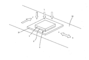
- FIG. 1 is a conceptual diagram illustrating an outline of laser lift-off processing according to an embodiment of the present invention.
- the laser lift-off process is performed as follows.
- a work 3 in which a material layer 2 is formed on a substrate 1 that transmits laser light is placed on a work stage 31.
- the work stage 31 on which the work 3 is placed is placed on a transport mechanism 32 such as a conveyor, and is transported by the transport mechanism 32 at a predetermined speed.
- the workpiece 3 is irradiated with a pulse laser beam L emitted from a pulse laser source (not shown) through the substrate 1 while being conveyed in the arrow AB direction in the figure together with the workpiece stage 31.
- the workpiece 3 is formed by forming a material layer 2 of a GaN (gallium nitride) compound on the surface of a substrate 1 made of sapphire.
- the substrate 1 may be any material as long as it can form a GaN-based compound material layer satisfactorily and transmits laser light having a wavelength necessary for decomposing the GaN-based compound material layer.
- a GaN-based compound is used for the material layer 2 in order to efficiently output high-output blue light with low input energy.
- the laser beam should be appropriately selected according to the substrate 1 and the substance constituting the material layer peeled from the substrate 1.
- a KrF (krypton fluorine) excimer laser that emits a wavelength of 248 nm can be used.
- the light energy (5 eV) with a laser wavelength of 248 nm is between the band gap of GaN (3.4 eV) and the band gap of sapphire (9.9 eV). Therefore, a laser beam having a wavelength of 248 nm is desirable for peeling the material layer of the GaN compound from the sapphire substrate.
- FIG. 2 is a diagram illustrating a state in which the laser beam L is applied to the workpiece 3.
- 2A shows a method of irradiating the workpiece 3 with the laser beam
- FIG. 2B shows an enlarged view of a portion X in FIG. 2A
- FIG. 2 shows an example of a cross-section of the light intensity distribution of laser light irradiated on each of the irradiation regions.
- the solid line on the workpiece 3 shown in FIG. 2 is merely a virtual representation of the laser light irradiation area.
- the workpiece 3 is repeatedly conveyed in the directions of arrows HA, HB, and HC shown in FIG.
- the laser beam L is applied from the back surface of the sapphire substrate 1 and is applied to the interface between the substrate 1 and the material layer 2.
- the shape of the laser beam L is formed into a substantially square shape.
- the workpiece 3 corresponds to the size of the workpiece itself, and the first conveyance operation HA is conveyed in the direction of arrow A in FIG. 1 and the irradiation region S of one shot of laser light.
- the second transport operation transported in the direction (in the direction of arrow C in FIG.
- the workpiece 3 has a circular outline, but the laser light irradiation area has a substantially rectangular shape, and a laser irradiation method for such a rectangular irradiation area will be described.
- the work 3 is conveyed in the HA direction of FIG. 2, while the end portions (edge portions) of the irradiation regions are superimposed on the four irradiation regions S 1, S 2, S 3, and S 4, respectively.
- the laser beam is irradiated once for a total of 4 times. This is the first transport operation.
- the workpiece 3 is transported in the HB direction in FIG.
- the laser beam is irradiated once for each of the six irradiation areas S5, S6, S7, S8, S9, and S10, once in total. To do.
- the laser light irradiation area moves relatively in the order of S1, S2, and S3.
- Each irradiation area is, for example, 0.5 mm ⁇ 0.5 mm, and the area is 0.25 mm. 2 .
- the area of the work 3 is 4560 mm 2 . That is, the laser light irradiation areas S1, S2, and S3 are much smaller than the work area.
- a laser beam in an irradiation area smaller than that of the workpiece 3 is irradiated to the workpiece 3 while scanning in the directions of arrows A and B shown in FIG.
- the laser optical system may be transported in accordance with the transport operations HA or HC described above while the workpiece is fixed.
- the laser beam may be irradiated to the workpiece so that the irradiation region of the laser beam on the workpiece changes with time.
- the end portions in the width direction of the pulsed laser light irradiated on the workpiece 3 overlap each other.
- the pulse laser beam irradiated to the workpiece 3 is irradiated in each of the irradiation areas S1 and S9, S2 and S8, S3 and S7, S4 and S6, which are adjacent to each other in the direction orthogonal to the conveyance direction HA of the workpiece 3.
- the width direction overlaps.
- the width of the overlapping region ST of the work 3 is, for example, 0.1 mm.
- the pulse interval of the laser beam is appropriately set in consideration of the workpiece conveyance speed and the width of the overlapping region ST of the laser beam irradiated on the adjacent irradiation regions S1, S2, S3. Basically, the pulse interval of the laser beam is determined so that the workpiece is not irradiated with the laser beam before the workpiece moves to the next irradiation region. That is, for example, the pulse interval of the laser beam is set shorter than the time required for the work to move a distance corresponding to the irradiation region for one shot of the laser beam. For example, when the conveying speed of the workpiece 3 is 100 mm / second and the width of the laser light overlapping region ST is 0.1 mm, the pulse interval of the laser light is 0.004 seconds (250 Hz).
- FIG. 3 is a conceptual diagram showing the configuration of the optical system of the laser lift-off device according to the embodiment of the present invention.
- a laser lift-off device 10 includes a laser source 20 that generates pulsed laser light, a laser optical system 40 for shaping the laser light into a predetermined shape, a work stage 31 on which the work 3 is placed, A transport mechanism 32 that transports the work stage 31 and a controller 33 that controls the irradiation interval of the laser light generated by the laser source 20 and the operation of the transport mechanism 32 are provided.
- the laser optical system 40 includes cylindrical lenses 41 and 42, a mirror 43 that reflects the laser light in the direction of the workpiece, a mask 44 for shaping the laser light into a predetermined shape, and the laser light L that has passed through the mask 44. And a projection lens 45 for projecting an image onto the work 3.
- the area and shape of the irradiation region of the pulse laser beam on the work 3 can be appropriately set by the laser optical system 40.
- a workpiece 3 is disposed at the tip of the laser optical system 40. The work 3 is placed on the work stage 31. The work stage 31 is placed on the transport mechanism 32 and is transported by the transport mechanism 32. Thereby, the workpiece
- the control unit 33 controls the pulse interval of the pulsed laser light generated by the laser source 20 so that the degree of superimposition of each laser light irradiated on the irradiation region adjacent to the workpiece 3 becomes a desired value.
- the laser light L generated from the laser source 20 is, for example, a KrF excimer laser that generates ultraviolet light having a wavelength of 248 nm.
- An ArF laser or a YAG laser may be used as the laser source.
- the light incident surface 3 ⁇ / b> A of the work 3 is disposed farther in the optical axis direction of the laser light than the focal point F of the projection lens 45.
- the light incident surface 3A of the workpiece 3 may be disposed closer to the projection lens 45 than the focal point F of the projection lens 45 in the optical axis direction of the laser light.
- a laser beam having a trapezoidal light intensity distribution as shown in FIG. 4 is obtained.
- the pulsed laser light L generated by the laser source 20 passes through the cylindrical lenses 41 and 42, the mirror 43, and the mask 44, and is then projected onto the work 3 by the projection lens 45.
- the pulse laser beam L is irradiated to the interface between the substrate 1 and the material layer 2 through the substrate 1 as shown in FIG.
- GaN near the interface between the material layer 2 and the substrate 1 is decomposed. In this way, the material layer 2 is peeled from the substrate 1.
- GaN in the material layer 2 is decomposed into Ga and N 2 .
- GaN decomposes a phenomenon as if it has exploded occurs, and the edge of the irradiation region of the pulse laser beam on the material layer 2 is damaged to some extent.
- the area and peripheral length of the irradiation region of the pulsed laser light applied to the material layer 2 are set to a predetermined relationship, whereby GaN is decomposed.
- the damage applied to the edge of the irradiation region of the pulse laser beam is reduced, and the occurrence of cracks in the material layer 2 is prevented.
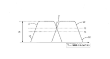
- FIG. 4 is a diagram showing the light intensity distribution of the laser light irradiated onto the workpiece 3 so as to overlap the regions S1 and S2 adjacent to each other of the workpiece 3 shown in FIG. 2, and aa ′ in FIG. It is line sectional drawing.
- the vertical axis indicates the intensity (energy value) of the laser beam irradiated to each irradiation area of the workpiece
- the horizontal axis indicates the conveyance direction of the workpiece.
- L1 and L2 indicate the profiles of the laser beams irradiated to the workpiece irradiation areas S1 and S2, respectively.
- the laser beams L1 and L2 are not irradiated at the same time, but the laser beam L2 is irradiated after one pulse interval from the irradiation of the laser beam L1.
- the cross sections of the laser beams L1 and L2 are formed in a substantially trapezoidal shape having a flat surface on the top (peak energy PE) following the edge portion LE that gently spreads in the circumferential direction.
- the laser beams L1 and L2 are superimposed in an energy region exceeding a decomposition threshold value VE necessary for decomposing and separating the material layer of the GaN-based compound from the sapphire substrate, as indicated by a broken line in FIG.
- the intensity (energy value) CE of the laser beam at the intersection position C between the laser beams L1 and L2 is set to a value exceeding the decomposition threshold value VE. This is because, as described above, when the irradiation region is shifted from S1 to S2 after irradiating the irradiation region S1 of FIG. 2 with the laser beam, the temperature of the region S1 is already lowered to the room temperature level.
- the irradiation amount of the pulse laser light irradiated to each of the irradiation regions S1 and S2 is not integrated.
- the intensity of the laser beam in the region where each laser beam is superimposed be VE ⁇ 1.15 or less with respect to the decomposition threshold VE necessary for peeling the material layer from the substrate.
- the superposition degree T the degree of superimposition T is 1 ⁇ T ⁇ 1.15.
- the pulse interval of the laser beam is adjusted in advance so that the laser beam applied to the adjacent irradiation region of the workpiece 3 is superimposed as described above with respect to the relative movement amount of the workpiece 3 and the laser beam.
- the decomposition threshold is 500 to 1500 J / cm 2 .
- the decomposition threshold VE needs to be set for each substance constituting the material layer.
- the laser beam intersecting in the energy region where the light intensity distributions of the laser beams L1 and L2 are below the decomposition threshold VE is used as a workpiece.
- an undecomposed region of GaN constituting the material layer was formed, and the material layer could not be sufficiently separated from the substrate.
- the undecomposed region of GaN coincided with the overlapping region ST where the laser beams L1 and L2 overlap on the workpiece.
- the workpiece is irradiated with the laser beam shown in the comparative example of FIG. 5B, the degree of superimposition T between the laser beams L1 and L2 is too large.
- the surface state of the material layer after peeling had many stains such as black spots on the surface. This is because the material layer once peeled off from the substrate is re-adhered by the second laser beam when the high-energy laser beam is irradiated twice at the same location, and the sapphire component constituting the substrate is It is thought that it adhered. Thus, the black spot formed on the surface of the material layer has an adverse effect on the light emission characteristics.
- the GaN material layer was formed on the sapphire substrate with the laser beams L1 and L2 (pulse laser beams output from the KrF laser) having the rectangular light intensity distribution shown in FIG.
- the surface of the material layer after peeling was examined by irradiating the workpiece.
- the intensity of the laser beam in the region where the laser beams L1 and L2 overlap is changed to 105%, 110%, 115%, and 120% with respect to the decomposition threshold VE (870 mJ / cm 2 ) of the GaN material layer. Irradiation was performed, and the surface of the material layer after peeling was examined.
- the intensity of the laser beam in the overlapping region is 105%, 110%, and 115 with respect to the decomposition threshold VE, respectively.
- % And 120% indicate the surface of the material layer after peeling.
- FIGS. 6 (b-1), (b-2), and (b-3) when the intensity of the laser beam in the overlapping region is 105%, 110%, and 115% with respect to the decomposition threshold VE In this case, the surface condition of the material layer after peeling was good, and no material that adversely affects the luminescent properties such as dirt and scratches was found.
- the intensity of the laser beam is set to 120% with respect to the decomposition threshold VE, as shown in FIG.
- the surface state of the material layer after peeling has many stains such as black spots. Been formed. From the above, by setting the laser energy in the range of VE ⁇ 1 to VE ⁇ 1.15 with respect to the decomposition threshold VE of GaN, the region of the GaN material layer including the region where the laser beam is superimposed is irradiated. It is considered that the laser lift-off process can be performed without damaging the surface.
- the material layer 2 is irradiated with pulsed laser light, whereby GaN in the material layer 2 is decomposed into Ga and N 2 .
- GaN decomposes a phenomenon appears as if it exploded, and damages the edge of the irradiated region of the pulsed laser light on the material layer 2. It is thought that it largely depends on the irradiation area.
- Table 1 shows the irradiation region shape (x, y), area (S), side length (L), S / L, stress applied to each side, and experimental evaluation results in the laser lift-off process.
- the shape of the irradiation region is rectangular, and in Table 1, x (mm) and y (mm) are the vertical and horizontal lengths of the irradiation region, and S (mm 2 ) is the area (xx) of the irradiation region. y) and L (mm) are the length of the periphery of the irradiated region (2x + 2y), and S / L is the ratio of the area S to the side length L.
- the stress (Pa) is 6000 atm (when the pressure of N 2 generated by the decomposition of GaN is calculated, the volume is 6000 times that of the atmospheric pressure because the volume is 6000 times).
- the strain stress is simulated and the maximum value of the strain stress distribution is obtained.
- the experimental evaluation results are obtained by examining the surface state of the material layer when the laser lift-off process is actually performed under the conditions shown in the table. In this experiment, a KrF laser that emits a laser beam having a wavelength of 248 nm was used, and the laser irradiation energy to the workpiece was set to VE ⁇ 1.1 with respect to the decomposition threshold value VE of the GaN material layer.
- the decomposition threshold of the GaN material layer is 870 J / cm 2 . Even when the laser energy is changed within the range of VE ⁇ 1 to VE ⁇ 1.15 with respect to the decomposition threshold VE of GaN, it is considered that a result similar to the result shown in Table 1 is obtained.
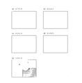
- FIG. 7 is a diagram schematically showing the result of this experiment.
- FIGS. Experimental results of 1, 4, 6, 7, and 9 are shown. In Table 1, No. The above experiment was not conducted for 2, 3 and 5.
- the laser lift-off process can be performed without causing damage by setting the area of the irradiation area to 0.25 mm 2 or less. It is considered a thing. However, if the irradiation area is a rectangle and the length of one side x is different from the length of the other side y, the value of [irradiation area S] / [peripheral length L of irradiation area] becomes small even if the area is the same. The upper limit value of the area of the irradiation region is larger than the above value. As shown in Table 1, no.
- the irradiation area of 3 is x0.1 mm and y7.0 mm (aspect ratio 70)
- the area of the irradiation area is 0.7 mm 2
- the stress value in this case is 8.36 ⁇ 10 8 Pa.
- No. No. 7 area is 0.25 mm 2 .
- the stress value of 7 was smaller than 1.53 ⁇ 10 9 Pa.
- the edge portion of the irradiation region It is considered that the force applied to the material layer can be reduced and the damage given to the material layer can be reduced.
- the shape of the irradiation area is limited in terms of the structure of the laser device, optical elements, etc., and it is difficult to form an extremely elongated irradiation area because the size of the laser device increases and the cost increases. is there.
- the irradiation distribution of the laser beam is preferably within ⁇ 5%, but it is difficult to satisfy such a requirement with an extremely long and narrow beam.
- the aspect ratio of the irradiation region is as described above. 70 or less.
- the shape of the irradiation region is preferably rectangular because the edge portions of adjacent irradiation regions need to be overlapped as described above, and the pulse to the workpiece 3 as shown in FIG.
- each laser light irradiation region (S1, S2, S3%) Has a shape close to a square shape
- the area of the irradiation region needs to be 0.25 mm 2 or less as described above, which is ideal. Is preferably 0.1 mm 2 or less.
- the shape of the irradiation region is a square shape, it is ideal if one side is preferably 0.3 mm or less.
- the beam shape (irradiation region shape) is not limited to a rectangle or a square, and may be a parallelogram, for example.
- a method for manufacturing a semiconductor light emitting device that can use the laser lift-off method described above will be described.
- the manufacturing method of the semiconductor light-emitting device formed of a GaN-based compound material layer will be described with reference to FIG.
- a sapphire substrate capable of crystal growth of a gallium nitride (GaN) compound semiconductor that transmits laser light and forms a material layer is used.
- GaN gallium nitride
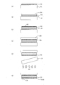
- FIG. 8A a GaN layer 102 made of a GaN-based compound semiconductor is rapidly formed on the sapphire substrate 101 by using, for example, a metal organic chemical vapor deposition method (MOCVD method). Subsequently, as illustrated in FIG.
- MOCVD method metal organic chemical vapor deposition method
- an n-type semiconductor layer 103 and a p-type semiconductor layer 104 that are light emitting layers are stacked on the surface of the GaN layer 102.
- GaN doped with silicon is used as the n-type semiconductor
- GaN doped with magnesium is used as the p-type semiconductor.
- solder 105 is applied on the p-type semiconductor layer 104.
- the support substrate 106 is attached on the solder 105.
- the support substrate 106 is made of, for example, an alloy of copper and tungsten. Then, as shown in FIG.
- the laser beam 107 is irradiated from the back surface side of the sapphire substrate 101 toward the interface between the sapphire substrate 101 and the GaN layer 102.
- the laser beam 107 is shaped so that the irradiation area is a square having an area of 0.25 mm 2 or less, and the light intensity distribution is substantially trapezoidal as shown in FIG.
- ITO 108 which is a transparent electrode is formed on the surface of the GaN layer 102 after peeling by vapor deposition, and the electrode 109 is attached to the surface of the ITO 108.
Landscapes
- Physics & Mathematics (AREA)
- Optics & Photonics (AREA)
- Engineering & Computer Science (AREA)
- Plasma & Fusion (AREA)
- Mechanical Engineering (AREA)
- Laser Beam Processing (AREA)
- Led Devices (AREA)
- Recrystallisation Techniques (AREA)
Abstract
Description
特に、小さい照射面積のパルスレーザ光を、基板を介して照射して、ワークへのパルスレーザ光の照射領域を刻々と変えながら、基板と結晶層の界面で結晶層を基板から剥離するレーザリフトオフ方法及びレーザリフトオフ装置に関するものである。
例えば、特許文献1においては、サファイア基板の上にGaN層を形成し、当該サファイア基板の裏面からレーザ光を照射することにより、GaN層を形成するGaNが分解され、当該GaN層をサファイア基板から剥離する技術について記載されている。以下では基板上に材料層が形成されたものをワークと呼ぶ。
ここで、レーザ光を照射した際には、GaNが分解することによりN2ガスが発生することから、当該GaN層にせん断応力が加わり、当該レーザ光の照射領域の境界部においてクラックが生じる場合がある。例えば、図9に示すように、レーザ光の1ショットの照射領域110が正方形状である場合、GaN層111のレーザ光の照射領域の境界112にクラックが発生してしまう問題がある。
特に、数μm以下の厚みのGaN系化合物材料層を用いて素子を形成する場合には、GaN系化合物材料層がN2ガス発生によるせん断応力に耐えるための十分な強度を有しない場合もあり、容易にクラックが発生してしまう。更に、GaN系化合物材料層のみならず、その上に形成された発光層などにクラックが伝播し、素子そのものが破壊されてしまう場合もあり、微小なサイズの素子を形成する際の問題となっている。
本発明は、上記した問題点を解決するものであって、本発明の目的は、基板上に形成された材料層に割れを生じさせることなく、当該基板から当該材料層を剥離することができるレーザリフトオフ方法および装置を提供することである。
すなわち、[照射面積S]/[周囲長L]の値を小さくすることでダメージを小さくできるものと考えられ、具体的には、上記S/Lの値を0.125以下とすることにより、ダメージを与えることなく、レーザリフトオフ処理を行うことができることを見出した。
以上に基づき、本発明においては、次のように前記課題を解決する。
(1)基板上に結晶層が形成されてなるワークに対し、前記基板を通してパルスレーザ光を照射して、前記ワークへのパルスレーザ光の照射領域を刻々と変えながら、前記基板と前記結晶層との界面で前記結晶層を前記基板から剥離するレーザリフトオフ方法において、前記ワークへのパルスレーザ光の照射領域を、該照射領域の面積をS(mm2)、照射領域の周囲長をL(mm)としたとき、S/L≦0.125の関係を満たすように設定する。
(2)上記(1)において、ワークへのパルスレーザ光の照射領域を四角形とする。
(3)基板上に結晶層が形成されてなるワークに対し、前記基板を通してパルスレーザ光を照射して、前記ワークへのパルスレーザ光の照射領域を刻々と変えながら、前記基板と前記結晶層との界面で前記結晶層を前記基板から剥離するレーザリフトオフ装置において、前記基板を透過すると共に前記結晶層を分解するために必要な波長域のパルスレーザ光を発生するレーザ源と、前記ワークを搬送する搬送機構と、前記レーザ源から発したパルスレーザ光を、前記ワークへのパルスレーザ光の照射領域の面積をS(mm2)、照射領域の周囲長をL(mm)としたとき、S/L≦0.125の関係になるように成形するレーザ光学系とを設ける。
(4)上記(3)において、前記レーザ光学系が、前記ワークへのパルスレーザ光の照射領域を四角形に成形する。
(1)ワークへのパルスレーザ光の照射領域を、該照射領域の面積をS(mm2)、照射領域の周囲長をL(mm)としたとき、S/L≦0.125の関係を満たすように設定することにより、パルスレーザ光の照射領域のエッジ部に加わるダメージを軽減することができ、材料層へのクラック発生を防止することができる。
(2)照射領域を四角形とすることで、照射領域のエッジ部を重畳させながらワークの全面にレーザ光を照射することができ、材料層にクラックを発生させることなく、ワーク全面に対してレーザリフトオフ処理を行うことができる。
同図に示すように、本実施例において、レーザリフトオフ処理は次のように行われる。
レーザ光を透過する基板1上に材料層2が形成されたワーク3が、ワークステージ31上に載置されている。ワーク3を載せたワークステージ31は、コンベヤのような搬送機構32に載置され、搬送機構32によって所定の速度で搬送される。ワーク3は、ワークステージ31と共に図中の矢印AB方向に搬送されながら、基板1を通じて、図示しないパルスレーザ源から出射するパルスレーザ光Lが照射される。
ワーク3は、サファイアからなる基板1の表面に、GaN(窒化ガリウム)系化合物の材料層2が形成されてなるものである。基板1は、GaN系化合物の材料層を良好に形成することができ、尚且つ、GaN系化合物材料層を分解するために必要な波長のレーザ光を透過するものであれば良い。材料層2には、低い入力エネルギーによって高出力の青色光を効率良く出力するためにGaN系化合物が用いられる。
図2(a)はワーク3に対するレーザ光の照射方法を示し、図2(b)は図2(a)のX部を拡大して示したものであり、図2(b)では、ワーク3の各照射領域の照射されるレーザ光の光強度分布の断面の一例を示している。なお、図2に示すワーク3上の実線は、レーザ光の照射領域を仮想的に示すものに過ぎない。
ワーク3は、搬送機構32によって図2に示す矢印HA、HB、HCの方向に繰返し搬送される。レーザ光Lはサファイアの基板1の裏面から照射され、基板1と材料層2の界面に照射される。レーザ光Lの形状は略方形状に成形される。
ワーク3は、図1、2に示すように、ワーク自体のサイズに対応して、図1の矢印Aの方向に搬送される第1の搬送動作HAと、レーザ光の1ショットの照射領域Sに相当する距離から、照射領域が重畳する重畳領域STを差し引いた距離だけ第1の搬送動作HAの搬送方向と直交する方向(図1の矢印Cの方向)に搬送される第2の搬送動作HBと、図1の矢印Bの方向に搬送される第3の搬送動作HCとが順次に実行される。第1の搬送動作HAおよび第3の搬送動作HCのそれぞれの搬送方向は180°異なっている。
ここで、レーザ光の光学系は固定されたままであり搬送されない。つまり、レーザ光の光学系を固定した状態でワーク3のみが搬送されることによって、ワーク3におけるレーザ光Lの照射領域が、図2の矢印に示すようにS1,…S10,…の順に相対的に刻々と変わることになる。
図2に示すように、ワーク3を図2のHA方向に搬送し、S1、S2、S3、S4の4つの照射領域に対して、照射領域の端部(エッジ部)を重畳させながら、それぞれ1回ずつ合計4回に亘りレーザ光を照射する。これが第1の搬送動作である。
次に、レーザ光がワーク3の次なる照射領域S5に照射されるようにするため、ワーク3を図2のHB方向に搬送する。これが第2の搬送動作である。ワーク3が矢印HB方向に搬送される距離は、パルスレーザ光の1ショット(1パルス)分の照射領域に相当する距離から重畳領域STを差し引いた距離に等しい。
その次に、ワーク3を図2のHC方向に搬送させながら、S5,S6、S7、S8、S9、S10の6つの照射領域に対して、それぞれ1回ずつ合計6回に亘りレーザ光を照射する。これが第3の搬送動作である。ワーク3のその他の照射領域についても上記の一連の手順に従ってワーク3を搬送することにより、ワーク3の全域に亘りレーザ光が照射される。
本実施例のレーザリフトオフ処理では、ワーク3に比して小さい照射領域のレーザ光が図1に示す矢印AおよびBの方向(つまりワークの左右方向)にスキャンしながらワーク3に対して照射される。なお、本発明の実施例とは逆に、ワークを固定したままで、上記した搬送動作HAないしHCに従ってレーザの光学系を搬送しても良い。要は、ワーク上のレーザ光の照射領域が時間とともに刻々と移り変わるように、ワークに対してレーザ光が照射されれば良い。
レーザ光のパルス間隔は、ワークの搬送速度と、ワーク3上の隣接する照射領域S1、S2、S3・・・に照射されるレーザ光の重畳領域STの幅を考慮して適宜設定される。
基本的にはワークが次なる照射領域に移動する前にレーザ光がワークに照射されることのないように、レーザ光のパルス間隔が決められる。つまり、例えばレーザ光のパルス間隔は、ワークがレーザ光の1ショット分の照射領域に相当する距離を移動するために要する時間よりも短く設定される。例えば、ワーク3の搬送速度が100mm/秒、レーザ光の重畳領域STの幅が0.1mmである場合、レーザ光のパルス間隔は0.004秒(250Hz)である。
レーザ光学系40は、シリンドリカルレンズ41、42と、レーザ光をワークの方向へ反射するミラー43と、レーザ光を所定の形状に成形するためのマスク44と、マスク44を通過したレーザ光Lの像をワーク3上に投影する投影レンズ45とを備えている。ワーク3へのパルスレーザ光の照射領域の面積および形状は、レーザ光学系40によって適宜設定することができる。
レーザ光学系40の先にはワーク3が配置されている。ワーク3はワークステージ31上に載置されている。ワークステージ31は搬送機構32に載置されており、搬送機構32によって搬送される。これにより、ワーク3が、図1に示す矢印A、Bの方向に順次に搬送され、ワーク3におけるレーザ光の照射領域が刻々と変わる。制御部33は、ワーク3の隣接する照射領域に照射される各レーザ光の重畳度が所望の値になるように、レーザ源20で発生するパルスレーザ光のパルス間隔を制御する。
レーザ源20で発生したパルスレーザ光Lは、シリンドリカルレンズ41、42、ミラー43、マスク44を通過した後に、投影レンズ45によってワーク3上に投影される。パルスレーザ光Lは、図1に示したように基板1を通じて基板1と材料層2の界面に照射される。基板1と材料層2の界面では、パルスレーザ光Lが照射されることにより、材料層2の基板1との界面付近のGaNが分解される。このようにして材料層2が基板1から剥離される。
本発明のレーザリフトオフ処理においては、後述するように、材料層2に照射されるパルスレーザ光の照射領域の面積と周囲長を所定の関係に設定しており、これにより、GaNが分解するときにパルスレーザ光の照射領域のエッジ部に加わるダメージを軽減し、材料層2へのクラック発生を防止している。
同図において縦軸はワークの各照射領域に照射されるレーザ光の強度(エネルギー値)を、横軸はワークの搬送方向を示す。また、L1、L2は、それぞれワークの照射領域S1、S2に照射されるレーザ光のプロファイルを示す。なお、レーザ光L1,L2は同時に照射されるわけではなく、レーザ光L1が照射されてから1パルス間隔後にレーザ光L2が照射される。
この例では、図4に示すように、レーザ光L1、L2の断面は、周方向になだらかに広がるエッジ部LEに続いて頂上(ピークエネルギーPE)に平坦面を有する略台形状に形成されている。そして、レーザ光L1、L2は、図4に破線で示すように、GaN系化合物の材料層を分解してサファイアの基板から剥離させるために必要な分解閾値VEを超えるエネルギー領域において重畳される。
これは、前述したように、図2の照射領域S1にレーザ光を照射した後に照射領域をS1からS2に移行させたとき、領域S1の温度は既に室温レベルまで低下した状態となるため、照射領域S1の温度が室温レベルに低下した状態で照射領域S2にレーザ光を照射したとしても、それぞれの照射領域S1、S2に照射されるパルスレーザ光の照射量が積算されないためである。
レーザ光L1とL2との交差位置Cでのレーザ光の強度CE、すなわち、レーザ光が重畳して照射される領域におけるそれぞれのパルスレーザ光の強度を、上記分解閾値VEを越える値になるように設定することで、材料層を基板から剥離させるために十分なレーザエネルギーが与えることができ、基板上に形成された材料層に割れを生じさせることなく、材料層を基板から確実に剥離させることができる。
これは、同じ領域に、強度が大きなパルスレーザ光が2度照射されることにより、一度基板から剥離した材料層が、2度目に照射されるパルスレーザ光により再接着するものと考えられる。
実験等により、各レーザ光が重畳している領域におけるレーザ光の強度は、前記材料層を前記基板から剥離させるに必要な分解閾値VEに対して、VE×1.15以下にするのが望ましいことが分かった。
すなわち、[レーザ光が重畳している領域におけるレーザ光の強度(最大値)]/[分解閾値VE]を重畳度Tと定義すると、基板上に形成された材料層に割れを生じさせることなく、かつ基板を再接着させることなく、材料層を基板から確実に剥離させるためには、重畳度Tを1≦T≦1.15とするのが望ましい。
なお、ワーク3とレーザ光の相対的な移動量に対して、レーザ光のパルス間隔は、ワーク3の隣接する照射領域に照射されるレーザ光が前記のように重畳するように予め調整されている。同図に示す実施例では、材料層がGaNであるため、分解閾値は500~1500J/cm2である。分解閾値VEは、材料層を構成する物質毎に設定することが必要とされる。
一方、図5(b)の比較例に示すレーザ光をワークに照射した場合は、レーザ光L1とL2との重畳度Tが大きすぎるため、後述する実験結果の図6(b-4)に示すように、剥離後の材料層の表面状態は、表面に黒いシミのような汚れが多数形成された。
これは、エネルギーが大きなレーザ光が同じ個所に2度照射されることにより、一度基板から剥離した材料層が、2度目に照射されるレーザ光により再接着し、基板を構成するサファイアの成分が付着したものと考えられる。このように材料層の表面に形成された黒いシミは発光特性に悪影響を及ぼす。
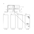
実験では、レーザ光L1,L2が重畳する領域でのレーザ光の強度を、GaN材料層の分解閾値VE(870mJ/cm2)に対して105%、110%、115%、120%と変えて照射し、剥離後の材料層の表面を調べた。
図6(b-1)、(b-2)(b-3)、(b-4)に、重畳する領域におけるレーザ光の強度を分解閾値VEに対して、それぞれ105%、110%、115%、120%と変えた場合の剥離後の材料層の表面を示す。
図6(b-1)、(b-2)(b-3)に示すように、分解閾値VEに対して、重畳する領域でのレーザ光の強度が105%、110%、115%の場合には、剥離後の材料層の表面状態は良好であり、汚れ、傷などといった発光特性に悪影響を与えるものは見あたらなかった。これに対し、レーザ光の強度を分解閾値VEに対して120%にすると、図6(b-4)に示すように、剥離後の材料層の表面状態は、黒いシミのような汚れが多数形成された。
以上のことから、レーザエネルギーをGaNの分解閾値VEに対してVE×1~VE×1.15の範囲とすることで、レーザ光が重畳して照射される領域を含めて、GaN材料層の表面にダメージを与えことなく、レーザリフトオフ処理を行うことができるものと考えられる。
前述したように、材料層2はパルスレーザ光が照射されることにより、材料層2のGaNがGaとN2とに分解する。GaNが分解するときは、あたかも爆発したような現象が生じ、材料層2へのパルスレーザ光の照射領域のエッジ部に対してダメージを与えるが、この分解によるダメージの大きさは、レーザ光の照射面積に大きく依存しているものと考えられる。すなわち、照射面積Sが大きいほど、上記N2ガスの発生量が多くなる等、パルスレーザ光の照射領域のエッジ部へ大きな力が加わるものと考えられる。一方、エッジ部の長さ(照射領域の周囲長)Lが大きくなれば、上記エッジ部に加わる力が大きくなっても、単位長さ当たりに加わる力は小さくなり、照射面積が同じであっても、ダメージは小さくなる。
ここでは、照射領域の形状は矩形状としており、表1において、x(mm),y(mm)は照射領域の縦、横の長さ、S(mm2)は照射領域の面積(x×y)、L(mm)は照射領域の周囲の長さ(2x+2y)、S/Lは面積Sと辺の長さLの比である。また、応力(Pa)は、GaNの分解により発生するN2の圧力を計算すると6000気圧(体積が6000倍になるため、大気圧の6000倍の圧力になる)であり、この圧力によるGaNに対する歪み応力をシュミレーションし、歪み応力分布のうちの最大値を求めたものである。
また、実験での評価結果は、表に示される条件で実際にレーザリフトオフ処理を行ったときの材料層の表面状態を調べたものである。
この実験は、波長248nmのレーザ光を出射するKrFレーザを用い、ワークへのレーザの照射エネルギーはGaN材料層の分解閾値VEに対してVE×1.1とした。なお、GaN材料層の分解閾値は870J/cm2である。
なお、レーザエネルギーをGaNの分解閾値VEに対してVE×1~VE×1.15の範囲で変えた場合でも、上記表1に示す結果と同様な結果が得られるものと考えられる。
図7はこの実験結果を模式的に示した図であり、同図(a)~(e)はそれぞれ表1のNo.1,4,6,7,9の実験結果を示している。なお、表1のNo.2,3,5について上記実験は行っていない。

以上の結果から、S/Lが0.125以下であれば、応力値は1.53×109Pa以下になり、ダメージの発生はないと考えられる。一方、S/Lが上記値を超えると、剥離後の材料層にダメージを与えるものと考える。
すなわち、照射領域の面積S/周囲長Lの値を0.125以下とすることにより、ダメージを与えることなく、レーザリフトオフ処理を行うことができるものと考える。
表1に示すように、No.3の照射領域がx0.1mm、y7.0mm(縦横比70)の場合の照射領域の面積は、0.7mm2であり、この場合の応力値は8.36×10⁸Paとなり、照射領域の面積が上記No.7(面積が0.25mm2)より大きいにもかかわらず、No.7の応力値1.53×10⁹Paより小さくなった。
すなわち、照射領域の面積がダメージの発生に大きな影響を与えるものの、[照射面積S]/[照射領域の周囲長L]が0.125以下となるように設定することで、照射領域のエッジ部へ加わる力を小さくし、材料層に与えるダメージを小さくすることができるものと考えられる。
なお、上記照射領域の形状は、前記したように隣り合う照射領域のエッジ部を重畳させる必要があることから、矩形状であることが望ましく、前記図2に示したようにワーク3へのパルスレーザ光の各照射領域(S1、S2、S3・・・)を正方形状に近い形状にする場合、照射領域の面積は上記したように0.25mm2以下であることが必要であり、理想的には0.1mm2以下であることが望ましい。また、照射領域の形状が正方形状の場合は、好ましくは1辺が0.3mm以下であれば理想的である。なお、ビーム形状(照射領域の形状)は長方形や正方形に限定されず、例えば平行四辺形であってもよい。
結晶成長用の基板には、レーザ光を透過し材料層を構成する窒化ガリウム(GaN)系化合物半導体を結晶成長させることができるサファイア基板を使用する。図8(a)に示すように、サファイア基板101上には、例えば有機金属気相成長法(MOCVD法)を用いて迅速にGaN系化合物半導体よりなるGaN層102が形成される。
続いて、図8(b)に示すように、GaN層102の表面には、発光層であるn型半導体層103とp型半導体層104とを積層させる。例えば、n型半導体としてはシリコンがドープされたGaNが用いられ、p型半導体としてはマグネシウムがドープされたGaNが用いられる。
続いて、図8(c)に示すように、p型半導体層104上には、半田105が塗布される。続いて、図8(d)に示すように、半田105上にサポート基板106が取付けられる。サポート基板106は例えば銅とタングステンの合金からなる。
そして、図8(e)に示すように、サファイア基板101の裏面側からサファイア基板101とGaN層102との界面に向けてレーザ光107を照射する。レーザ光107は、照射領域が0.25mm2以下の面積を有する正方形となり、かつ、光強度分布が図4に示したような略台形状となるように成形される。
レーザ光107をサファイア基板101とGaN層102の界面に照射して、GaN層102を分解することにより、サファイア基板101からGaN層102を剥離する。剥離後のGaN層102の表面に透明電極であるITO108を蒸着により形成し、ITO108の表面に電極109を取付ける。
2 材料層
3 ワーク
10 レーザリフトオフ装置
20 レーザ源
31 ワークステージ
32 搬送機構
33 制御部
40 レーザ光学系
41、42 シリンドリカルレンズ
43 ミラー
44 マスク
45 投影レンズ
101 サファイア基板
102 GaN層
103 n型半導体層
104 p型半導体層
105 半田
106 サポート基板
107 レーザ光
108 透明電極(ITO)
109 電極
L レーザ光
Claims (4)
- 基板上に結晶層が形成されてなるワークに対し、前記基板を通してパルスレーザ光を照射して、前記ワークへのパルスレーザ光の照射領域を刻々と変えながら、前記基板と前記結晶層との界面で前記結晶層を前記基板から剥離するレーザリフトオフ方法において、
前記ワークへのパルスレーザ光の照射領域を、該照射領域の面積をS(mm2)、照射領域の周囲長をL(mm)としたとき、S/L≦0.125の関係を満たすように設定することを特徴とするレーザリフトオフ方法。 - 前記ワークへのパルスレーザ光の照射領域が四角形である
ことを特徴とする請求項1記載のレーザリフトオフ方法。 - 基板上に結晶層が形成されてなるワークに対し、前記基板を通してパルスレーザ光を照射して、前記ワークへのパルスレーザ光の照射領域を刻々と変えながら、前記基板と前記結晶層との界面で前記結晶層を前記基板から剥離するレーザリフトオフ装置において、
前記基板を透過すると共に前記結晶層を分解するために必要な波長域のパルスレーザ光を発生するレーザ源と、
前記ワークを搬送する搬送機構と、
前記レーザ源から発したパルスレーザ光を、前記ワークへのパルスレーザ光の照射領域の面積をS(mm2)、照射領域の周囲長をL(mm)としたとき、S/L≦0.125の関係になるように成形するレーザ光学系とを備える
ことを特徴とするレーザリフトオフ装置。 - 前記レーザ光学系は、前記ワークへのパルスレーザ光の照射領域を四角形に成形することを特徴とする請求項3記載のレーザリフトオフ装置。
Priority Applications (3)
| Application Number | Priority Date | Filing Date | Title |
|---|---|---|---|
| CN201080067951.0A CN102986001B (zh) | 2010-07-20 | 2010-09-28 | 激光剥离方法以及激光剥离装置 |
| US13/811,094 US20130119031A1 (en) | 2010-07-20 | 2010-09-28 | Laser lift-off method and laser lift-off apparatus |
| KR1020137003130A KR101362633B1 (ko) | 2010-07-20 | 2010-09-28 | 레이저 리프트 오프 방법 및 레이저 리프트 오프 장치 |
Applications Claiming Priority (2)
| Application Number | Priority Date | Filing Date | Title |
|---|---|---|---|
| JP2010163273A JP4948629B2 (ja) | 2010-07-20 | 2010-07-20 | レーザリフトオフ方法 |
| JP2010-163273 | 2010-07-20 |
Publications (1)
| Publication Number | Publication Date |
|---|---|
| WO2012011202A1 true WO2012011202A1 (ja) | 2012-01-26 |
Family
ID=45496642
Family Applications (1)
| Application Number | Title | Priority Date | Filing Date |
|---|---|---|---|
| PCT/JP2010/066792 Ceased WO2012011202A1 (ja) | 2010-07-20 | 2010-09-28 | レーザリフトオフ方法及びレーザリフトオフ装置 |
Country Status (6)
| Country | Link |
|---|---|
| US (1) | US20130119031A1 (ja) |
| JP (1) | JP4948629B2 (ja) |
| KR (1) | KR101362633B1 (ja) |
| CN (1) | CN102986001B (ja) |
| TW (1) | TWI417159B (ja) |
| WO (1) | WO2012011202A1 (ja) |
Cited By (2)
| Publication number | Priority date | Publication date | Assignee | Title |
|---|---|---|---|---|
| US10350710B2 (en) | 2015-04-08 | 2019-07-16 | The Japan Steel Works, Ltd. | Laser irradiation method and apparatus |
| KR20230050312A (ko) | 2020-08-18 | 2023-04-14 | 닛토덴코 가부시키가이샤 | 부재 전사 방법 |
Families Citing this family (16)
| Publication number | Priority date | Publication date | Assignee | Title |
|---|---|---|---|---|
| US8986497B2 (en) | 2009-12-07 | 2015-03-24 | Ipg Photonics Corporation | Laser lift off systems and methods |
| US9669613B2 (en) * | 2010-12-07 | 2017-06-06 | Ipg Photonics Corporation | Laser lift off systems and methods that overlap irradiation zones to provide multiple pulses of laser irradiation per location at an interface between layers to be separated |
| JP5996250B2 (ja) * | 2012-04-24 | 2016-09-21 | 株式会社ディスコ | リフトオフ方法 |
| JP6072541B2 (ja) * | 2013-01-04 | 2017-02-01 | スタンレー電気株式会社 | 窒化物半導体素子の製造方法 |
| JP2015002239A (ja) * | 2013-06-14 | 2015-01-05 | シャープ株式会社 | 窒化物半導体発光素子および窒化物半導体発光素子の製造方法 |
| KR101794828B1 (ko) * | 2013-08-28 | 2017-11-09 | 에이피시스템 주식회사 | 막 분리 장치 |
| DE102014213775B4 (de) * | 2014-07-15 | 2018-02-15 | Innolas Solutions Gmbh | Verfahren und Vorrichtung zum laserbasierten Bearbeiten von flächigen, kristallinen Substraten, insbesondere von Halbleitersubstraten |
| CN107452898B (zh) * | 2016-05-31 | 2019-08-23 | 上海微电子装备(集团)股份有限公司 | 一种激光剥离装置和方法 |
| KR102480839B1 (ko) * | 2016-07-05 | 2022-12-26 | 삼성디스플레이 주식회사 | 레이저 결정화 장치 및 이의 구동 방법 |
| CN107452842A (zh) * | 2017-09-15 | 2017-12-08 | 西安交通大学 | 采用减反膜降低垂直结构深紫外led激光剥离能量阈值的方法 |
| WO2019220666A1 (ja) * | 2018-05-17 | 2019-11-21 | 信越エンジニアリング株式会社 | ワーク分離装置及びワーク分離方法 |
| US10840141B2 (en) | 2018-06-18 | 2020-11-17 | Shin-Etsu Engineering Co., Ltd. | Workpiece-separating device and workpiece-separating method |
| JP7280697B2 (ja) * | 2019-01-09 | 2023-05-24 | 太陽誘電株式会社 | 積層セラミックコンデンサの製造方法 |
| TWI836077B (zh) | 2019-05-22 | 2024-03-21 | 日商力森諾科股份有限公司 | 半導體裝置的製造方法 |
| CN114641846B (zh) | 2019-11-20 | 2023-03-24 | 信越工程株式会社 | 工件分离装置及工件分离方法 |
| KR102432964B1 (ko) * | 2020-11-16 | 2022-08-18 | (주)티티에스 | 레이저 빔의 중첩을 통한 부품 표면 재생 장치 |
Citations (4)
| Publication number | Priority date | Publication date | Assignee | Title |
|---|---|---|---|---|
| JP2001501778A (ja) * | 1996-10-01 | 2001-02-06 | シーメンス アクチエンゲゼルシヤフト | 2つの材料層を相互に分離する方法及びこの方法により製造された電子部品 |
| JP2003168820A (ja) * | 2001-12-03 | 2003-06-13 | Sony Corp | 剥離方法、レーザー光の照射方法及びこれらを用いた素子の製造方法 |
| JP2007149988A (ja) * | 2005-11-28 | 2007-06-14 | Tokyo Institute Of Technology | レーザーリフトオフ法およびレーザーリフトオフ装置 |
| JP2007534164A (ja) * | 2004-03-29 | 2007-11-22 | ジェイピー・サーセル・アソシエイツ・インコーポレーテッド | 材料層の分離方法 |
Family Cites Families (28)
| Publication number | Priority date | Publication date | Assignee | Title |
|---|---|---|---|---|
| NL260906A (ja) * | 1960-02-12 | |||
| US4155779A (en) * | 1978-08-21 | 1979-05-22 | Bell Telephone Laboratories, Incorporated | Control techniques for annealing semiconductors |
| JPS5861622A (ja) * | 1981-10-09 | 1983-04-12 | Hitachi Ltd | 単結晶薄膜の製造方法 |
| FR2542327B1 (ja) * | 1983-03-07 | 1986-03-07 | Bensoussan Marcel | |
| US4670063A (en) * | 1985-04-10 | 1987-06-02 | Eaton Corporation | Semiconductor processing technique with differentially fluxed radiation at incremental thicknesses |
| DE3514824A1 (de) * | 1985-04-24 | 1986-11-06 | Siemens Ag | Verfahren zur bildung von schmalen, metallfreien streifen in der metallschicht von kunststoffolien |
| FR2681472B1 (fr) * | 1991-09-18 | 1993-10-29 | Commissariat Energie Atomique | Procede de fabrication de films minces de materiau semiconducteur. |
| US6534380B1 (en) * | 1997-07-18 | 2003-03-18 | Denso Corporation | Semiconductor substrate and method of manufacturing the same |
| US6686623B2 (en) * | 1997-11-18 | 2004-02-03 | Semiconductor Energy Laboratory Co., Ltd. | Nonvolatile memory and electronic apparatus |
| AU2514900A (en) * | 1999-01-27 | 2000-08-18 | United States Of America As Represented By The Secretary Of The Navy, The | Fabrication of conductive/non-conductive nanocomposites by laser evaporation |
| JP4084039B2 (ja) * | 2001-11-19 | 2008-04-30 | 株式会社 液晶先端技術開発センター | 薄膜半導体装置及びその製造方法 |
| US7119365B2 (en) * | 2002-03-26 | 2006-10-10 | Sharp Kabushiki Kaisha | Semiconductor device and manufacturing method thereof, SOI substrate and display device using the same, and manufacturing method of the SOI substrate |
| US7508034B2 (en) * | 2002-09-25 | 2009-03-24 | Sharp Kabushiki Kaisha | Single-crystal silicon substrate, SOI substrate, semiconductor device, display device, and manufacturing method of semiconductor device |
| US20040140296A1 (en) * | 2003-01-22 | 2004-07-22 | Lis Steven A. | Close proximity pulsed laser catalyst deposition system and method |
| JP4662918B2 (ja) * | 2003-01-31 | 2011-03-30 | オスラム オプト セミコンダクターズ ゲゼルシャフト ミット ベシュレンクテル ハフツング | 半導体構成素子の製造のための方法 |
| US7341628B2 (en) * | 2003-12-19 | 2008-03-11 | Melas Andreas A | Method to reduce crystal defects particularly in group III-nitride layers and substrates |
| JP2007142001A (ja) * | 2005-11-16 | 2007-06-07 | Denso Corp | レーザ加工装置およびレーザ加工方法 |
| JP2007307599A (ja) * | 2006-05-20 | 2007-11-29 | Sumitomo Electric Ind Ltd | スルーホール成形体およびレーザー加工方法 |
| DE102006046363B4 (de) * | 2006-09-29 | 2009-04-16 | Advanced Micro Devices, Inc., Sunnyvale | Verfahren zum Verringern von Kristalldefekten in Transistoren mit wieder aufgewachsenen flachen Übergängen durch geeignetes Auswählen von Kristallorientierungen |
| JP2008147406A (ja) * | 2006-12-08 | 2008-06-26 | Cyber Laser Kk | レーザによる集積回路の修正方法および装置 |
| KR101499175B1 (ko) * | 2007-10-04 | 2015-03-05 | 가부시키가이샤 한도오따이 에네루기 켄큐쇼 | 반도체 기판의 제조방법 |
| CN101740331B (zh) * | 2008-11-07 | 2012-01-25 | 东莞市中镓半导体科技有限公司 | 利用固体激光器无损剥离GaN与蓝宝石衬底的方法 |
| DE102009044038A1 (de) * | 2009-09-17 | 2011-03-31 | Schott Solar Ag | Verfahren zur Herstellung eines Kontaktbereichs eines elektronischen Bauteils |
| US8026521B1 (en) * | 2010-10-11 | 2011-09-27 | Monolithic 3D Inc. | Semiconductor device and structure |
| CN102792420B (zh) * | 2010-03-05 | 2016-05-04 | 并木精密宝石株式会社 | 单晶衬底、单晶衬底的制造方法、带多层膜的单晶衬底的制造方法以及元件制造方法 |
| JP4661989B1 (ja) * | 2010-08-04 | 2011-03-30 | ウシオ電機株式会社 | レーザリフトオフ装置 |
| US8365398B2 (en) * | 2011-01-26 | 2013-02-05 | Jeng-Jye Shau | Accurate alignment for stacked substrates |
| JP5909854B2 (ja) * | 2011-03-01 | 2016-04-27 | ウシオ電機株式会社 | レーザリフトオフ装置およびレーザリフトオフ方法 |
-
2010
- 2010-07-20 JP JP2010163273A patent/JP4948629B2/ja not_active Expired - Fee Related
- 2010-09-28 KR KR1020137003130A patent/KR101362633B1/ko not_active Expired - Fee Related
- 2010-09-28 CN CN201080067951.0A patent/CN102986001B/zh not_active Expired - Fee Related
- 2010-09-28 WO PCT/JP2010/066792 patent/WO2012011202A1/ja not_active Ceased
- 2010-09-28 US US13/811,094 patent/US20130119031A1/en not_active Abandoned
- 2010-10-27 TW TW099136710A patent/TWI417159B/zh not_active IP Right Cessation
Patent Citations (4)
| Publication number | Priority date | Publication date | Assignee | Title |
|---|---|---|---|---|
| JP2001501778A (ja) * | 1996-10-01 | 2001-02-06 | シーメンス アクチエンゲゼルシヤフト | 2つの材料層を相互に分離する方法及びこの方法により製造された電子部品 |
| JP2003168820A (ja) * | 2001-12-03 | 2003-06-13 | Sony Corp | 剥離方法、レーザー光の照射方法及びこれらを用いた素子の製造方法 |
| JP2007534164A (ja) * | 2004-03-29 | 2007-11-22 | ジェイピー・サーセル・アソシエイツ・インコーポレーテッド | 材料層の分離方法 |
| JP2007149988A (ja) * | 2005-11-28 | 2007-06-14 | Tokyo Institute Of Technology | レーザーリフトオフ法およびレーザーリフトオフ装置 |
Cited By (2)
| Publication number | Priority date | Publication date | Assignee | Title |
|---|---|---|---|---|
| US10350710B2 (en) | 2015-04-08 | 2019-07-16 | The Japan Steel Works, Ltd. | Laser irradiation method and apparatus |
| KR20230050312A (ko) | 2020-08-18 | 2023-04-14 | 닛토덴코 가부시키가이샤 | 부재 전사 방법 |
Also Published As
| Publication number | Publication date |
|---|---|
| TW201204498A (en) | 2012-02-01 |
| KR101362633B1 (ko) | 2014-02-12 |
| US20130119031A1 (en) | 2013-05-16 |
| CN102986001B (zh) | 2014-09-24 |
| TWI417159B (zh) | 2013-12-01 |
| KR20130036317A (ko) | 2013-04-11 |
| JP4948629B2 (ja) | 2012-06-06 |
| CN102986001A (zh) | 2013-03-20 |
| JP2012024783A (ja) | 2012-02-09 |
Similar Documents
| Publication | Publication Date | Title |
|---|---|---|
| JP4948629B2 (ja) | レーザリフトオフ方法 | |
| EP1735837B1 (en) | Method of separating layers of material | |
| JP5712700B2 (ja) | レーザリフトオフ装置 | |
| WO2012002155A1 (ja) | レーザリフトオフ方法及びレーザリフトオフ装置 | |
| JP6390898B2 (ja) | 基板の製造方法、加工対象物の切断方法、及び、レーザ加工装置 | |
| JP5073915B2 (ja) | 半導体素子の製造方法 | |
| KR101254639B1 (ko) | 반도체 발광 소자의 제조 방법 | |
| CN102986005B (zh) | 激光剥离装置 | |
| US20100151602A1 (en) | Laser roughening to improve led emissions | |
| JP5240318B2 (ja) | レーザリフトオフ方法 | |
| WO2012046478A1 (ja) | レーザリフトオフ方法及びレーザリフトオフ装置 | |
| JP2012080020A (ja) | レーザリフトオフ方法及びレーザリフトオフ装置 | |
| JP2012146771A (ja) | レーザリフトオフ方法およびレーザリフトオフ装置 |
Legal Events
| Date | Code | Title | Description |
|---|---|---|---|
| WWE | Wipo information: entry into national phase |
Ref document number: 201080067951.0 Country of ref document: CN |
|
| 121 | Ep: the epo has been informed by wipo that ep was designated in this application |
Ref document number: 10855039 Country of ref document: EP Kind code of ref document: A1 |
|
| WWE | Wipo information: entry into national phase |
Ref document number: 13811094 Country of ref document: US |
|
| NENP | Non-entry into the national phase |
Ref country code: DE |
|
| ENP | Entry into the national phase |
Ref document number: 20137003130 Country of ref document: KR Kind code of ref document: A |
|
| 122 | Ep: pct application non-entry in european phase |
Ref document number: 10855039 Country of ref document: EP Kind code of ref document: A1 |