WO2012008444A1 - 帯電防止層用硬化性樹脂組成物、光学フィルム、偏光板及びディスプレイパネル - Google Patents
帯電防止層用硬化性樹脂組成物、光学フィルム、偏光板及びディスプレイパネル Download PDFInfo
- Publication number
- WO2012008444A1 WO2012008444A1 PCT/JP2011/065876 JP2011065876W WO2012008444A1 WO 2012008444 A1 WO2012008444 A1 WO 2012008444A1 JP 2011065876 W JP2011065876 W JP 2011065876W WO 2012008444 A1 WO2012008444 A1 WO 2012008444A1
- Authority
- WO
- WIPO (PCT)
- Prior art keywords
- layer
- antistatic
- antistatic layer
- optical film
- adhesion
- Prior art date
- Legal status (The legal status is an assumption and is not a legal conclusion. Google has not performed a legal analysis and makes no representation as to the accuracy of the status listed.)
- Ceased
Links
Images
Classifications
-
- G—PHYSICS
- G02—OPTICS
- G02B—OPTICAL ELEMENTS, SYSTEMS OR APPARATUS
- G02B5/00—Optical elements other than lenses
- G02B5/30—Polarising elements
- G02B5/3025—Polarisers, i.e. arrangements capable of producing a definite output polarisation state from an unpolarised input state
- G02B5/3033—Polarisers, i.e. arrangements capable of producing a definite output polarisation state from an unpolarised input state in the form of a thin sheet or foil, e.g. Polaroid
- G02B5/3041—Polarisers, i.e. arrangements capable of producing a definite output polarisation state from an unpolarised input state in the form of a thin sheet or foil, e.g. Polaroid comprising multiple thin layers, e.g. multilayer stacks
- G02B5/305—Polarisers, i.e. arrangements capable of producing a definite output polarisation state from an unpolarised input state in the form of a thin sheet or foil, e.g. Polaroid comprising multiple thin layers, e.g. multilayer stacks including organic materials, e.g. polymeric layers
-
- C—CHEMISTRY; METALLURGY
- C08—ORGANIC MACROMOLECULAR COMPOUNDS; THEIR PREPARATION OR CHEMICAL WORKING-UP; COMPOSITIONS BASED THEREON
- C08F—MACROMOLECULAR COMPOUNDS OBTAINED BY REACTIONS ONLY INVOLVING CARBON-TO-CARBON UNSATURATED BONDS
- C08F290/00—Macromolecular compounds obtained by polymerising monomers on to polymers modified by introduction of aliphatic unsaturated end or side groups
- C08F290/02—Macromolecular compounds obtained by polymerising monomers on to polymers modified by introduction of aliphatic unsaturated end or side groups on to polymers modified by introduction of unsaturated end groups
- C08F290/06—Polymers provided for in subclass C08G
-
- B—PERFORMING OPERATIONS; TRANSPORTING
- B32—LAYERED PRODUCTS
- B32B—LAYERED PRODUCTS, i.e. PRODUCTS BUILT-UP OF STRATA OF FLAT OR NON-FLAT, e.g. CELLULAR OR HONEYCOMB, FORM
- B32B23/00—Layered products comprising a layer of cellulosic plastic substances, i.e. substances obtained by chemical modification of cellulose, e.g. cellulose ethers, cellulose esters, viscose
- B32B23/20—Layered products comprising a layer of cellulosic plastic substances, i.e. substances obtained by chemical modification of cellulose, e.g. cellulose ethers, cellulose esters, viscose comprising esters
-
- B—PERFORMING OPERATIONS; TRANSPORTING
- B32—LAYERED PRODUCTS
- B32B—LAYERED PRODUCTS, i.e. PRODUCTS BUILT-UP OF STRATA OF FLAT OR NON-FLAT, e.g. CELLULAR OR HONEYCOMB, FORM
- B32B27/00—Layered products comprising a layer of synthetic resin
- B32B27/18—Layered products comprising a layer of synthetic resin characterised by the use of special additives
-
- B—PERFORMING OPERATIONS; TRANSPORTING
- B32—LAYERED PRODUCTS
- B32B—LAYERED PRODUCTS, i.e. PRODUCTS BUILT-UP OF STRATA OF FLAT OR NON-FLAT, e.g. CELLULAR OR HONEYCOMB, FORM
- B32B27/00—Layered products comprising a layer of synthetic resin
- B32B27/30—Layered products comprising a layer of synthetic resin comprising vinyl (co)polymers; comprising acrylic (co)polymers
-
- C—CHEMISTRY; METALLURGY
- C08—ORGANIC MACROMOLECULAR COMPOUNDS; THEIR PREPARATION OR CHEMICAL WORKING-UP; COMPOSITIONS BASED THEREON
- C08F—MACROMOLECULAR COMPOUNDS OBTAINED BY REACTIONS ONLY INVOLVING CARBON-TO-CARBON UNSATURATED BONDS
- C08F290/00—Macromolecular compounds obtained by polymerising monomers on to polymers modified by introduction of aliphatic unsaturated end or side groups
- C08F290/02—Macromolecular compounds obtained by polymerising monomers on to polymers modified by introduction of aliphatic unsaturated end or side groups on to polymers modified by introduction of unsaturated end groups
- C08F290/06—Polymers provided for in subclass C08G
- C08F290/067—Polyurethanes; Polyureas
-
- C—CHEMISTRY; METALLURGY
- C08—ORGANIC MACROMOLECULAR COMPOUNDS; THEIR PREPARATION OR CHEMICAL WORKING-UP; COMPOSITIONS BASED THEREON
- C08L—COMPOSITIONS OF MACROMOLECULAR COMPOUNDS
- C08L101/00—Compositions of unspecified macromolecular compounds
- C08L101/12—Compositions of unspecified macromolecular compounds characterised by physical features, e.g. anisotropy, viscosity or electrical conductivity
-
- C—CHEMISTRY; METALLURGY
- C09—DYES; PAINTS; POLISHES; NATURAL RESINS; ADHESIVES; COMPOSITIONS NOT OTHERWISE PROVIDED FOR; APPLICATIONS OF MATERIALS NOT OTHERWISE PROVIDED FOR
- C09D—COATING COMPOSITIONS, e.g. PAINTS, VARNISHES OR LACQUERS; FILLING PASTES; CHEMICAL PAINT OR INK REMOVERS; INKS; CORRECTING FLUIDS; WOODSTAINS; PASTES OR SOLIDS FOR COLOURING OR PRINTING; USE OF MATERIALS THEREFOR
- C09D151/00—Coating compositions based on graft polymers in which the grafted component is obtained by reactions only involving carbon-to-carbon unsaturated bonds; Coating compositions based on derivatives of such polymers
- C09D151/08—Coating compositions based on graft polymers in which the grafted component is obtained by reactions only involving carbon-to-carbon unsaturated bonds; Coating compositions based on derivatives of such polymers grafted on to macromolecular compounds obtained otherwise than by reactions only involving carbon-to-carbon unsaturated bonds
-
- G—PHYSICS
- G02—OPTICS
- G02B—OPTICAL ELEMENTS, SYSTEMS OR APPARATUS
- G02B1/00—Optical elements characterised by the material of which they are made; Optical coatings for optical elements
- G02B1/10—Optical coatings produced by application to, or surface treatment of, optical elements
-
- B—PERFORMING OPERATIONS; TRANSPORTING
- B32—LAYERED PRODUCTS
- B32B—LAYERED PRODUCTS, i.e. PRODUCTS BUILT-UP OF STRATA OF FLAT OR NON-FLAT, e.g. CELLULAR OR HONEYCOMB, FORM
- B32B2307/00—Properties of the layers or laminate
- B32B2307/20—Properties of the layers or laminate having particular electrical or magnetic properties, e.g. piezoelectric
- B32B2307/21—Anti-static
-
- B—PERFORMING OPERATIONS; TRANSPORTING
- B32—LAYERED PRODUCTS
- B32B—LAYERED PRODUCTS, i.e. PRODUCTS BUILT-UP OF STRATA OF FLAT OR NON-FLAT, e.g. CELLULAR OR HONEYCOMB, FORM
- B32B2307/00—Properties of the layers or laminate
- B32B2307/40—Properties of the layers or laminate having particular optical properties
- B32B2307/418—Refractive
-
- B—PERFORMING OPERATIONS; TRANSPORTING
- B32—LAYERED PRODUCTS
- B32B—LAYERED PRODUCTS, i.e. PRODUCTS BUILT-UP OF STRATA OF FLAT OR NON-FLAT, e.g. CELLULAR OR HONEYCOMB, FORM
- B32B2307/00—Properties of the layers or laminate
- B32B2307/40—Properties of the layers or laminate having particular optical properties
- B32B2307/42—Polarizing, birefringent, filtering
-
- B—PERFORMING OPERATIONS; TRANSPORTING
- B32—LAYERED PRODUCTS
- B32B—LAYERED PRODUCTS, i.e. PRODUCTS BUILT-UP OF STRATA OF FLAT OR NON-FLAT, e.g. CELLULAR OR HONEYCOMB, FORM
- B32B2307/00—Properties of the layers or laminate
- B32B2307/70—Other properties
- B32B2307/732—Dimensional properties
-
- B—PERFORMING OPERATIONS; TRANSPORTING
- B32—LAYERED PRODUCTS
- B32B—LAYERED PRODUCTS, i.e. PRODUCTS BUILT-UP OF STRATA OF FLAT OR NON-FLAT, e.g. CELLULAR OR HONEYCOMB, FORM
- B32B2551/00—Optical elements
-
- C—CHEMISTRY; METALLURGY
- C08—ORGANIC MACROMOLECULAR COMPOUNDS; THEIR PREPARATION OR CHEMICAL WORKING-UP; COMPOSITIONS BASED THEREON
- C08L—COMPOSITIONS OF MACROMOLECULAR COMPOUNDS
- C08L2201/00—Properties
- C08L2201/04—Antistatic
-
- G—PHYSICS
- G02—OPTICS
- G02B—OPTICAL ELEMENTS, SYSTEMS OR APPARATUS
- G02B2207/00—Coding scheme for general features or characteristics of optical elements and systems of subclass G02B, but not including elements and systems which would be classified in G02B6/00 and subgroups
- G02B2207/121—Antistatic or EM shielding layer
Definitions
- the present invention relates to an optical film having an antistatic layer placed on the front surface of a display (image display device) such as a liquid crystal display (LCD), a cathode ray tube display (CRT), or a plasma display (PDP), and the antistatic layer. And a polarizing plate and a display panel using the optical film.
- a display image display device
- LCD liquid crystal display
- CRT cathode ray tube display
- PDP plasma display
- the outermost surface is provided with an optical film composed of layers having various functions such as antireflection properties, hard coat properties and antistatic properties.
- the hard coat may be simply referred to as “HC”.
- an antistatic layer for imparting antistatic properties is known.
- This antistatic layer is composed of metal oxide-based conductive ultrafine particles such as antimony-doped tin oxide (ATO) and tin-doped indium oxide (ITO), polymer-type conductive compositions, and quaternary ammonium salt systems. It is formed by adding an antistatic agent such as a conductive material (for example, Patent Document 1).
- an antistatic agent such as a conductive material (for example, Patent Document 1).
- a thin film layer of about 0.1 to 1 ⁇ m containing the antistatic agent A desired function is imparted by forming the film.
- Patent Document 1 describes an optical system in which a thin antistatic layer is provided on a triacetylcellulose (hereinafter, simply referred to as “TAC”) substrate, and an HC layer is provided on the antistatic layer.
- TAC triacetylcellulose
- the antistatic layer is a thin film, it may be referred to as pentaerythritol triacrylate (hereinafter sometimes simply referred to as “PETA”) or dipentaerythritol hexaacrylate (hereinafter simply referred to as “DPHA”).
- PETA pentaerythritol triacrylate
- DPHA dipentaerythritol hexaacrylate
- An optical film having a base material / antistatic layer / HC layer as a basic structure has an interface between the antistatic layer and the HC layer, and an interface between the antistatic layer and the base material. There is a problem of adhesion.
- the antistatic layer is required to exhibit antistatic performance.
- the antistatic agent is a metal oxide
- a large amount of antistatic agent is added because the antistatic agent particles need to be in close contact with each other in order for the antistatic layer to exhibit antistatic performance.
- haze may increase or total light transmittance may deteriorate.
- the amount of the metal oxide is reduced with emphasis on optical characteristics, the antistatic performance is hardly exhibited.
- the amount of the antistatic agent when the amount of the antistatic agent is increased, the amount of the binder component is insufficient at the interface between the antistatic layer and the adjacent layer, and the adhesion between the antistatic layer and the adjacent layer may be deteriorated. However, if the amount of metal oxide is reduced with emphasis on adhesion, the antistatic performance is hardly exhibited.
- the quaternary ammonium salt When the antistatic agent is a quaternary ammonium salt, the quaternary ammonium salt needs to be present in the layer in a larger amount than the binder in order for the antistatic layer to exhibit antistatic performance. Alternatively, it needs to be concentrated near the interface adjacent to the HC layer of the antistatic layer. However, in such a case, the quaternary ammonium salt present in the vicinity of the interface inhibits the adhesion between the antistatic layer and the HC layer, and the binder component (cross-linking with the HC layer) at the interface between the antistatic layer and the adjacent HC layer.
- a method of simply increasing the amount of a binder component such as PETA (pentaerythritol triacrylate) or DPHA (dipentaerythritol hexaacrylate) can be considered.
- PETA penentaerythritol triacrylate
- DPHA dipentaerythritol hexaacrylate
- a method of increasing the component having a reactive group in the binder can be considered to improve adhesion, but as described above, there is an amount of an antistatic agent necessary to develop antistatic performance, and the amount of the binder It is difficult to adopt this method because there is a limit to
- the amount of antistatic agent used in the antistatic layer which is a thin film, is limited as described above, the amount of antistatic agent used is reduced and the amount of binder component used is increased accordingly.
- the amount of the antistatic agent used decreases and the antistatic performance deteriorates.
- the binder component of the composition of the antistatic layer penetrates the base material, and the base material and the base material are charged. It is necessary that the binder component that has penetrated into the base material and the binder component that forms the antistatic layer are cured and bonded at the interface with the prevention layer.
- the antistatic agent is a quaternary ammonium salt
- the molecular weight of the quaternary ammonium salt is large, the binder component of the composition of the antistatic layer hardly penetrates into the base material. Therefore, in order to obtain adhesion between the antistatic layer and the base material, Or the use of a low molecular weight binder that can penetrate the substrate.
- the present invention has been made in order to solve the above-described problems, and has an antistatic layer having good optical characteristics and appearance, sufficient antistatic properties and excellent adhesion to adjacent HC layers and TAC substrates. It is a first object to provide a curable resin composition for an antistatic layer that can be formed. In addition, a second object of the present invention is to provide an optical film having an antistatic layer formed using such a composition and excellent in dust adhesion prevention. Moreover, this invention sets it as the 3rd objective to provide the polarizing plate which has such an optical film. Moreover, this invention sets it as the 4th objective to provide the display panel which has such an optical film.
- the binder component contained in the composition of the antistatic layer such as PETA and DPHA used for increasing the crosslink density with the adjacent HC layer and obtaining adhesion.
- the binder component with a relatively low molecular weight of 900 or less penetrates almost all into the TAC substrate, or from the surface of the TAC substrate that is the interface with the HC layer to the back surface of the TAC substrate without the HC layer Depending on the degree of penetration of the binder component in the depth direction, as a result, if the binder component is unevenly distributed in the base material, the binder component contained in the antistatic layer on the base material is reduced, and the HC layer It has been found that sufficient adhesion between the antistatic layer and the HC layer may not be obtained due to a lack of components that react at the interface with the antistatic layer.
- the portion that has penetrated into the TAC base material does not penetrate with gradation, and all of the infiltrated material uniformly penetrates the TAC base material to the same depth, a binder permeation layer is formed in the TAC base material. It was also found that the appearance deteriorates, for example, a new interface is formed in the substrate and interference fringes are generated.
- the present inventors include an antistatic agent contained in the composition, a urethane acrylate having a specific molecular weight, which is a binder component that does not easily or does not penetrate into the TAC substrate, and a binder component (polyfunctional monomer) that penetrates into the TAC substrate.
- a specific ratio it is possible to form an antistatic layer excellent in adhesion to the HC layer and the TAC substrate while having sufficient antistatic properties, and the entire optical film has excellent dust. It has been found that adhesion prevention performance can be obtained, and the present invention has been completed.
- the curable resin composition for an antistatic layer according to the present invention that solves the above problems is (A) antistatic agent, (B) a polyfunctional monomer having two or more photocurable groups in one molecule and a molecular weight of 900 or less; and (C) six or more acryloyl groups and / or methacryloyl groups in one molecule, and a weight average molecular weight. Containing 1000 to 11000 urethane acrylate, The ratio of (A) to the total amount of (A), (B) and (C) is 1 to 30% by mass, and The ratio of (C) to the total amount of (B) and (C) is 1 to 40% by mass.
- the antistatic layer having a thickness of 1 to 5 ⁇ m formed using the above composition has sufficient antistatic properties, and an HC layer is laminated thereon. Even if it is a case where it is set as an optical film, sufficient dust adhesion prevention property is ensured.
- the film thickness of the antistatic layer has been provided as a thin film of about 0.1 to 1 ⁇ m in view of optical performance and transparency, but such a thin film layer provides antistatic properties. Because most of the composition in the layer needed to be an antistatic material, a sufficient amount of some binder having a reactive group required to provide adhesion to the substrate and the layer on it It was impossible to add. Therefore, in the present application, a binder component having a reactive group other than the antistatic material can be sufficiently added in order to increase the film thickness to some extent and ensure the adhesion between the antistatic layer and the adjacent layer. I tried to become.
- urethane acrylate (C) by setting the ratio of urethane acrylate (C) to the total amount of polyfunctional monomer (B) and urethane acrylate (C) within the above range, an antistatic layer and an HC layer are sequentially formed on the TAC substrate from the TAC substrate side.
- the urethane acrylate (C) does not penetrate into the TAC substrate or is harder to penetrate than the polyfunctional monomer (B), so that sufficient adhesion between the antistatic layer and the HC layer is achieved with the urethane acrylate (C).
- the polyfunctional monomer (B) penetrates into the TAC substrate, adhesion between the antistatic layer and the TAC substrate is also obtained.
- the antistatic agent (A) is a quaternary ammonium salt having a weight average molecular weight of 1,000 to 50,000. It is preferable because it is excellent in coating property and is excellent in coating property.
- the polyfunctional monomer (B) and the urethane acrylate (C) may further contain (D) a permeable solvent and (E) a non-permeable solvent. This is preferable from the viewpoint of improving work.
- the surface resistance value of a cured product having a thickness of 1 to 5 ⁇ m of the curable resin composition for an antistatic layer is less than 1 ⁇ 10 12 ⁇ / ⁇ . It is also possible to do.
- the cured product of the curable resin composition for the antistatic layer, that is, the antistatic layer has such an antistatic property, so that the optical film in which a hard coat layer of 5 to 15 ⁇ m is laminated on the antistatic layer prevents dust. Can demonstrate its sexuality.
- the surface resistance value is determined by forming a cured product (antistatic layer) having a film thickness of 1 to 5 ⁇ m on the TAC substrate and forming the cured product surface with a high resistivity meter (antistatic layer). It means a value measured under the condition of humidity control for 24 hours at an applied voltage of 1000 V, a temperature of 25 ° C., and a humidity of 40% by Mitsubishi Chemical Analytech, Inc .; trade name: Hiresta IP MCP-HT260.
- the optical film according to the present invention is an optical film in which an antistatic layer having a thickness of 1 to 5 ⁇ m and a hard coat layer are provided adjacent to one side of a triacetylcellulose substrate from the side of the triacetylcellulose substrate.
- the antistatic layer comprises a cured product of the curable resin composition for the antistatic layer, and the polyfunctional monomer (B) is present in a region near the interface on the antistatic layer side of the triacetylcellulose substrate. Is characterized in that it penetrates and hardens.
- an antistatic layer having a thickness of 1 to 5 ⁇ m from the TAC substrate side and an HC layer are provided on one side of the TAC substrate.
- the adhesive resin composition By having a cured product of the adhesive resin composition, it has sufficient dust adhesion prevention properties.
- the adhesion between the HC layer and the antistatic layer is excellent.
- the adhesion between the antistatic layer and the TAC substrate can also be obtained by the penetration of the polyfunctional monomer (B) into the region on the interface side of the TAC substrate on the antistatic layer side.
- excellent dust adhesion prevention performance can be obtained.
- the adhesion rate in the cross-cut adhesion test between the hard coat layer, the antistatic layer and the triacetyl cellulose substrate is 90 to 100%, and the temperature is 30.
- the adhesion rate after 192 hours of irradiation with ultraviolet rays at a light amount of 500 W / m 2 per hour can be 80 to 100%.
- the adhesion rate of the cross-cut adhesion test refers to the optical film after being conditioned for 24 hours at a temperature of 25 ° C. and a humidity of 40% according to the cross-cut test method of JIS K5400 on the surface of the hard coat layer.
- Adhesion rate (%) (number of grids not peeled / total number of grids 100) ⁇ 100
- a low refractive index layer is further provided on the surface of the hard coat layer opposite to the antistatic layer.
- the hard coat layer can be a cured product of a composition containing an ionizing radiation curable resin.
- the polarizing plate according to the present invention is characterized in that a polarizer is provided on the triacetyl cellulose substrate side of the optical film.
- the display panel according to the present invention is characterized in that a display is disposed on the triacetylcellulose substrate side of the optical film.
- the composition containing the antistatic agent (A), the polyfunctional monomer (B) and the urethane acrylate (C) in the above specific ratio forms an antistatic layer used for an optical film having such characteristics. It can be used suitably.
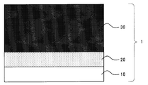
- FIG. 1 is a schematic view showing an example of a layer structure of an optical film according to the present invention.
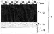
- FIG. 2 is a schematic view showing another example of the layer structure of the optical film according to the present invention.
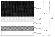
- FIG. 3 is a schematic view showing an example of the layer structure of the polarizing plate according to the present invention.
- the curable resin composition for an antistatic layer according to the present invention (hereinafter sometimes simply referred to as “antistatic layer composition”), an optical film, a polarizing plate and a display panel using the optical film are described. To do.
- (meth) acryloyl represents acryloyl and / or methacryloyl
- (meth) acrylate represents acrylate and / or methacrylate.
- the light of the present invention includes not only visible light and electromagnetic waves having wavelengths in a non-visible region such as ultraviolet rays and X-rays, but also particle beams such as electron beams and radiation or ionizing radiation that collectively refers to electromagnetic waves and particle beams.
- the “hard coat layer” refers to a layer having a hardness of “H” or higher in a pencil hardness test (4.9 N load) specified in JIS K5600-5-4 (1999).
- a sheet is thin and generally refers to a flat product whose thickness is small relative to the length and width.
- a film has a thickness compared to the length and width.
- a thin, flat product that is extremely small and has an arbitrarily limited maximum thickness, usually supplied in the form of a roll. Therefore, it can be said that a film having a particularly thin thickness among the sheets is a film, but the boundary between the sheet and the film is not clear and is difficult to distinguish clearly. Therefore, in the present invention, the meaning of both a thick sheet and a thin sheet is meant. Including “” is defined as “film”.
- the resin is a concept including a polymer in addition to a monomer and an oligomer, and means a component that becomes a matrix of other functional layers such as an antistatic layer and an HC layer after curing.
- the molecular weight means a weight average molecular weight which is a polystyrene equivalent value measured by gel permeation chromatography (GPC) in a THF solvent when having a molecular weight distribution, and when having no molecular weight distribution, It means the molecular weight of the compound itself.
- GPC gel permeation chromatography
- the average particle size of the fine particles means a value measured using a Microtrac particle size analyzer manufactured by Nikkiso Co., Ltd. in the case of fine particles in the composition. It means the average value of 10 particles observed by a transmission electron microscope (TEM) photograph of the cross section of the membrane.
- TEM transmission electron microscope
- osmosis means dissolving or swelling the TAC substrate.
- solid content means the component except a solvent.
- the curable resin composition for an antistatic layer is (A) antistatic agent, (B) a polyfunctional monomer having two or more photocurable groups in one molecule and a molecular weight of 900 or less, and (C) six or more (meth) acryloyl groups in one molecule, and a weight average molecular weight of 1000 to 11,000 urethane acrylates,
- the ratio of (A) to the total amount of (A), (B) and (C) is 1 to 30% by mass
- the ratio of (C) to the total amount of (B) and (C) is 1 to 40% by mass.
- the antistatic layer can be provided with antistatic properties, and this is the case where the HC layer is formed on the antistatic layer having a thickness of 1 to 5 ⁇ m. However, sufficient dust adhesion prevention is ensured. Further, by setting the ratio of urethane acrylate (C) to the total amount of polyfunctional monomer (B) and urethane acrylate (C) within the above range, the antistatic layer and then the HC layer are formed on the TAC substrate from the TAC substrate side.
- the urethane acrylate (C) When formed, the urethane acrylate (C) does not penetrate into the TAC substrate or is harder to penetrate than the polyfunctional monomer (B), so the urethane acrylate (C) is also present at the interface between the antistatic layer and the HC layer.
- the (meth) acryloyl group of the urethane acrylate (C) and the reactive group in the HC layer are cured and bonded, so that sufficient adhesion between the antistatic layer and the HC layer can be obtained.
- the polyfunctional monomer (B) penetrates the TAC substrate moderately (uniformly penetrates with gradation, not the same depth), and the penetrated polyfunctional monomer (B) present in the TAC substrate.
- the reactive group (photo-curable group) of the polyfunctional monomer (B) present in the antistatic layer and the reactive group ((meth) acryloyl group) of the urethane acrylate (C) are cured and bonded. Therefore, adhesion between the antistatic layer and the TAC substrate can also be obtained.
- the components of will be described.
- the antistatic agent (A) imparts conductivity to the antistatic layer or optical film, which is a cured film of the composition for the antistatic layer, to prevent electrification, and dust or dust adheres to it. It is a component that has the property of preventing the occurrence of, i.e., the function of imparting antistatic properties.
- a conventionally known antistatic agent can be used as the antistatic agent (A), and is not particularly limited.
- a cationic compound such as a quaternary ammonium salt described in Patent Document 1, an anionic compound such as a sulfonate group, an amphoteric compound such as an amino acid group, a nonionic compound such as an amino alcohol group, an organometallic compound, and a metal chelate compound
- high molecular weight compounds of these compounds, polymerizable compounds, conductive ultrafine particles such as indium tin oxide (ITO) having an average primary particle size of 1 to 100 nm, and polymer type conductivity such as aliphatic conjugated polyacetylene A composition ITO
- the antistatic agent (A) is a quaternary ammonium salt having a weight average molecular weight of 1,000 to 50,000. It is preferable because it suppresses penetration into the resin and is excellent in coatability. When the above upper limit is exceeded, the coating property of the composition deteriorates, and when below the lower limit, the antistatic agent tends to bleed out at the interface between the antistatic layer and the HC layer, and the antistatic layer and the HC layer Adhesion may be deteriorated.
- the film thickness of the antistatic layer has been provided as a thin film of about 0.1 to 1 ⁇ m in view of optical performance and transparency, but such a thin film layer provides antistatic properties. Since most of the composition in the layer had to be made into an antistatic material, a resin composition having a reactive group necessary for providing adhesion to the base material and the layer on it was sufficient. It was very difficult to add the amount. Therefore, in the present invention, in order to make the film thickness 1-5 ⁇ m thicker than before and to ensure the adhesion between the antistatic layer and the adjacent layer, it has a reactive group other than the antistatic material. The resin composition can be sufficiently added. Since the film thickness increases, it is desirable to select a highly transparent material for the antistatic agent to be added.
- an organic material having higher transparency than the inorganic material is preferable, and among the organic materials, a quaternary ammonium salt with extremely little coloring is optimal.
- a quaternary ammonium salt when used, when the transparent substrate is TAC, it is preferable in that the total light transmittance of the entire optical film can be 90% or more. Further, the haze value can be reduced to 0.5% or less.
- the total light transmittance can be measured according to JIS K7361 (1997), and the haze value can be measured with HM150 manufactured by Murakami Color Research Laboratory according to JIS K7136 (2000).
- the quaternary ammonium salt has a photocurable group from the viewpoint of improving the adhesion between the antistatic layer and the HC layer by a crosslinking reaction with the binder component of the HC layer.
- the photocurable group is preferably a polymerizable unsaturated group, and more preferably an ionizing radiation curable unsaturated group. Specific examples thereof include a group having an ethylenically unsaturated bond such as a (meth) acryloyl group, a (meth) acryloyloxy group, a vinyl group and an allyl group, and an epoxy group.
- Examples of commercially available quaternary ammonium salts having a weight average molecular weight of 1,000 to 50,000 include, for example, trade name H6100 manufactured by Mitsubishi Chemical Corporation and trade name Uniresin AS-10 manufactured by Shin-Nakamura Chemical Co., Ltd. / M, Uniresin AS-12 / M, Uniresin AS-15 / M, and Uniresin ASH26.
- the antistatic agent (A) is contained in an amount of 1 to 30% by mass based on the total amount of the antistatic agent (A), the polyfunctional monomer (B) and the urethane acrylate (C) described later. ing. If the proportion of the antistatic agent (A) is less than 1% by mass relative to the total amount (A + B + C), sufficient antistatic performance cannot be obtained. Moreover, when the proportion of the antistatic agent (A) exceeds 30% by mass with respect to the total amount (A + B + C), the proportion of the polyfunctional monomer (B) and the urethane acrylate (C) in the antistatic layer composition is decreased.
- the proportion of the antistatic agent (A) is 1 to 30% by mass, preferably 5 to 20% by mass, based on the total amount (A + B + C).
- the polyfunctional monomer (B) is one of binder components that are cured to form a matrix of the antistatic layer, and is a monomer having a molecular weight of 900 or less having two or more photocurable groups in one molecule. It is a component that contributes to improving adhesion by increasing the crosslink density with the HC layer in the antistatic layer or adjacent to the antistatic layer by having a low molecular weight and polyfunctionality. Further, at least a part of the polyfunctional monomer penetrates into the TAC base material and is cured, thereby contributing to improvement in adhesion between the antistatic layer and the TAC base material.
- the molecular weight of the polyfunctional monomer (B) exceeds 900, the permeability to the TAC substrate is lowered, and sufficient adhesion between the antistatic layer and the TAC substrate may not be obtained.
- the molecular weight of the polyfunctional monomer (B) may be 900 or less, but the penetration of the polyfunctional monomer (B) into the TAC base material is moderated, and the adhesion between the antistatic layer and the HC layer and the antistatic property From the viewpoint of highly satisfying (surface resistance value), the molecular weight of the polyfunctional monomer (B) is preferably 230 or more, and more preferably 290 or more.
- the polyfunctional monomer (B) may not penetrate into the TAC base material properly, and may penetrate into a uniform depth and generate a new interface. There is a possibility that optical interference occurs between the light reflected at, the light reflected at the interface between the antistatic layer and the HC layer, and the light reflected from the surface of the HC layer, resulting in interference fringes and deterioration of the appearance.
- the number of photocurable groups of the polyfunctional monomer (B) is 2 or more in order to form a crosslinked structure, but preferably 3 or more, more preferably 5 or more. If the number is 3 or more, sufficient adhesion between the antistatic layer, the HC layer, and the TAC substrate is easily obtained.
- Examples of the photocurable group include the same ones as mentioned for the antistatic agent.
- Examples of the polyfunctional monomer (B) include pentaerythritol tri (meth) acrylate, dipentaerythritol hexa (meth) acrylate, dipentaerythritol penta (meth) acrylate, trimethylolpropane tri (meth) acrylate, and trimethylolpropane hexa. Examples thereof include (meth) acrylates and modified products thereof. Examples of modified products include EO (ethylene oxide) modified products, PO (propylene oxide) modified products, CL (caprolactone) modified products, and isocyanuric acid modified products.
- the photocurable group is preferably an acryloyl group rather than a methacryloyl group.
- the polyfunctional monomer (B) dipentaerythritol pentaacrylate (DPPA) and dipentaerythritol hexaacrylate (DPHA) are particularly preferably used.
- the polyfunctional monomer (B) satisfies the above-mentioned content ratio of the antistatic agent, and the total amount of the polyfunctional monomer (B) and urethane acrylate (C) described later.
- the content is 60 to 99% by mass. If it is less than 60% by mass, sufficient adhesion between the antistatic layer, the HC layer and the TAC substrate cannot be obtained. Moreover, when it exceeds 99 mass%, the ratio of urethane acrylate (C) is small, and sufficient adhesion between the antistatic layer and the HC layer cannot be obtained.
- Urethane acrylate (C) is one of the binder components that harden to become the matrix of the antistatic layer, has 6 or more (meth) acryloyl groups in one molecule, and has a weight average molecular weight of 1000 to 11000. , Preferably 1000 to 10000, more preferably 1000 to 5000. When the weight average molecular weight is 1000 to 11000, the coating property is good, it does not penetrate into the TAC base material or is harder to penetrate than the polyfunctional monomer (B), the penetration is easy to control, and the antistatic layer is surely Present throughout.
- the antistatic agent (A) is a quaternary ammonium salt
- the binder in the antistatic layer is a compound having an OH group
- the antistatic agent is excessively dispersed throughout the layer, thus preventing the antistatic. Sex cannot be obtained.
- DPHA does not contain an OH group in terms of structural formula, it is generally difficult to make it 100% hexafunctional in the synthesis, so it is known that it is actually a mixed compound with pentafunctional or tetrafunctional moieties.
- a commercially available resin is a compound in which an OH group remains, so that a preferable antistatic property cannot be obtained.
- urethane acrylate (C) that is a hydrophobic resin that can control the dispersibility.
- the antistatic agent (A) is a quaternary ammonium salt system
- the antistatic agent is excessively dispersed in the layer, or Bleed out in the interface direction can be reliably controlled.
- the quaternary ammonium salt prefers hydrophilicity because it tends to bleed out in the HC interface direction. Therefore, when the antistatic layer is laminated and cured, air is present on its surface, and moisture in the air is present. It is because it bleeds out in response to.
- the crosslink density with the reactive groups in the antistatic layer or in the HC layer adjacent to the antistatic layer is increased, and the adhesion between the antistatic layer and the HC layer is improved.
- the reactive group of the polyfunctional monomer (B) of the antistatic layer penetrating into the TAC substrate is a reactive group of the (meth) acryloyl group of the urethane acrylate (C) or the polyfunctional monomer present in the antistatic layer. Therefore, the urethane acrylate (C) contributes to the improvement of the adhesion between the antistatic layer and the TAC substrate.
- the urethane acrylate (C) is not added, and any polyfunctional monomer (B) having many reactive groups other than the antistatic agent (A) may be used.
- any polyfunctional monomer (B) having many reactive groups other than the antistatic agent (A) may be used.
- the polyfunctional monomer (B) alone in order to control the movement of the antistatic agent (A) in the antistatic layer, it is difficult to control with the polyfunctional monomer (B) alone, and since the antistatic agent (A) is not dispersed, it is hydrophobic.
- urethane acrylate (C) having many reactive groups is essential.
- containing urethane acrylate (C) is also effective in suppressing curling (warping).
- the weight average molecular weight of the urethane acrylate (C) is less than 1000, the urethane acrylate (C) easily penetrates into the TAC substrate, and penetrates too much into the TAC substrate, and acryloyl groups at the interface between the antistatic layer and the HC layer are formed. There is a risk that the adhesion between the antistatic layer and the HC layer may be difficult to obtain. If the weight average molecular weight of the urethane acrylate (C) exceeds 11,000, the coatability may be deteriorated.
- the urethane acrylate (C) has 6 or more (meth) acryloyl groups, it may contain other crosslinking reactive functional groups such as ionizing radiation-curable unsaturated groups.
- the (meth) acryloyl group may be 6 or more in total including the acryloyl group and methacryloyl group, may have only acryloyl group, or may have only methacryloyl group.
- the urethane acrylate (C) of the present invention is not particularly limited as long as it has a urethane bond (—NH—CO—O—), has 6 or more (meth) acryloyl groups, and has the above weight average molecular weight. .
- the urethane acrylate (C) is preferably a translucent material that transmits light when formed into a coating film, an ionizing radiation curable urethane acrylate that is a resin that is cured by ionizing radiation represented by ultraviolet rays or electron beams, and other publicly known ones.
- the urethane acrylate or the like may be appropriately employed depending on the required performance.
- urethane acrylate Commercially available products of the urethane acrylate include, for example, trade name UV1700B manufactured by Nippon Synthetic Chemical Industry Co., Ltd. described in Patent Document 1, trade name UN3320HS manufactured by Negami Kogyo Co., Ltd., trade name manufactured by Arakawa Chemical Industries, Ltd. Examples include BS577 and trade names U15HA, U15H, U9HA, U9H, U6HA and U6H manufactured by Shin-Nakamura Chemical Co., Ltd.
- the urethane acrylate (C) satisfies the above-described content ratio of the antistatic agent and is 1 with respect to the total amount of the polyfunctional monomer (B) and the urethane acrylate (C). ⁇ 40% by weight. If it is less than 1% by mass, sufficient adhesion between the antistatic layer and the HC layer cannot be obtained. Moreover, when it exceeds 40 mass%, the ratio of a polyfunctional monomer (B) will be small, and sufficient adhesiveness of an antistatic layer and a TAC base material will not be obtained.
- the proportion of the urethane acrylate (C) is 1 to 40% by mass, preferably 5 to 30% by mass, based on the total amount (B + C).
- the antistatic agent (A) may be excessively dispersed in the antistatic layer. In this way, the layers can be present at a level where antistatic properties can be exhibited. With this composition, the surface low efficiency of the antistatic layer can be less than 1 ⁇ 10 12 ⁇ / ⁇ .
- the antistatic layer composition may contain a solvent and a polymerization initiator as necessary.
- these other components will be described.
- solvent examples include ketone solvents such as acetone described in Patent Document 1, ester solvents such as methyl acetate, nitrogen-containing solvents such as acetonitrile, glycol solvents such as methyl glycol, ether solvents such as THF, and methylene chloride.
- a permeable solvent such as a halogenated hydrocarbon solvent such as methyl glycol solvent and a methyl ether solvent such as methyl cellosolve can be used.
- the penetrating solvent is preferably at least one selected from the group consisting of methyl acetate, ethyl acetate, butyl acetate, methyl ethyl ketone, methyl isobutyl ketone (MIBK) and cyclohexanone.
- non-permeable solvents such as propylene glycol monomethyl ether (PGME), normal propanol, isopropanol, normal butanol, sec-butanol, isobutanol and tert-butanol may be used.
- PGME propylene glycol monomethyl ether
- the said solvent may be used individually by 1 type, and may mix and use 2 or more types.
- a permeable solvent by using a permeable solvent, the penetration of the polyfunctional monomer (B) into the TAC substrate is promoted, and the adhesion between the antistatic layer and the TAC substrate is improved. Then, since it is estimated, it is preferable to use a permeable solvent.
- the antistatic layer composition of the present invention by using a non-permeable solvent, the penetration of the urethane acrylate (C) into the TAC substrate is suppressed, and the adhesion between the antistatic layer and the HC layer is improved. Since it is estimated that it improves, it is preferable to use a non-permeable solvent.
- a penetrating solvent when there is only one solvent, but in the case of two or more kinds of solvents, a combination of a penetrating solvent and a non-permeable solvent is used. Most preferably, it is used. Even one type (only penetrating solvent) can control penetration by the molecular weight of urethane acrylate (C), but the combination of penetrating solvent and non-penetrating solvent makes it easier to control penetrating and uses composition. This is because the stable performance of the antistatic layer can be obtained.
- the amount is preferably 30 to 500 parts by mass with respect to 100 parts by mass of the total solid content of the composition.
- a polymerization initiator is a component which starts or accelerates
- the radical polymerization initiator for example, trade name Irgacure 184 (1-hydroxy-cyclohexyl-phenyl-ketone) manufactured by Ciba Japan Co., Ltd. is preferably used.
- a polymerization initiator When a polymerization initiator is used, its content is preferably 0.4 to 2.0% by mass with respect to the total mass of the total solid content of the antistatic layer composition.
- the curable resin composition for an antistatic layer can be obtained by mixing and dispersing the components (A), (B), and (C) in a solvent. Further, when the component (A), (B) or (C) has sufficient fluidity even without a solvent, the solvent may be omitted.
- a known method such as a paint shaker or a bead mill can be used for mixing and dispersing.
- the cured product having a film thickness of 1 to 5 ⁇ m of the curable resin composition for an antistatic layer. It is also possible to make the surface resistance value of less than 1 ⁇ 10 12 ⁇ / ⁇ . Since the antistatic layer has such an antistatic performance, even if a relatively thick HC layer is laminated, it is possible to exhibit an excellent dust adhesion preventing performance in the entire optical film.
- the film thickness of the antistatic layer is less than 1 ⁇ m, it is necessary to increase the amount of the quaternary ammonium salt as an antistatic agent in order to maintain the same surface resistance. There is a possibility that the number of groups decreases and the adhesion between the antistatic layer and the HC layer deteriorates. When the film thickness of the antistatic layer exceeds 5 ⁇ m, surface resistance tends to be manifested, but curling occurs, costs increase, and handling properties may deteriorate.
- the antistatic agent (A) is 5 to 20% by mass based on the total amount of the antistatic agent (A), the polyfunctional monomer (B) and the urethane acrylate (C), and urethane.
- the acrylate (C) 5 to 30% by mass based on the total amount of the polyfunctional monomer (B) and the urethane acrylate (C)
- UV (UV) for adhesiveness of the optical film Excellent durability is also obtained.
- the optical film according to the present invention is an optical film in which an antistatic layer having a thickness of 1 to 5 ⁇ m and a hard coat layer are provided adjacent to one side of a triacetylcellulose substrate from the side of the triacetylcellulose substrate.
- the antistatic layer is made of a cured product of the curable resin composition for the antistatic layer, and the polyfunctional monomer (B) is present in the region on the interface side of the antistatic layer side of the triacetyl cellulose substrate. Is characterized in that it penetrates and hardens.
- the antistatic layer is the curable resin for the antistatic layer.
- the adhesion between the HC layer and the antistatic layer is excellent while having sufficient dust adhesion prevention properties.
- the adhesion between the antistatic layer and the TAC substrate can also be obtained by the penetration of the polyfunctional monomer (B) into the region on the interface side of the TAC substrate on the antistatic layer side. As an entire optical film, excellent dust adhesion prevention performance can be obtained.
- the antistatic layer is formed from a cured product of the antistatic layer composition, whereby the hard coat layer, the antistatic layer, and the triacetyl of the optical film are formed.
- the adhesion rate may be 80 to 100%.
- This adhesion rate represents adhesion between the HC layer, the antistatic layer and the TAC substrate, that is, adhesion between the antistatic layer and the HC layer and adhesion between the antistatic layer and the TAC substrate.
- the antistatic layer By forming the antistatic layer by curing the above antistatic layer composition, it has excellent adhesion between the antistatic layer having a film thickness of 1 to 5 ⁇ m and the HC layer, and adhesion between the antistatic layer and the TAC substrate. Excellent adhesion as a whole. In particular, this adhesion is remarkable after the UV resistance test.
- the optical film according to the present invention exhibits excellent adhesion even after the UV resistance test.
- FIG. 1 is a schematic view showing an example of a layer structure of an optical film according to the present invention.
- An antistatic layer 20 and a hard coat layer 30 are provided adjacent to each other in this order on one side of the triacetyl cellulose substrate 10.
- FIG. 2 is a schematic view showing another example of the layer structure of the optical film according to the present invention.
- a low refractive index layer 40 is further provided on the hard coat layer of the same optical film as in FIG.
- a triacetyl cellulose base material, an antistatic layer and a hard coat layer, which are essential components of the optical film according to the present invention and a high refractive index layer, a medium refractive index layer, a low refractive index layer which can be appropriately provided as necessary.
- Other layers such as a refractive index layer, an antiglare layer, and an antifouling layer will be described.
- the triacetyl cellulose base material used in the present invention is a triacetyl cellulose film having a high light transmittance, and is not particularly limited as long as it satisfies physical properties that can be used as a light transparent base material of an optical film.
- a conventionally known TAC substrate of a hard coat film or an optical film can be appropriately selected and used.
- the average light transmittance of the TAC substrate in the visible light region of 380 to 780 nm is preferably 80% or more, particularly preferably 90% or more.
- the light transmittance is measured using a value measured in the air at room temperature using an ultraviolet-visible spectrophotometer (for example, trade name UV-3100PC manufactured by Shimadzu Corporation).
- a surface treatment such as saponification treatment or provision of a primer layer may be applied to the TAC substrate.
- additives such as an antistatic agent may be added.
- the thickness of the TAC substrate is not particularly limited, and is usually 30 to 200 ⁇ m, preferably 40 to 200 ⁇ m.
- the antistatic layer of the present invention comprises a cured product of the curable resin composition for an antistatic layer and has a thickness of 1 to 5 ⁇ m. If the film thickness is less than 1 ⁇ m, sufficient antistatic performance cannot be obtained, and an essential binder cannot be sufficiently added to ensure adhesion with other layers. If it is thicker than 5 ⁇ m, the antistatic agent cannot exert its performance unless it exists in the layer to some extent, so that the curability of the antistatic layer is increased, the workability is deteriorated, and the film thickness is further increased. The amount of antistatic agent and the like increases, resulting in an increase in cost.
- the surface resistance is preferably less than 1 ⁇ 10 12 ⁇ / ⁇ , more preferably 1 ⁇ 10 11 ⁇ / ⁇ or less, and further preferably 1 ⁇ 10 10 ⁇ / ⁇ or less. If the surface resistance of the antistatic layer is good, the dust adhesion preventing property of the optical film laminated with the HC layer may be further improved.
- the hard coat layer is a layer showing a hardness of “H” or higher in the pencil hardness test (4.9 N load) specified in JIS K5600-5-4 (1999), and the optical film according to the present invention has a hardness.
- the HC layer is composed of a cured product of the composition for hard coat layer, may be a conventionally known hard coat layer, or may be composed of a cured product of the composition for hard coat layer containing only the binder component.
- the polymerization initiators and the like mentioned in the antistatic layer composition may be contained in the composition.
- a reactive silica fine particle having a crosslinking reactivity with a component imparting conventionally known hardness for example, a binder component described in JP-A-2008-165040 may be contained. .
- a resin composition containing an ionizing radiation curable resin as a transparent resin is applied to a transparent substrate, and monomers, oligomers and prepolymers contained in the resin composition are crosslinked and / or polymerized.
- an HC layer can be formed.
- an ionizing radiation curable resin is preferable, and as a functional group of the monomer, oligomer and prepolymer, an ionizing radiation polymerizable functional group is preferable, and a photopolymerizable functional group is particularly preferable. Sufficient adhesion between the antistatic layer and the HC layer can be obtained by this functional group being cured and bonded to the reactive group of the urethane acrylate (C) in the resin composition for the antistatic layer.
- Examples of the photopolymerizable functional group include unsaturated polymerizable functional groups such as a (meth) acryloyl group, a vinyl group, a styryl group, and an allyl group.
- Examples of the prepolymer and oligomer include acrylates such as urethane (meth) acrylate, polyester (meth) acrylate, and epoxy (meth) acrylate, unsaturated polyester, and epoxy resin.
- Monomers include styrene monomers such as styrene and ⁇ -methylstyrene; methyl (meth) acrylate, 2-ethylhexyl (meth) acrylate, pentaerythritol (meth) acrylate, pentaerythritol tri (meth) acrylate, pentaerythritol Tetra (meth) acrylate, pentaerythritol ethoxytetra (meth) acrylate, dipentaerythritol hexa (meth) acrylate, dipentaerythritol penta (meth) acrylate, trimethylolpropane tri (meth) acrylate, trimethylolpropane ethoxytri (meth) Acrylate, glycerin propoxytriacrylate, ditrimethylolpropane tetraacrylate, polyethylene glycol di (meth) acrylate, bis Eno
- it is preferably a polyfunctional acrylate monomer, and among them, pentaerythritol tri (meth) acrylate, pentaerythritol tetra (meth) acrylate, dipentaerythritol hexa (meth).
- Acrylate and dipentaerythritol penta (meth) acrylate are more preferred because they have good adhesion to the antistatic layer and good pencil hardness.
- an oligomer component such as urethane polyfunctional acrylate with these monomers because the hardness can be improved, polymerization shrinkage can be reduced, and curling and crack prevention can be improved.
- inorganic fine particles such as silica may be contained for improving the hardness.
- the organic surface treatment may be performed and you may have a reactive group.
- a polymer to the resin composition as a binder.
- the polymer include polymethyl methacrylate (PMMA) and cellulose acetate propionate (CAP).
- PMMA polymethyl methacrylate
- CAP cellulose acetate propionate
- a radical photopolymerization initiator can be added to the resin composition as necessary.
- a preferable addition amount is 0.8 to 8.0% by mass with respect to the total mass of the total solid content of the resin composition.
- the radical photopolymerization initiator acetophenones, benzoins, benzophenones, phosphine oxides, ketals, anthraquinones, thioxanthones, azo compounds and the like are used.
- acetophenones 2,2-dimethoxyacetophenone, 2,2-diethoxyacetophenone, p-dimethylacetophenone, 1-hydroxy-dimethylphenylketone, 1-hydroxy-dimethyl-p-isopropylphenylketone, 1-hydroxycyclohexylphenyl Ketone, 2-methyl-4-methylthio-2-morpholinopropiophenone, 2-benzyl-2-dimethylamino-1- (4-morpholinophenyl) -butanone, 4-phenoxydichloroacetophenone, 4-t-butyl-
- benzoins include benzoin, benzoin methyl ether, benzoin ethyl ether, benzoin isopropyl ether, benzyl dimethyl ketal, and benzoin benzene sulfonic acid. Ester, benzoin toluenesulfonic acid ester, benzoin methyl ether, benzoin ethyl ether
- Benzophenones include benzophenone, hydroxybenzophenone, 4benzoyl-4′-methyldiphenyl sulfide, 2,4-dichlorobenzophenone, 4,4-dichlorobenzophenone and p-chlorobenzophenone, 4,4′-dimethylaminobenzophenone ( Michler's ketone), 3,3 ′, 4,4′-tetra (t-butylperoxycarbonyl) benzophenone and the like can be used.
- a photosensitizer can be mixed and used, and specific examples thereof include n-butylamine, triethylamine, poly-n-butylphosphine and the like.
- the film thickness of the HC layer may be adjusted as appropriate, for example, 1 to 20 ⁇ m. Preferably, it is 5 to 15 ⁇ m. If it exceeds 15 ⁇ m, excellent dust adhesion preventing performance cannot be obtained, and if it is less than 5 ⁇ m, the hardness becomes insufficient and the adhesion also becomes weak. Normally, when the HC layer laminated on the antistatic layer becomes thick, the dust adhesion preventing performance deteriorates. However, with the configuration and composition of the present application, excellent dust adhesion preventing performance can be obtained.
- the optical film according to the present invention even if a thick HC layer is laminated on the antistatic layer such that the antistatic layer is 1 to 5 ⁇ m and the HC layer is 5 to 15 ⁇ m.
- the optical film can provide sufficient dust adhesion prevention performance and sufficient adhesion between the antistatic layer and the HC layer.
- the antireflection, antiglare and antifouling properties of the optical film are provided on the surface of the HC layer opposite to the antistatic layer without departing from the spirit of the present invention.
- other layers such as a high refractive index layer, a medium refractive index layer, a low refractive index layer, an antiglare layer, and an antifouling layer may be provided.
- the high refractive index layer and the medium refractive index layer are layers provided for adjusting the reflectance of the optical film according to the present invention.
- a high refractive index layer although not shown, it is usually provided adjacent to the TAC substrate side of the low refractive index layer.
- a middle refractive index layer although not shown, it is usually provided in the order of a middle refractive index layer, a high refractive index layer, and a low refractive index layer from the TAC substrate side.
- the high refractive index layer and the middle refractive index layer are made of a cured product of a composition mainly containing a binder component and refractive index adjusting particles.
- a binder component the polyfunctional monomer etc. which were mentioned by the composition for antistatic layers can be used.
- the particles for adjusting the refractive index include fine particles having a particle size of 100 nm or less. Examples of such fine particles include zinc oxide (refractive index: 1.90), titania (refractive index: 2.3 to 2.7), ceria (refractive index: 1.95), and tin-doped indium oxide (refractive index: 1). .95), at least one selected from the group consisting of antimony-doped tin oxide (refractive index: 1.80), yttria (refractive index: 1.87), and zirconia (refractive index: 2.0). it can.
- the high refractive index layer preferably has a refractive index of 1.50 to 2.80.
- the medium refractive index layer has a low refractive index for the high refractive index layer, and preferably has a refractive index of 1.50 to 2.00.
- the film thicknesses of the high refractive index layer and the medium refractive index layer may be appropriately adjusted, and are preferably 50 to 300 nm.
- the low refractive index layer is a cured product of a composition containing a low refractive index component such as silica or magnesium fluoride and a binder component or a composition for a low refractive index layer containing a fluorine-containing resin such as a vinylidene fluoride copolymer.
- a conventionally known low refractive index layer can be obtained.
- the composition for forming the low refractive index layer may contain hollow particles in order to reduce the refractive index of the low refractive index layer.
- a hollow particle refers to a particle having an outer shell layer and the inside surrounded by the outer shell layer being a porous structure or a cavity.
- the porous structure or cavity contains air (refractive index: 1), and the refractive index of the low refractive index layer is obtained by incorporating hollow particles having a refractive index of 1.20 to 1.45 in the low refractive index layer. Can be reduced.
- the average particle diameter of the hollow particles is preferably 1 to 100 nm.
- the hollow particles those conventionally used for a low refractive index layer can be used, and examples thereof include fine particles having voids described in JP-A-2008-165040.
- the number average primary particle size of the fatty acid metal salt particles is less than the lower limit, problems such as aggregation of the fatty acid metal salt particles and embedding of the fatty acid metal salt particles in the colored resin particles are likely to occur. May adversely affect printing performance.
- the toner particles may not be sufficiently imparted with a function of imparting charging stability, fluidity, etc. to the toner particles, which may adversely affect toner printing performance.
- the antiglare layer is composed of a cured product of a composition for an antiglare layer containing a binder component and an antiglare agent, and the multifunctional monomer described in the above composition for an antistatic layer can be used as the binder component.
- the antiglare agent include fine particles, and examples thereof include styrene beads (refractive index 1.59), melamine beads (refractive index 1.57), and acrylic beads (refractive index 1.49).
- the average particle size of such fine particles imparting antiglare properties is preferably 100 to 500 nm.
- the content of the fine particles imparting the antiglare property is preferably 2 to 30% by mass with respect to the total mass of the binder component contained in the composition for the antiglare layer.
- an antifouling layer can be provided on the outermost surface of the optical film opposite to the TAC substrate for the purpose of preventing the outermost surface of the optical film from being stained.
- the antifouling layer makes it possible to further improve the antifouling property and scratch resistance of the optical film.
- the antifouling layer comprises a cured product of the antifouling layer composition containing an antifouling agent and a binder component.
- a conventionally well-known thing may be used for the binder component of the composition for antifouling layers, for example, the polyfunctional monomer quoted by the said composition for antistatic layers can be used.
- the antifouling agent contained in the antifouling layer composition can be appropriately selected from antifouling agents such as known leveling agents, and one or more can be used.
- the content of the antifouling agent is preferably 0.1 to 5% by mass with respect to the total mass of the binder component contained in the antifouling layer composition.
- the method for producing the optical film of the present invention is not particularly limited as long as it is a method capable of obtaining the layer configuration of the optical film described above, and a conventionally known method can be used.
- a step of preparing a triacetyl cellulose base material (ii) a step of preparing the composition for antistatic layer and the composition for hard coat layer, (iii) one side of the TAC base material (Iv) a step of applying the antistatic layer composition to form a coating film, (iv) irradiating the coating film of the antistatic layer composition with light and curing to form an antistatic layer, (v) A step of applying the hard coat layer composition on the antistatic layer to form a coating film, (vi) a step of irradiating the coating film of the composition for HC layer with light and curing to form an HC layer.
- composition of the composition for an antistatic layer is not completely cured (full cure) in the step (iv), but is semi-cured (half cured), and the composition for the HC layer is formed on the half-cured coating.
- An optical film may be obtained by applying a product to form a coating film, irradiating the half-cured coating film and the coating film of the HC layer composition together with light irradiation, and performing full curing.
- the coating method may be a conventionally known method, and is not particularly limited. Gravure coating method, spin coating method, dipping method, spray method, slide coating method, bar coating method, roll coater method, meniscus coater method, flexographic printing Various methods such as a method, a screen printing method, and a pea coater method can be used.
- ultraviolet rays For light irradiation, ultraviolet rays, visible light, electron beams, ionizing radiation, or the like is mainly used.
- ultraviolet curing ultraviolet rays or the like emitted from light such as an ultrahigh pressure mercury lamp, a high pressure mercury lamp, a low pressure mercury lamp, a carbon arc, a xenon arc, or a metal halide lamp are used.
- the irradiation amount of the energy ray source is 50 to 500 mJ / cm 2 as an integrated exposure amount at an ultraviolet wavelength of 365 nm.
- the irradiation dose is 5 to 50 mJ / cm 2 .
- the treatment is usually performed at a temperature of 40 ° C to 120 ° C.
- the drying method After applying the antistatic layer composition, it may be dried before light irradiation.
- the drying method include reduced-pressure drying or heat drying, and a method combining these drying methods.
- drying at normal pressure drying at 30 to 110 ° C. is preferable.
- the temperature is in the range of room temperature to 80 ° C., preferably 40 ° C. to 70 ° C., and is 20 seconds to 3 minutes, preferably 30 seconds to 1 minute.
- the drying process can be performed in time.
- compositions such as the HC layer and the low refractive index layer may be prepared by the same method as the antistatic layer.
- the above antistatic layer coating method or curing method can be used.
- FIG. 3 is a schematic diagram showing an example of the layer structure of the polarizing plate according to the present invention.
- the polarizing plate 80 shown in FIG. 3 has the optical film 1 and the polarizer 70 in which the protective film 50 and the polarizing layer 60 are laminated, and the polarizer 70 is disposed on the triacetylcellulose substrate 10 side of the optical film 1. Is provided.
- the polarizer is disposed on the triacetyl cellulose base material side of the optical film, not only when the optical film and the polarizer are separately formed, but also the members constituting the optical film constitute the polarizer. It also includes the case of serving also as a member.
- the display panel is usually disposed on the polarizer side.
- the polarizer used in the present invention is not particularly limited as long as it has predetermined polarization characteristics, and a polarizer generally used in a liquid crystal display device can be used.
- the form of the polarizer is not particularly limited as long as the predetermined polarization characteristics can be maintained for a long period of time.
- the polarizer may be composed of only the polarizing layer, and the protective film and the polarizing layer are bonded together. It may be a thing. When the protective film and the polarizing layer are bonded together, the protective film may be formed only on one side of the polarizing layer, or the protective film may be formed on both sides of the polarizing layer.
- polarizing layer usually, a film made of polyvinyl alcohol is impregnated with iodine, and this is uniaxially stretched to form a complex of polyvinyl alcohol and iodine.
- the protective film is not particularly limited as long as it can protect the polarizing layer and has a desired light transmittance.
- the light transmittance of the protective film the transmittance in the visible light region is preferably 80% or more, and more preferably 90% or more.
- the transmittance of the protective film can be measured according to JIS K7361-1 (plastic-transparent material total light transmittance test method).
- the resin constituting the protective film examples include cellulose derivatives, cycloolefin resins, polymethyl methacrylate, polyvinyl alcohol, polyimide, polyarylate, and polyethylene terephthalate. Among them, it is preferable to use a cellulose derivative or a cycloolefin resin.
- the protective film may be a single layer or may be a laminate of a plurality of layers.
- the protective film is a laminate of a plurality of layers, a plurality of layers having the same composition may be laminated, or a plurality of layers having different compositions may be laminated.
- the thickness of the protective film can make the flexibility of the polarizing plate of the present invention within a desired range, and by bonding to the polarizing layer, the dimensional change of the polarizer can be within a predetermined range.
- it is not particularly limited as long as it is within the range, it is preferably within a range of 5 to 200 ⁇ m, particularly preferably within a range of 15 to 150 ⁇ m, and more preferably within a range of 30 to 100 ⁇ m. preferable.
- the thickness is less than 5 ⁇ m, the dimensional change of the polarizing plate of the present invention may increase.
- the said thickness is thicker than 200 micrometers, when cutting the polarizing plate of this invention, there exists a possibility that a process waste may increase or abrasion of a cutting blade may become quick.
- the protective film may have a phase difference.
- the protective film has a phase difference is not particularly limited as long as a desired retardation can be exhibited.
- the protective film has a configuration consisting of a single layer, and includes an optical property developing agent that expresses retardation, and has retardation, and the above-described resin.
- an embodiment having retardation can be mentioned. In the present invention, any of these embodiments can be suitably used.
- the display panel according to the present invention is characterized in that a display is disposed on the triacetylcellulose substrate side of the optical film.
- Examples of the display include LCD, PDP, ELD (organic EL, inorganic EL), CRT, touch panel, electronic paper, and tablet PC.
- the display panel according to the present invention can also be used for touch panels, electronic paper, tablet PCs, and the like.
- the LCD which is a typical example of the display, is a transmissive type, and includes a transmissive display body and a light source device that irradiates it from the back.
- the display is an LCD
- the optical film of the present invention and the polarizing plate including the optical film are arranged on the surface of the transmissive display body.
- a PDP which is another example of the display, includes a front glass substrate and a rear glass substrate disposed so as to be opposed to the front glass substrate with a discharge gas sealed therebetween.
- the optical film is also provided on the surface of the surface glass substrate or the front plate (glass substrate or film substrate).
- a light emitter such as zinc sulfide or a diamine substance that emits light when a voltage is applied is vapor-deposited on a glass substrate, and an ELD device that performs display by controlling the voltage applied to the substrate or an electric signal is converted into light. It may be a display such as a CRT that generates a visible image. In this case, the optical film is provided on the outermost surface of the ELD device or CRT or the surface of the front plate.
- Antistatic layer composition 1 An antistatic layer composition 1 and an HC layer composition 1 having the following compositions were prepared.
- Antistatic layer composition 1 Antistatic agent (A): Nippon Kasei Co., Ltd. product name UV-ASHC-01 (weight average molecular weight 20000, solid content 70%, quaternary ammonium salt component is 15% in solid content): 1 mass in terms of solid content
- Parts polyfunctional monomer B): dipentaerythritol hexaacrylate (DPHA) (trade name: KAYARAD DPHA, manufactured by Nippon Kayaku Co., Ltd., 6 functional, molecular weight 578): 64 parts by mass Urethane acrylate (C): Arakawa Chemical Industries Trade name BS577 (6-functional, weight average molecular weight 1000) manufactured by Co., Ltd .: 35 parts by mass Polymerization initiator: Trade name Irgacure 184 (1-hydroxycyclohexyl phenyl ketone) manufactured by Ciba Specialty Chemical
- composition 1 for HC layer Dipentaerythritol hexaacrylate (trade name: KAYARAD DPHA, Nippon Kayaku Co., Ltd., 6 functional, molecular weight 578): 98 parts by mass Polymerization initiator: Trade name Irgacure 184 (1) manufactured by Ciba Specialty Chemicals Co., Ltd. -Hydroxycyclohexyl phenyl ketone): 4 parts by mass Methyl ethyl ketone: 100 parts by mass
- Example 1 A TAC substrate having a thickness of 80 ⁇ m (trade name TF80UL manufactured by Fuji Film Co., Ltd.) was prepared, and the prepared composition 1 for antistatic layer was applied to one side of the TAC substrate, and a heating oven at a temperature of 70 ° C. In the film for 60 seconds, the solvent in the coating film is evaporated, and the coating film is cured by irradiating ultraviolet rays so that the integrated light quantity is 50 mJ. Formed.
- TF80UL manufactured by Fuji Film Co., Ltd.
- the hard coat layer composition 1 prepared above is applied onto the obtained antistatic layer, dried in the same manner as the antistatic layer, and the coating film is cured by irradiating ultraviolet rays so that the integrated light quantity becomes 150 mJ. Then, a hard coat layer having a thickness of 12 ⁇ m at the time of drying was formed, and thereby an optical film having an antistatic layer and a hard coat layer in order from the TAC substrate side on one side of the TAC substrate was produced.
- the antistatic layer is formed on the TAC substrate (TF80UL) in the same manner as the optical film, and only the antistatic layer is provided on one side of the TAC substrate.
- the laminated body which has was also produced.
- Example 2 Example 7
- the amounts or types of the antistatic agent (A), polyfunctional monomer (B) and urethane acrylate (C) contained in the antistatic layer composition 1 were changed as shown in Table 1, respectively. Except for the above, an optical film and a laminate were produced in the same manner as in Example 1.
- the urethane acrylate (C) used in Example 7 is trade name UV-7610B (manufactured by Nippon Gosei).
- Example 2 Comparative Examples 1 and 2
- the amounts of the antistatic agent (A), polyfunctional monomer (B) and urethane acrylate (C) contained in the antistatic layer composition 1 were changed as shown in Table 1, respectively.
- An optical film and a laminate were produced in the same manner as in Example 1.
- Example 3 (Comparative Example 3)
- R128H monofunctional, molecular weight 222) manufactured by Nippon Kayaku Co., Ltd. was used instead of DPHA for the polyfunctional monomer (B) contained in the composition 1 for antistatic layer, and an antistatic agent (
- An optical film and a laminate were produced in the same manner as in Example 1 except that the amounts of A), polyfunctional monomer (B) and urethane acrylate (C) were changed as shown in Table 1, respectively.
- Example 4 In Example 1, the polyfunctional monomer (B) contained in the antistatic layer composition 1 was replaced with DPHA using DPCA60 (hexafunctional, molecular weight 1263) manufactured by Nippon Kayaku Co., Ltd. An optical film and a laminate were produced in the same manner as in Example 1 except that the amounts of A), the polyfunctional monomer (B), and the urethane acrylate (C) were changed as shown in Table 1, respectively.
- Example 5 (Comparative Example 5)
- the urethane acrylate (C) contained in the antistatic layer composition 1 was replaced with BS577 by using EBECRYL270 (bifunctional, molecular weight 1500) manufactured by Daicel Cytec Co., Ltd. ),
- An optical film and a laminate were produced in the same manner as in Example 1 except that the amounts of the polyfunctional monomer (B) and the urethane acrylate (C) were changed as shown in Table 1, respectively.
- Example 6 (Comparative Example 6)
- the urethane acrylate (C) contained in the antistatic layer composition 1 was replaced with BS577 by using EBECRYL5129 (6-functional, molecular weight 800) manufactured by Daicel-Cytec Co., Ltd. ),
- An optical film and a laminate were produced in the same manner as in Example 1 except that the amounts of the polyfunctional monomer (B) and the urethane acrylate (C) were changed as shown in Table 1, respectively.
- Example 7 In Example 1, the urethane acrylate (C) contained in the composition 1 for antistatic layer was replaced with BS577, and BS371MLV (50 functional, molecular weight 20000) manufactured by Arakawa Chemical Industries, Ltd. was used, and an antistatic agent (A ), An optical film and a laminate were produced in the same manner as in Example 1 except that the amounts of the polyfunctional monomer (B) and the urethane acrylate (C) were changed as shown in Table 1, respectively.
- Example 1 Comparative Examples 8 to 11
- the amounts of the antistatic agent (A), polyfunctional monomer (B) and urethane acrylate (C) contained in the antistatic layer composition 1 were changed as shown in Table 1, respectively.
- An optical film and a laminate were produced in the same manner as in Example 1.
- Example 6 an optical film and a laminate were produced in the same manner as in Example 6 except that the solvent contained in the antistatic layer composition 1 was replaced with only the non-penetrating solvent.
- Example 12 (Comparative Example 12) In Example 3, except that the urethane acrylate (C) contained in the antistatic layer composition 1 was replaced with caprolactone-modified dipentaerythritol hexaacrylate (trade name: KAYARAD DPCA-60; manufactured by Nippon Kayaku Co., Ltd.) Produced an optical film and a laminate in the same manner as in Example 3. This compound tends to be hydrophilic for the same reason as DPHA.
- caprolactone-modified dipentaerythritol hexaacrylate (trade name: KAYARAD DPCA-60; manufactured by Nippon Kayaku Co., Ltd.) Produced an optical film and a laminate in the same manner as in Example 3. This compound tends to be hydrophilic for the same reason as DPHA.
- Example 3 the antistatic agent (A) contained in the antistatic layer composition 1 was replaced with the antistatic agent (B) (metal fine particles: ATO; trade name: ELCOM V3560; manufactured by JGC Catalysts & Chemicals). Produced an optical film and a laminate in the same manner as in Example 3.
- the antistatic agent (A) contained in the antistatic layer composition 1 was replaced with the antistatic agent (B) (metal fine particles: ATO; trade name: ELCOM V3560; manufactured by JGC Catalysts & Chemicals).
- Reference Example 3 an optical film and a laminate were produced in the same manner as in Reference Example 2 except that the amount of the antistatic agent (B) contained in the antistatic layer composition 1 was increased as shown in Table 1.
- Adhesion rate (%) (number of grids not peeled / total number of grids 100) ⁇ 100
- the optical films of Examples 1 to 7, Comparative Examples 1 to 12, and Reference Examples 1 to 3 were conditioned for 24 hours at a temperature of 25 ° C. and a humidity of 40%. was also determined after irradiation for 192 hours with a light intensity of 500 W / m 2 per hour.
- the measurement results of the adhesion rate of the optical film before and after the UV resistance test are shown in Table 1.
- the laminates were all good when the surface resistance value was less than 1 ⁇ 10 12 ⁇ / ⁇ . In some cases, a lot of ash was attached. That is, if the antistatic layer has a preferable surface resistance value, even if an HC layer is laminated on the antistatic layer, the anti-dust adhesion property can be imparted to the optical film.
Landscapes
- Chemical & Material Sciences (AREA)
- Physics & Mathematics (AREA)
- Chemical Kinetics & Catalysis (AREA)
- Organic Chemistry (AREA)
- Medicinal Chemistry (AREA)
- Polymers & Plastics (AREA)
- Health & Medical Sciences (AREA)
- Optics & Photonics (AREA)
- General Physics & Mathematics (AREA)
- Materials Engineering (AREA)
- Wood Science & Technology (AREA)
- Engineering & Computer Science (AREA)
- Life Sciences & Earth Sciences (AREA)
- Laminated Bodies (AREA)
- Polarising Elements (AREA)
- Surface Treatment Of Optical Elements (AREA)
- Macromonomer-Based Addition Polymer (AREA)
- Liquid Crystal (AREA)
Abstract
Description
また、本発明は、そのような組成物を用いて形成された帯電防止層を有するホコリ付着防止性に優れた光学フィルムを提供することを第二の目的とする。
また、本発明は、そのような光学フィルムを有する偏光板を提供することを第三の目的とする。
また、本発明は、そのような光学フィルムを有するディスプレイパネルを提供することを第四の目的とする。
(A)帯電防止剤、
(B)1分子中に光硬化性基を2個以上有し、分子量900以下の多官能モノマー及び
(C)1分子中にアクリロイル基及び/又はメタクリロイル基を6個以上有し、重量平均分子量1000~11000のウレタンアクリレートを含み、
当該(A)、(B)及び(C)の総量に対する当該(A)の割合が、1~30質量%、かつ、
当該(B)及び(C)の総量に対する当該(C)の割合が1~40質量%であることを特徴とする。
密着率(%)=(剥がれなかった碁盤目の数/合計の碁盤目数100)×100
本発明の光には、可視光並びに紫外線及びX線等の非可視領域の波長の電磁波だけでなく、電子線のような粒子線及び電磁波と粒子線を総称する放射線又は電離放射線が含まれる。
本発明において、固形分とは、溶剤を除く成分をいう。
本発明に係る帯電防止層用硬化性樹脂組成物は、
(A)帯電防止剤、
(B)1分子中に光硬化性基を2個以上有し、分子量900以下の多官能モノマー及び
(C)1分子中に(メタ)アクリロイル基を6個以上有し、重量平均分子量1000~11000のウレタンアクリレートを含み、
当該(A)、(B)及び(C)の総量に対する当該(A)の割合が、1~30質量%、かつ、
当該(B)及び(C)の総量に対する当該(C)の割合が1~40質量%であることを特徴とする。
また、多官能モノマー(B)とウレタンアクリレート(C)の総量に対する、ウレタンアクリレート(C)の割合を上記範囲とすることにより、TAC基材上にTAC基材側から帯電防止層次いでHC層を形成すると、ウレタンアクリレート(C)はTAC基材に浸透しないか、又は多官能モノマー(B)よりも浸透し難いため、ウレタンアクリレート(C)は、帯電防止層とHC層との界面にも存在し、ウレタンアクリレート(C)の有する(メタ)アクリロイル基とHC層中の反応性基とが硬化結合することにより帯電防止層とHC層の十分な密着性が得られる。
帯電防止剤(A)は、帯電防止層用組成物の硬化膜である帯電防止層又は光学フィルムに導電性を付与して帯電を防止し、埃や塵が付着したり、帯電による工程内不良が発生したりするのを防ぐ性質、すなわち帯電防止性を付与する働きを有する成分である。
例えば、特許文献1に記載の4級アンモニウム塩等のカチオン性化合物、スルホン酸塩基等のアニオン性化合物、アミノ酸系等の両性化合物、アミノアルコール系等のノニオン性化合物、有機金属化合物及び金属キレート化合物並びにこれら化合物を高分子量化した化合物、重合性化合物、平均1次粒径が1~100nmの酸化インジウム錫(ITO)等の導電性超微粒子並びに脂肪族共役系のポリアセチレン等の高分子型導電性組成物が挙げられる。
このような重量平均分子量が1000~50000である4級アンモニウム塩の市販品としては、例えば、三菱化学(株)製の商品名H6100並びに新中村化学工業(株)製の商品名ユニレジンAS-10/M、ユニレジンAS-12/M、ユニレジンAS-15/M及びユニレジンASH26等を挙げることができる。
帯電防止剤(A)の割合が上記総量(A+B+C)に対して1質量%未満では、十分な帯電防止性能が得られない。また、帯電防止剤(A)の割合が上記総量(A+B+C)に対して30質量%を超えると帯電防止層用組成物における多官能モノマー(B)及びウレタンアクリレート(C)の割合が減少し、帯電防止層の当該層に隣接するTAC基材やHC層との十分な密着性が得られなくなる。
帯電防止剤(A)の割合は、上記総量(A+B+C)に対して、1~30質量%であるが、好ましくは、5~20質量%である。
多官能モノマー(B)は、硬化して帯電防止層のマトリクスとなるバインダー成分の一つであり、1分子中に光硬化性基を2個以上有する分子量900以下の単量体である。分子量が小さく、かつ、多官能であることにより帯電防止層内や帯電防止層に隣接するHC層との架橋密度を高め、密着性向上に寄与する成分である。また、多官能モノマーは、その少なくとも一部がTAC基材に浸透し、硬化することにより帯電防止層とTAC基材との密着性向上にも寄与する。
多官能モノマー(B)の分子量が900を超えると、TAC基材への浸透性が低下し帯電防止層とTAC基材の十分な密着性が得られなくなるおそれがある。
多官能モノマー(B)の分子量は、900以下であれば良いが、多官能モノママー(B)のTAC基材への浸透を適度にして、帯電防止層とHC層との密着性と帯電防止性(表面抵抗値)を高度に両立する観点から、多官能モノマー(B)の分子量は、230以上であることが好ましく、290以上であることがより好ましい。分子量が230よりも小さいと、多官能モノマー(B)のTAC基材への浸透が適度でなく、すべて一様の深さに浸透して新たな界面が発生してしまうことがあり、その界面で反射した光と、帯電防止層とHC層との界面で反射した光や、HC層表面で反射した光との間で光干渉が起こり、干渉縞が生じて外観が悪化する恐れがある。
多官能モノマー(B)の光硬化性基は架橋構造を形成するために2個以上であるが、3個以上有することが好ましく、5個以上有することがより好ましい。3個以上であれば、帯電防止層とHC層及びTAC基材との十分な密着性が得られやすくなる。光硬化性基としては、帯電防止剤で挙げたものと同様のものが挙げられる。
なお、変性体としては、EO(エチレンオキサイド)変性体、PO(プロピレンオキサイド)変性体、CL(カプロラクトン)変性体及びイソシアヌル酸変性体等が挙げられる。
上記多官能モノマーにおいて、硬化反応性の点から、光硬化性基はメタクリロイル基よりもアクリロイル基が好ましい。
多官能モノマー(B)としては、特にジペンタエリスリトールペンタアクリレート(DPPA)、ジペンタエリスリトールヘキサアクリレート(DPHA)が好ましく用いられる。
ウレタンアクリレート(C)は、硬化して帯電防止層のマトリクスとなるバインダー成分の一つであり、1分子中に(メタ)アクリロイル基を6個以上有し、重量平均分子量が1000~11000であり、好ましくは1000~10000、より好ましくは1000~5000である。
重量平均分子量が1000~11000であることにより、塗工性が良好で、TAC基材に浸透しない又は多官能モノマー(B)よりも浸透し難く、浸透の制御がしやすく、確実に帯電防止層中全体に存在する。
また、ウレタンアクリレート(C)を含有することは、カール(反り)発生の抑制にも有効である。
ウレタンアクリレート(C)の重量平均分子量が11000を超えると、塗工性が悪化するおそれがある。
ウレタンアクリレート(C)の割合は、上記総量(B+C)に対して、1~40質量%であるが、好ましくは、5~30質量%である。
溶剤としては、特許文献1に記載のアセトン等のケトン系溶剤、酢酸メチル等のエステル系溶剤、アセトニトリル等の含窒素系溶剤、メチルグリコール等のグリコール系溶剤、THF等のエーテル系溶剤、塩化メチレン等のハロゲン化炭化水素系溶剤及びメチルセロソルブ等のグリコールエーテル系溶剤等の浸透性溶剤を用いることができる。
本発明の帯電防止層用組成物においては、浸透性溶剤を用いることにより、上記多官能モノマー(B)のTAC基材への浸透が促進され、帯電防止層とTAC基材の密着性が向上すると推測されることから浸透性溶剤を用いることが好ましい。
浸透性溶剤と非浸透性溶剤を組み合わせて用いる場合、その質量比が、浸透性溶剤:非浸透性溶剤=100:0~、好ましくは90:10~50:50であり、かつ、帯電防止層用組成物の全固形分100質量部に対して、30~500質量部であることが好ましい。
重合開始剤は、上記バインダー成分(B)の架橋反応を開始又は促進する成分であり、必要に応じて従来公知のラジカル及びカチオン重合開始剤等を適宜選択して用いても良い。ラジカル重合開始剤としては、例えば、チバ・ジャパン(株)製の商品名イルガキュア184(1-ヒドロキシ-シクロヘキシル-フェニル-ケトン)が好ましく用いられる。重合開始剤を用いる場合、その含有量は、帯電防止層用組成物の全固形分の合計質量に対して0.4~2.0質量%であることが好ましい。このように帯電防止層用組成物に用いる重合開始剤の量を、HC層で用いる重合開始剤の1/10~1/2の量にすることで、帯電防止層の反応性基を多く残すことができる。これにより反応が進行しづらくなるため、カールの発生も防止される。
上記帯電防止層用硬化性樹脂組成物は、溶剤に上記(A)、(B)及び(C)成分を混合分散することにより得ることができる。また、上記(A)、(B)又は(C)成分が溶剤が無くても十分な流動性を有する場合には、溶剤は無くても良い。混合分散には、ペイントシェーカー又はビーズミル等の公知の方法を使用することができる。
帯電防止層の膜厚が5μmを超えると、表面抵抗は発現しやすいが、カールが発生し、コストが上昇し、ハンドリング性が悪化する恐れがある。
本発明に係る光学フィルムは、トリアセチルセルロース基材の一面側に、当該トリアセチルセルロース基材側から膜厚1~5μmの帯電防止層、及びハードコート層が隣接して設けられている光学フィルムであって、当該帯電防止層が上記帯電防止層用硬化性樹脂組成物の硬化物からなり、トリアセチルセルロース基材の当該帯電防止層側の界面側の領域には前記多官能モノマー(B)が浸透して硬化していることを特徴とする。
この密着率は、HC層、帯電防止層及びTAC基材の密着、すなわち、帯電防止層とHC層間の密着及び帯電防止層とTAC基材間の密着性を表している。
本発明に用いられるトリアセチルセルロース基材は、光透過性の高いトリアセチルセルロースフィルムであり、光学フィルムの光透過性基材として用い得る物性を満たすものであれば特に限定されることはなく、従来公知のハードコートフィルムや光学フィルムのTAC基材を適宜選択して用いることができる。
TAC基材にけん化処理やプライマー層を設ける等の表面処理が施されていても良い。また、帯電防止剤等の添加剤が添加されていても良い。
TAC基材の厚さは特に限定されず、通常30~200μmであり、好ましくは40~200μmである。
本発明の帯電防止層は、上記帯電防止層用硬化性樹脂組成物の硬化物からなり、膜厚が1~5μmである。膜厚が1μmより薄いと十分な帯電防止性能が得られず、他の層との密着性を確保するために必須のバインダーが十分に添加できない。5μmより厚いと、帯電防止剤はある程度密に層内に存在していないと性能を発揮できないため、帯電防止層のカールが大きくなることで加工性が悪化し、さらに膜厚が厚くなると含まれる帯電防止剤等の量が増え、コスト増となる。
ハードコート層は、JIS K5600-5-4(1999)に規定する鉛筆硬度試験(4.9N荷重)で、「H」以上の硬度を示す層であって、本発明に係る光学フィルムに硬度を付与する。
HC層は、ハードコート層用組成物の硬化物からなり、従来公知のハードコート層を用いて良く、バインダー成分のみを含むハードコート層用組成物の硬化物からなるものであっても良いし、その他、上記帯電防止層用組成物で挙げた重合開始剤等が組成物に含まれていても良い。HC層の硬度等を高める目的で、従来公知の硬度を付与する成分、例えば、特開2008-165040号公報記載のバインダー成分との架橋反応性を有する反応性シリカ微粒子が含まれていても良い。
また、プレポリマー及びオリゴマーとしては、ウレタン(メタ)アクリレート、ポリエステル(メタ)アクリレート、エポキシ(メタ)アクリレート等のアクリレート、不飽和ポリエステル、エポキシ樹脂等が挙げられる。
ゾインエチルエーテル、ベンゾインイソプロピルエーテル、ベンジルジメチルケタール、ベンゾインベンゼンスルホン酸エステル、ベンゾイントルエンスルホン酸エステル、ベンゾインメチルエーテル、ベンゾインエチルエーテル等が挙げられる。
通常、帯電防止層の上に積層されるHC層が厚くなるとホコリ付着防止性能は悪くなるが、本願の構成および組成物であると優れたホコリ付着防止性能が得られるのである。
本発明に係る光学フィルムにおいては、本発明の趣旨を逸脱しない範囲で、上記HC層の帯電防止層とは反対側の面に、光学フィルムの反射防止性、防眩性及び防汚性等の向上を目的として、高屈折率層、中屈折率層、低屈折率層、防眩層及び防汚層等のその他の層を設けても良い。
高屈折率層及び中屈折率層は、本発明に係る光学フィルムの反射率を調整するために設けられる層である。高屈折率層を設ける場合は、図示しないが、通常、低屈折率層のTAC基材側に隣接して設ける。また、中屈折率層を設ける場合は、図示しないが、通常、TAC基材側から中屈折率層、高屈折率層及び低屈折率層の順に設ける。
高屈折率層及び中屈折率層の膜厚は、適宜調節すればよく、50~300nmであることが好ましい。
低屈折率層は、シリカやフッ化マグネシウム等の屈折率の低い成分とバインダー成分を含む組成物又はフッ化ビニリデン共重合体等のフッ素含有樹脂を含む低屈折率層用組成物の硬化物からなり、従来公知の低屈折率層とすることができる。
防眩層はバインダー成分と防眩剤とを含む防眩層用組成物の硬化物からなり、バインダー成分は、上記帯電防止層用組成物で挙げた多官能モノマー等を用いることができる。
防眩剤としては微粒子が挙げられ、例えば、スチレンビーズ(屈折率1.59)、メラミンビーズ(屈折率1.57)及びアクリルビーズ(屈折率1.49)等が挙げられる。このような防眩性を付与する微粒子の平均粒径は100~500nmであることが好ましい。防眩性を付与する微粒子の含有量は、防眩層用組成物に含まれるバインダー成分の全質量に対して、2~30質量%であることが好ましい。
本発明の好ましい態様によれば、光学フィルム最表面の汚れ防止を目的として、光学フィルムのTAC基材とは反対側の最表面に防汚層を設けることができる。防汚層により、光学フィルムに対して防汚性と耐擦傷性のさらなる改善を図ることが可能となる。防汚層は、防汚剤とバインダー成分を含む防汚層用組成物の硬化物からなる。
防汚層用組成物に含まれる防汚剤は、公知のレベリング剤等の防汚剤から適宜選択して1種又は2種以上を用いることができる。防汚剤の含有量は、防汚層用組成物に含まれるバインダー成分の全質量に対して、0.1~5質量%であることが好ましい。
本発明の光学フィルムの製造方法としては、上述した光学フィルムの層構成を得られる方法であれば特に限定されず、従来公知の方法を用いることができる。
その一例としては、(i)トリアセチルセルロース基材を準備する工程、(ii)上記帯電防止層用組成物及びハードコート層用組成物を準備する工程、(iii)当該TAC基材の一面側に、当該帯電防止層用組成物を塗布し、塗膜とする工程、(iv)当該帯電防止層用組成物の塗膜に光照射し、硬化させ帯電防止層を形成する工程、(v)帯電防止層上に当該ハードコート層用組成物を塗布し、塗膜とする工程、(vi)当該HC層用組成物の塗膜に光照射し、硬化させHC層を形成する工程からなる。
本発明に係る偏光板は、上記光学フィルムのトリアセチルセルロース基材側に偏光子が設けられていることを特徴とする。図3は、本発明に係る偏光板の層構成の一例を示す模式図である。図3に示す偏光板80は、光学フィルム1並びに保護フィルム50及び偏光層60が積層された偏光子70とを有しており、光学フィルム1のトリアセチルセルロース基材10側に偏光子70が設けられている。
本発明に用いられる偏光子としては、所定の偏光特性を備えるものであれば特に限定されるものではなく、一般的に液晶表示装置に用いられる偏光子を用いることができる。
偏光子の形態は、所定の偏光特性を長期間保持できる形態であれば特に限定されるものではなく、例えば、偏光層のみから構成されていてもよく、保護フィルムと偏光層とが貼り合わされたものであってもよい。保護フィルムと偏光層とが貼り合わされている場合、偏光層の片面のみに保護フィルムが形成されていてもよく、偏光層の両面に保護フィルムが形成されていてもよい。
本発明に係るディスプレイパネルは、上記光学フィルムのトリアセチルセルロース基材側にディスプレイが配置されていることを特徴とする。
ディスプレイとしては、LCD、PDP、ELD(有機EL、無機EL)、CRT、タッチパネル、電子ペーパー、タブレットPC等が挙げられる。
本発明に係るディスプレイパネルは、タッチパネル、電子ペーパー、タブレットPC等にも用いることができる。
(帯電防止層用組成物1)
帯電防止剤(A):日本化成(株)製の商品名UV-ASHC-01(重量平均分子量20000、固形分70%、4級アンモニウム塩成分は固形分中15%):固形分換算1質量部
多官能モノマー(B):ジペンタエリスリトールヘキサアクリレート(DPHA)(商品名:KAYARAD DPHA、日本化薬(株)製、6官能、分子量578):64質量部
ウレタンアクリレート(C):荒川化学工業(株)製の商品名BS577(6官能、重量平均分子量1000):35質量部
重合開始剤:チバ・スペシャルティ・ケミカルズ(株)製の商品名イルガキュア184(1-ヒドロキシシクロヘキシルフェニルケトン):1質量部
メチルエチルケトン:100質量部
ジペンタエリスリトールヘキサアクリレート(商品名:KAYARAD DPHA、日本化薬(株)製、6官能、分子量578):98質量部
重合開始剤:チバ・スペシャルティ・ケミカルズ(株)製の商品名イルガキュア184(1-ヒドロキシシクロヘキシルフェニルケトン):4質量部
メチルエチルケトン:100質量部
厚さ80μmのTAC基材(富士フィルム(株)製の商品名TF80UL)を準備し、TAC基材の片面に、調製した上記帯電防止層用組成物1を塗布し、温度70℃の熱オーブン中で60秒間乾燥し、塗膜中の溶剤を蒸発させ、紫外線を積算光量が50mJになるように照射して塗膜を硬化させることにより、乾燥時の厚さ2.5μmの帯電防止層を形成した。
実施例1において、帯電防止層用組成物1に含まれる帯電防止剤(A)、多官能モノマー(B)及びウレタンアクリレート(C)の量又は種類を、それぞれ、表1に示すように代えた以外は実施例1と同様に光学フィルム及び積層体を作製した。尚、実施例7で用いたウレタンアクレート(C)は、商品名UV-7610B(日本合成製)である。
実施例1において、帯電防止層用組成物1に含まれる帯電防止剤(A)、多官能モノマー(B)及びウレタンアクリレート(C)の量を、それぞれ、表1に示すように代えた以外は実施例1と同様に光学フィルム及び積層体を作製した。
実施例1において、帯電防止層用組成物1に含まれる多官能モノマー(B)をDPHAに代えて日本化薬(株)製のR128H(単官能、分子量222)を用いて、帯電防止剤(A)、多官能モノマー(B)及びウレタンアクリレート(C)の量を、それぞれ、表1に示すように代えた以外は、実施例1と同様に光学フィルム及び積層体を作製した。
実施例1において、帯電防止層用組成物1に含まれる多官能モノマー(B)をDPHAに代えて日本化薬(株)製のDPCA60(6官能、分子量1263)を用いて、帯電防止剤(A)、多官能モノマー(B)及びウレタンアクリレート(C)の量を、それぞれ、表1に示すように代えた以外は実施例1と同様に光学フィルム及び積層体を作製した。
実施例1において、帯電防止層用組成物1に含まれるウレタンアクリレート(C)をBS577に代えてダイセル・サイテック(株)製のEBECRYL270(2官能、分子量1500)を用いて、帯電防止剤(A)、多官能モノマー(B)及びウレタンアクリレート(C)の量を、それぞれ、表1に示すように代えた以外は実施例1と同様に光学フィルム及び積層体を作製した。
実施例1において、帯電防止層用組成物1に含まれるウレタンアクリレート(C)をBS577に代えてダイセル・サイテック(株)製のEBECRYL5129(6官能、分子量800)を用いて、帯電防止剤(A)、多官能モノマー(B)及びウレタンアクリレート(C)の量を、それぞれ、表1に示すように代えた以外は実施例1と同様に光学フィルム及び積層体を作製した。
実施例1において、帯電防止層用組成物1に含まれるウレタンアクリレート(C)をBS577に代えて荒川化学工業(株)製のBS371MLV(50官能、分子量20000)を用いて、帯電防止剤(A)、多官能モノマー(B)及びウレタンアクリレート(C)の量を、それぞれ、表1に示すように代えた以外は実施例1と同様に光学フィルム及び積層体を作製した。
実施例1において、帯電防止層用組成物1に含まれる帯電防止剤(A)、多官能モノマー(B)及びウレタンアクリレート(C)の量を、それぞれ、表1に示すように代えた以外は実施例1と同様に光学フィルム及び積層体を作製した。
実施例6において、帯電防止層用組成物1に含まれる溶剤を、非浸透溶剤のみに代えた以外は実施例6と同様に光学フィルム及び積層体を作製した。
実施例3において、帯電防止層用組成物1に含まれるウレタンアクリレート(C)を、カプロラクトン変性ジペンタエリスリトールヘキサアクリレート(商品名:KAYARAD DPCA-60;日本化薬(株)製)に代えた以外は、実施例3と同様に光学フィルム及び積層体を作製した。この化合物は、DPHAと同様な理由により親水性傾向がある。
実施例3において、帯電防止層用組成物1に含まれる帯電防止剤(A)を、帯電防止剤(B)(金属微粒子:ATO;商品名:ELCOM V3560;日揮触媒化成製)に代えた以外は実施例3と同様に光学フィルム及び積層体を作製した。
参考例2において、帯電防止層用組成物1に含まれる帯電防止剤(B)の量を表1に示すように多くした以外は、参考例2と同様に光学フィルム及び積層体を作製した。
実施例1~7、比較例1~12、及び参考例1~3の基材上に帯電防止層を積層した積層体について、高抵抗率計((株)三菱化学アナリテック製の商品名ハイレスタ IP MCP-HT260)にて印加電圧1000Vで表面抵抗値を測定した。その結果を表1に示す。なお、本願において記載している表面抵抗値の単位Ω/□とは、Ω/sq.(単位面積あたりの抵抗)の意味である。
実施例および比較例で作製した基材/帯電防止層/ハードコート層からなる光学積層体の、HC層面をポリエステル布にて20往復こすり、そのこすった面をタバコの灰に近づけて塵埃付着防止を下記基準にて評価した。
○:灰の付着がなく、ホコリ付着防止効果があり良好である。
×:灰の付着が多数あり、ホコリ付着防止効果がない。
実施例1~7、比較例1~12、及び参考例1~3の光学フィルムについて、温度25℃、湿度40%で24時間調湿した後に、JIS K5400の碁盤目試験の方法に準じて、ハードコート層面に1mm間隔で縦及び横、それぞれ11本の切れ目を入れて100個の碁盤目を作り、ニチバン(株)製セロテープ(登録商標)を碁盤目上に貼り付けた後、これを速やかに90°の方向に引張って剥離させ、下記基準に基づいて密着率を算出した。
密着率(%)=(剥がれなかった碁盤目の数/合計の碁盤目数100)×100
また、実施例1~7、比較例1~12、及び参考例1~3の光学フィルムについて、温度25℃、湿度40%で24時間調湿した後に、温度30℃、湿度40%において、紫外線を1時間当たり500W/m2の光量で192時間照射した後の密着率も求めた。耐UV試験前後の光学フィルムの密着率の測定結果を表1に合わせて示す。
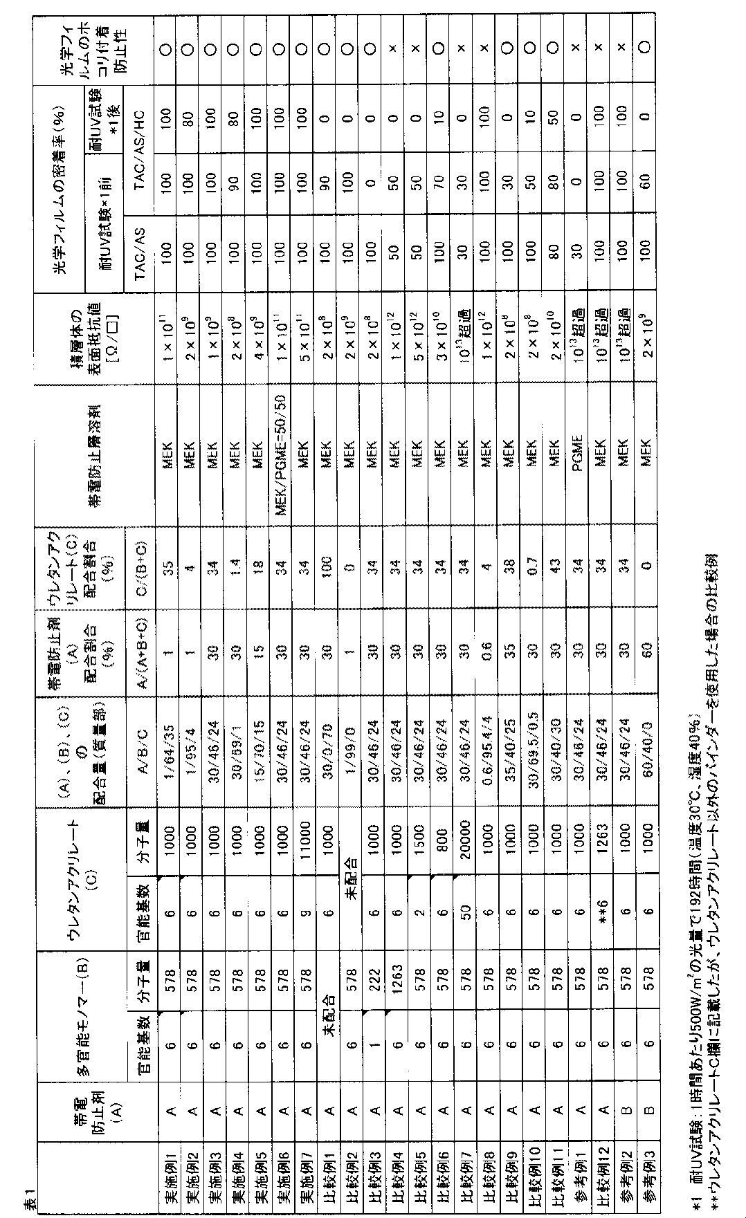
表1より、実施例1~7では、いずれも良好な積層体(帯電防止層)の表面抵抗値が得られ、光学フィルムの密着性も良好であった。また、光学特性や外観も良好であった。
10 トリアセチルセルロース基材
20 帯電防止層
30 ハードコート層
40 低屈折率層
50 保護フィルム
60 偏光層
70 偏光子
80 偏光板
Claims (11)
- (A)帯電防止剤、
(B)1分子中に光硬化性基を2個以上有し、分子量900以下の多官能モノマー及び
(C)1分子中にアクリロイル基及び/又はメタクリロイル基を6個以上有し、重量平均分子量1000~11000のウレタンアクリレートを含み、
当該(A)、(B)及び(C)の総量に対する当該(A)の割合が、1~30質量%、かつ、
当該(B)及び(C)の総量に対する当該(C)の割合が1~40質量%であることを特徴とする、帯電防止層用硬化性樹脂組成物。 - 前記(A)が、重量平均分子量1000~50000の4級アンモニウム塩であることを特徴とする、請求項1に記載の帯電防止層用硬化性樹脂組成物。
- さらに、(D)浸透性溶剤及び(E)非浸透性溶剤を含むことを特徴とする、請求項1又は2に記載の帯電防止層用硬化性樹脂組成物。
- 前記帯電防止層用硬化性樹脂組成物の膜厚1~5μmの硬化物の表面抵抗値が、1×10¹²Ω/□未満であることを特徴とする、請求項1乃至3のいずれか一項に記載の帯電防止層用硬化性樹脂組成物。
- トリアセチルセルロース基材の一面側に、当該トリアセチルセルロース基材側から膜厚1~5μmの帯電防止層、及びハードコート層が隣接して設けられている光学フィルムであって、
当該帯電防止層が前記請求項1乃至4のいずれか一項に記載の帯電防止層用硬化性樹脂組成物の硬化物からなり、
当該トリアセチルセルロース基材の帯電防止層側の界面近傍の領域には前記多官能モノマー(B)が浸透して硬化していることを特徴とする、光学フィルム。 - ホコリ付着防止性を有することを特徴とする、請求項5に記載の光学フィルム。
- 前記ハードコート層、当該帯電防止層及び前記トリアセチルセルロース基材間の碁盤目密着性試験の密着率が、90~100%であり、かつ、温度30℃、湿度40%において、紫外線を1時間当たり500W/m2の光量で192時間照射した後の当該密着率が、80~100%であることを特徴とする、請求項5又は6に記載の光学フィルム。
- 前記ハードコート層の帯電防止層とは反対側の面にさらに、低屈折率層が設けられていることを特徴とする、請求項5乃至7に記載の光学フィルム。
- 前記ハードコート層が、電離放射線硬化性樹脂を含む組成物の硬化物であることを特徴とする、請求項5乃至8のいずれかに記載の光学フィルム。
- 前記請求項5乃至9のいずれか一項に記載の光学フィルムのトリアセチルセルロース基材側に偏光子が設けられていることを特徴とする、偏光板。
- 前記請求項5乃至9のいずれか一項に記載の光学フィルムのトリアセチルセルロース基材側にディスプレイが配置されていることを特徴とする、ディスプレイパネル。
Priority Applications (3)
| Application Number | Priority Date | Filing Date | Title |
|---|---|---|---|
| JP2012524557A JP5811090B2 (ja) | 2010-07-12 | 2011-07-12 | 帯電防止層用硬化性樹脂組成物、光学フィルム、偏光板及びディスプレイパネル |
| CN201180031473.2A CN102958963B (zh) | 2010-07-12 | 2011-07-12 | 抗静电层用固化性树脂组合物、光学薄膜、偏振片以及显示面板 |
| KR1020137000846A KR101466520B1 (ko) | 2010-07-12 | 2011-07-12 | 대전 방지층용 경화성 수지 조성물, 광학 필름, 편광판 및 디스플레이 패널 |
Applications Claiming Priority (2)
| Application Number | Priority Date | Filing Date | Title |
|---|---|---|---|
| JP2010157808 | 2010-07-12 | ||
| JP2010-157808 | 2010-07-12 |
Publications (1)
| Publication Number | Publication Date |
|---|---|
| WO2012008444A1 true WO2012008444A1 (ja) | 2012-01-19 |
Family
ID=45469442
Family Applications (1)
| Application Number | Title | Priority Date | Filing Date |
|---|---|---|---|
| PCT/JP2011/065876 Ceased WO2012008444A1 (ja) | 2010-07-12 | 2011-07-12 | 帯電防止層用硬化性樹脂組成物、光学フィルム、偏光板及びディスプレイパネル |
Country Status (5)
| Country | Link |
|---|---|
| JP (1) | JP5811090B2 (ja) |
| KR (1) | KR101466520B1 (ja) |
| CN (2) | CN102958963B (ja) |
| TW (1) | TWI482705B (ja) |
| WO (1) | WO2012008444A1 (ja) |
Cited By (3)
| Publication number | Priority date | Publication date | Assignee | Title |
|---|---|---|---|---|
| CN107791632A (zh) * | 2017-11-24 | 2018-03-13 | 惠州市摩码菱丽光电材料有限公司 | 一种tac基材的低反射率无彩虹纹硬化保护膜及其制备方法 |
| CN116640524A (zh) * | 2023-05-10 | 2023-08-25 | 太湖金张科技股份有限公司 | 一种模切不掉粉的pu胶保护膜 |
| WO2024101232A1 (ja) * | 2022-11-07 | 2024-05-16 | Agc株式会社 | フィルム及び半導体パッケージの製造方法 |
Families Citing this family (5)
| Publication number | Priority date | Publication date | Assignee | Title |
|---|---|---|---|---|
| JP6235287B2 (ja) * | 2013-09-30 | 2017-11-22 | 日東電工株式会社 | 光学積層体 |
| WO2019124049A1 (ja) * | 2017-12-18 | 2019-06-27 | Dic株式会社 | 活性エネルギー線硬化性組成物、及び、それを用いたフィルム |
| CN108802885A (zh) * | 2018-04-23 | 2018-11-13 | 深圳市运宝莱光电科技有限公司 | 一种电磁屏蔽偏光片及制备方法 |
| JP7257165B2 (ja) * | 2019-02-12 | 2023-04-13 | 日東電工株式会社 | 補強フィルムを備えるデバイスおよびその製造方法、ならびに補強方法 |
| CN117087268B (zh) * | 2023-08-21 | 2025-09-19 | 湖南拓步电子科技有限公司 | 一种增强型抗静电触摸屏玻璃面板 |
Citations (3)
| Publication number | Priority date | Publication date | Assignee | Title |
|---|---|---|---|---|
| JP2006306008A (ja) * | 2005-03-31 | 2006-11-09 | Jsr Corp | 帯電防止用積層体 |
| JP2007332181A (ja) * | 2006-06-12 | 2007-12-27 | Nippon Kasei Chem Co Ltd | 帯電防止組成物、帯電防止層および帯電防止フィルム |
| JP2009086660A (ja) * | 2007-09-12 | 2009-04-23 | Dainippon Printing Co Ltd | 光学積層体、その製造方法、偏光板及び画像表示装置 |
Family Cites Families (2)
| Publication number | Priority date | Publication date | Assignee | Title |
|---|---|---|---|---|
| TWI416158B (zh) * | 2006-03-31 | 2013-11-21 | Dainippon Printing Co Ltd | Optical laminated body and optical laminate |
| KR101574351B1 (ko) * | 2008-09-16 | 2015-12-03 | 닛본 페인트 홀딩스 가부시키가이샤 | 내지문성 광경화성 조성물 및 내지문성 코팅층이 설치된 도장물 |
-
2011
- 2011-07-12 CN CN201180031473.2A patent/CN102958963B/zh active Active
- 2011-07-12 CN CN201410753543.0A patent/CN104530331B/zh active Active
- 2011-07-12 KR KR1020137000846A patent/KR101466520B1/ko active Active
- 2011-07-12 TW TW100124540A patent/TWI482705B/zh active
- 2011-07-12 JP JP2012524557A patent/JP5811090B2/ja active Active
- 2011-07-12 WO PCT/JP2011/065876 patent/WO2012008444A1/ja not_active Ceased
Patent Citations (3)
| Publication number | Priority date | Publication date | Assignee | Title |
|---|---|---|---|---|
| JP2006306008A (ja) * | 2005-03-31 | 2006-11-09 | Jsr Corp | 帯電防止用積層体 |
| JP2007332181A (ja) * | 2006-06-12 | 2007-12-27 | Nippon Kasei Chem Co Ltd | 帯電防止組成物、帯電防止層および帯電防止フィルム |
| JP2009086660A (ja) * | 2007-09-12 | 2009-04-23 | Dainippon Printing Co Ltd | 光学積層体、その製造方法、偏光板及び画像表示装置 |
Cited By (3)
| Publication number | Priority date | Publication date | Assignee | Title |
|---|---|---|---|---|
| CN107791632A (zh) * | 2017-11-24 | 2018-03-13 | 惠州市摩码菱丽光电材料有限公司 | 一种tac基材的低反射率无彩虹纹硬化保护膜及其制备方法 |
| WO2024101232A1 (ja) * | 2022-11-07 | 2024-05-16 | Agc株式会社 | フィルム及び半導体パッケージの製造方法 |
| CN116640524A (zh) * | 2023-05-10 | 2023-08-25 | 太湖金张科技股份有限公司 | 一种模切不掉粉的pu胶保护膜 |
Also Published As
| Publication number | Publication date |
|---|---|
| CN104530331A (zh) | 2015-04-22 |
| KR20130054314A (ko) | 2013-05-24 |
| CN102958963B (zh) | 2014-11-05 |
| JPWO2012008444A1 (ja) | 2013-09-09 |
| JP5811090B2 (ja) | 2015-11-11 |
| TWI482705B (zh) | 2015-05-01 |
| CN104530331B (zh) | 2017-01-11 |
| CN102958963A (zh) | 2013-03-06 |
| TW201223758A (en) | 2012-06-16 |
| KR101466520B1 (ko) | 2014-11-27 |
Similar Documents
| Publication | Publication Date | Title |
|---|---|---|
| JP5779863B2 (ja) | 光学フィルムの製造方法、光学フィルム、偏光板及びディスプレイ | |
| JP5381570B2 (ja) | ハードコートフィルムの製造方法、ハードコートフィルム、偏光板及びディスプレイパネル | |
| JP5811090B2 (ja) | 帯電防止層用硬化性樹脂組成物、光学フィルム、偏光板及びディスプレイパネル | |
| JP5846121B2 (ja) | ハードコート層用硬化性樹脂組成物、ハードコートフィルムの製造方法、ハードコートフィルム、偏光板及びディスプレイパネル | |
| TWI522642B (zh) | 光學薄膜、偏光板、顯示面板及顯示器 | |
| JP5262032B2 (ja) | 光学積層体の製造方法、光学積層体、偏光板及び画像表示装置 | |
| JP5984198B2 (ja) | ハードコートフィルム、偏光板、画像表示装置、ハードコート層の密着性向上方法およびハードコートフィルムの製造方法 | |
| US7709084B2 (en) | Anti-newton ring sheet and touch panel using the same | |
| KR102066759B1 (ko) | 하드 코팅 조성물 및 고굴절률 안티블로킹층 형성 조성물 | |
| JP2008012675A (ja) | 光学積層体、及びその製造方法 | |
| KR101809757B1 (ko) | 하드 코트 필름, 하드 코트 필름의 제조 방법, 편광판, 전방면판 및 화상 표시 장치 | |
| JP5753285B2 (ja) | 光学積層体 | |
| JP2013142793A (ja) | ハードコートフィルム及びその製造方法、反射防止フィルム | |
| JP5750848B2 (ja) | 画像表示装置用光学部材 | |
| JP2004126220A (ja) | 反射防止透明基板および画像表示装置 | |
| JP2008087279A (ja) | ハードコートフィルム又はシート | |
| JP2001247792A (ja) | 放射線硬化型樹脂組成物の硬化皮膜を有するフィルム | |
| JP2003313260A (ja) | 放射線硬化型樹脂組成物及びその硬化皮膜を有するフィルム |
Legal Events
| Date | Code | Title | Description |
|---|---|---|---|
| WWE | Wipo information: entry into national phase |
Ref document number: 201180031473.2 Country of ref document: CN |
|
| 121 | Ep: the epo has been informed by wipo that ep was designated in this application |
Ref document number: 11806774 Country of ref document: EP Kind code of ref document: A1 |
|
| WWE | Wipo information: entry into national phase |
Ref document number: 2012524557 Country of ref document: JP |
|
| ENP | Entry into the national phase |
Ref document number: 20137000846 Country of ref document: KR Kind code of ref document: A |
|
| NENP | Non-entry into the national phase |
Ref country code: DE |
|
| 122 | Ep: pct application non-entry in european phase |
Ref document number: 11806774 Country of ref document: EP Kind code of ref document: A1 |